Datasheet CD74ACT541SM, CD74ACT541M96, CD74ACT541M, CD74ACT541E, CD74ACT540M96 Datasheet (Texas Instruments)
...Page 1
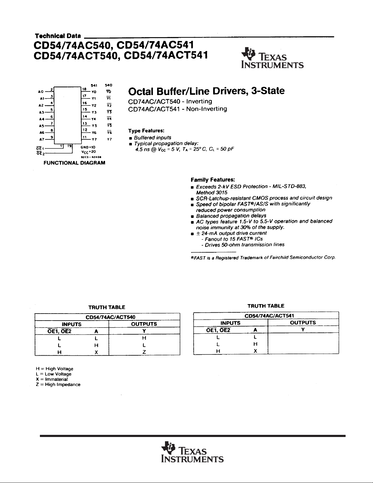
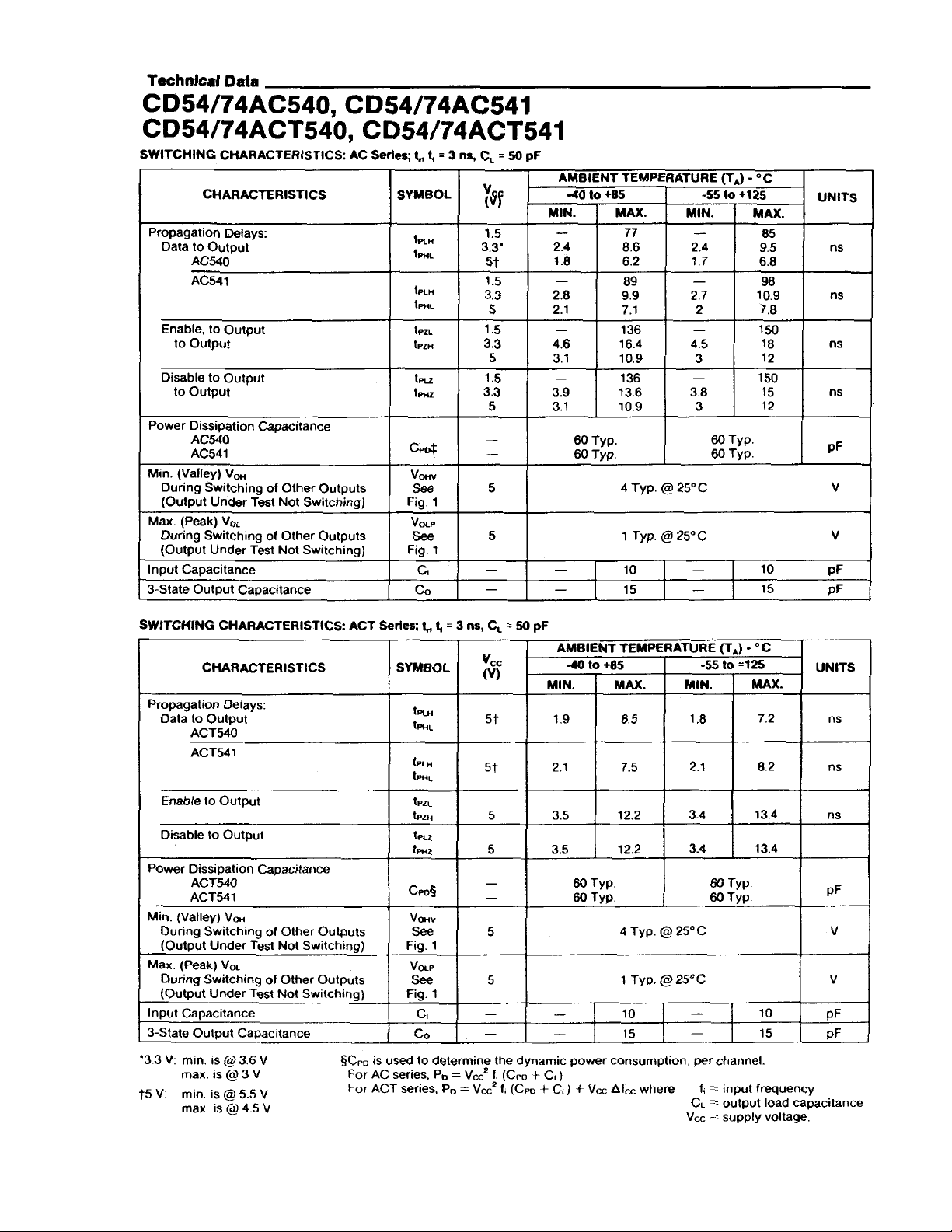
The CD54/74AC540, -541, and CD54/74ACT540, -541 octal
buffer/line drivers use the RCA ADV ANCED CMOS technology . The
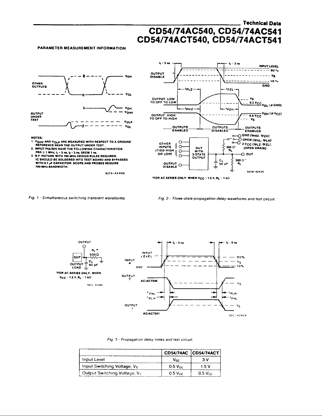
CD54/74AC/ACT540 are inverting 3-state buffers having two
active-LOW output enables. The CD54/74AC/ACT541 are
non-inverting 3-state buffers having two active-LOW output enables.
The CD74AC540, -541, and CD74ACT540, -541 are supplied in
20-lead dual-in-line plastic packages (E suffix) and in 20-lead
dual-in-line small-outline plastic packages (M suffix). Both package
types are operable over the following temperature ranges: Industrial
(–40 to +85°C) and Extended Industrial/Military (–55 to +125°C).
Data sheet acquired from Harris Semiconductor
SCHS285A – Revised November 1999
The CD54AC540, -541, and CD54ACT540, -541, available in chip
form (H suffix), are operable over the –55 to +125°C temperature
range.
L
H
Z
PRODUCTION DATA information is current as of publication date.
Products conform to specifications per the terms of Texas Instruments
standard warranty. Production processing does not necessarily include
testing of all parameters.
POST OFFICE BOX 655303 • DALLAS, TEXAS 75265
Copyright 1999, Texas Instruments Incorporated
1
Page 2
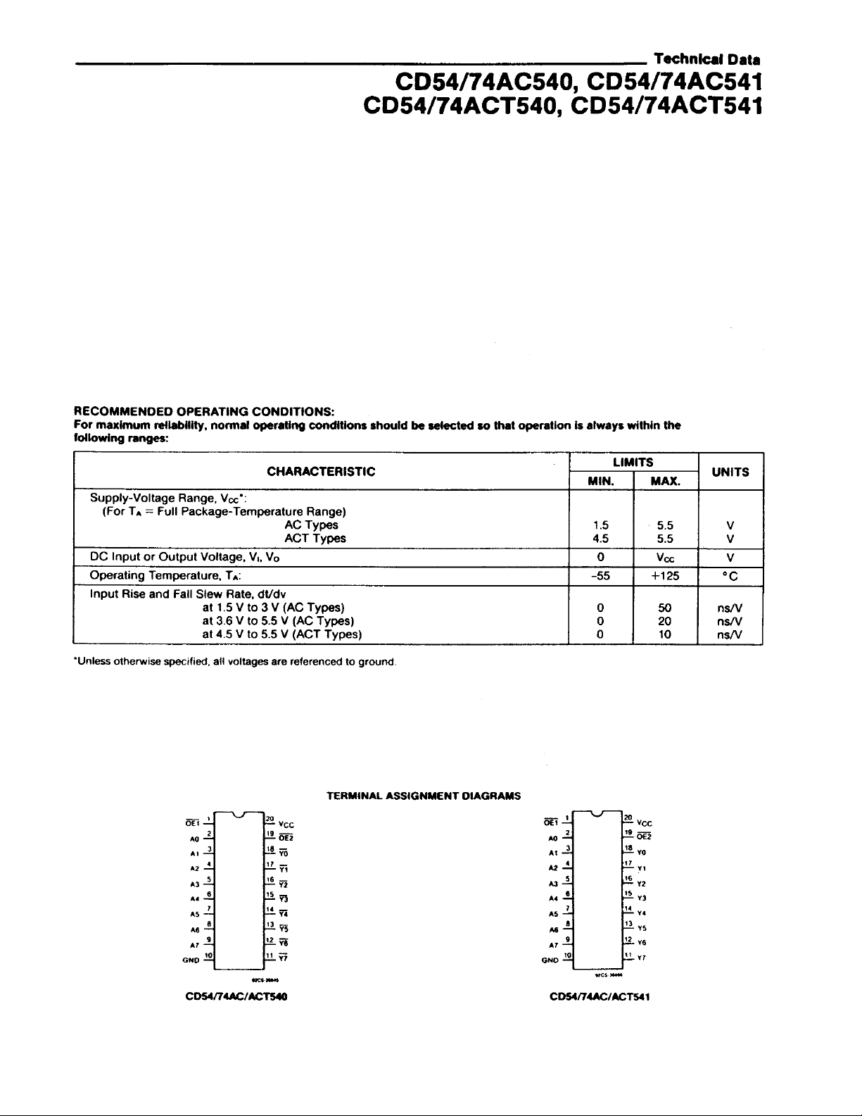
MAXIMUM RATINGS,
DC SUPPLY-VOLTAGE (VCC) –0.5 to 6 V. . . . . . . . . . . . . . . . . . . . . . . . . . . . . . . . . . . . . . . . . . . . . . . . . . . . . . . . . . . . . . . . . . . . . . . . . . . . . . . . . .
DC INPUT DIODE CURRENT, IIK (for VI < –0.5 or VI > VCC + 0.5 V) ±20 mA. . . . . . . . . . . . . . . . . . . . . . . . . . . . . . . . . . . . . . . . . . . . . . . . . . .
DC OUTPUT DIODE CURRENT, IOK (for VO < –0.5 or VO > VCC + 0.5 V) ±50 mA. . . . . . . . . . . . . . . . . . . . . . . . . . . . . . . . . . . . . . . . . . . . . .
DC OUTPUT SOURCE OR SINK CURRENT per Output Pin, IO (for VO > –0.5 or VO < VCC + 0.5 V) ±50 mA. . . . . . . . . . . . . . . . . . . . . . .
DC VCC OR GROUND CURRENT (ICC or I
PACKAGE THERMAL IMPEDANCE, θJA (see Note 1): E package 69°C/W. . . . . . . . . . . . . . . . . . . . . . . . . . . . . . . . . . . . . . . . . . . . . . . . . . . . . .
STORAGE TEMPERATURE (T
LEAD TEMPERATURE (DURING SOLDERING):
At distance 1/16 ± 1/32 in. (1.59 ± 0.79 mm) from case for 10 s maximum +265°C. . . . . . . . . . . . . . . . . . . . . . . . . . . . . . . . . . . . . . . . . . . . .
Unit inserted into PC board min. thickness 1/16 in. (1.59 mm) with solder contacting lead tips only +300°C. . . . . . . . . . . . . . . . . . . . . . . .
* For up to 4 outputs per device: add ±25 mA for each additional output.
NOTE 1: The package thermal impedance is calculated in accordance with JESD 51.
Absolute-Maximum Values:
GND
) –65 to +150°C. . . . . . . . . . . . . . . . . . . . . . . . . . . . . . . . . . . . . . . . . . . . . . . . . . . . . . . . . . . . . . . . . . . . . . . . . . .
stg
) ±100 mA*. . . . . . . . . . . . . . . . . . . . . . . . . . . . . . . . . . . . . . . . . . . . . . . . . . . . . . . . . . . . . . . . . .
M package 58°C/W. . . . . . . . . . . . . . . . . . . . . . . . . . . . . . . . . . . . . . . . . . . . . . . . . . . . .
2
POST OFFICE BOX 655303 • DALLAS, TEXAS 75265
Page 3
POST OFFICE BOX 655303 • DALLAS, TEXAS 75265
3
Page 4
4
POST OFFICE BOX 655303 • DALLAS, TEXAS 75265
Page 5
POST OFFICE BOX 655303 • DALLAS, TEXAS 75265
ns
5
Page 6
6
POST OFFICE BOX 655303 • DALLAS, TEXAS 75265
Page 7

IMPORTANT NOTICE
T exas Instruments and its subsidiaries (TI) reserve the right to make changes to their products or to discontinue
any product or service without notice, and advise customers to obtain the latest version of relevant information
to verify, before placing orders, that information being relied on is current and complete. All products are sold
subject to the terms and conditions of sale supplied at the time of order acknowledgement, including those
pertaining to warranty, patent infringement, and limitation of liability.
TI warrants performance of its semiconductor products to the specifications applicable at the time of sale in
accordance with TI’s standard warranty. Testing and other quality control techniques are utilized to the extent
TI deems necessary to support this warranty . Specific testing of all parameters of each device is not necessarily
performed, except those mandated by government requirements.
CERTAIN APPLICATIONS USING SEMICONDUCTOR PRODUCTS MAY INVOLVE POTENTIAL RISKS OF
DEATH, PERSONAL INJURY, OR SEVERE PROPERTY OR ENVIRONMENTAL DAMAGE (“CRITICAL
APPLICATIONS”). TI SEMICONDUCTOR PRODUCTS ARE NOT DESIGNED, AUTHORIZED, OR
WARRANTED TO BE SUITABLE FOR USE IN LIFE-SUPPORT DEVICES OR SYSTEMS OR OTHER
CRITICAL APPLICA TIONS. INCLUSION OF TI PRODUCTS IN SUCH APPLICATIONS IS UNDERST OOD TO
BE FULLY AT THE CUSTOMER’S RISK.
In order to minimize risks associated with the customer’s applications, adequate design and operating
safeguards must be provided by the customer to minimize inherent or procedural hazards.
TI assumes no liability for applications assistance or customer product design. TI does not warrant or represent
that any license, either express or implied, is granted under any patent right, copyright, mask work right, or other
intellectual property right of TI covering or relating to any combination, machine, or process in which such
semiconductor products or services might be or are used. TI’s publication of information regarding any third
party’s products or services does not constitute TI’s approval, warranty or endorsement thereof.
Copyright 1999, Texas Instruments Incorporated
 Loading...