

查询CD74AC138供应商
Data sheet acquired from Harris Semiconductor
SCHS234
CD74A C138, CD74ACT138,
CD74A C238, CD74ACT238
[ /Title
(CD74
AC138
,
CD74
ACT13
8,
CD74
AC238
,
CD74
ACT23
8)
/Subject (3to-8Line
Decoders/De
multiplexers)
/Autho
r ()
/Keywords
(Harris
Semiconductor,
Advan
ced
September 1998
Features
• CD74AC138, CD74ACT138 . . . . . . . . . . . . . . . Inverting
• CD74AC238, CD74ACT238 . . . . . . . . . . . Non-Inverting
• Buffered Inputs
• Typical Propagation Delay
- 5ns at V
• Exceeds 2kV ESD Protection MIL-STD-883, Method
3015
• SCR-Latchup-Resistant CMOS Process and Circuit
Design
• Speed of Bipolar FAST™/AS/S with Significantly
Reduced Power Consumption
• Balanced Propagation Delays
• AC Types Feature 1.5V to 5.5V Operation and
Balanced Noise Immunity at 30% of the Supply
• ±24mA Output Drive Current
- Fanout to 15 FAST™ ICs
- Drives 50Ω Transmission Lines
= 5V, TA = 25oC, CL = 50pF
CC
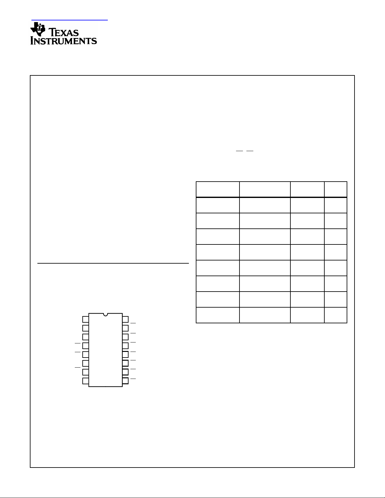
Pinout
CD74AC138, CD74ACT138, CD74AC238, CD74ACT238
(PDIP, SOIC)
TOP VIEW
V
A0
A1
A2
E1
E2
E3
AC/ACT138
AC/ACT238 Y7
Y7
GND
1
2
3
4
5
6
7
8
16
CC
Y0 AC/ACT138
15
Y0 AC/ACT238
Y1 AC/ACT138
14
Y1 AC/ACT238
Y2 AC/ACT138
13
Y2 AC/ACT238
Y3 AC/ACT138
12
Y3 AC/ACT238
Y4 AC/ACT138
11
Y4 AC/ACT238
Y5 AC/ACT138
10
Y5 AC/ACT238
9
Y6 AC/ACT138
Y6 AC/ACT238
3-to-8-Line Decoders/Demultiplexers
Description
The CD74AC138, CD74ACT138, CD74AC238, and
CD74ACT238 are 3-to-8-line decoders/demultiplexers that
utilize the Harris Advanced CMOS Logic technology. Both
circuits have three binary select inputs (A0, A1, and A2). If
the device is enabled, these inputs determine which one of
the eight normally HIGH outputs of the AC/ACT138 will go
LOW or which on of the normally LOW outputs of the
AC/ACT238 will go HIGH. Two active LOW and one active
HIGH enables (
cascading of these devices.
Ordering Information
PART
NUMBER
CD74AC138E 0 to 70oC, -40 to 85,
CD74ACT138E 0 to 70oC, -40 to 85,
CD74AC238E 0 to 70oC, -40 to 85,
CD74ACT238E 0 to 70oC, -40 to 85,
CD74AC138M 0 to 70oC, -40 to 85,
CD74ACT138M 0 to 70oC, -40 to 85,
CD74AC238M 0 to 70oC, -40 to 85,
CD74ACT238M 0 to 70oC, -40 to 85,
NOTES:
17. When ordering, use the entire part number. Add the suffix 96 to
obtain the variant in the tape and reel.
18. Waferanddieforthis part number is availablewhich meets all electrical specifications. Please contact your local sales office or Harris
customer service for ordering information.
E1, E2 and E3) are provided to simplify the
TEMP.
RANGE (oC) PACKAGE
16 Ld PDIP E16.3
-55 to 125
16 Ld PDIP E16.3
-55 to 125
16 Ld PDIP E16.3
-55 to 125
16 Ld PDIP E16.3
-55 to 125
16 Ld SOIC M16.15
-55 to 125
16 Ld SOIC M16.15
-55 to 125
16 Ld SOIC M16.15
-55 to 125
16 Ld SOIC M16.15
-55 to 125
PKG.
NO.
CAUTION: These devices are sensitive to electrostatic discharge. Users should follow proper IC Handling Procedures.
FAST™ is a Trademark of Fairchild Semiconductor.
Copyright
© Harris Corporation 1998
1
File Number 1909.1
CD74AC138, CD74ACT138, CD74AC238, CD74ACT238
Functional Diagram
AC/ACT
AC/ACT
238
Y1
Y2
Y3
Y4
Y5
Y6
Y7
138
Y0
Y1
Y2
Y3
Y4
Y5
Y6
Y7
OUTPUTSENABLE ADDRESS
1
A0 Y0
2
A1
3
A2
4
E1
5
E2
6
E3
15
14
13
12
11
10
9
7
CD74AC/ACT138 TRUTH TABLE
INPUTS
(NOTE 4)
E
3
E0 A
2
A
1
A
0
Y0 Y1 Y2 Y3 Y4 Y5 Y6 Y7
XH XXXHHHHHHHH
LX XXXHHHHHHHH
HL LL LLHHHHHHH
HL LLHHLHHHHHH
HL LHLHHLHHHHH
HL LHHHHHLHHHH
HL HLLHHHHLHHH
HL HLLHHHHHLHH
HL HHLHHHHHHLH
HL HHHHHHHHHHL
CD74AC/ACT238 TRUTH TABLE
INPUTS
OUTPUTSENABLE ADDRESS
(NOTE 4)
E
3
E0 A
2
A
1
A
0
Y0 Y1 Y2 Y3 Y4 Y5 Y6 Y7
XHXXXLLLLLLLL
LX XXXLLLLLLLL
HL LLLHLLLLLLL
HL LLHLHLLLLLL
HL LHLLLHLLLLL
HL LHHLLLHLLLL
HL HLLLLLLHLLL
HL HLHLLLLLHLL
HL HHLLLLLLLHL
HL HHHLLLLLLLH
NOTES:
19. H = High Level, L = Low Level, X = Don’t Care
20.
E0 = E1 + E2
2
CD74AC138, CD74ACT138, CD74AC238, CD74ACT238
Absolute Maximum Ratings Thermal Information
DC Supply Voltage, VCC. . . . . . . . . . . . . . . . . . . . . . . . -0.5V to 6V
DC Input Diode Current, I
IK
For VI < -0.5V or VI > VCC + 0.5V. . . . . . . . . . . . . . . . . . . . . .±20mA
DC Output Diode Current, I
OK
For VO < -0.5V or VO > VCC + 0.5V . . . . . . . . . . . . . . . . . . . .±50mA
DC Output Source or Sink Current per Output Pin, I
O
For VO > -0.5V or VO < VCC + 0.5V . . . . . . . . . . . . . . . . . . . .±50mA
DC VCC or Ground Current, I
CC orIGND
(Note 5) . . . . . . . . .±100mA
Operating Conditions
Temperature Range, TA . . . . . . . . . . . . . . . . . . . . . . -55oC to 125oC
Supply Voltage Range, VCC (Note 6)
AC Types. . . . . . . . . . . . . . . . . . . . . . . . . . . . . . . . . . .1.5V to 5.5V
ACT Types . . . . . . . . . . . . . . . . . . . . . . . . . . . . . . . . .4.5V to 5.5V
DC Input or Output Voltage, VI, VO . . . . . . . . . . . . . . . . . 0V to V
Input Rise and Fall Slew Rate, dt/dv
AC Types, 1.5V to 3V . . . . . . . . . . . . . . . . . . . . . . . . . 50ns (Max)
AC Types, 3.6V to 5.5V. . . . . . . . . . . . . . . . . . . . . . . . 20ns (Max)
ACT Types, 4.5V to 5.5V. . . . . . . . . . . . . . . . . . . . . . . 10ns (Max)
CAUTION: Stresses above those listed in “Absolute Maximum Ratings” may cause permanent damage to the device. This is a stress only rating and operation
of the device at these or any other conditions above those indicated in the operational sections of this specification is not implied.
NOTES:
21. For up to 4 outputs per device, add ±25mA for each additional output.
22. Unless otherwise specified, all voltages are referenced to ground.
23. θJA is measured with the component mounted on an evaluation PC board in free air.
Thermal Resistance (Typical, Note 7) θJA (oC/W)
PDIP Package. . . . . . . . . . . . . . . . . . . . . . . . . . . . . 90
SOIC Package. . . . . . . . . . . . . . . . . . . . . . . . . . . . . 160
Maximum Junction Temperature (Plastic Package) . . . . . . . . . . 150oC
Maximum Storage Temperature Range . . . . . . . . . .-65oC to 150oC
Maximum Lead Temperature (Soldering 10s) . . . . . . . . . . . . .300oC
CC
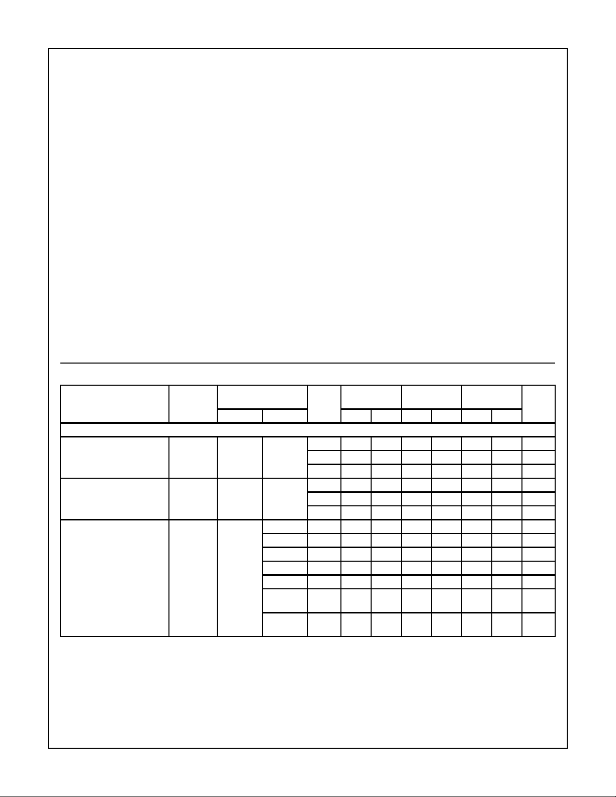
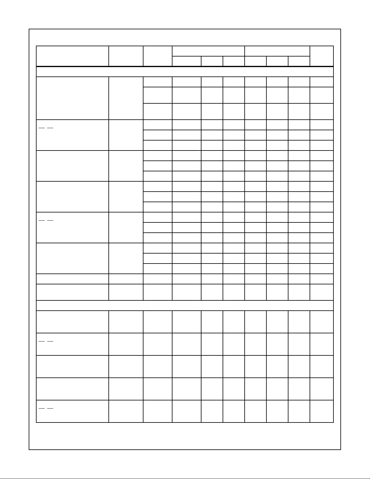
DC Electrical Specifications
PARAMETER SYMBOL
AC TYPES
High Level Input Voltage V
Low Level Input Voltage V
High Level Output Voltage V
IH
IL
OH
TEST
CONDITIONS
(V) IO(mA) MIN MAX MIN MAX MIN MAX
I
V
CC
(V)
25
o
C
-40oC TO
85oC
-55oC TO
125oC
- - 1.5 1.2 - 1.2 - 1.2 - V
3 2.1 - 2.1 - 2.1 - V
5.5 3.85 - 3.85 - 3.85 - V
- - 1.5 - 0.3 - 0.3 - 0.3 V
3 - 0.9 - 0.9 - 0.9 V
5.5 - 1.65 - 1.65 - 1.65 V
VIH or V
-0.05 1.5 1.4 - 1.4 - 1.4 - V
IL
-0.05 3 2.9 - 2.9 - 2.9 - V
-0.05 4.5 4.4 - 4.4 - 4.4 - V
-4 3 2.58 - 2.48 - 2.4 - V
-24 4.5 3.94 - 3.8 - 3.7 - V
-75
5.5 - - 3.85 - - - V
(Note 8, 9)
-50
5.5----3.85 - V
(Note 8, 9)
UNITSV
3
CD74AC138, CD74ACT138, CD74AC238, CD74ACT238
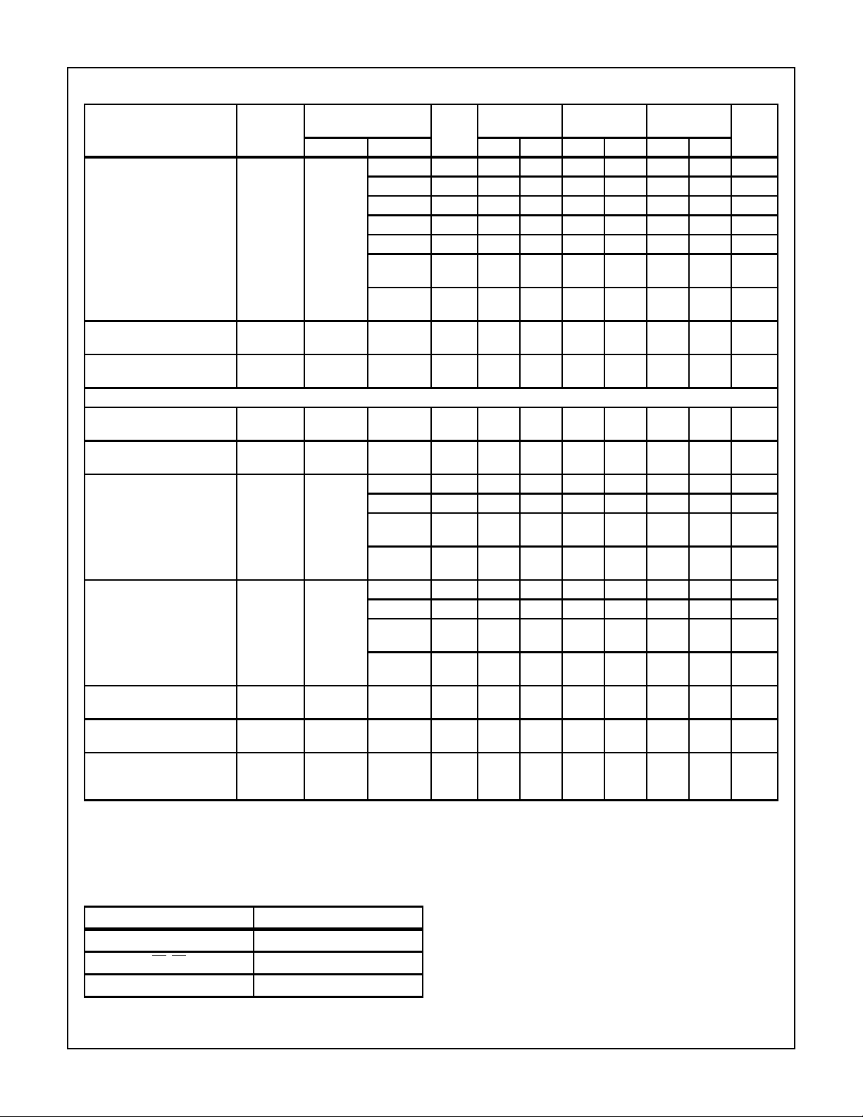
DC Electrical Specifications (Continued)
PARAMETER SYMBOL
Low Level Output Voltage V
OL
TEST
CONDITIONS
(V) IO(mA) MIN MAX MIN MAX MIN MAX
I
VIH or V
0.05 1.5 - 0.1 - 0.1 - 0.1 V
IL
V
CC
(V)
25
o
C
0.05 3 - 0.1 - 0.1 - 0.1 V
0.05 4.5 - 0.1 - 0.1 - 0.1 V
12 3 - 0.36 - 0.44 - 0.5 V
24 4.5 - 0.36 - 0.44 - 0.5 V
75
5.5 - - - 1.65 - - V
(Note 8, 9)
50
5.5-----1.65 V
(Note 8, 9)
Input Leakage Current I
I
VCC or
- 5.5 - ±0.1 - ±1-±1µA
GND
Quiescent Supply Current
MSI
I
CC
VCC or
GND
0 5.5 - 8 - 80 - 160 µA
ACT TYPES
High Level Input Voltage V
IH
- - 4.5 to
2-2-2-V
5.5
Low Level Input Voltage V
IL
- - 4.5 to
- 0.8 - 0.8 - 0.8 V
5.5
High Level Output Voltage V
OH
VIH or V
-0.05 4.5 4.4 - 4.4 - 4.4 - V
IL
-24 4.5 3.94 - 3.8 - 3.7 - V
-75
5.5 - - 3.85 - - - V
(Note 8, 9)
-50
5.5----3.85 - V
(Note 8, 9)
Low Level Output Voltage V
OL
VIH or V
0.05 4.5 - 0.1 - 0.1 - 0.1 V
IL
24 4.5 - 0.36 - 0.44 - 0.5 V
75
5.5 - - - 1.65 - - V
(Note 8, 9)
50
5.5-----1.65 V
(Note 8, 9)
Input Leakage Current I
I
VCC or
- 5.5 - ±0.1 - ±1-±1µA
GND
Quiescent Supply Current
MSI
AdditionalSupplyCurrent per
Input Pin TTL Inputs High
I
CC
VCC or
GND
∆I
CC
V
CC
-2.1
0 5.5 - 8 - 80 - 160 µA
- 4.5 to
- 2.4 - 2.8 - 3 mA
5.5
1 Unit Load
NOTES:
24. Test one output at a time for a 1-second maximum duration. Measurement is made by forcing current and measuring voltage to minimize
power dissipation.
o
25. Test verifies a minimum 50Ω transmission-line-drive capability at 85
C, 75Ω at 125oC.
-40oC TO
85oC
-55oC TO
125oC
UNITSV
ACT Input Load Table
INPUT UNIT LOAD
A0-A2 0.83
E1, E2 1
E3 0.42
NOTE: Unit load is ∆ICClimit specified in DC Electrical Specifications
Table, e.g., 2.4mA max at 25oC.
4
CD74AC138, CD74ACT138, CD74AC238, CD74ACT238
Switching Specifications Input t
PARAMETER SYMBOL V
AC TYPES
Propagation Delay,
An to Output
(CD74AC/ACT138)
Propagation Delay,
E1, E2 to Output
(CD74AC/ACT138)
Propagation Delay,
E3 to Output
(CD74AC/ACT138)
Propagation Delay,
An to Output
(CD74AC/ACT238)
Propagation Delay,
E1, E2 to Output
(CD74AC/ACT238)
Propagation Delay,
E3 to Output
(CD74AC/ACT238)
Input Capacitance C
Power Dissipation Capacitance C
ACT TYPES
Propagation Delay,
An to Output
(CD74AC/ACT138)
Propagation Delay,
E1, E2 to Output
(CD74AC/ACT138)
Propagation Delay,
E3 to Output
(CD74AC/ACT138)
Propagation Delay,
An to Output
(CD74AC/ACT238)
Propagation Delay,
E1, E2 to Output
(CD74AC/ACT238)
t
PLH
t
PLH
t
PLH
t
PLH
t
PLH
t
PLH
(Note 13)
t
PLH
t
PLH
t
PLH
t
PLH
t
PLH
, tf = 3ns, CL= 50pF (Worst Case)
r
(V)
CC
, t
PHL
1.5 - - 125 - - 138 ns
3.3
4 - 14 3.9 - 15.4 ns
(Note 11)
5
2.8 - 10 2.8 - 11 ns
(Note 12)
, t
PHL
1.5 - - 114 - - 125 ns
3.3 3.6 - 12.7 3.5 - 14 ns
5 2.6 - 9.1 2.5 - 10 ns
, t
PHL
1.5 - - 125 - - 138 ns
3.3 4 - 14 3.9 - 15.4 ns
5 2.8 - 10 2.8 - 11 ns
, t
PHL
1.5 - - 170 - - 187 ns
3.3 5.4 - 19.1 5.3 - 21 ns
5 3.9 - 13.6 3.8 - 15 ns
, t
PHL
1.5 - - 135 - - 149 ns
3.3 4.3 - 15.2 4.2 - 16.7 ns
5 3.1 - 10.7 3 - 11.9 ns
, t
PHL
1.5 - - 189 - - 208 ns
3.3 6 - 21.1 5.8 - 23.2 ns
5 4.3 - 15.1 4.2 - 16.6 ns
- - -10- -10pF
- - 110 - - 110 - pF
5
3.1 - 10.9 3 - 12 ns
PD
, t
I
PHL
(Note 12)
, t
PHL
, t
PHL
, t
PHL
, t
PHL
5 2.7 - 9.5 2.6 - 10.5 ns
5 2.8 - 10 2.8 - 11 ns
5 4 - 14.2 3.9 - 15.6 ns
5 3.7 - 12.9 3.6 - 14.2 ns
-40oC TO 85oC -55oC TO 125oC
UNITSMIN TYP MAX MIN TYP MAX
5

CD74AC138, CD74ACT138, CD74AC238, CD74ACT238
Switching Specifications Input t
, tf = 3ns, CL= 50pF (Worst Case) (Continued)
r
-40oC TO 85oC -55oC TO 125oC
PARAMETER SYMBOL V
Propagation Delay,
t
PLH
, t
PHL
(V)
CC
5 3.5 - 12.4 3.4 - 13.6 ns
E3 to Output
(CD74AC/ACT238)
Input Capacitance C
Power Dissipation Capacitance C
I
PD
- - -10- -10pF
- - 110 - - 110 - pF
(Note 13)
NOTES:
26. Limits tested at 100%.
27. 3.3V Min at 3.6V, Max at 3V.
28. 5V Min at 5.5V, Max at 4.5V.
29. CPD is used to determine the dynamic power consumption per package.
AC: PD = V
ACT: PD = V
tr = 3ns
INPUT
2
fi(CPD + CL)
CC
2
fi(CPD + CL) + VCC∆ICC where fi = input frequency, CL = output load capacitance, VCC = supply voltage.
CC
= 3ns
t
f
90%
V
S
10%
GND
E1, E2
E3
= 3ns
t
r
INPUT
= 3ns
t
f
UNITSMIN TYP MAX MIN TYP MAX
90%
V
S
GND
138 OUTPUT
238 OUTPUT
t
PLH
t
PHL
t
PLH
t
PHL
V
S
V
S
FIGURE 8. PROPAGATION DELAY TIMES FIGURE 9. PROPAGATION DELAY TIMES
OUTPUT
R
(NOTE)
L
C
L
50pF
500Ω
DUT
OUTPUT
LOAD
NOTE: For AC Series Only: When VCC = 1.5V, RL = 1kΩ.
CD74AC CD74ACT
Input Level V
Input Switching Voltage, V
Output Switching Voltage, V
S
S
0.5 V
0.5 V
CC
CC
CC
FIGURE 10. PROPAGATION DELAY TIMES
3V
1.5V
0.5 V
CC
138 OUTPUT
238 OUTPUT
t
t
PHL
PLH
t
PLH
t
PHL
V
S
V
S
6

IMPORTANT NOTICE
T exas Instruments and its subsidiaries (TI) reserve the right to make changes to their products or to discontinue
any product or service without notice, and advise customers to obtain the latest version of relevant information
to verify, before placing orders, that information being relied on is current and complete. All products are sold
subject to the terms and conditions of sale supplied at the time of order acknowledgement, including those
pertaining to warranty, patent infringement, and limitation of liability.
TI warrants performance of its semiconductor products to the specifications applicable at the time of sale in
accordance with TI’s standard warranty. Testing and other quality control techniques are utilized to the extent
TI deems necessary to support this warranty . Specific testing of all parameters of each device is not necessarily
performed, except those mandated by government requirements.
CERT AIN APPLICATIONS USING SEMICONDUCTOR PRODUCTS MAY INVOLVE POTENTIAL RISKS OF
DEATH, PERSONAL INJURY, OR SEVERE PROPERTY OR ENVIRONMENTAL DAMAGE (“CRITICAL
APPLICATIONS”). TI SEMICONDUCTOR PRODUCTS ARE NOT DESIGNED, AUTHORIZED, OR
WARRANTED TO BE SUITABLE FOR USE IN LIFE-SUPPORT DEVICES OR SYSTEMS OR OTHER
CRITICAL APPLICA TIONS. INCLUSION OF TI PRODUCTS IN SUCH APPLICATIONS IS UNDERST OOD TO
BE FULLY AT THE CUSTOMER’S RISK.
In order to minimize risks associated with the customer’s applications, adequate design and operating
safeguards must be provided by the customer to minimize inherent or procedural hazards.
TI assumes no liability for applications assistance or customer product design. TI does not warrant or represent
that any license, either express or implied, is granted under any patent right, copyright, mask work right, or other
intellectual property right of TI covering or relating to any combination, machine, or process in which such
semiconductor products or services might be or are used. TI’s publication of information regarding any third
party’s products or services does not constitute TI’s approval, warranty or endorsement thereof.
Copyright 1999, Texas Instruments Incorporated
 Loading...