

Texas Instruments CD74HCT4538M96, CD74HCT4538M, CD74HCT4538E, CD74HC4538PWR, CD74HC4538M96 Datasheet
...
Data sheet acquired from Harris Semiconductor
/
j
SCHS123
June 1998
CD54HC4538, CD74HC4538,
CD74HCT4538
High Speed CMOS Logic Dual Retriggerable
Precision Monostable Multivibrator
[ /Title
(CD54
HC453
8,
CD74
HC453
8,
CD74
HCT45
38)
Subect
(High
Speed
CMOS
Logic
Features
• Retriggerable/Resettable Capability
• Trigger and Reset Propagation Delays Independent of
R
, C
X
X
• Triggering from the Leading or Trailing Edge
• Q and
Q Buffered Outputs Available
• Separate Resets
• Wide Range of Output-Pulse Widths
• Schmitt Trigger Input on A and
• Retrigger Time is Independent of C
B Inputs
X
• Fanout (Over Temperature Range)
- Standard Outputs. . . . . . . . . . . . . . . 10 LSTTL Loads
- Bus Driver Outputs . . . . . . . . . . . . . 15 LSTTL Loads
• Wide Operating Temperature Range . . . -55
o
C to 125oC
• Balanced Propagation Delay and Transition Times
• Significant Power Reduction Compared to LSTTL
Logic ICs
• HC Types
- 2V to 6V Operation
- High Noise Immunity: N
= 30%, NIH = 30% of V
IL
CC
at VCC = 5V
• HCT Types
- 4.5V to 5.5V Operation
- Direct LSTTL Input Logic Compatibility,
V
= 0.8V (Max), VIH = 2V (Min)
IL
- CMOS Input Compatibility, I
≤ 1µA at VOL, V
l
OH
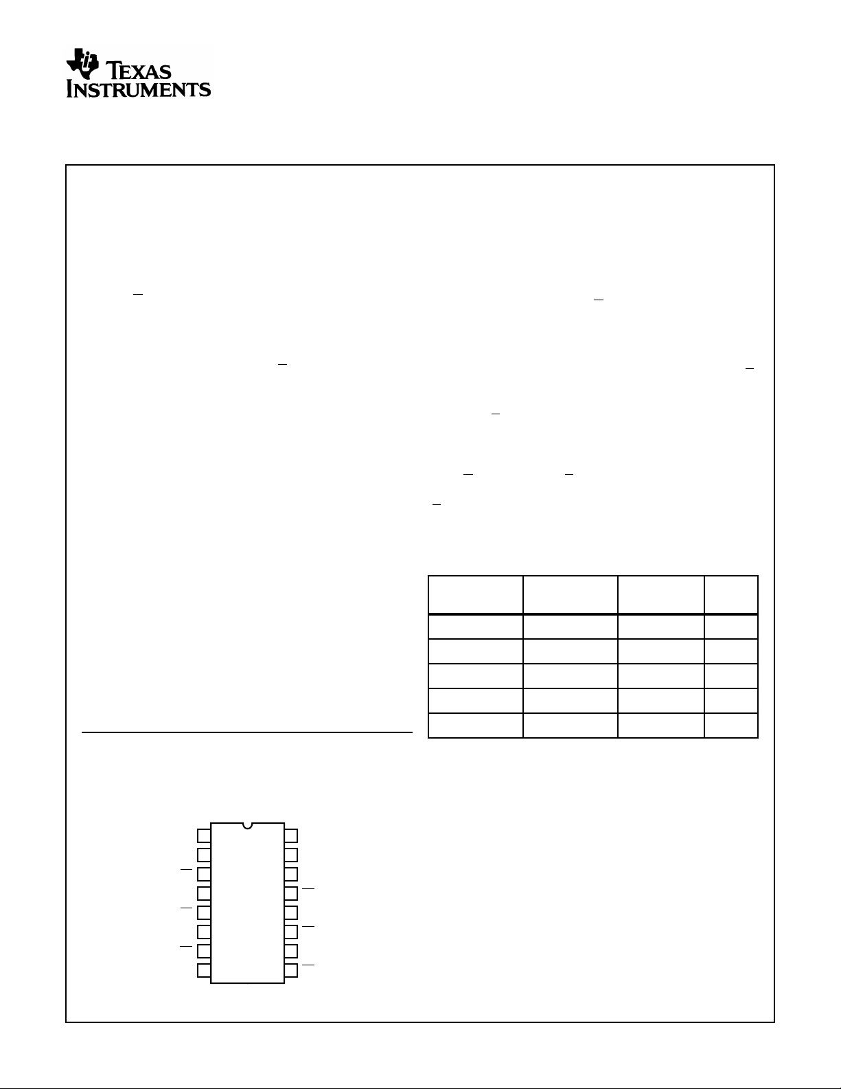
Pinout
CD54HC4538, CD74HC4538, CD74HCT4538
(PDIP, SOIC, CERDIP)
TOP VIEW
16
1C
1RXC
GND
1R
1A
1B
1Q
1Q
1
X
2
X
3
4
5
6
7
8
V
CC
15
2C
X
14
2RXC
X
13
2R
2A
12
11
2B
2Q
10
9
2Q
Description
The Harris CD54HC4538, CD74HC4538 and
CD74HCT4538 are dual retriggerable/resettable monostable
precision multivibrators for fixed voltage timing applications.
An external resistor (R
) and an external capacitor (CX)
X
control the timing and the accuracy for the circuit.
Adjustment of R
pulse widths from the Q and
and CXprovides a wide range of output
X
Q terminals. The propagation
delay from trigger input-to-output transition and the
propagation delay from reset input-to-output transition are
independent of R
Leading-edge triggering (A) and trailing edge triggering (
and CX.
X
B)
inputs are provided for triggering from either edge of the
input pulse. An unused “A” input should be tied to GND and
an unused
B should be tied to VCC. On power up the IC is
reset. Unused resets and sections must be terminated. In
normal operation the circuit retriggers on the application of
each new trigger pulse. To operate in the non-triggerable
mode
Q is connected to B when leading edge triggering (A)
is used or Q is connected to A when trailing edge triggering
(
B) is used. The period (τ) can be calculated from τ = (0.7)
R
, CX; R
X
is 5kΩ. C
MIN
MIN
is 0pF.
Ordering Information
TEMP. RANGE
PART NUMBER
CD54HC4538F -55 to 125 16 Ld CERDIP F16.3
CD74HC4538E -55 to 125 16 Ld PDIP E16.3
CD74HCT4538E -55 to 125 16 Ld PDIP E16.3
CD74HC4538M -55 to 125 16 Ld SOIC M16.15
CD74HCT4538M -55 to 125 16 Ld SOIC M16.15
NOTES:
1. When ordering, use the entire partnumber. Add the suffix 96 to
obtain the variant in the tape and reel.
2. Wafer anddie for thispart number isavailable which meets all
electrical specifications. Please contactyour local sales office or
Harris customer service for ordering information.
(oC) PACKAGE
PKG.
NO.
CAUTION: These devices are sensitive to electrostatic discharge. Users should follow proper IC Handling Procedures.
Copyright
© Harris Corporation 1998
1
File Number 1671.2
CD54HC4538, CD74HC4538, CD74HCT4538
Functional Diagram
4
1A
5
1B
3
1R
13
2R
12
2A
11
2B
GND = 8
= 16
V
CC
TRUTH TABLE
INPUTS OUTPUTS
RABQQ
1Cx 1Rx
12
1Cx 1RxCx
MONO 1
MONO 2
2Cx 2RxCx
15 14
2Cx 2Rx
CL
V
CC
6
1Q
7
1Q
10
2Q
9
2Q
V
CC
R2
R1
CL
Q
LXXLH
XHXLH
XXLLH
HL↓
H↑H
NOTE: H = High Level, L = Low Level, ↑ = Transition from Low to
High, ↓ = Transitionfrom High to Low, One High Level Pulse,
One Low Level Pulse, X = Irrelevant.
p
CL
n
CL
p
n
CL
Q
R1
D
CL
p
n
CL
FIGURE 1. FF DETAIL
2
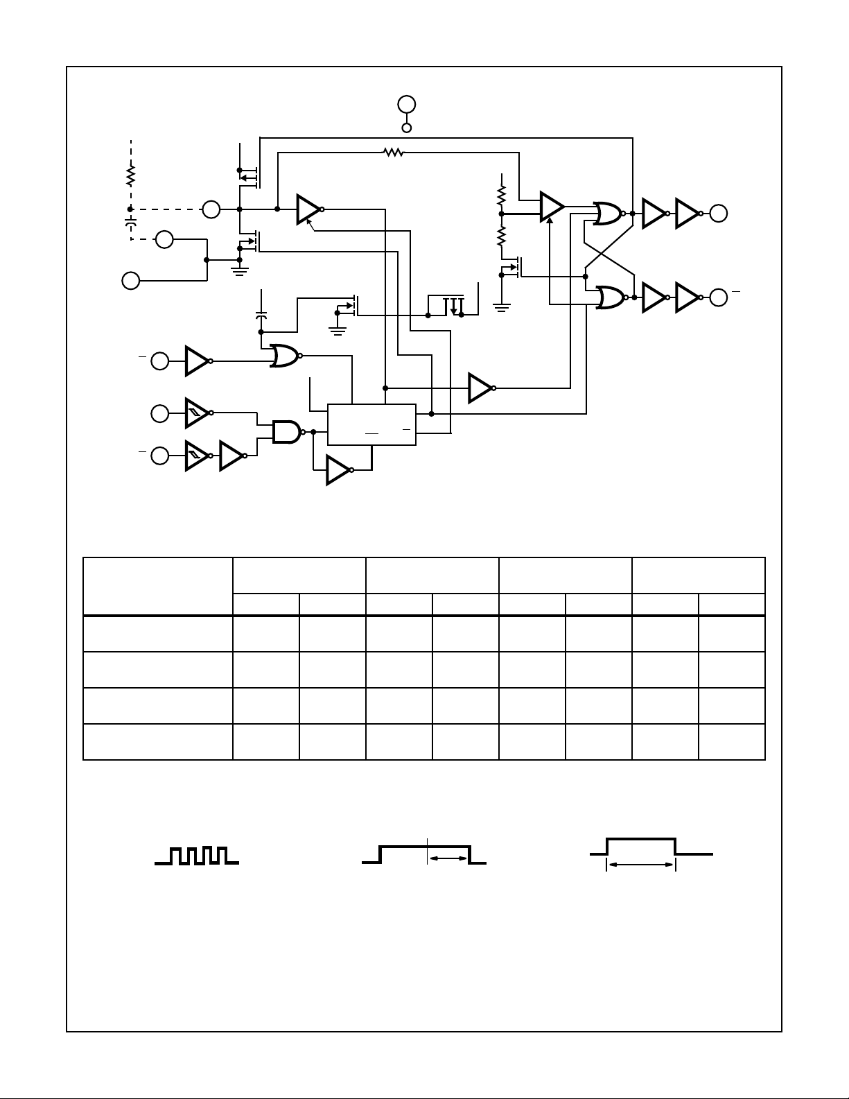
CD54HC4538, CD74HC4538, CD74HCT4538
16
V
CC
V
CC
COMP II
R1
+
-
R2
V
CC
Q
Q
6(10)
Q
7(9)
Q
2(14)
V
CC
V
CC
HIGH Z
V
CC
D
CL
R2R1
FF
CL
V
CC
R
X
C
1(15)
X
8
3(13)
R
4(12)
A
5(11)
B
FIGURE 2. LOGIC DIAGRAM (1 MONO)
FUNCTIONAL TERMINAL CONNECTIONS
FUNCTION
Leading-Edge
VCC TO
TERMINAL NUMBER
MONO
MONO
1
2
3, 5 11, 13 4 12
GND TO
TERMINAL NUMBER
MONO
MONO
1
INPUT PULSE TO
TERMINAL NUMBER
MONO
2
1
MONO
OTHER
CONNECTIONS
MONO
2
MONO
1
Trigger/Retriggerable
Leading-Edge
3 13 4 12 5-7 11-9
Trigger/Non-Retriggerable
Trailing-Edge
313412511
Trigger/Retriggerable
Trailing-Edge
3 13 5 11 4-6 12-10
Trigger/Non-Retriggerable
NOTES:
3. A retriggerable one-shot multivibrator has anoutput pulse width which is extended one full time period (T)after application of the last
trigger pulse.
4. A non-triggerable one-shot multivibrator has a time period (T) referenced from the application of the first trigger pulse.
T
FIGURE 3. INPUT PULSE TRAIN FIGURE 4. RETRIGGERABLE MODE
PULSE WIDTH (A MODE)
FIGURE5. NON-RETRIGGERABLEMODE
T
PULSE WIDTH
(A MODE)
2
3
CD54HC4538, CD74HC4538, CD74HCT4538
Absolute Maximum Ratings Thermal Information
DC Supply Voltage, VCC. . . . . . . . . . . . . . . . . . . . . . . . -0.5V to 7V
DC Input Diode Current, I
For VI < -0.5V or VI > VCC + 0.5V. . . . . . . . . . . . . . . . . . . . . .±20mA
DC Output Diode Current, I
For VO < -0.5V or VO > VCC + 0.5V . . . . . . . . . . . . . . . . . . . .±20mA
DC Output Source or Sink Current per Output Pin, I
For VO > -0.5V or VO < VCC + 0.5V . . . . . . . . . . . . . . . . . . . .±25mA
DC VCC or Ground Current, ICC . . . . . . . . . . . . . . . . . . . . . . . . .±50mA
IK
OK
O
Operating Conditions
Temperature Range, TA . . . . . . . . . . . . . . . . . . . . . . -55oC to 125oC
Supply Voltage Range, VCC (Note 5)
HC Types . . . . . . . . . . . . . . . . . . . . . . . . . . . . . . . . . . . . .2V to 6V
HCT Types . . . . . . . . . . . . . . . . . . . . . . . . . . . . . . . . .4.5V to 5.5V
DC Input or Output Voltage, VI, VO . . . . . . . . . . . . . . . . . 0V to V
Input Rise and Fall Times, tr, t
Reset Input:
2V . . . . . . . . . . . . . . . . . . . . . . . . . . . . . . . . . . . . . . 1000ns (Max)
4.5V. . . . . . . . . . . . . . . . . . . . . . . . . . . . . . . . . . . . . . 500ns (Max)
6V . . . . . . . . . . . . . . . . . . . . . . . . . . . . . . . . . . . . . . . 400ns (Max)
Trigger Inputs A or B:
2V . . . . . . . . . . . . . . . . . . . . . . . . . . . . . . . . . . . . .Unlimited (Max)
4.5V. . . . . . . . . . . . . . . . . . . . . . . . . . . . . . . . . . . .Unlimited (Max)
6V . . . . . . . . . . . . . . . . . . . . . . . . . . . . . . . . . . . . .Unlimited (Max)
External Timing Resistor, RX (Note 6) . . . . . . . . . . . . . . . .5kΩ (Min)
External Timing Capacitor, CX (Note 6) . . . . . . . . . . . . . . . . .0 (Min)
CAUTION: Stresses above those listed in “Absolute Maximum Ratings” may cause permanent damage to the device. This is a stress only rating and operation
of the device at these or any other conditions above those indicated in the operational sections of this specification is not implied.
NOTES:
5. Unless otherwise specified, all voltages are referenced to ground.
6. The maximumallowable values of RXand CXare afunction of leakage of capacitor CX, theleakage of the HC4538, and leakage due to
board layout and surface resistance. Values of RXand CXshould be chosen so that the maximum current into pin 2 or pin 14 is 30mA.
Susceptibility to externally induced noise signals may occur for RX > 1MΩ.
7. θJA is measured with the component mounted on an evaluation PC board in free air.
f
Thermal Resistance (Typical, Note 7) θJA (oC/W) θJC (oC/W)
PDIP Package. . . . . . . . . . . . . . . . . . . 90 N/A
SOIC Package. . . . . . . . . . . . . . . . . . . 160 N/A
CERDIP Package . . . . . . . . . . . . . . . . 130 55
Maximum Junction Temperature. . . . . . . . . . . . . . . . . . . . . . .150oC
Maximum Storage Temperature Range . . . . . . . . . .-65oC to 150oC
Maximum Lead Temperature (Soldering 10s). . . . . . . . . . . . .300oC
(SOIC - Lead Tips Only)
CC
DC Electrical Specifications
PARAMETER SYMBOL
HC TYPES
High Level Input
Voltage
Low Level Input
Voltage
High Level Output
Voltage
CMOS Loads
High Level Output
Voltage
TTL Loads
V
IH
V
IL
V
OH
TEST
CONDITIONS
(V) IO(mA) MIN TYP MAX MIN MAX MIN MAX
I
- - 2 1.5 - - 1.5 - 1.5 - V
- - 2 - - 0.5 - 0.5 - 0.5 V
VIHor VIL-0.02 2 1.9 - - 1.9 - 1.9 - V
-0.02 4.5 4.4 - - 4.4 - 4.4 - V
-0.02 6 5.9 - - 5.9 - 5.9 - V
-4 4.5 3.98 - - 3.84 - 3.7 - V
-5.2 6 5.48 - - 5.34 - 5.2 - V
V
CC
(V)
4.5 3.15 - - 3.15 - 3.15 - V
6 4.2 - - 4.2 - 4.2 - V
4.5 - - 1.35 - 1.35 - 1.35 V
6 - - 1.8 - 1.8 - 1.8 V
- - ---- - - - V
o
C -40oC TO 85oC -55oCTO125oC
25
UNITSV
4

CD54HC4538, CD74HC4538, CD74HCT4538
DC Electrical Specifications (Continued)
TEST
PARAMETER SYMBOL
Low Level Output
Voltage
CMOS Loads
CONDITIONS
(V) IO(mA) MIN TYP MAX MIN MAX MIN MAX
I
V
VIHor VIL0.02 2 - - 0.1 - 0.1 - 0.1 V
OL
0.02 4.5 - - 0.1 - 0.1 - 0.1 V
V
CC
(V)
0.02 6 - - 0.1 - 0.1 - 0.1 V
Low Level Output
Voltage
TTL Loads
- - ---- - - - V
4 4.5 - - 0.26 - 0.33 - 0.4 V
5.2 6 - - 0.26 - 0.33 - 0.4 V
Input Leakage
Current A,
B, R
Input Leakage
Current R
XCX
I
VCC or
I
-6--±0.1 - ±1-±1µA
GND
-6--±0.05 - ±0.5 - ±0.5 µA
(Note 9)
Quiescent Device
Current
Active Device Current
Q =High & Pins2, 14
at V
/4
CC
I
I
CC
CC
VCC or
GND
VCC or
GND
0 6 - - 8 - 80 - 160 µA
0 6 - - 0.6 - 0.8 - 1 mA
HCT TYPES
High Level Input
Voltage
Low Level Input
Voltage
High Level Output
Voltage
V
IH
- - 4.5 to
2--2- 2 - V
5.5
V
IL
- - 4.5 to
- - 0.8 - 0.8 - 0.8 V
5.5
V
VIHor VIL-0.02 4.5 4.4 - - 4.4 - 4.4 - V
OH
CMOS Loads
High Level Output
-4 4.5 3.98 - - 3.84 - 3.7 - V
Voltage
TTL Loads
Low Level Output
Voltage
V
VIHor VIL0.02 4.5 - - 0.1 - 0.1 - 0.1 V
OL
CMOS Loads
Low Level Output
4 4.5 - - 0.26 - 0.33 - 0.4 V
Voltage
TTL Loads
Input Leakage
Current
Input Leakage
Current R
XCX
I
VCCand
I
- 5.5 - ±0.1 - ±1-±1µA
GND
- 5.5 - - ±0.05 - ±0.5 - ±0.5 µA
(Note 9)
Quiescent Device
Current
Active Device Current
Q =High & Pins2, 14
at V
/4
CC
Additional Quiescent
Device Current Per
I
CC
I
CC
∆I
CC
(Note 8)
VCC or
GND
VCC or
GND
V
CC
-2.1
0 5.5 - - 8 - 80 - 160 µA
0 5.5 - - 0.6 - 0.8 - 1 mA
- 4.5 to
- 100 360 - 450 - 490 µA
5.5
Input Pin: 1 Unit Load
NOTES:
8. For dual-supply systems theoretical worst case (V
= 2.4V, VCC = 5.5V) specification is 1.8mA.
I
9. When testingIILthe Qoutput must behigh. If Qis low (device not triggered) the pull-up P device will be ON and the low resistance path
from VDD to the test pin will cause a current far exceeding the specification.
o
C -40oC TO 85oC -55oCTO125oC
25
UNITSV
5

CD54HC4538, CD74HC4538, CD74HCT4538
HCT Input Loading Table
INPUT UNIT LOADS
All 0.5
NOTE: Unit Load is ∆ICClimit specified in DC Electrical Table, e.g.
360µA max at 25oC.
Prerequisite for Switching Specifications
25oC -40oC TO 85oC -55oC TO 125oC
PARAMETER SYMBOL VCC(V)
HC TYPES
Input Pulse Widths tWH, t
A, B 2 80 - - 100 - - 120 - - ns
Rt
Reset Recovery Time t
Retrigger Time
(Figure 11)
HCT TYPES
Input Pulse Widths tWH, t
A, B 4.5 16 - - 20 - - 24 - - ns
Rt
Reset Recovery Time t
Retrigger Time
(Figure 11)
WL
REC
t
rr
WL
REC
t
rr
WL
4.5 16 - - 20 - - 24 - - ns
614- -17- -20--ns
2 80 - - 100 - - 120 - - ns
4.5 16 - - 20 - - 24 - - ns
614- -17- -20--ns
25--5--5--ns
4.5 5 - - 5 - - 5 - - ns
65--5--5--ns
5 - 175 - - - - - - - ns
WL
4.5 20 - - 25 - - 30 - - ns
4.5 5 - - 5 - - 5 - - ns
5 - 175 - - - - - - - ns
UNITSMIN TYP MAX MIN TYP MAX MIN TYP MAX
6

CD54HC4538, CD74HC4538, CD74HCT4538
Switching Specifications C
PARAMETER SYMBOL
= 50pF, Input tr, tf= 6ns, RX = 10KΩ, CX = 0
L
TEST
CONDITIONS V
CC
(V)
25oC
-40oC TO
85oC
-55oC TO
125oC
HC TYPES
Propagation Delay t
PLH
CL = 50pF
A, B to Q 2 - - 250 - 315 - 375 ns
4.5 - - 50 - 63 - 75 ns
CL = 15pF 5 - 21 - - - - - ns
CL = 50pF 6 - - 43 - 54 - 64 ns
A, B to Qt
PHL
CL = 50pF 2 - - 250 - 315 - 375 ns
4.5 - - 50 - 63 - 75 ns
CL = 15pF 5 - 21 - - - - - ns
CL = 50pF 6 - - 43 - 54 - 64 ns
R to Q t
PHL
CL = 50pF 2 - - 250 - 315 - 375 ns
4.5 - - 50 - 63 - 75 ns
CL = 15pF 5 - 21 - - - - - ns
UNITSMIN TYP MAX MIN MAX MIN MAX
CL = 50pF 6 - - 43 - 54 - 64 ns
R to Qt
PLH
CL = 50pF 2 - - 250 - 315 - 375 ns
4.5 - - 50 - 63 - 75 ns
CL = 15pF 5 - 21 - - - - - ns
CL = 50pF 6 - - 43 - 54 - 64 ns
Output Transition Time t
TLH
, t
CL = 50pF 2 - - 75 - 95 - 110 ns
THL
4.5 - - 15 - 19 - 22 ns
6 - - 13 - 16 - 19 ns
Output Pulse Width
τ
CL = 50pF 3 0.64 - 0.78 0.612 0.812 0.605 0.819 ms
RX = 10k, CX = 0.1µF
5 0.63 - 0.77 0.602 0.798 0.595 0.805 ms
Output Pulse Width Match,
-- -±1- - - - - %
Same Package
Power Dissipation Capacitance C
Input Capacitance C
PD
I
CL = 15pF 5 - 136 - - - - - pF
CL = 50pF - 10 - 10 - 10 - 10 pF
HCT TYPES
Propagation Delay t
PLH
A, B to Q CL = 50pF 4.5 - - 55 - 69 - 83 ns
CL = 15pF 5 - 23 - - - - - ns
A, B to Qt
PHL
CL = 50pF 4.5 - - 55 - 69 - 83 ns
CL = 15pF 5 - 23 - - - - - ns
R to Q t
PHL
CL = 50pF 4.5 - - 40 - 50 - 60 ns
CL = 15pF 5 - 17 - - - - - ns
7
CD54HC4538, CD74HC4538, CD74HCT4538
Switching Specifications C
= 50pF, Input tr, tf= 6ns, RX = 10KΩ, CX = 0 (Continued)
L
TEST
PARAMETER SYMBOL
R to Qt
PLH
CONDITIONS V
CC
(V)
CL = 50pF 4.5 - - 50 - 63 - 75 ns
CL = 15pF 5 - 21 - - - - - ns
Output Transition Time t
Output Pulse Width
TLH
, t
τ
CL = 50pF 4.5 - - 15 - 19 - 22 ns
THL
CL = 50pF 5 0.63 - 0.77 0.602 0.798 0.595 0.805 ms
RX = 10k, CX = 0.1µF
Output Pulse Width Match,
----±1- - - - - %
Same Package
Power Dissipation Capacitance C
Input Capacitance C
PD
I
CL = 15pF 5 - 134 - - - - - pF
CL = 50pF - 10 - 10 - 10 - 10 pF
NOTES:
10. CPD is used to determine the dynamic power consumption, per one shot.
11. PD=(CPD+CX)V
CC
2
fi∑(CLV
CX = external capacitance VCC = supply voltage assuming fi «
2
fO) where fi= input frequency, fO= output frequency, CL= output load capacitance,
CC
I
--
τ
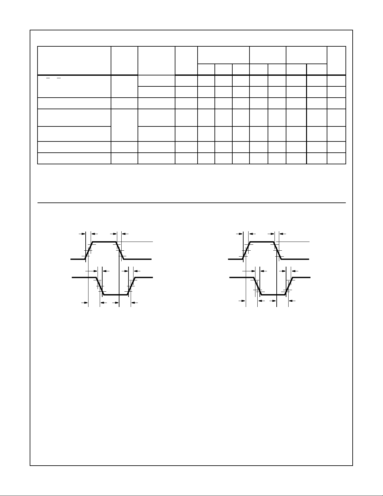
Test Circuits and Waveforms
25oC
-40oC TO
85oC
-55oC TO
125oC
UNITSMIN TYP MAX MIN MAX MIN MAX
tr = 6ns tf = 6ns
V
t
CC
GND
TLH
INPUT
t
INVERTING
OUTPUT
THL
t
PHL
90%
50%
10%
t
90%
50%
10%
PLH
FIGURE 6. HC AND HCU TRANSITION TIMES ANDPROPAGA-
TION DELAY TIMES, COMBINATION LOGIC
= 6ns
t
PLH
t
f
1.3V
10%
90%
t
TLH
3V
GND
tr = 6ns
INPUT
t
INVERTING
OUTPUT
THL
t
PHL
2.7V
1.3V
0.3V
FIGURE 7. HCT TRANSITION TIMES AND PROPAGATION
DELAY TIMES, COMBINATION LOGIC
8

CD54HC4538, CD74HC4538, CD74HCT4538
Typical Performance Curves
0.70
0.69
K FACTOR
0.68
0.67
2 3 4 4.5 5 5.5 6
, DC SUPPLY VOLTAGE (V)
V
CC
HC4538 - TA11646C
= 25oC
T
A
10kΩ, 10nF
10kΩ, 100nF
100kΩ, 100nF
100kΩ, 10nF
0.70
0.69
K FACTOR
0.68
0.67
2 3 4 4.5 5 5.5 6
, DC SUPPLY VOLTAGE (V)
V
CC
HCT4538 - TA13646C
= 25oC
T
A
10kΩ, 10nF
10kΩ, 100nF
100kΩ, 100nF
100kΩ, 10nF
FIGURE 8. K FACTOR vs DC SUPPLY VOLTAGE (VCC) - V FIGURE 9. K FACTOR vs DC SUPPLY VOLTAGE (VCC) - V
4
10
3
10
2
10
, TYP MIN RETRIGGER TIME (ns)
rr
t
10
VCC = 4.5V
VCC = 5V
2
10
CX, TIMING CAPACITANCE (pF)
TA = 25oC
= 10kΩ
R
X
3
10
K FACTOR
1.3
1.2
1.1
1.0
0.9
0.8
0.7
0.6
HC/HCT4538
V
= 5V, TA = 25oC
CC
2kΩ
10kΩ
100kΩ
2
10
10
CX, TIMING CAPACITANCE (pF)
3
10
4
10
5
10
4
10
FIGURE 10. K FACTOR vs C
X
FIGURE 11. MINIMUM RETRIGGER TIME vs TIMING
CAPACITANCE
9
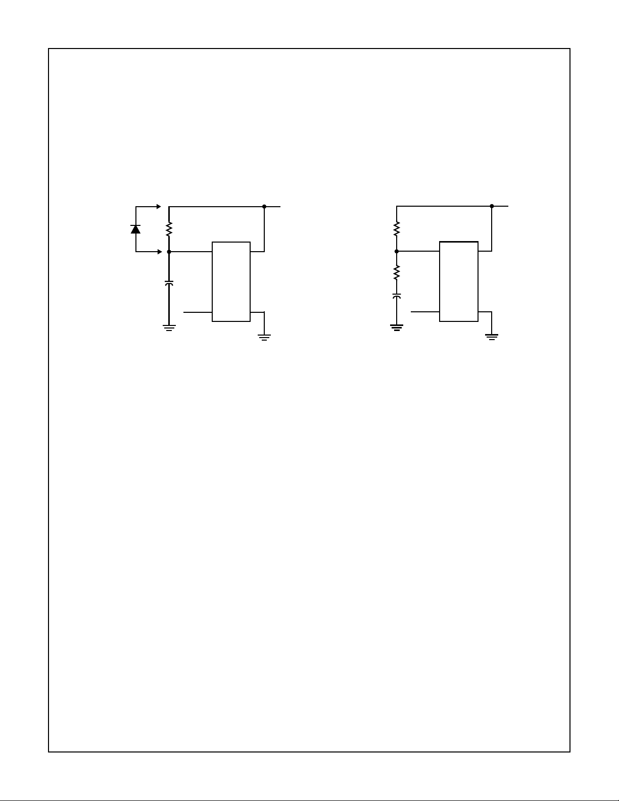
Power-Down Mode
CD54HC4538, CD74HC4538, CD74HCT4538
During a rapid power-down condition, as would occur with a
power-supply short circuit with apoorly filtered power supply,
the energy stored in C
aviod possible device damage in this mode, when C
could discharge into Pin 2 or 14. To
X
X
is ≥
0.5µF, a protection diode with a 1 ampere or higher rating
(1N5395 or equivalent) and a separate ground return for C
should be provided as shown in Figure 12.
V
CC
IN5395
EQUIVALENT
OR
FIGURE 12. RAPID POWER-DOWN PROTECTION CIRCUIT
C
≥0.5µF
R
X
2(14)
+
X
1(15)
16
8
An alternate protection method is shown in Figure 13, where
a51Ωcurrent-limiting resistor is inserted in series with C
Note that a small pulse width decrease will occur however,
and R
must be appropriately increased to obtain the origi-
X
nally desired pulse width.
X
V
CC
R
X
2(14)
51Ω
C
X
≥0.5µF
1(15)
FIGURE 13. ALTERNATE RAPID POWER-DOWN PROTECTION
CIRCUIT
16
8
.
X
10

IMPORTANT NOTICE
T exas Instruments and its subsidiaries (TI) reserve the right to make changes to their products or to discontinue
any product or service without notice, and advise customers to obtain the latest version of relevant information
to verify, before placing orders, that information being relied on is current and complete. All products are sold
subject to the terms and conditions of sale supplied at the time of order acknowledgement, including those
pertaining to warranty, patent infringement, and limitation of liability.
TI warrants performance of its semiconductor products to the specifications applicable at the time of sale in
accordance with TI’s standard warranty. Testing and other quality control techniques are utilized to the extent
TI deems necessary to support this warranty . Specific testing of all parameters of each device is not necessarily
performed, except those mandated by government requirements.
CERT AIN APPLICATIONS USING SEMICONDUCTOR PRODUCTS MAY INVOLVE POTENTIAL RISKS OF
DEATH, PERSONAL INJURY, OR SEVERE PROPERTY OR ENVIRONMENTAL DAMAGE (“CRITICAL
APPLICATIONS”). TI SEMICONDUCTOR PRODUCTS ARE NOT DESIGNED, AUTHORIZED, OR
WARRANTED TO BE SUITABLE FOR USE IN LIFE-SUPPORT DEVICES OR SYSTEMS OR OTHER
CRITICAL APPLICA TIONS. INCLUSION OF TI PRODUCTS IN SUCH APPLICATIONS IS UNDERST OOD TO
BE FULLY AT THE CUSTOMER’S RISK.
In order to minimize risks associated with the customer’s applications, adequate design and operating
safeguards must be provided by the customer to minimize inherent or procedural hazards.
TI assumes no liability for applications assistance or customer product design. TI does not warrant or represent
that any license, either express or implied, is granted under any patent right, copyright, mask work right, or other
intellectual property right of TI covering or relating to any combination, machine, or process in which such
semiconductor products or services might be or are used. TI’s publication of information regarding any third
party’s products or services does not constitute TI’s approval, warranty or endorsement thereof.
Copyright 1999, Texas Instruments Incorporated
 Loading...