Texas Instruments CD74HCT238M, CD74HCT238E, CD74HCT138M96, CD74HCT138M, CD74HCT138E Datasheet
...
CD74HC138, CD74HCT138,
/
j
[ /Title
(CD74
HC138
,
CD74
HCT13
8,
CD74
HC238
,
CD74
HCT23
8)
Subect
(High
Speed
Data sheet acquired from Harris Semiconductor
SCHS147A
October 1997 - Revised February 1999
Features
• Select One Of Eight Data Outputs
Active Low for 138, Active High for 238
• l/O Port or Memory Selector
• Three Enable Inputs to Simplify Cascading
• Typical Propagation Delay of 13ns at V
C
= 15pF, TA = 25oC
L
• Fanout (Over Temperature Range)
- Standard Outputs. . . . . . . . . . . . . . . 10 LSTTL Loads
- Bus Driver Outputs . . . . . . . . . . . . . 15 LSTTL Loads
• Wide Operating Temperature Range . . . -55
• Balanced Propagation Delay and Transition Times
• Significant Power Reduction Compared to LSTTL
Logic ICs
• HC Types
- 2V to 6V Operation
- High Noise Immunity: N
at VCC = 5V
• HCT Types
- 4.5V to 5.5V Operation
- Direct LSTTL Input Logic Compatibility,
V
= 0.8V (Max), VIH = 2V (Min)
IL
- CMOS Input Compatibility, I
= 30%, NIH = 30% of V
IL
≤ 1µA at VOL, V
l
CC
= 5V,
o
CD74HC238, CD74HCT238
High Speed CMOS Logic 3-to-8 Line Decoder/
Demultiplexer Inverting and Non-Inverting
C to 125oC
CC
OH
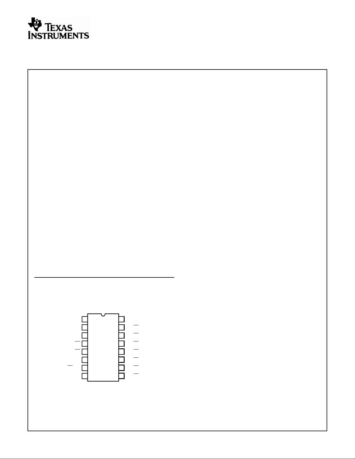
Pinout
CD74HC138, CD74HCT138, CD74HC238, CD74HCT238
(PDIP, SOIC)
TOP VIEW
V
1
A0
A1
2
A2
3
4
E1
5
E2
E3
6
GND
7
8
(Y7) Y7
Signal names in parentheses are for ’HC238 and ’HCT238.
CAUTION: These devices are sensitive to electrostatic discharge. Users should follow proper IC Handling Procedures.
Copyright
© 1999, Texas Instruments Incorporated
16
15
14
13
12
11
10
9
CC
Y0)
Y0 (
Y1 (Y1)
Y2 (Y2)
Y3 (Y3)
Y4 (
Y4)
Y5)
Y5 (
Y6 (
Y6)
1

CD74HC138, CD74HCT138, CD74HC238, CD74HCT238
Description
The Harris CD74HC138, CD74HC238 and CD74HCT138,
CD74HCT238 are high speed silicon gate CMOS decoders
well suited to memory address decoding or data routing
applications. Both circuits feature low power consumption
usually associated with CMOS circuitry, yet have speeds
comparable to low power Schottky TTL logic. Both circuits
have three binary select inputs(A0, A1 and A2). If the device
is enabled, these inputs determine which one of the eight
normally high outputs of the HC/HCT138 series will go low
or which of the normally low outputs of the HC/HCT238
series will go high.
Two active low and one active high enables (
E1, E2, and E3)
are provided to ease the cascading of decoders. The
decoder’s 8 outputs can drive 10 low power Schottky TTL
equivalent loads.
Ordering Information
PKG.
PART NUMBER TEMP. RANGE (oC) PACKAGE
CD74HC138E -55 to 125 16 Ld PDIP E16.3
NO.
Ordering Information
PKG.
PART NUMBER TEMP. RANGE (oC) PACKAGE
CD74HCT138E -55 to 125 16 Ld PDIP E16.3
CD74HC238E -55 to 125 16 Ld PDIP E16.3
CD74HCT238E -55 to 125 16 Ld PDIP E16.3
CD74HC138M -55 to 125 16 Ld SOIC M16.15
CD74HCT138M -55 to 125 16 Ld SOIC M16.15
CD74HC238M -55 to 125 16 Ld SOIC M16.15
CD74HCT238M -55 to 125 16 Ld SOIC M16.15
CD74HC138SM -55 to 125 16 Ld SSOP M16.209
NOTES:
1. When ordering, use the entire partnumber. Add the suffix 96 to
obtain the variant in the tape and reel.
2. Wafer and die for this part number is available which meets all
electrical specifications. Please contact your local sales office or
Harris customer service for ordering information.
NO.
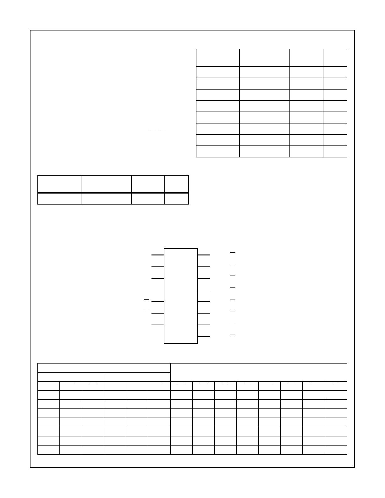
Functional Diagram
HC/HCT
HC/HCT
238
Y1
Y2
Y3
Y4
Y5
Y6
Y7
138
Y0
Y1
Y2
Y3
Y4
Y5
Y6
Y7
OUTPUTSENABLE ADDRESS
1
A0 Y0
2
A1
3
A2
4
E1
5
E2
6
E3
15
14
13
12
11
10
9
7
TRUTH TABLE CD74HC138, CD74HCT138
INPUTS
E3 E2 E1 A2 A1 A0 Y0 Y1 Y2 Y3 Y4 Y5 Y6 Y7
XXHXXXHHHHHHHH
LXXXXXHHHHHHHH
XHXXXXHHHHHHHH
HLLLLLLHHHHHHH
HLLLLHHLHHHHHH
HLLLHLHHLHHHHH
HL LLHHHHHLHHHH
2

CD74HC138, CD74HCT138, CD74HC238, CD74HCT238
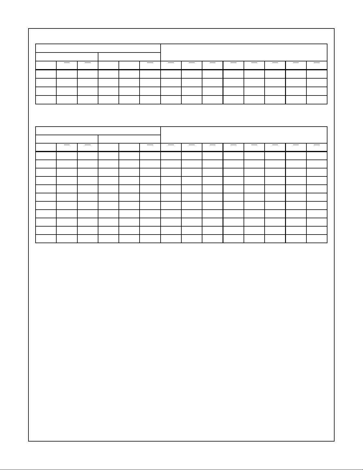
TRUTH TABLE CD74HC138, CD74HCT138
INPUTS
OUTPUTSENABLE ADDRESS
E3
HLLHLLHHHHLHHH
HLLHLHHHHHHLHH
HLLHHLHHHHHHLH
HLLHHHHHHHHHHL
NOTE: H = High Voltage Level, L = Low Voltage Level, X = Don’t Care
E3
XXHXXXLLLLLLLL
LXXXXXLLLLLLLL
XHXXXXLLLLLLLL
HLLLLLHLLLLLLL
HLLLLHLHLLLLLL
HLLLHLLLHLLLLL
HLLLHHLLLHLLLL
HLLHLLLLLLHLLL
HLLHLHLLLLLHLL
HLLHHLLLLLLLHL
HLLHHHLLLLLLLH
NOTE: H = High Voltage Level, L = Low Voltage Level, X = Don’t Care
E2 E1 A2 A1 A0 Y0 Y1 Y2 Y3 Y4 Y5 Y6 Y7
TRUTH TABLE CD74HC238, CD74HCT238
INPUTS
OUTPUTSENABLE ADDRESS
E2 E1 A2 A1 A0 Y0 Y1 Y2 Y3 Y4 Y5 Y6 Y7
3
 Loading...