

Texas Instruments CD74HCT4316M96, CD74HCT4316M, CD74HCT4316E, CD74HC4316PWR, CD74HC4316M96 Datasheet
...
CD74HC4316,
/
j
[ /Title
(CD74
HC431
6,
CD74
HCT43
16)
Subect
(HighSpeed
CMOS
Data sheet acquired from Harris Semiconductor
SCHS212
February 1998
Features
• Wide Analog-Input-Voltage Range
V
- VEE . . . . . . . . . . . . . . . . . . . . . . . . . . . . .0V to 10V
CC
• Low “ON” Resistance
-45Ω (Typ). . . . . . . . . . . . . . . . . . . . . . . . . . .V
-35Ω (Typ). . . . . . . . . . . . . . . . . . . . . . . . . . . . V
-30Ω (Typ). . . . . . . . . . . . . . . . . . . . . . . V
• Fast Switching and Propagation Delay Times
• Low “OFF” Leakage Current
• Built-In “Break-Before-Make” Switching
• Logic-Level Translation to Enable 5V Logic to
Accommodate ±5V Analog Signals
• Wide Operating Temperature Range . . . -55
• HC Types
- 2V to 10V Operation
- High Noise Immunity: N
at VCC = 5V
• HCT Types
- Direct LSTTL Input Logic Compatibility,
V
= 0.8V (Max), VIH = 2V (Min)
IL
- CMOS Input Compatibility, I
= 30%, NIH = 30% of V
IL
≤ 1µA at VOL, V
l
CC
CC
- VEE = 9V
CC
o
C to 125oC
OH
CD74HCT4316
High-Speed CMOS Logic
Quad Analog Switch with Level Translation
Description
The Harris CD74HC4316 and CD74HCT4316 contains four
independent digitally controlled analog switches that use
silicon-gate CMOS technology to achieve operating speeds
= 4.5V
= 6V
similar to LSTTL with the low power consumption of
standard CMOS integrated circuits.
In addition these devices contain logic-level translation
circuits that provide for analog signal switching of voltages
between ±5V via 5V logic. Each switch is turned on by a
high-level voltage on its select input (S) when the common
Enable (E) is Low. A High E disables all switches. The digital
inputs can swing between V
inputs/outputs can swing between V
and V
Figures 2 and 3.
as a negative limit. Voltage ranges are shown in
EE
and GND; the analog
CC
as a positive limit
CC
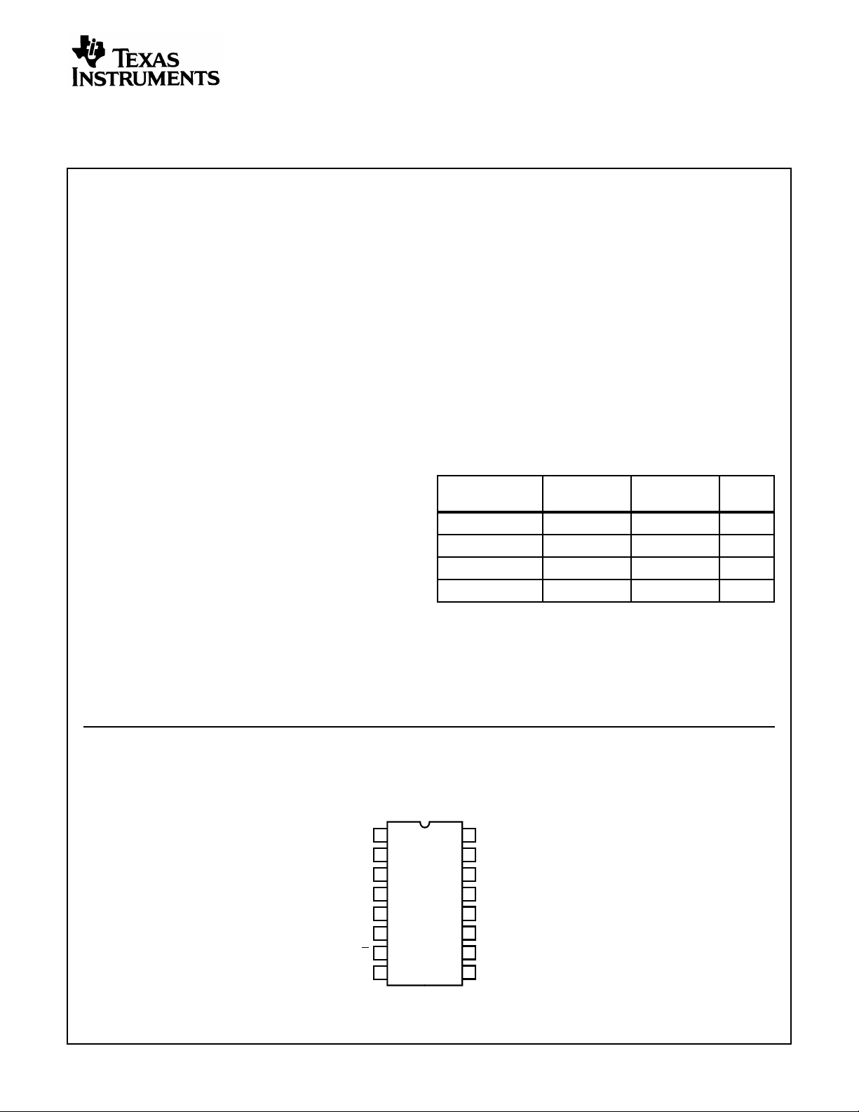
Ordering Information
TEMP. RANGE
CC
PART NUMBER
CD74HC4316E -55 to 125 16 Ld PDIP E16.3
CD74HCT4316E -55 to 125 16 Ld PDIP E16.3
CD74HC4316M -55 to 125 16 Ld SOIC M16.15
CD74HCT4316M -55 to 125 16 Ld SOIC M16.15
NOTES:
1. When ordering, use the entire part number. Add the suffix 96 to
obtain the variant in the tape and reel.
2. Wafer and die is available which meets all electrical
specifications. Please contact your local sales office or Harris
customer service for ordering information.
(oC) PACKAGE
PKG.
NO.
Pinout
CD74HC4316, CD74HCT4316
(PDIP, SOIC)
TOP VIEW
V
1
1Z
2
1Y
2Y
3
2Z
4
5
2S
3S
6
7
E
GND
8
CAUTION: These devices are sensitive to electrostatic discharge. Users should follow proper IC Handling Procedures.
Copyright
© Harris Corporation 1998
16
CC
15
1S
14
4S
13
4Z
12
4Y
3Y
11
10
3Z
V
9
EE
1
File Number 1916.1
Functional Diagram
CD74HC4316, CD74HCT4316CD74HC4316, CD74HCT4316
15
1S
5
2S
6
3S
14
4S
7
E
INPUTS
L L OFF
LHON
H X OFF
NOTE:
H = High Level Voltage
L = Low Level Voltage
X = Don’t Care
V
CC
16
LOGIC
LEVEL
CONV.
AND
CONTROL
89
GND
V
EE
TRUTH TABLE
2
1Y
1
1Z
3
2Y
4
2Z
11
3Y
10
3Z
12
4Y
13
4Z
SWITCHES
Logic Diagram
E
nS
TO 3 OTHER
SWITCHES
V
CC
LOGIC
LEVEL
CONV.
V
EE
FIGURE 1. ONE SWITCH
nY
V
CC
nZ
V
EE
2
CD74HC4316, CD74HCT4316CD74HC4316, CD74HCT4316
Absolute Maximum Ratings Thermal Information
DC Supply Voltage, VCC. . . . . . . . . . . . . . . . . . . . . . . . -0.5V to 7V
DC Supply Voltage, V
CC - VEE
. . . . . . . . . . . . . . . . . . -0.5V to 10.5V
DC Supply Voltage, VEE . . . . . . . . . . . . . . . . . . . . . . . . 0.5V to -7V
DC Input Diode Current, I
IK
For VI < -0.5V or VI > VCC 0.5V. . . . . . . . . . . . . . . . . . . . . . . .±20mA
DC Switch Diode Current, I
OK
For VI < VEE -0.5V or VI < VCC + 0.5V . . . . . . . . . . . . . . . . .±25mA
DC Switch Diode Current
For VI > VEE -0.5V or VI < VCC + 0.5V . . . . . . . . . . . . . . . . .±25mA
DC Output Diode Current, I
OK
For VO < -0.5V or VO > VCC + 0.5V . . . . . . . . . . . . . . . . . . . .±20mA
DC Output Source or Sink Current per Output Pin, I
O
For VO > -0.5V or VO < VCC + 0.5V . . . . . . . . . . . . . . . . . . . .±25mA
DC VCC or Ground Current, ICC . . . . . . . . . . . . . . . . . . . . . . . . .±50mA
Operating Conditions
Temperature Range, TA . . . . . . . . . . . . . . . . . . . . . . -55oC to 125oC
Supply Voltage Range, V
HC Types . . . . . . . . . . . . . . . . . . . . . . . . . . . . . . . . . . . . .2V to 6V
HCT Types . . . . . . . . . . . . . . . . . . . . . . . . . . . . . . . . .4.5V to 5.5V
Supply Voltage Range, V
HC, HCT Types (Figure 2) . . . . . . . . . . . . . . . . . . . . . . .2V to 10V
Supply Voltage Range, V
HC, HCT Types (Figure 3) . . . . . . . . . . . . . . . . . . . . . . . 0V to -6V
DC Input or Output Voltage, VI. . . . . . . . . . . . . . . . . . . GND to V
Analog Switch I/O Voltage, VIS. . . . . . . . . . . . . . . . . . . . . VEE (Min)
. . . . . . . . . . . . . . . . . . . . . . . . . . . . . . . . . . . . . . . . . . .VCC (Max)
Input Rise and Fall Time, tr, t
2V . . . . . . . . . . . . . . . . . . . . . . . . . . . . . . . . . . . . . . 1000ns (Max)
4.5V. . . . . . . . . . . . . . . . . . . . . . . . . . . . . . . . . . . . . . 500ns (Max)
6V . . . . . . . . . . . . . . . . . . . . . . . . . . . . . . . . . . . . . . . 400ns (Max)
CAUTION: Stresses above those listed in “Absolute Maximum Ratings” may cause permanent damage to the device. This is a stress only rating and operation
of the device at these or any other conditions above those indicated in the operational sections of this specification is not implied.
NOTE:
3. θJA is measured with the component mounted on an evaluation PC board in free air.
CC
CC -VEE
EE
f
Thermal Resistance (Typical, Note 3) θJA (oC/W)
PDIP Package. . . . . . . . . . . . . . . . . . . . . . . . . . . . . 90
SOICSC Package . . . . . . . . . . . . . . . . . . . . . . . . . . 115
Maximum Junction Temperature (Plastic Package) . . . . . . . . 150oC
Maximum Storage Temperature Range . . . . . . . . . .-65oC to 150oC
Maximum Lead Temperature (Soldering 10s) . . . . . . . . . . . . . 300oC
CC
Recommended Operating Area as a Function of Supply Voltage
8
(V)
6
HC
4
2
0
024681012
V
- VEE (V)
CC
HCT
FIGURE 2. FIGURE 3.
VCC - GND
VCC - GND
(V)
8
6
4
2
0
0-2-4-6-8
V
EE
HCT
- GND (V)
HC
3
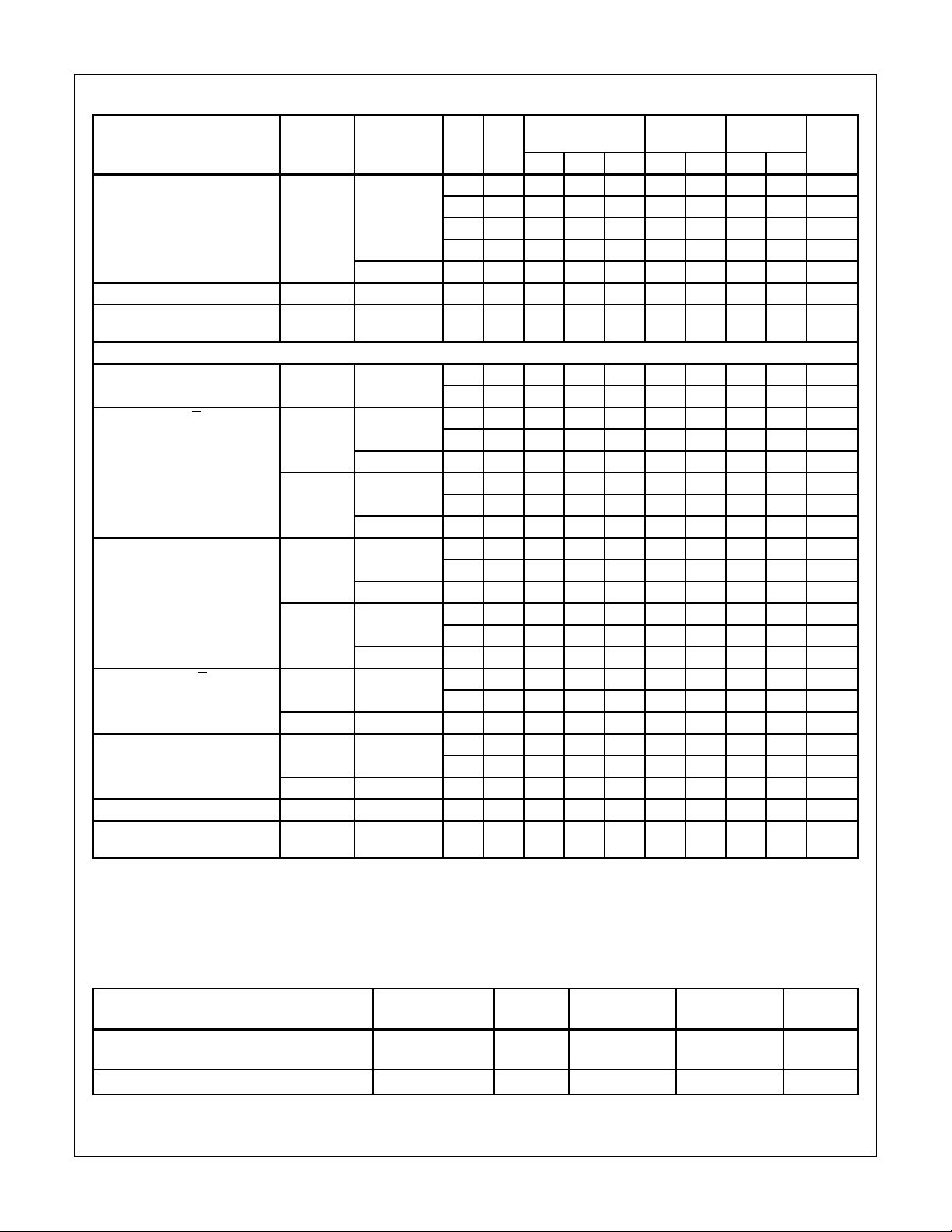
DC Electrical Specifications
CD74HC4316, CD74HCT4316CD74HC4316, CD74HCT4316
PARAMETER SYMBOL
HC TYPES
High Level Input
Voltage
Low Level Input
Voltage
“ON” Resistance
IO = 1mA
Figure 4, 5
Maximum “ON”
Resistance Between
Any Two Channels
Switch Off Leakage
Current
Control Input Leakage
Current
Quiescent Device
Current
IO = 0
R
∆R
V
V
I
ON
I
IZ
I
IL
CC
IH
IL
ON
TEST CONDITIONS 25oC
-40oC TO
85oC
-55oC TO
125oC
UNITSVI(V) VIS(V) VEE (V) VCC (V) MIN TYP MAX MIN MAX MIN MAX
- - - 2 1.5 - - 1.5 - 1.5 - V
4.5 3.15 - - 3.15 - 3.15 - V
6 4.2 - - 4.2 - 4.2 - V
- - - 2 - - 0.5 - 0.5 - 0.5 V
4.5 - - 1.35 - 1.35 - 1.35 V
6 - - 1.8 - 1.8 - 1.8 V
VIH or
V
VCC or
IL
V
EE
0 4.5 - 45 180 - 225 - 270 Ω
0 6 - 35 160 - 200 - 240 Ω
-4.5 4.5 - 30 135 - 170 - 205 Ω
VCC to
V
EE
0 4.5 - 85 320 - 400 - 480 Ω
0 6 - 55 240 - 300 - 360 Ω
-4.5 4.5 - 35 170 - 215 - 255 Ω
- - 0 4.5-10-----Ω
0 6 -8.5-----Ω
-4.5 4.5 - 5 -----Ω
VIH or
V
VCC or
VCC -
IL
V
EE
06--±0.1 - ±1-±1µA
-5 5 - - ±0.1 - ±1-±1µA
-06--±0.1 - ±1-±1µA
GND
VCC or
GND
When
VIS = VEE,
VOS=V
CC
0 6 - - 8 - 80 - 160 µA
-5 5 - - 16 - 160 - 320 µA
HCT TYPES
High Level Input
Voltage
Low Level Input
Voltage
“ON” Resistance
IO = 1mA
Figure 4, 5
Maximum “ON”
Resistance Between
Any Two Channels
Switch Off Leakage
Current
R
∆R
When
VIS=VCC,
VOS =V
EE
V
IH
- - - 4.5 to
2--2-2-V
5.5
V
IL
- - - 4.5 to
- - 0.8 - 0.8 - 0.8 V
5.5
ON
VIH or
V
ON
VCC or
IL
V
EE
VCC to
V
EE
0 4.5 - 45 180 - 225 - 270 Ω
-4.5 4.5 - 30 135 - 170 - 205 Ω
0 4.5 - 85 320 - 400 - 480 Ω
-4.5 4.5 - 35 170 - 215 - 255 Ω
- - 0 4.5-10-----Ω
-4.5 4.5 - 5 -----Ω
I
IZ
VIH or
V
IL
VCC -
V
EE
06--±0.1 - ±1-±1µA
-5 5 - - ±0.1 - ±1-±1µA
4

CD74HC4316, CD74HCT4316CD74HC4316, CD74HCT4316
DC Electrical Specifications (Continued)
TEST CONDITIONS 25
o
C
PARAMETER SYMBOL
Control Input Leakage
Current
Quiescent Device
Current
IO = 0
Additional Quiescent
Device Current Per
I
VCC or
I
- 0 5.5 - - ±0.1 - ±1-±1µA
GND
I
CC
∆I
CC
Any
Voltage
Be-
tween
VCCand
GND
V
CC
-2.1
When
VIS=VEE,
VOS =
0 5.5 - - 8 - 80 - 160 µA
-4.5 5.5 - - 16 - 160 - 320 µA
VCC,
When
VIS=VCC,
VOS=V
EE
- - 4.5 to
- 100 360 - 450 - 490 µA
5.5
Input Pin: 1 Unit Load
NOTE: For dual-supply systems theoretical worst case (VI = 2.4V, VCC = 5.5V) specification is 1.8mA.
HCT Input Loading Table
INPUT UNIT LOADS
All 0.5
NOTE: Unit Load is ∆I
360µA max at 25oC.
Switching Specifications Input t
PARAMETER SYMBOL
HC TYPES
Propagation Delay,
Switch In to Out
Turn “ON” Time E to Out t
Turn “ON” Time nS to Out t
Turn “OFF” Time E to Out t
limit specified in DC Electrical Table, e.g.,
CC
, tf = 6ns
r
TEST
CONDITIONS
t
PLH
PZH
, t
PHL
, t
PZL
CL= 50pF 0 2 - - 60 - 75 - 90 ns
CL= 50pF 0 2 - - 205 - 255 - 310 ns
CL= 15pF - 5 - 17 -----ns
PZH
, t
PZL
CL= 50pF 0 2 - - 175 - 220 - 265 ns
CL= 15pF - 5 - 14 -----ns
PLZ,tPHZ
CL= 50pF 0 2 - - 205 - 255 - 310 ns
CL= 15pF - 5 - 17 -----ns
V
(V)
EE
V
CC
(V)
25oC
0 4.5 - - 12 - 15 - 18 ns
0 6 - - 10 - 13 - 15 ns
-4.5 4.5 - - 8 - 10 - 12 ns
0 4.5 - - 41 - 51 - 62 ns
0 6 - - 35 - 43 - 53 ns
-4.5 4.5 - - 37 - 47 - 56 ns
0 4.5 - - 35 - 44 - 53 ns
0 6 - - 30 - 37 - 45 ns
-4.5 4.5 - - 34 - 43 - 51 ns
0 4.5 - - 41 - 51 - 62 ns
0 6 - - 35 - 43 - 53 ns
-4.5 4.5 - - 37 - 47 - 56 ns
-40oC TO
85oC
-40oC TO
85oC
-55oC TO
125oC
UNITSVI(V) VIS(V) VEE (V) VCC (V) MIN TYP MAX MIN MAX MIN MAX
-55oC TO
125oC
UNITSMIN TYP MAX MIN MAX MIN MAX
5
CD74HC4316, CD74HCT4316CD74HC4316, CD74HCT4316
Switching Specifications Input t
PARAMETER SYMBOL
Turn “OFF” Time nS to Out t
, tf = 6ns (Continued)
r
CONDITIONS
PLZ,tPHZ
CL= 50pF 0 2 - - 175 - 220 - 265 ns
TEST
V
EE
(V)
0 4.5 - - 35 - 44 - 53 ns
0 6 - - 30 - 37 - 45 ns
-4.5 4.5 - - 34 - 43 - 51 ns
CL= 15pF - 5 - 14 -----ns
Input (Control) Capacitance C
Power Dissipation Capacitance
C
I
PD
- ----10-10-10pF
- -5-42-----pF
(Notes 4, 5)
HCT TYPES
Propagation Delay,
Switch In to Switch Out
Turn “ON” Time E to Out t
t
PLH
, t
PZH
PHL
CL= 50pF 0 4.5 - - 12 - 15 - 18 ns
-4.5 4.5 - - 8 - 10 - 12 ns
CL= 50pF 0 4.5 - - 44 - 55 - 66 ns
-4.5 4.5 - - 42 - 53 - 63 ns
CL= 15pF - 5 - 18 -----ns
t
PZL
CL= 50pF 0 4.5 - - 56 - 70 - 85 ns
-4.5 4.5 - - 42 - 53 - 63 ns
CL= 15pF - 5 - 24 -----ns
Turn “ON” Time nS to Out t
PZH
CL= 50pF 0 4.5 - - 40 - 53 - 60 ns
-4.5 4.5 - - 34 - 43 - 51 ns
CL= 15pF - 5 - 17 -----ns
t
PZL
CL= 50pF 0 4.5 - - 50 - 63 - 75 ns
-4.5 4.5 - - 34 - 43 - 51 ns
CL= 15pF - 5 - 18 -----ns
Turn “OFF” Time E to Out t
PLZ
CL= 50pF 0 4.5 - - 50 - 63 - 75 ns
-4.5 4.5 - - 46 - 58 - 69 ns
t
PLZ,tPHZ
Turn “OFF” Time nS to Out t
PHZ
CL= 15pF - 5 - 21 -----ns
CL= 50pF 0 4.5 - - 44 - 55 - 66 ns
-4.5 4.5 - - 40 - 50 - 60 ns
t
PLZ,tPHZ
Input (Control) Capacitance C
Power Dissipation Capacitance
C
I
PD
CL= 15pF - 5 - 18 -----ns
- ----10-10-10pF
- -5-47-----pF
(Notes 4, 5)
NOTES:
4. CPD is used to determine the dynamic power consumption, per package.
5. PD=CPDV
2
fi+ Σ (CL+CS)V
CC
2
fowhere fi= input frequency, fo= output frequency, CL= output load capacitance, CS= switch
CC
capacitance, VCC = supply voltage.
V
(V)
CC
25oC
-40oC TO
85oC
-55oC TO
125oC
UNITSMIN TYP MAX MIN MAX MIN MAX
Analog Channel Specifications T
= 25oC
A
TEST
PARAMETER
Switch Frequency Response Bandwidth at -3dB
CONDITIONS V
Figure 9, Notes 6, 7 4.5 >200 >200 MHz
(V) CD74HC4316 CD74HCT4316 UNITS
CC
Figure 6
Crosstalk Between Any Two Switches Figure 7 Figure 8, Notes 7, 8 4.5 TBE TBE dB
6

CD74HC4316, CD74HCT4316CD74HC4316, CD74HCT4316
Analog Channel Specifications T
= 25oC (Continued)
A
TEST
PARAMETER
Total Harmonic Distortion 1kHz, VIS = 4V
CONDITIONS V
P-P
(V) CD74HC4316 CD74HCT4316 UNITS
CC
4.5 0.078 0.078 %
Figure 10
1kHz, VIS = 8V
P-P
9 0.018 0.018 %
Figure 10
Control to Switch Feedthrough Noise Figure 11 4.5 TBE TBE mV
9 TBE TBE mV
Switch “OFF” Signal Feedthrough Figure 7 Figure 12, Notes 7, 8 4.5 -62 -62 dB
Switch Input Capacitance, C
S
--5 5pF
NOTES:
6. Adjust input level for 0dBm at output, f = 1MHz.
7. VIS is centered at VCC/2.
8. Adjust input for 0dBm at VIS.
Typical Performance Curves
110
100
90
(Ω)
80
ON
70
60
50
40
30
“ON” RESISTANCE, R
20
10
VCC = 4.5V, VEE = 0V
VCC = 6V, VEE = 0V
01 23454.5
INPUT SIGNAL VOLTAGE, V
(V)
IS
FIGURE 4. TYPICAL “ON” RESISTANCE vs INPUT SIGNAL
VOLTAGE
6
60
50
45
(Ω)
ON
40
35
30
25
20
15
“ON” RESISTANCE, R
10
5
0
-4.5 -3.5 -2.5 -1.5 -0.5 1.50.5
VCC = 4.5V, VEE = 4.5V
INPUT SIGNAL VOLTAGE, V
3.5 4.5
2.5
(V)
IS
FIGURE 5. TYPICAL “ON” RESISTANCE vs INPUT SIGNAL
VOLTAGE
0
0
CL = 10pF
V
= 4.5V
CC
RL = 50Ω
= 25oC
T
A
PIN 4 TO 3
FREQUENCY (f), Hz
-1
CL = 10pF
V
= 4.5V
-2
CC
= 50Ω
R
L
T
= 25oC
A
PIN 4 TO 3
-3
CHANNEL ON BANDWIDTH, dB
-4
10K 100K 1M 10M 100M
CL = 10pF
V
= 9V
CC
= 50Ω
R
L
T
= 25oC
A
PIN 4 TO 3
FREQUENCY (f), Hz
-20
-40
-60
CROSSTALK, dB
-80
SWITCH OFF SIGNAL FEEDTHROUGH, dB
-100
10K 100K 1M 10M 100M
FIGURE 6. SWITCH FREQUENCY RESPONSE FIGURE 7. SWITCH-OFF SIGNAL FEEDTHROUGH AND
CROSSTALK vs FREQUENCY
7
CL = 10pF
V
= 9V
CC
RL = 50Ω
= 25oC
T
A
PIN 4 TO 3

CD74HC4316, CD74HCT4316
Analog Test Circuits
V
V
CC
IS
V
0.1µF
V
IS
SWITCH
R
ON
RC
V
OS1
R
VCC/2
V
/2
CC
fIS = 1MHz SINEWAVE
R = 50Ω
C = 10pF
FIGURE 8. CROSSTALK BETWEEN TWO SWITCHES TEST CIRCUIT
V
CC
SINE
10µF
0.1µF
V
IS
SWITCH
ON
V
OS
WAVE
V
IS
50Ω 10pF
dB
V
/2
CC
METER
fIS = 1kHz TO 10kHz
FIGURE 9. FREQUENCY RESPONSE TEST CIRCUIT FIGURE 10. TOTAL HARMONIC DISTORTION TEST CIRCUIT
CC
SWITCH
ON
V
CC
SWITCH
ON
RC
/2
V
CC
VI = V
IH
10kΩ 50pF
/2
V
CC
V
OS2
dB
METER
V
IS
V
OS
DISTORTION
METER
600Ω
/2
E
V
50pF
OS
V
P-P
V
OS
SCOPE
V
CC
600Ω
/2
V
CC
SWITCH
ALTERNATING
ON AND OFF
, tf≤ 6ns
t
r
f
= 1MHz
CONT
50% DUTY
CYCLE
V
CC
FIGURE 11. CONTROL-TO-SWITCH FEEDTHROUGH NOISE
TEST CIRCUIT
V
CC
VC = V
0.1µF
V
IS
SWITCH
ON
R
fIS≥ 1MHz SINEWAVE
R = 50Ω
IL
C = 10pF
V
OS
RC
dB
/2
V
CC
V
/2
CC
METER
FIGURE 12. SWITCH OFF SIGNAL FEEDTHROUGH
8
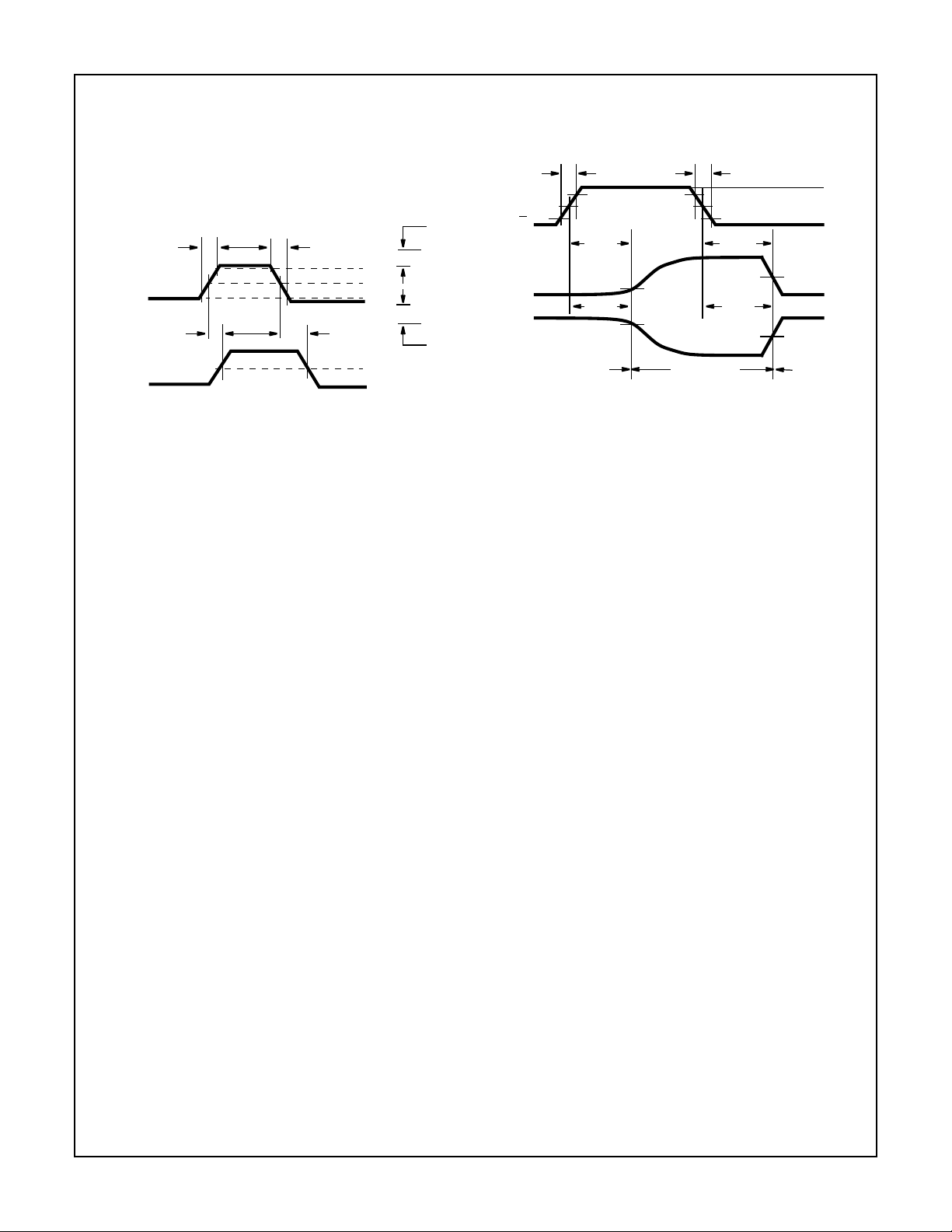
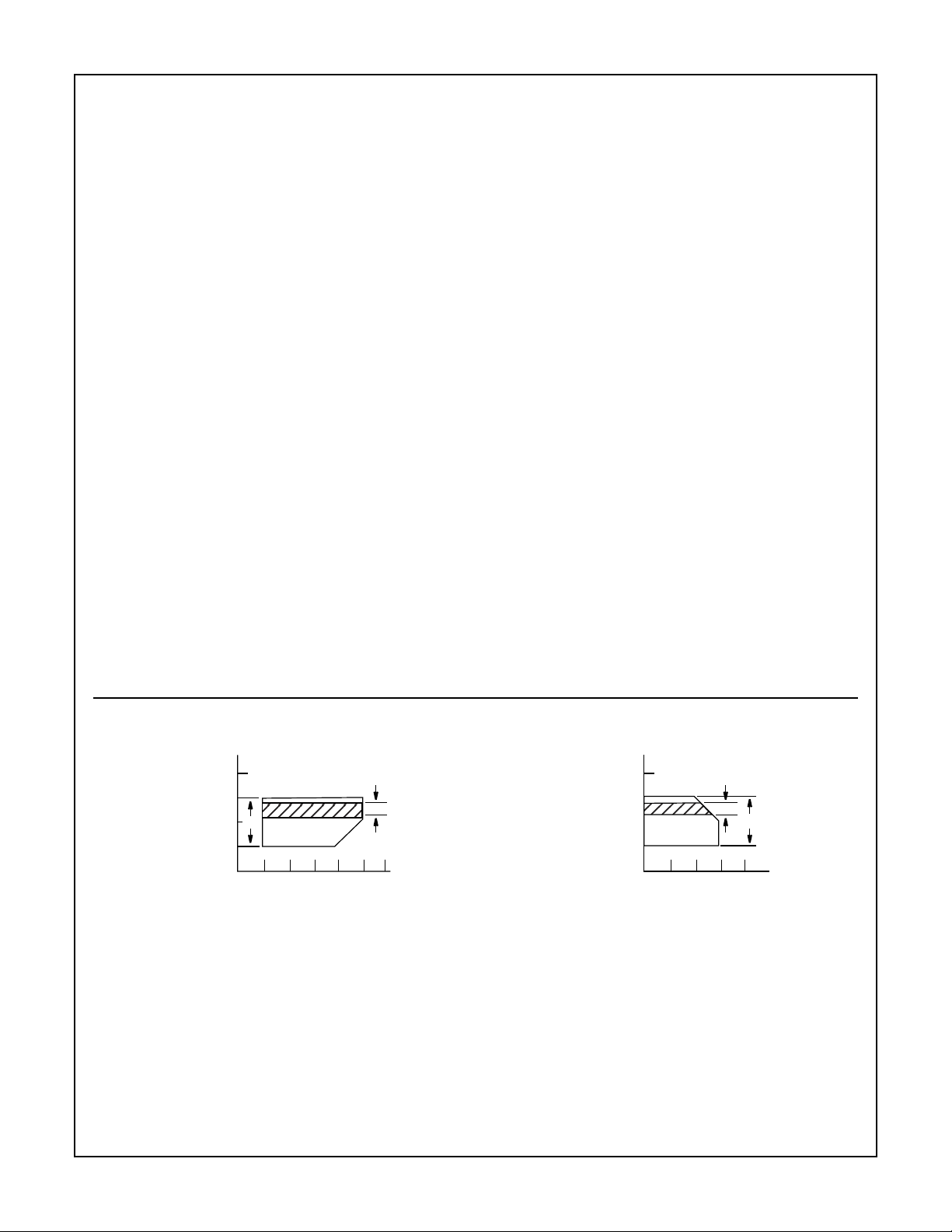
Test Circuits and Waveforms
6ns 6ns
90%
10%
90%
OUTPUTS
DISABLED
SWITCH OFF
tf= 6ns
SWITCH INPUT
t
PLH
SWITCH OUTPUT
tr= 6ns
t
PHL
90%
50%
10%
50%
50%
V
CC
V
EE
E
OUTPUT LOW
TO OFF
OUTPUT HIGH
TO OFF
t
PLZ
t
PHZ
SWITCH
ON
FIGURE 13. SWITCH PROPAGATION DELAY TIMES FIGURE 14. SWITCH TURN-ON AND TURN-OFF
PROPAGATION DELAY TIMES WAVEFORMS
10%
t
PZL
t
PZH
(HC)
V
CC
3V (HCT)
GND
50%
50%
OUTPUTS
ENABLED
SWITCH ON
9

IMPORTANT NOTICE
T exas Instruments and its subsidiaries (TI) reserve the right to make changes to their products or to discontinue
any product or service without notice, and advise customers to obtain the latest version of relevant information
to verify, before placing orders, that information being relied on is current and complete. All products are sold
subject to the terms and conditions of sale supplied at the time of order acknowledgement, including those
pertaining to warranty, patent infringement, and limitation of liability.
TI warrants performance of its semiconductor products to the specifications applicable at the time of sale in
accordance with TI’s standard warranty. Testing and other quality control techniques are utilized to the extent
TI deems necessary to support this warranty . Specific testing of all parameters of each device is not necessarily
performed, except those mandated by government requirements.
CERT AIN APPLICATIONS USING SEMICONDUCTOR PRODUCTS MAY INVOLVE POTENTIAL RISKS OF
DEATH, PERSONAL INJURY, OR SEVERE PROPERTY OR ENVIRONMENTAL DAMAGE (“CRITICAL
APPLICATIONS”). TI SEMICONDUCTOR PRODUCTS ARE NOT DESIGNED, AUTHORIZED, OR
WARRANTED TO BE SUITABLE FOR USE IN LIFE-SUPPORT DEVICES OR SYSTEMS OR OTHER
CRITICAL APPLICA TIONS. INCLUSION OF TI PRODUCTS IN SUCH APPLICATIONS IS UNDERST OOD TO
BE FULLY AT THE CUSTOMER’S RISK.
In order to minimize risks associated with the customer’s applications, adequate design and operating
safeguards must be provided by the customer to minimize inherent or procedural hazards.
TI assumes no liability for applications assistance or customer product design. TI does not warrant or represent
that any license, either express or implied, is granted under any patent right, copyright, mask work right, or other
intellectual property right of TI covering or relating to any combination, machine, or process in which such
semiconductor products or services might be or are used. TI’s publication of information regarding any third
party’s products or services does not constitute TI’s approval, warranty or endorsement thereof.
Copyright 1999, Texas Instruments Incorporated
 Loading...