

OUTPUT STATE
†
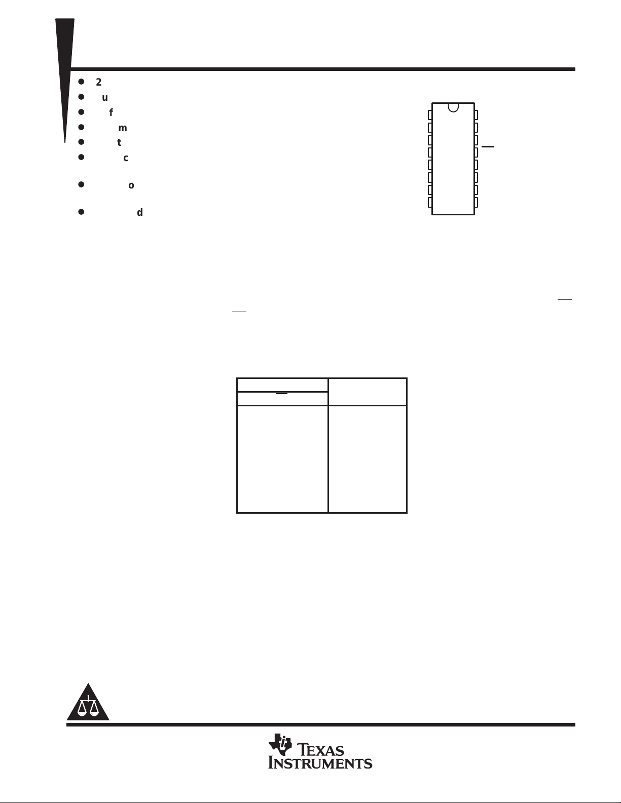
CD54HC4017
DECADE COUNTER/DIVIDER
WITH TEN DECODED OUTPUTS
SGDS011 – MAY 1999
GND
F PACKAGE
(TOP VIEW)
5
1
1
2
0
3
2
4
5
6
6
7
7
3
8
16
15
14
13
12
11
10
V
CC
MR
CP
CE
TC
9
4
9
8
D
2-V to 6-V Operation
D
Fully Static Operation
D
Buffered Inputs
D
Common Reset
D
Positive-Edge Clocking
D
Balanced Propagation Delay and Transition
Times
D
High Noise Immunity: NIL = 30%, NIH = 30%
of VCC at VCC = 5 V
D
Packaged in Ceramic (F) DIP Package and
Also Available in Chip Form (H)
description
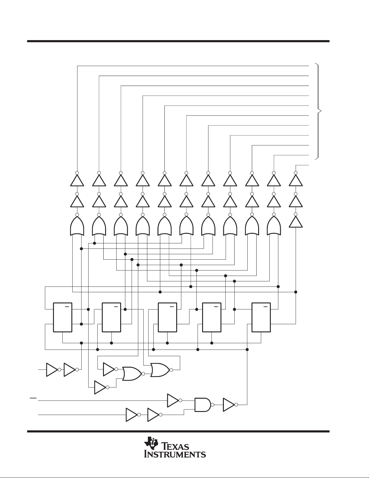
The CD54HC4017 is a high-speed silicon-gate CMOS 5-stage Johnson counter with ten decoded outputs. Each
decoded output normally is low and sequentially goes high on the low-to-high transition of the clock (CP) input.
Each output stays high for one clock period of the ten-clock-period cycle. The terminal count (TC) output
transitions low to high after output ten (9) goes low, and can be used in conjunction with the clock enable (CE)
input to cascade several stages. CE disables counting when in the high state. The master reset (MR) input, when
taken high, sets all the decoded outputs, except 0, to low.
The CD54HC4017 is characterized for operation over the full military temperature range of –55°C to 125°C.
FUNCTION TABLE
INPUTS
CP CE MR
L X L No change
X H L No change
X XH
↑ L L Increments counter
↓ X L No change
X ↑ L No change
H ↓ L Increments counter
†
If n < 5, TC = H; otherwise, TC = L.
0 = H
1–9 = L
Please be aware that an important notice concerning availability, standard warranty, and use in critical applications of
Texas Instruments semiconductor products and disclaimers thereto appears at the end of this data sheet.
PRODUCTION DATA information is current as of publication date.
Products conform to specifications per the terms of Texas Instruments
standard warranty. Production processing does not necessarily include
testing of all parameters.
POST OFFICE BOX 655303 • DALLAS, TEXAS 75265
Copyright 1999, Texas Instruments Incorporated
1
CD54HC4017
DECADE COUNTER/DIVIDER
WITH TEN DECODED OUTPUTS
SGDS011 – MAY 1999
logic diagram (positive logic)
10
11
12
3
0
2
1
4
2
7
3
4
1
5
5
6
6
9
Decoded Decimal Out
7
8
9
TC
2
MR
CE
CP
15
13
14
D
Q
C
Q
R
D
Q
C
Q
R
POST OFFICE BOX 655303 • DALLAS, TEXAS 75265
D
Q
C
Q
R
D
Q
C
Q
R
D
Q
C
Q
R
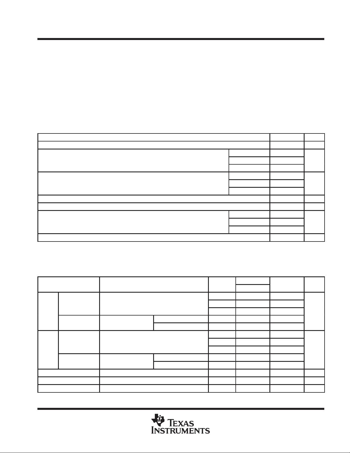
PARAMETER
TEST CONDITIONS
V
MIN
MAX
UNIT
TTL loads
V
V
V
TTL loads
V
V
or V
CD54HC4017
DECADE COUNTER/DIVIDER
WITH TEN DECODED OUTPUTS
SGDS011 – MAY 1999
absolute maximum ratings over operating free-air temperature (unless otherwise noted)
Supply voltage range, V
–0.5 V to 7 V. . . . . . . . . . . . . . . . . . . . . . . . . . . . . . . . . . . . . . . . . . . . . . . . . . . . . . . . . .
CC
†
Input clamp current, IIK (VI < 0 V or VI > VCC) ±20 mA. . . . . . . . . . . . . . . . . . . . . . . . . . . . . . . . . . . . . . . . . . . . . .
Output clamp current, IOK (VO < 0 V or VO > VCC) ±20 mA. . . . . . . . . . . . . . . . . . . . . . . . . . . . . . . . . . . . . . . . . .
Continuous output current, each output pin, IO (VO > –0.5 V or VO < VCC + 0.5 V) ±25 mA. . . . . . . . . . . . . .
VCC or ground current, ICC ±50 mA. . . . . . . . . . . . . . . . . . . . . . . . . . . . . . . . . . . . . . . . . . . . . . . . . . . . . . . . . . . . . .
Storage temperature range, T
†
Stresses beyond those listed under “absolute maximum ratings” may cause permanent damage to the device. These are stress ratings only, and
functional operation of the device at these or any other conditions beyond those indicated under “recommended operating conditions” is not
implied. Exposure to absolute-maximum-rated conditions for extended periods may affect device reliability.
–65°C to 150°C. . . . . . . . . . . . . . . . . . . . . . . . . . . . . . . . . . . . . . . . . . . . . . . . . . .
stg
recommended operating (see Note 1)
MIN MAX UNIT
V
V
V
V
V
t
t
T
NOTE 1: All unused inputs of the device must be held at VCC or GND to ensure proper device operation. Refer to TI application report
Supply voltage 2 6 V
CC
VCC = 2 V 1.5
High-level input voltage
IH
Low-level input voltage
IL
Input voltage 0 V
I
Output voltage 0 V
O
Input transition (rise and fall) time
Operating free-air temperature –55 125 °C
A
of Slow or Floating CMOS Inputs
, literature number SCBA004.
VCC = 4.5 V
VCC = 6 V 4.2
VCC = 2 V 0 0.5
VCC = 4.5 V
VCC = 6 V 0 1.8
VCC = 2 V 0 1000
VCC = 4.5 V
VCC = 6 V 0 400
3.15
0 1.35
CC
CC
0 500
V
V
V
V
ns
Implications
electrical characteristics over recommended operating free-air temperature range (unless
otherwise noted)
TA = 25°C
MIN MAX
4.4 4.4
V
0.1 0.1
V
V
V
I
I
C
OH
OL
I
CC
CMOS loads VI = VIH or VIL, IOH = –0.02 mA
=
or
I
IH
IL
CMOS loads VI = VIH or VIL, IOL = 0.02 mA
=
I
IH
IL
VI = VCC or 0 6 V ±100 ±1000 nA
VI = VCC or 0, IO = 0 6 V 8 160 µA
i
CC
2 V 1.9 1.9
4.5 V
6 V 5.9 5.9
IOH = –4 mA 4.5 V 3.98 3.7
IOH = –5.2 mA 6 V 5.48 5.2
2 V 0.1 0.1
4.5 V
6 V 0.1 0.1
IOL = 4 mA 4.5 V 0.26 0.4
IOL = 5.2 mA 6 V 0.26 0.4
2 V to 6 V 10 10 pF
POST OFFICE BOX 655303 • DALLAS, TEXAS 75265
3

CD54HC4017
PARAMETER
V
MIN
MAX
UNIT
twPulse duration
ns
DECADE COUNTER/DIVIDER
WITH TEN DECODED OUTPUTS
SGDS011 – MAY 1999
timing requirements over recommended operating free-air temperature range (unless otherwise
noted)
TA = 25°C
CC
MIN MAX
2 V 6 4
f
clock
t
su
t
h
t
rem
Maximum clock frequency
Setup time, CE to CP
Hold time, CE to CP
Removal time, MR
CP
MR
4.5 V
6 V 35 23
2 V 80 120
4.5 V 16 24
6 V 14 20
2 V 80 120
4.5 V 16 24
6 V 14 20
2 V 75 110
4.5 V
6 V 13 19
2 V 0 0
4.5 V
6 V 0 0
2 V 5 5
4.5 V
6 V 5 5
30 20
15 22
0 0
5 5
MHz
ns
ns
ns
4
POST OFFICE BOX 655303 • DALLAS, TEXAS 75265

timing requirements
CP
MR
CE
CD54HC4017
DECADE COUNTER/DIVIDER
WITH TEN DECODED OUTPUTS
SGDS011 – MAY 1999
TC
0
1
2
3
4
5
6
7
8
9
1
2
3
4
5
6
7
8
0
1
2
9
POST OFFICE BOX 655303 • DALLAS, TEXAS 75265
5

CD54HC4017
(INPUT)
(OUTPUT)
CC
CP
CE
MR
DECADE COUNTER/DIVIDER
WITH TEN DECODED OUTPUTS
SGDS011 – MAY 1999
switching characteristics, CL = 50 pF, TA = 25°C (see Figures 1 and 2)
PARAMETER
f
max
t
pd
t
pd
t
pd
t
pd
t
pd
t
pd
FROM
TO
Any output
TC
Any output
TC
Any output
TC
V
2 V 6 4
4.5 V 20 20
6 V 35 23
2 V 230 345
4.5 V 46 69
6 V 39 59
2 V 230 345
4.5 V 46 69
6 V 39 59
2 V 250 375
4.5 V 50 75
6 V 43 64
2 V 250 375
4.5 V 50 75
6 V 43 64
2 V 230 345
4.5 V 46 69
6 V 39 59
2 V 230 345
4.5 V 46 69
6 V 39 59
TA = 25°C
MIN MAX MIN MAX
TA = –55°C
TO 125°C
UNIT
MHz
ns
ns
ns
ns
ns
ns
operating characteristics
C
Power dissipation capacitance No load 39 pF
pd
PARAMETER TEST CONDITIONS TYP UNIT
6
POST OFFICE BOX 655303 • DALLAS, TEXAS 75265

From Output
Under Test
(see Note A)
High-Level
Pulse
Low-Level
Pulse
PARAMETER MEASUREMENT INFORMATION
Test
Point
C
L
LOAD CIRCUIT
VOLTAGE WAVEFORMS
PULSE DURATIONS
50% V
50% V
t
CC
w
CC
1 kΩ
50% V
50% V
S1
S2
V
V
CC
0 V
V
CC
0 V
CC
CC
CC
CD54HC4017
DECADE COUNTER/DIVIDER
WITH TEN DECODED OUTPUTS
SGDS011 – MAY 1999
PARAMETER
t
t
en
t
dis
tpd or t
Reference
Input
Data
Input
SETUP AND HOLD AND INPUT RISE AND FALL TIMES
PZH
t
PZL
t
PHZ
t
PLZ
t
t
su
90% 90%
t
r
VOLTAGE WAVEFORMS
S1
Open Closed
Closed Open
Open Closed
Closed Open
Open Open
50% V
t
S2
CC
h
50%50%
V
CC
0 V
V
CC
10%10%
0 V
t
f
Input
In-Phase
Output
Out-of-
Phase
Output
PROPAGATION DELAY AND OUTPUT TRANSITION TIMES
NOTES: A. CL includes probe and test-fixture capacitance.
50% V
CC
t
PLH
90% 90%
t
PHL
50% 50%
10% 10%
VOLTAGE WAVEFORMS
B. Waveform 1 is for an output with internal conditions such that the output is low except when disabled by the output control.
Waveform 2 is for an output with internal conditions such that the output is high except when disabled by the output control.
C. Phase relationships between waveforms were chosen arbitrarily . All input pulses are supplied by generators having the following
characteristics: PRR ≤ 1 MHz, ZO = 50 Ω, tr = 6 ns, tf = 6 ns.
D. The outputs are measured one at a time with one input transition per measurement.
E. t
F. t
G. t
PLZ
PZL
PLH
and t
and t
and t
are the same as t
PHZ
are the same as ten.
PZH
are the same as tpd.
PHL
50% V
CC
t
PHL
50%50%
t
r
t
PLH
t
f
.
dis
Figure 1. Load Circuit and Voltage Waveforms
V
CC
0 V
V
OH
10%10%
V
OL
t
f
V
OH
90%90%
V
OL
t
r
Output
Control
t
PZL
Output
Waveform 1
(See Note B)
t
PZH
Output
Waveform 2
(See Note B)
ENABLE AND DISABLE TIMES FOR 3-STATE OUTPUTS
50% V
CC
≈ V
CC
50%
50%
VOLTAGE WAVEFORMS
50% V
CC
t
PLZ
10%
t
PHZ
90%
V
CC
0 V
≈ V
V
OL
V
OH
≈ 0 V
CC
POST OFFICE BOX 655303 • DALLAS, TEXAS 75265
7

CD54HC4017
DECADE COUNTER/DIVIDER
WITH TEN DECODED OUTPUTS
SGDS011 – MAY 1999
PARAMETER MEASUREMENT INFORMATION
CP
0–9
MR
1–9
0, TC
CP
MR
CE
INPUT LEVEL V
V
S
f
t
V
V
V
1
max
PLH
S
t
PHL
S
t
PLH
S
t
f
t
t
w
t
su
V
S
Input
Level
GND
PHL
Input
Level
GND
Input
Level
GND
Input
Level
GND
Input
Level
GND
t
r
V
S
V
S
V
S
t
rem
V
S
0.5 V
0–9
CC
CE
TC
CP
TC
CE
CE
CP
CC
Input
V
S
t
PHL
V
S
V
S
t
w
t
PLH
V
S
V
S
t
PLH
V
S
V
S
t
w
t
su
t
h
V
S
t
PLH
t
PHL
t
PLH
Level
GND
Input
Level
GND
Input
Level
GND
Input
Level
GND
Input
Level
GND
Figure 2. Voltage Waveforms
8
POST OFFICE BOX 655303 • DALLAS, TEXAS 75265

IMPORTANT NOTICE
T exas Instruments and its subsidiaries (TI) reserve the right to make changes to their products or to discontinue
any product or service without notice, and advise customers to obtain the latest version of relevant information
to verify, before placing orders, that information being relied on is current and complete. All products are sold
subject to the terms and conditions of sale supplied at the time of order acknowledgement, including those
pertaining to warranty, patent infringement, and limitation of liability.
TI warrants performance of its semiconductor products to the specifications applicable at the time of sale in
accordance with TI’s standard warranty. Testing and other quality control techniques are utilized to the extent
TI deems necessary to support this warranty . Specific testing of all parameters of each device is not necessarily
performed, except those mandated by government requirements.
CERTAIN APPLICATIONS USING SEMICONDUCTOR PRODUCTS MAY INVOLVE POTENTIAL RISKS OF
DEATH, PERSONAL INJURY, OR SEVERE PROPERTY OR ENVIRONMENTAL DAMAGE (“CRITICAL
APPLICATIONS”). TI SEMICONDUCTOR PRODUCTS ARE NOT DESIGNED, AUTHORIZED, OR
WARRANTED TO BE SUITABLE FOR USE IN LIFE-SUPPORT DEVICES OR SYSTEMS OR OTHER
CRITICAL APPLICA TIONS. INCLUSION OF TI PRODUCTS IN SUCH APPLICATIONS IS UNDERST OOD TO
BE FULLY AT THE CUSTOMER’S RISK.
In order to minimize risks associated with the customer’s applications, adequate design and operating
safeguards must be provided by the customer to minimize inherent or procedural hazards.
TI assumes no liability for applications assistance or customer product design. TI does not warrant or represent
that any license, either express or implied, is granted under any patent right, copyright, mask work right, or other
intellectual property right of TI covering or relating to any combination, machine, or process in which such
semiconductor products or services might be or are used. TI’s publication of information regarding any third
party’s products or services does not constitute TI’s approval, warranty or endorsement thereof.
Copyright 1999, Texas Instruments Incorporated
 Loading...