

/
j
查询5962-8999001EA供应商
CD54HC297, CD74HC297,
CD74HCT297
[ /Title
(CD74
HC297
,
CD74
HCT29
7)
Subect
(HighSpeed
CMOS
Logic
Digital
PhaseLocked
Data sheet acquired from Harris Semiconductor
SCHS177B
November 1997 - Revised May 2003
Features
• Digital Design Avoids Analog Compensation Errors
• Easily Cascadable for Higher Order Loops
• Useful Frequency Range
- K-Clock . . . . . . . . . . . . . . . . . . . . . . . . . .DC to 55MHz (Typ)
- I/D-Clock . . . . . . . . . . . . . . . . . . . . DC to 35MHz (Typ)
• Dynamically Variable Bandwidth
• Very Narrow Bandwidth Attainable
• Power-On Reset
• Output Capability
- Standard. . . . . . . . . . . . . . . . . . . . XORPD
OUT
, ECPD
- Bus Driver. . . . . . . . . . . . . . . . . . . . . . . . . . . . . I/D
• Fanout (Over Temperature Range)
- Standard Outputs . . . . . . . . . . . . . . . . . . 10 LSTTL Loads
- Bus Driver Outputs . . . . . . . . . . . . . 15 LSTTL Loads
• Balanced Propagation Delay and Transition Times
• Significant Power Reduction Compared to LSTTL
Logic ICs
• ’HC297 Types
- Operation Voltage. . . . . . . . . . . . . . . . . . . . . . . . . . . 2 to 6V
- High Noise ImmunityN
= 30%, NIH= 30% of VCC at 5V
IL
• CD74HCT297 Types
- Operation Voltage. . . . . . . . . . . . . . . . . . . . . . . . 4.5 to 5.5V
- Direct LSTTL Input Logic Compatibility
V
= 0.8V (Max), VIH= 2V (Min)
IL
- CMOS Input Compatibility I
≤ 1µA at VOL, V
I
OH
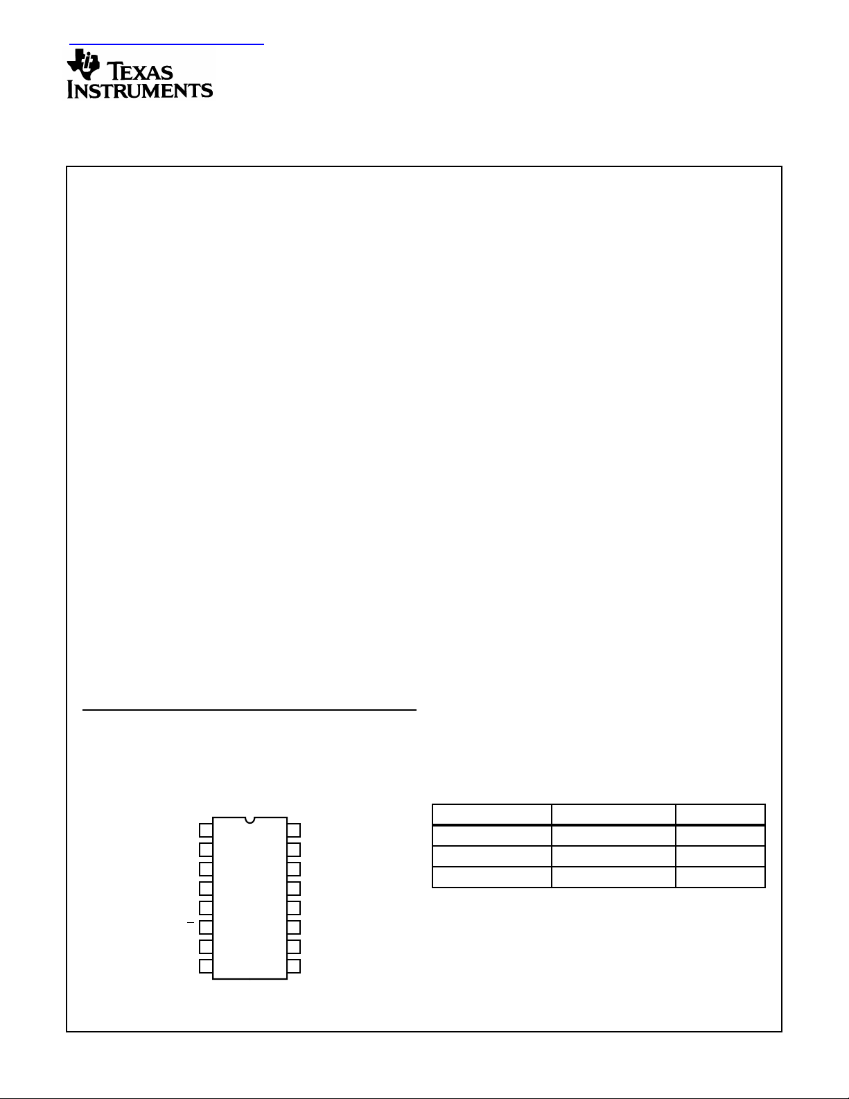
Pinout
CD54HC297
(CERDIP)
CD74HC297, CD74HCT29
(PDIP)
TOP VIEW
16
15
14
13
12
11
10
9
V
CC
C
D
φA
2
ECPD
XORPD
φB
φA
1
OUT
OUT
EN
I/D
CTR
K
I/D
OUT
GND
CP
CP
D/U
1
B
2
A
3
4
5
6
7
8
High-Speed CMOS Logic
Digital Phase-Locked Loop
Description
The ’HC297 and CD74HCT297 are high-speed silicon gate
CMOS devices that are pin-compatible with low power Schottky TTL (LSTTL).
These devices are designed to provide a simple, cost-effective solution to high-accuracy,digital, phase-locked-loop applications. They contain all the necessary circuits, with the
exception of the divide-by-N counter, to build first-order
phase-locked-loops.
Both EXCLUSIVE-OR (XORPD) and edge-controlled phase
detectors (ECPD) are provided for maximum flexibility . The
input signals for the EXCLUSIVE-OR phase detector must
have a 50% duty f actor to obtain the maximum loc k-range .
OUT
Proper partitioning of the loop function, with many of the build-
OUT
ing blocks external to the package, makes it easy for the
designer to incorporate ripple cancellation (see Figure 2) or to
cascade to higher order phase-locked-loops.
The length of the up/down K-counter is digitally programmable
according to the K-counter function table. With A, B, C and D
all LOW,the K-counter is disabled. With A HIGH and B, C and
D LOW,the K-counter is only three stages long, which widens
the bandwidth or capture range and shortens the lock time of
the loop. When A, B, C and D are all programmed HIGH, the
K-counter becomes seventeen stages long, which narrows
the bandwidth or capture range and lengthens the lock time.
Real-time control of loop bandwidth by manipulating the A to
D inputs can maximize the overall performance of the digital
phase-locked-loop .
The ’HC297 and CD74HCT297 can perform the classic first
order phase-locked-loop function without using analog components. The accuracy of the digital phase-locked-loop
(DPLL) is not affected by V
depends solely on accuracies of the K-clock and loop propagation delays.
Ordering Information
PART NUMBER TEMP. RANGE (oC) PACKAGE
CD54HC297F3A -55 to 125 16 Ld CERDIP
CD74HC297E -55 to 125 16 Ld PDIP
CD74HCT297E -55 to 125 16 Ld PDIP
and temperature variations but
CC
CAUTION: These devices are sensitive to electrostatic discharge. Users should follow proper IC Handling Procedures.
Copyright
© 2003, Texas Instruments Incorporated
1
CD54HC297, CD74HC297, CD74HCT297CD54HC297, CD74HC297, CD74HCT297
The phase detector generates an error signal waveform that,
at zero phase error, is a 50% duty factor square wave. At the
limits of linear operation, the phase detector output will be
either HIGH or LOW all of the time depending on the direction
of the phase error (φIN - φOUT). Within these limits the phase
detector output varies linearly with the input phase error
according to the gain K
, which is expressed in terms of
d
phase detector output per cycle or phase error. The phase
detector output can be defined to vary between ±1 according
to the relation:
%HIGH - %LOW
phase detector output =
The output of the phase detector will be K
phase error φ
= φIN - φOUT.
e
--------------------------------------------
100
, where the
dφe
EXCLUSIVE-OR phase detectors (XORPD) and edge-controlled phase detectors (ECPD) are commonly used digital
types. The ECPD is more complex than the XORPD logic
function but can be described generally as a circuit that
changes states on one of the transitions of its inputs. The gain
(K
) for an XORPD is 4 because its output remains HIGH
d
(XORPD
Similarly, K
= 1) for a phase error of one quarter cycle.
OUT
for the ECPD is 2 since its output remains HIGH
d
for a phase error of one half cycle. The type of phase detector
will determine the zero-phase-error point, i.e., the phase separation of the phase detector inputs for a φe defined to be
zero. For the basic DPLL system of Figure 3, φe = 0 when the
phase detector output is a square wave .
The XORPD inputs are one quarter cycle out-of-phase for
zero phase error. For the ECPD, φe = 0 when the inputs are
one half cycle out of phase.
The phase detector output controls the up/down input to the
K-counter. The counter is clocked by input frequency Mf
which is a multiple M of the loop center frequency fc. When
the K-counter recycles up, it generates a carry pulse. Recycling while counting down generates a borrow pulse. If the
carry and the borrow outputs are conceptually combined into
one output that is positive for a carry and negative for a borrow , and if the K-counter is considered as a frequency divider
with the ratio Mf
/K, the output of the K-counter will equal the
c
input frequency multiplied by the division ratio. Thus the output from the K-counter is (K
dφeMfc
)/K.
The carry and borrow pulses go to the increment/decrement
(I/D) circuit which, in the absence of any carry or borrow
pulses has an output that is one half of the input clock (I/D
CP
The input clock is just a multiple, 2N, of the loop center frequency. In response to a carry of borrow pulse, the I/D circuit
will either add or delete a pulse at I/D
the I/D circuit will be Nf
+ (KdφeMfc)/2K.
c
. Thus the output of
OUT
The output of the N-counter (or the output of the phaselocked-loop) is thus: fo = fc + (KdφeMfc)/2KN.
If this result is compared to the equation for a first-order analog phase-locked-loop , the digital equivalent of the gain of the
VCO is just Mf
/2KN or fc/K for M = 2N.
c
Thus, the simple first-order phase-locked-loop with an adjustable K-counter is the equivalent of an analog phase-lockedloop with a programmable VCO gain.
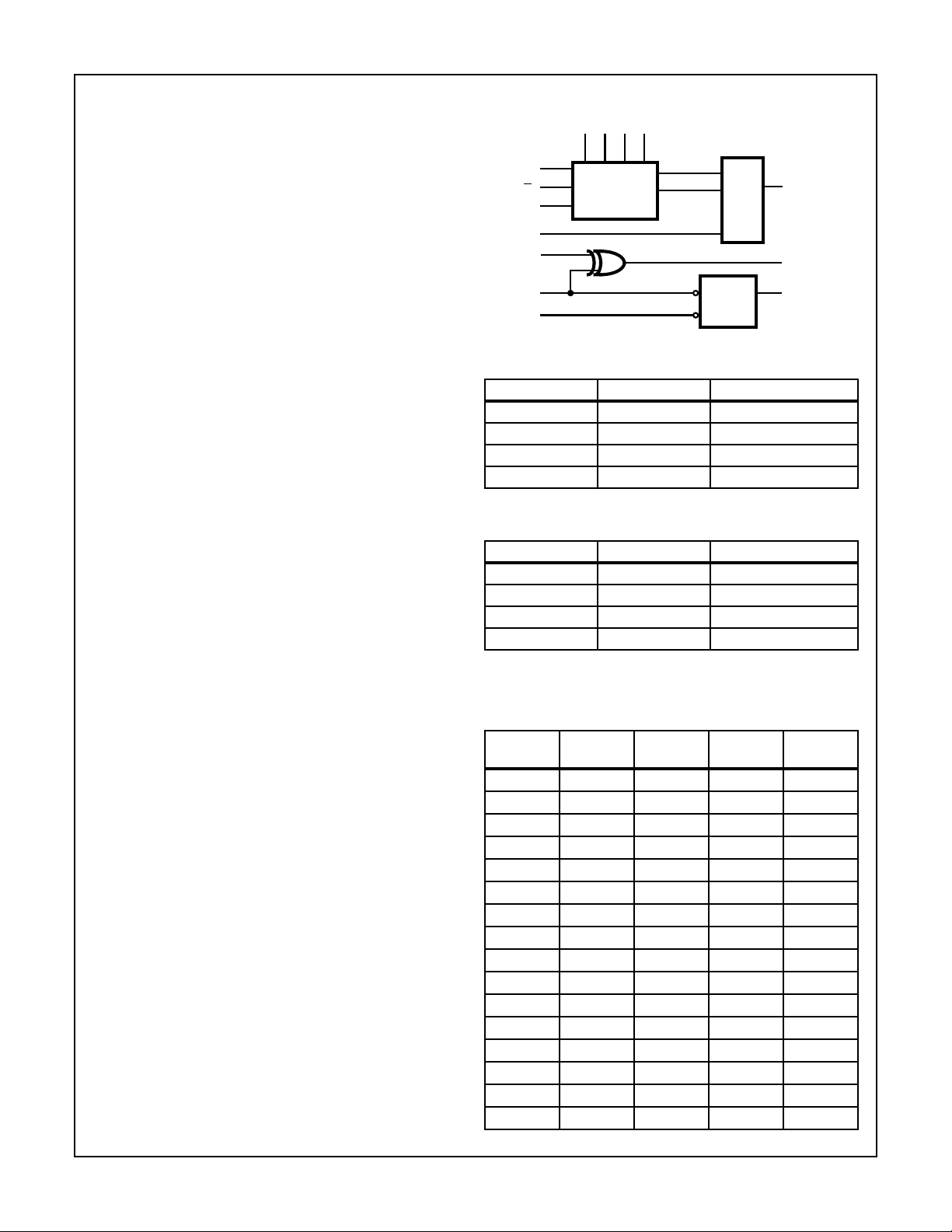
Functional Diagram
DCBA
14 15 1 2
4
K
CP
6
D/U
EN
CTR
I/D
CP
φA
1
φB
φA
2
φA
LL L
LH H
HL H
HH L
φA
H or L
↓
H or L ↑ No Change
↑ H or L No Change
H=Steady-State High Level,L= Steady-StateLowLevel, ↑=LOW
to HIGH φ Transition,↓ = HIGH to LOW φ Transition
c
DCBA
LLLLInhibited
LLLH2
LLHL2
LLHH2
).
LHLL2
LHLH2
LHHL2
LHHH2
HLLL2
HLLH2
HLHL2
HLHH2
HHLL2
HHLH2
HHHL2
HHHH2
MODULO-K
COUNTER
3
5
9
10
13
FUNCTION TABLE
EXCLUSIVE-OR PHASE DETECTOR
1
FUNCTION TABLE
EDGE-CONTROLLED PHASE DETECTOR
2
K-COUNTER FUNCTION TABLE
(DIGITAL CONTROL)
CARRY
BORROW
J
F/F
K
φB XORPD OUT
φB ECPD OUT
↓
H or L L
I/D
CKT
7
11
12
Q
I/D
OUT
XORPD
ECPD
H
MODULO
OUT
OUT
(K)
3
4
5
6
7
8
9
10
11
12
13
14
15
16
17
2
CD54HC297, CD74HC297, CD74HCT297CD54HC297, CD74HC297, CD74HCT297
Absolute Maximum Ratings Thermal Information
DC Supply Voltage, VCC. . . . . . . . . . . . . . . . . . . . . . . . -0.5V to 7V
DC Input Diode Current, I
IK
For VI < -0.5V or VI > VCC + 0.5V. . . . . . . . . . . . . . . . . . . . . .±20mA
DC Output Diode Current, I
OK
For VO < -0.5V or VO > VCC + 0.5V . . . . . . . . . . . . . . . . . . . .±20mA
DC Drain Current, per Output, I
O
For -0.5V < VO < VCC + 0.5V. . . . . . . . . . . . . . . . . . . . . . . . . .±25mA
DC Output Source or Sink Current per Output Pin, I
O
For VO > -0.5V or VO < VCC + 0.5V . . . . . . . . . . . . . . . . . . . .±25mA
DC VCC or Ground Current, ICC . . . . . . . . . . . . . . . . . . . . . . . . .±50mA
Operating Conditions
Temperature Range, TA . . . . . . . . . . . . . . . . . . . . . . -55oC to 125oC
Supply Voltage Range, V
HC Types . . . . . . . . . . . . . . . . . . . . . . . . . . . . . . . . . . . . .2V to 6V
HCT Types . . . . . . . . . . . . . . . . . . . . . . . . . . . . . . . . .4.5V to 5.5V
DC Input or Output Voltage, VI, VO . . . . . . . . . . . . . . . . . 0V to V
Input Rise and Fall Time
2V . . . . . . . . . . . . . . . . . . . . . . . . . . . . . . . . . . . . . . 1000ns (Max)
4.5V. . . . . . . . . . . . . . . . . . . . . . . . . . . . . . . . . . . . . . 500ns (Max)
6V . . . . . . . . . . . . . . . . . . . . . . . . . . . . . . . . . . . . . . . 400ns (Max)
CAUTION: Stresses above those listed in “Absolute Maximum Ratings” may cause permanent damage to the device. This is a stress only rating and operation
of the device at these or any other conditions above those indicated in the operational sections of this specification is not implied.
NOTE:
1. The package thermal impedance is calculated in accordance with JESD 51-7.
CC
Thermal Resistance (Typical, Note 1) θJA (oC/W)
E (PDIP) Package . . . . . . . . . . . . . . . . . . . . . . . . . . 67
Maximum Junction Temperature. . . . . . . . . . . . . . . . . . . . . . . 150oC
Maximum Storage Temperature Range . . . . . . . . . .-65oC to 150oC
Maximum Lead Temperature (Soldering 10s). . . . . . . . . . . . . 300oC
CC
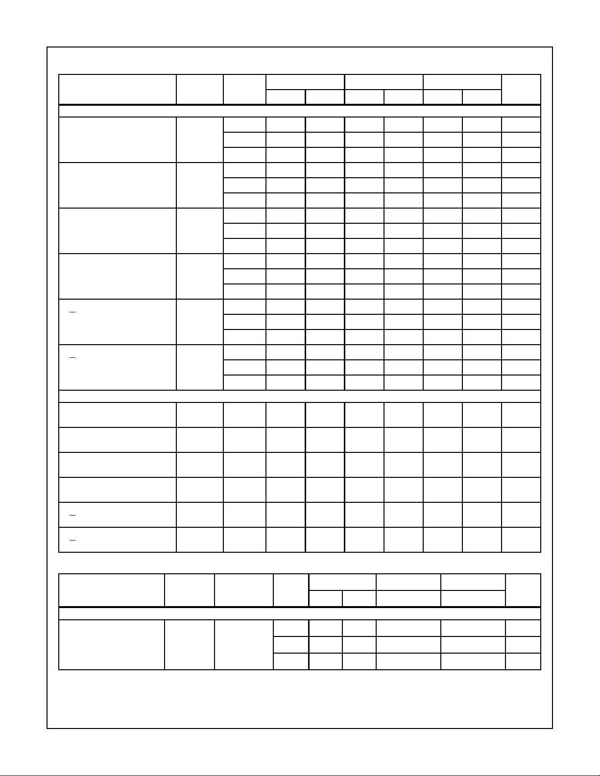
DC Electrical Specifications
PARAMETER SYMBOL
HC TYPES
High Level Input
Voltage
Low Level Input
Voltage
High Level Output
Voltage
CMOS Loads
High Level Output
Voltage
TTL Loads
Low Level Output
Voltage
CMOS Loads
Low Level Output
Voltage
TTL Loads
V
IH
V
IL
V
OH
V
OL
TEST
CONDITIONS
25oC -40oC TO 85oC -55oC TO 125oC
VCC (V)
- - 2 1.5 - - 1.5 - 1.5 - V
4.5 3.15 - - 3.15 - 3.15 - V
6 4.2 - - 4.2 - 4.2 - V
- - 2 - - 0.5 - 0.5 - 0.5 V
4.5 - - 1.35 - 1.35 - 1.35 V
6 - - 1.8 - 1.8 - 1.8 V
VIH or
V
-0.02 2 1.9 - - 1.9 - 1.9 - V
IL
-0.02 4.5 4.4 - - 4.4 - 4.4 - V
-0.02 6 5.9 - - 5.9 - 5.9 - V
-6
4.5 3.98 - - 3.84 - 3.7 - V
(Note 2)
-7.8
6 5.48 - - 5.34 - 5.2 - V
(Note 2)
VIH or
V
0.02 2 - - 0.1 - 0.1 - 0.1 V
IL
0.02 4.5 - - 0.1 - 0.1 - 0.1 V
0.02 6 - - 0.1 - 0.1 - 0.1 V
4
4.5 - - 0.26 - 0.33 - 0.4 V
(Note 2)
5.2
6 - - 0.26 - 0.33 - 0.4 V
(Note 2)
UNITSVI(V) IO(mA) MIN TYP MAX MIN MAX MIN MAX
3
CD54HC297, CD74HC297, CD74HCT297CD54HC297, CD74HC297, CD74HCT297
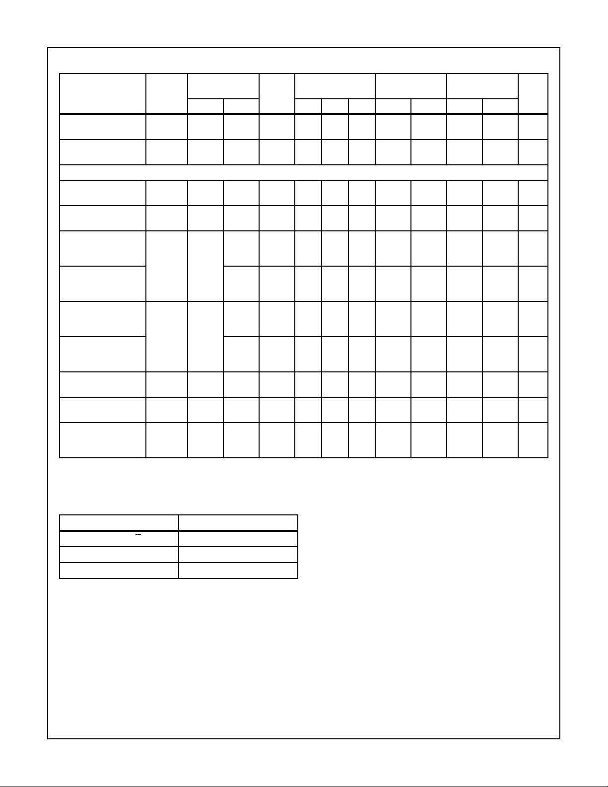
DC Electrical Specifications (Continued)
TEST
CONDITIONS
PARAMETER SYMBOL
Input Leakage
Current
Quiescent Device
Current
I
I
CC
VCC or
I
GND
VCC or
GND
VCC (V)
-6--±0.1 - ±1-±1 µA
0 6 - - 8 - 80 - 160 µA
HCT TYPES
High Level Input
Voltage
Low Level Input
Voltage
High Level Output
Voltage
V
IH
- - 4.5 to
5.5
V
IL
- - 4.5 to
5.5
V
OH
VIH or
V
IL
-0.02 4.5 4.4 - - 4.4 - 4.4 - V
CMOS Loads
High Level Output
-4 4.5 3.98 - - 3.84 - 3.7 - V
Voltage
TTL Loads
Low Level Output
Voltage
V
OL
VIH or
V
IL
0.02 4.5 - - 0.1 - 0.1 - 0.1 V
CMOS Loads
Low Level Output
4 4.5 - - 0.26 - 0.33 - 0.4 V
Voltage
TTL Loads
Input Leakage
Current
Quiescent Device
Current
Additional Quiescent
Device Current Per
I
I
I
CC
∆I
CC
(Note 2)
VCC to
GND
VCC or
GND
V
CC
-2.1
0 5.5 - - ±0.1 - ±1-±1 µA
0 5.5 - - 8 - 80 - 160 µA
- 4.5 to
5.5
Input Pin: 1 Unit Load
NOTE:
2. For dual-supply systems theoretical worst case (VI = 2.4V, VCC = 5.5V) specification is 1.8mA.
25oC -40oC TO 85oC -55oC TO 125oC
2-- 2 - 2 - V
- - 0.8 - 0.8 - 0.8 V
- 100 360 - 450 - 490 µA
UNITSVI(V) IO(mA) MIN TYP MAX MIN MAX MIN MAX
HCT Input Loading Table
INPUT UNIT LOADS
EN
, D/U 0.3
CTR
A, B, C, D, KCP, φA
2
I/DCP, φA1, φB 1.5
NOTE: Unit Load is ∆ICClimit specified in DC Electrical
Specifications table, e.g., 360µA max at 25oC.
0.6
4
CD54HC297, CD74HC297, CD74HCT297CD54HC297, CD74HC297, CD74HCT297
Prerequisite For Switching Function
PARAMETER SYMBOL VCC (V)
HC TYPES
Maximum Clock Frequency
K
CP
Maximum Clock Frequency
I/D
CP
Clock Pulse Width
K
CP
Clock Pulse Width
I/D
CP
Set-up Time
D/U, EN
CTR
to K
CP
Hold Time
D/U, EN
CTR
to K
CP
HCT TYPES
Maximum Clock Frequency
K
CP
Maximum Clock Frequency
I/D
CP
Clock Pulse Width
K
CP
Clock Pulse Width
I/D
CP
Set-up Time
D/U, EN
CTR
to K
CP
Hold Time
D/U, EN
CTR
to K
CP
f
MAX
f
MAX
t
t
f
MAX
f
MAX
t
t
W
SU
t
t
t
SU
t
w
H
w
w
H
25oC -40oC TO 85oC -55oC TO 125oC
UNITSMIN MAX MIN MAX MIN MAX
26-5-4-MHz
4.5 30 - 24 - 20 - MHz
6 35 - 28 - 24 - MHz
24-3-2-MHz
4.5 20 - 16 - 13 - MHz
6 24 - 19 - 15 - MHz
2 80 - 100 - 120 - ns
4.5 16 - 20 - 24 - ns
614-17-20-ns
2 125 - 155 - 190 - ns
4.5 25 - 31 - 38 - ns
621-26-32-ns
2 100 - 125 - 150 - ns
4.5 20 - 25 - 30 - ns
617-21-26-ns
20-0-0-ns
4.50-0-0-ns
60-0-0-ns
4.5 30 - 24 - 20 - MHz
4.5 20 - 16 - 13 - MHz
4.5 16 - 20 - 24 - ns
4.5 25 - 31 - 38 - ns
4.5 20 - 25 - 30 - ns
4.50-0-0-ns
Switching Specifications Input t
PARAMETER SYMBOL
HC TYPES
Propagation Delay,
I/DCP to I/D
OUT
t
PLH
, t
, tf = 6ns
r
TEST
CONDITIONS VCC (V)
PHLCL
= 50pF 2 - 175 220 265 ns
25oC -40oC TO 85oC -55oC TO 125oC
UNITSTYP MAX MAX MAX
4.5 - 35 44 53 ns
6 - 30 34 43 ns
5

CD54HC297, CD74HC297, CD74HCT297CD54HC297, CD74HC297, CD74HCT297
Switching Specifications Input t
PARAMETER SYMBOL
Propagation Delay,
φA1, φB to XORPD
OUT
Propagation Delay,
φB, φA2 to ECPD
OUT
Output Transition Time
XORPD
OUT
ECPD
OUT
Output Transition Time
I/D
OUT
Input Capacitance C
HCT TYPES
Propagation Delay,
I/DCP to I/D
OUT
Propagation Delay,
φA1, φB to XORPD
OUT
Propagation Delay,
φB, φA2 to ECPD
OUT
Output Transition Time
XORPD
OUT
Output Transition Time
ECPD
OUT
Input Capacitance C
t
PLH
t
PHL
t
PLH
t
PLH
t
PHL
t
TLH
t
TLH
t
TLH
t
TLH
, t
, t
I
, t
, t
, t
I
, tf = 6ns (Continued)
r
TEST
25oC -40oC TO 85oC -55oC TO 125oC
CONDITIONS VCC (V)
PHLCL
= 50pF 2 - 150 190 225 ns
4.5 - 30 38 45 ns
6 - 26 33 38 ns
PHLCL
= 50pF 2 - 200 250 300 ns
4.5 - 40 50 60 ns
6 - 34 43 51 ns
CL= 50pF 2 - 75 95 110 ns
4.5 - 15 19 22 ns
6 - 13 16 19 ns
CL= 50pF 2 - 60 75 90 ns
4.5 - 12 15 18 ns
6 - 10 13 15 ns
---1010 10pF
PHLCL
PHLCL
PHLCL
= 50pF 4.5 - 35 44 53 ns
= 50pF 4.5 - 30 38 45 ns
= 50pF 4.5 - 40 50 60 ns
CL= 50pF 4.5 - 15 19 22 ns
CL= 50pF 4.5 - 12 15 18 ns
---1010 10pF
UNITSTYP MAX MAX MAX
6

Logic Diagram
2
A
1
B
15
C
14
D
4
K
CP
6
D/U
3
EN
CTR
POWER ON RESET
1 = 1 1
CD54HC297, CD74HC297, CD74HCT297CD54HC297, CD74HC297, CD74HCT297
MODULO-K COUNTER
1
D
CP
D
CP
FF
FF
2
4
0
8
R
D
T
Q
Q
FF
Q
T
FF
Q
R
D
CONTROL CIRCUIT
R
D
T
FF
Q
T
FF
Q
R
D
1413121110987654321
R
D
D
FF14
T
M
M
FF14
T
D
R
D
TO MODE CONTROLS 12-2
(11 STAGES NOT SHOWN)
R
D
D
Q
T
Q
Q
M
M
T
D
FF13
FF13
R
D
Q
R
D
D
Q
T
FF1
R
D
Q
T
FF
M
Q
M
FF1
T
D
R
D
Q
FF
T
R
D
I/D
φA
CP
φB
BORROW
CARRY
5
INCREMENT/DECREMENT CIRCUIT
7
I/D
OUT
D
CP
Q
FF
Q
D
CP
FF
CP
D
Q
FF
Q
Q
D
CP
FF
Q
Q
J
FF
CP
KQ
D
CP
FF
Q
Q
D
CP
Q
FF
Q
D
CP
FF
Q
D
CP
FF
Q
9
1
10
EXCLUSIVE-OR PHASE DETECTOR
11
XORPD
OUT
φA
EDGE-CONTROLLED PHASE DETECTOR
S
D
Q
FF
Q
R
13
2
D
S
FF
R
D
Q
Q
D
12
ECPD
OUT
7

CD54HC297, CD74HC297, CD74HCT297CD54HC297, CD74HC297, CD74HCT297
CARRY
BORROW
I/D
OUT
I/D CIRCUIT
I/D
CP
2Nf
C
f
φ
Mf
OUT
OUT
f
φ
K
EN
CTR
XORPD
φA
CP
D/U
DIVIDE-BY-K
COUNTER
OUT
1
C
φB
ECPD
OUT
JJ
ECPD
φA
IN
IN
2
K
FF
DIVIDE-BY-N
COUNTER
FIGURE 1. DPLL USING BOTH PHASE DETECTORS IN A RIPPLE-CANCELLATION SCHEME
Mf
f
OUT
K
XORPD
CP
D/U
OUT
φA
φB
DIVIDE-BY-K
COUNTER
1
C
φ
IN
CARRY
BORROW
I/D CIRCUIT
I/D
CP
2Nf
C
f
OUT
φ
OUT
FIGURE 2. DPLL USING EXCLUSIVE-OR PHASE DETECTION
CARRY PULSE
(INTERNAL SIGNAL)
BORROW PULSE
(INTERNAL SIGNAL)
I/D
INPUT
CP
OUTPUT
I/D
OUT
FIGURE 3. TIMING DIAGRAM: I/D
DIVIDE-BY-N
COUNTER
I/D
OUT
IN-LOCK CONDITION
OUT
8

CD54HC297, CD74HC297, CD74HCT297
øB INPUT
øA
INPUT
2
ECPD
OUT
OUTPUT
FIGURE 4. TIMING DIAGRAM: EDGE CONTROLLED PHASE COMPARATOR WAVEFORMS
øB INPUT
INPUT
øA
1
XORPD
OUT
OUTPUT
FIGURE 5. TIMING DIAGRAM: EXCLUSIVE OR PHASE DETECTOR WAVEFORMS
I/f
MAX
t
W
I/D
I/D
CP
t
PLH
OUT
t
TLH
V
S
t
PHL
V
S
t
THL
FIGURE 6. WAVEFORMS SHOWINGTHE CLOCK (I/DCP) TO OUTPUT (I/D
) PROPAGATION DELAYS, CLOCK PULSE WIDTH,
OUT
OUTPUT TRANSITION TIMES AND MAXIMUM CLOCK PULSE FREQUENCY
V
øB INPUT
øA1 INPUT
XORPD
OUT
OUTPUT
t
PLH
t
PLH
V
S
V
S
S
t
TLH
t
PLH
t
THL
FIGURE 7. WAVEFORMS SHOWING THE PHASE INPUT (øB, øA1) TO OUTPUT (XORPD
OUTPUT TRANSITION TIMES
t
PHL
) PROPAGATION DELAYS AND
OUT
9

CD54HC297, CD74HC297, CD74HCT297
OUT
t
PHL
V
S
V
S
V
S
t
PLH
t
THL
t
TLH
) PROPAGATION DELAYSANDOUTPUT
OUT
øB INPUT
øA2 INPUT
ECPD
OUTPUT
FIGURE 8. WAVEFORMSSHOWING THE PHASE INPUT (øB, øA2) TOOUTPUT(ECPD
TRANSITION TIMES
D/U, EN
CTR
INPUT
KCP INPUT
t
H
V
S
t
SU
t
SU
V
S
t
W
1/f
MAX
t
H
NOTE: The shaded areas indicate when the input is permitted to change for predictable output performance.
FIGURE 9. WAVEFORMS SHOWINGTHE CLOCK (KCP) PULSE WIDTH AND MAXIMUM CLOCK PULSE FREQUENCY, AND THE
INPUT (D/U, EN
) TO CLOCK (KCP) SETUP AND HOLD TIMES
CTR
10

PACKAGE OPTION ADDENDUM
www.ti.com
26-Sep-2005
PACKAGING INFORMATION
Orderable Device Status
(1)
Package
Type
Package
Drawing
Pins Package
Qty
Eco Plan
5962-8999001EA ACTIVE CDIP J 16 1 TBD Call TI Level-NC-NC-NC
CD54HC297F3A ACTIVE CDIP J 16 1 TBD Call TI Level-NC-NC-NC
CD74HC297E ACTIVE PDIP N 16 25 Pb-Free
CD74HC297EE4 ACTIVE PDIP N 16 25 Pb-Free
CD74HCT297E ACTIVE PDIP N 16 25 Pb-Free
CD74HCT297EE4 ACTIVE PDIP N 16 25 Pb-Free
(1)
The marketing status values are defined as follows:
ACTIVE: Product device recommended for new designs.
LIFEBUY: TI has announced that the device will be discontinued, and a lifetime-buy period is in effect.
NRND: Not recommended for new designs. Device is in production to support existing customers, but TI does not recommend using this part in
a new design.
PREVIEW: Device has been announced but is not in production. Samples may or may not be available.
OBSOLETE: TI has discontinued the production of the device.
(2)
Eco Plan - The planned eco-friendly classification: Pb-Free (RoHS) or Green (RoHS & no Sb/Br) - please check
http://www.ti.com/productcontent for the latest availability information and additional product content details.
TBD: The Pb-Free/Green conversion plan has not been defined.
Pb-Free (RoHS): TI's terms "Lead-Free" or "Pb-Free" mean semiconductor products that are compatible with the current RoHS requirements
for all 6 substances, including the requirement that lead not exceed 0.1% by weight in homogeneous materials. Where designed to be soldered
at high temperatures, TI Pb-Free products are suitable for use in specified lead-free processes.
Green (RoHS & no Sb/Br): TI defines "Green" to mean Pb-Free (RoHS compatible), and free of Bromine (Br) and Antimony (Sb) based flame
retardants (Br or Sb do not exceed 0.1% by weight in homogeneous material)
(RoHS)
(RoHS)
(RoHS)
(RoHS)
(2)
Lead/Ball Finish MSL Peak Temp
CU NIPDAU Level-NC-NC-NC
CU NIPDAU Level-NC-NC-NC
CU NIPDAU Level-NC-NC-NC
CU NIPDAU Level-NC-NC-NC
(3)
(3)
MSL, Peak Temp. -- The Moisture Sensitivity Level rating according to the JEDEC industry standard classifications, and peak solder
temperature.
Important Information and Disclaimer:The information provided on this page represents TI's knowledge and belief as of the date that it is
provided. TI bases its knowledge and belief on information provided by third parties, and makes no representation or warranty as to the
accuracy of such information. Efforts are underway to better integrate information from third parties. TI has taken and continues to take
reasonable steps to provide representative and accurate information but may not have conducted destructive testing or chemical analysis on
incoming materials and chemicals. TI and TI suppliers consider certain information to be proprietary, and thus CAS numbers and other limited
information may not be available for release.
In no event shall TI's liability arising out of such information exceed the total purchase price of the TI part(s) at issue in this document sold by TI
to Customer on an annual basis.
Addendum-Page 1


IMPORTANT NOTICE
Texas Instruments Incorporated and its subsidiaries (TI) reserve the right to make corrections, modifications,
enhancements, improvements, and other changes to its products and services at any time and to discontinue
any product or service without notice. Customers should obtain the latest relevant information before placing
orders and should verify that such information is current and complete. All products are sold subject to TI’s terms
and conditions of sale supplied at the time of order acknowledgment.
TI warrants performance of its hardware products to the specifications applicable at the time of sale in
accordance with TI’s standard warranty. Testing and other quality control techniques are used to the extent TI
deems necessary to support this warranty . Except where mandated by government requirements, testing of all
parameters of each product is not necessarily performed.
TI assumes no liability for applications assistance or customer product design. Customers are responsible for
their products and applications using TI components. To minimize the risks associated with customer products
and applications, customers should provide adequate design and operating safeguards.
TI does not warrant or represent that any license, either express or implied, is granted under any TI patent right,
copyright, mask work right, or other TI intellectual property right relating to any combination, machine, or process
in which TI products or services are used. Information published by TI regarding third-party products or services
does not constitute a license from TI to use such products or services or a warranty or endorsement thereof.
Use of such information may require a license from a third party under the patents or other intellectual property
of the third party, or a license from TI under the patents or other intellectual property of TI.
Reproduction of information in TI data books or data sheets is permissible only if reproduction is without
alteration and is accompanied by all associated warranties, conditions, limitations, and notices. Reproduction
of this information with alteration is an unfair and deceptive business practice. TI is not responsible or liable for
such altered documentation.
Resale of TI products or services with statements different from or beyond the parameters stated by TI for that
product or service voids all express and any implied warranties for the associated TI product or service and
is an unfair and deceptive business practice. TI is not responsible or liable for any such statements.
Following are URLs where you can obtain information on other Texas Instruments products and application
solutions:
Products Applications
Amplifiers amplifier.ti.com Audio www.ti.com/audio
Data Converters dataconverter.ti.com Automotive www.ti.com/automotive
DSP dsp.ti.com Broadband www.ti.com/broadband
Interface interface.ti.com Digital Control www.ti.com/digitalcontrol
Logic logic.ti.com Military www.ti.com/military
Power Mgmt power.ti.com Optical Networking www.ti.com/opticalnetwork
Microcontrollers microcontroller.ti.com Security www.ti.com/security
Telephony www.ti.com/telephony
Video & Imaging www.ti.com/video
Wireless www.ti.com/wireless
Mailing Address: Texas Instruments
Post Office Box 655303 Dallas, Texas 75265
Copyright 2005, Texas Instruments Incorporated
 Loading...