

[
(
H
,
C
H
3
/
j
(
S
C
L
4
B
F
A
查询CD54HC283F3A供应商
Data sheet acquired from Harris Semiconductor
SCHS176D
November 1997 - Revised October 2003
CD54HC283, CD74HC283,
CD54HCT283, CD74HCT283
High-Speed CMOS Logic
4-Bit Binary Full Adder with Fast Carry
/Title
CD74
C283
D74
CT28
)
Subect
High
peed
MOS
ogic
-Bit
inary
ull
dder
Features
• Adds Two Binary Numbers
• Full Internal Lookahead
• Fast Ripple Carry for Economical Expansion
• Operates with Both Positive and Negative Logic
• Fanout (Over Temperature Range)
- Standard Outputs. . . . . . . . . . . . . . . 10 LSTTL Loads
- Bus Driver Outputs . . . . . . . . . . . . . 15 LSTTL Loads
• Wide Operating Temperature Range . . . -55
• Balanced Propagation Delay and Transition Times
• Significant Power Reduction Compared to LSTTL
Logic ICs
• HC Types
- 2V to 6V Operation
- High Noise Immunity: N
= 30%, NIH = 30% of V
IL
at VCC = 5V
• HCT Types
- 4.5V to 5.5V Operation
- Direct LSTTL Input Logic Compatibility,
V
= 0.8V (Max), VIH = 2V (Min)
IL
- CMOS Input Compatibility, I
≤ 1µA at VOL, V
l
o
C to 125oC
OH
Description
The ’HC283 and ’HCT283 binary full adders add two 4-bit
binary numbers and generate a carry-out bit if the sum
exceeds 15.
Because of the symmetry of the add function, this device
can be used with either all active-high operands (positive
logic) or with all active-low operands (negative logic). When
using positive logicthe carry-in input must be tied low if there
is no carry-in.
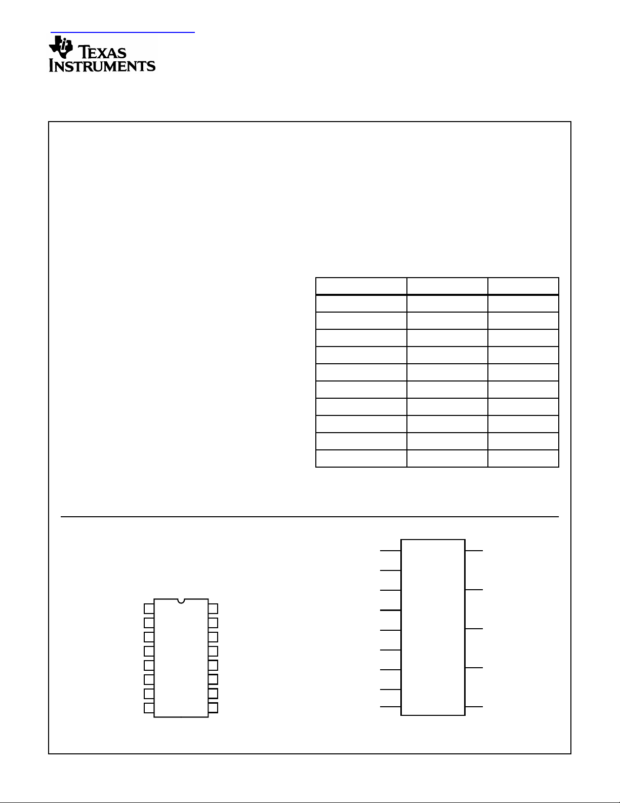
Ordering Information
PART NUMBER TEMP. RANGE (oC) PACKAGE
CD54HC283F3A -55 to 125 16 Ld CERDIP
CD54HCT283F3A -55 to 125 16 Ld CERDIP
CD74HC283E -55 to 125 16 Ld PDIP
CC
CD74HC283M -55 to 125 16 Ld SOIC
CD74HC283MT -55 to 125 16 Ld SOIC
CD74HC283M96 -55 to 125 16 Ld SOIC
CD74HCT283E -55 to 125 16 Ld PDIP
CD74HCT283M -55 to 125 16 Ld SOIC
CD74HCT283MT -55 to 125 16 Ld SOIC
CD74HCT283M96 -55 to 125 16 Ld SOIC
NOTE: When ordering, use the entire part number. The suffix 96
denotes tape and reel. The suffix T denotes a small-quantity reel of
250.
Pinout
CD54HC283, CD54HCT283
(CERDIP)
CD74HC283, CD74HCT283
(PDIP, SOIC)
TOP VIEW
16
1
S1
2
B1
3
A1
4
S0
5
A0
6
B0
7
C
IN
8
GND
CAUTION: These devices are sensitive to electrostatic discharge. Users should follow proper IC Handling Procedures.
Copyright
© 2003, Texas Instruments Incorporated
V
CC
15
B2
14
A2
13
S2
12
A3
B3
11
10
S3
9
C
OUT
Functional Diagram
5
A0
6
B0
3
A1
2
B1
14
A2
15
B2
12
A3
11
B3
7
C
IN
1
4
S0
1
S1
13
S2
10
S3
9
C
GND = 8
= 16
V
CC
OUT
CD54HC283, CD74HC283, CD54HCT283, CD74HCT283
Absolute Maximum Ratings Thermal Information
DC Supply Voltage, VCC. . . . . . . . . . . . . . . . . . . . . . . . -0.5V to 7V
DC Input Diode Current, I
IK
For VI < -0.5V or VI > VCC + 0.5V. . . . . . . . . . . . . . . . . . . . . .±20mA
DC Output Diode Current, I
OK
For VO < -0.5V or VO > VCC + 0.5V . . . . . . . . . . . . . . . . . . . .±20mA
DC Drain Current, per Output, I
O
For -0.5V < VO < VCC + 0.5V. . . . . . . . . . . . . . . . . . . . . . . . . .±25mA
DC Output Source or Sink Current per Output Pin, I
O
For VO > -0.5V or VO < VCC + 0.5V . . . . . . . . . . . . . . . . . . . .±25mA
DC VCC or Ground Current, ICC . . . . . . . . . . . . . . . . . . . . . . . . .±50mA
Operating Conditions
Temperature Range, TA . . . . . . . . . . . . . . . . . . . . . . -55oC to 125oC
Supply Voltage Range, V
HC Types . . . . . . . . . . . . . . . . . . . . . . . . . . . . . . . . . . . . .2V to 6V
DC Input or Output Voltage, VI, VO . . . . . . . . . . . . . . . . . 0V to V
Input Rise and Fall Time
2V . . . . . . . . . . . . . . . . . . . . . . . . . . . . . . . . . . . . . . 1000ns (Max)
4.5V. . . . . . . . . . . . . . . . . . . . . . . . . . . . . . . . . . . . . . 500ns (Max)
6V . . . . . . . . . . . . . . . . . . . . . . . . . . . . . . . . . . . . . . . 400ns (Max)
CAUTION: Stresses above those listed in “Absolute Maximum Ratings” may cause permanent damage to the device. This is a stress only rating and operation
of the device at these or any other conditions above those indicated in the operational sections of this specification is not implied.
NOTE:
1. The package thermal impedance is calculated in accordance with JESD 51-7.
CC
Thermal Resistance (Typical, Note 1) θJA (oC/W)
E (PDIP) Package . . . . . . . . . . . . . . . . . . . . . . . . . . 67
M (SOIC) Package. . . . . . . . . . . . . . . . . . . . . . . . . . 73
Maximum Junction Temperature. . . . . . . . . . . . . . . . . . . . . . .150oC
Maximum Storage Temperature Range . . . . . . . . . .-65oC to 150oC
Maximum Lead Temperature (Soldering 10s). . . . . . . . . . . . .300oC
(SOIC - Lead Tips Only)
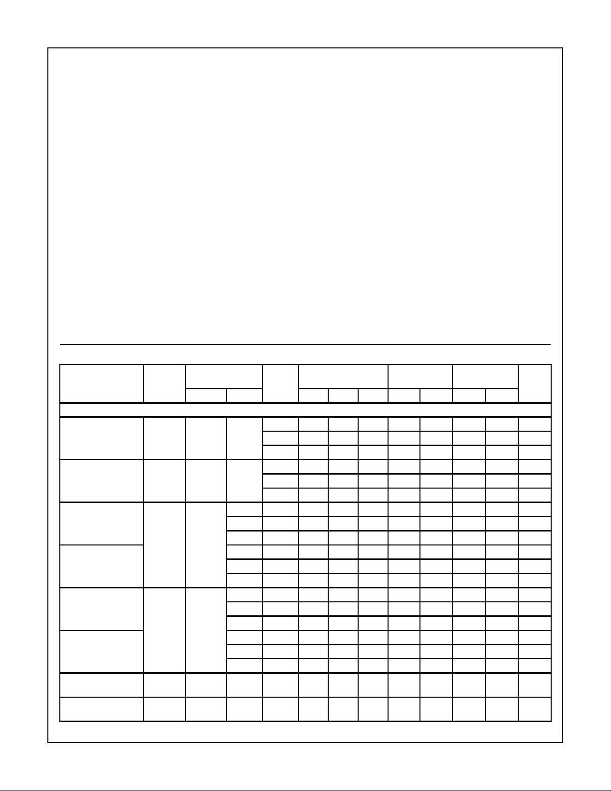
CC
DC Electrical Specifications
PARAMETER SYMBOL
HC TYPES
High Level Input
Voltage
Low Level Input
Voltage
High Level Output
Voltage
CMOS Loads
High Level Output
Voltage
TTL Loads
Low Level Output
Voltage
CMOS Loads
Low Level Output
Voltage
TTL Loads
Input Leakage
Current
Quiescent Device
Current
V
IH
V
IL
V
OH
V
OL
I
I
I
CC
TEST
CONDITIONS
(V) IO(mA) MIN TYP MAX MIN MAX MIN MAX
I
V
CC
(V)
o
C -40oC TO 85oC -55oC TO 125oC
25
UNITSV
- - 2 1.5 - - 1.5 - 1.5 - V
4.5 3.15 - - 3.15 - 3.15 - V
6 4.2 - - 4.2 - 4.2 - V
- - 2 - - 0.5 - 0.5 - 0.5 V
4.5 - - 1.35 - 1.35 - 1.35 V
6 - - 1.8 - 1.8 - 1.8 V
VIHor VIL-0.02 2 1.9 - - 1.9 - 1.9 - V
-0.02 4.5 4.4 - - 4.4 - 4.4 - V
-0.02 6 5.9 - - 5.9 - 5.9 - V
- - ---- - - - V
-4 4.5 3.98 - - 3.84 - 3.7 - V
-5.2 6 5.48 - - 5.34 - 5.2 - V
VIHor VIL0.02 2 - - 0.1 - 0.1 - 0.1 V
0.02 4.5 - - 0.1 - 0.1 - 0.1 V
0.02 6 - - 0.1 - 0.1 - 0.1 V
- - ---- - - - V
4 4.5 - - 0.26 - 0.33 - 0.4 V
5.2 6 - - 0.26 - 0.33 - 0.4 V
VCC or
-6--±0.1 - ±1-±1 µA
GND
VCC or
0 6 - - 8 - 80 - 160 µA
GND
2
CD54HC283, CD74HC283, CD54HCT283, CD74HCT283
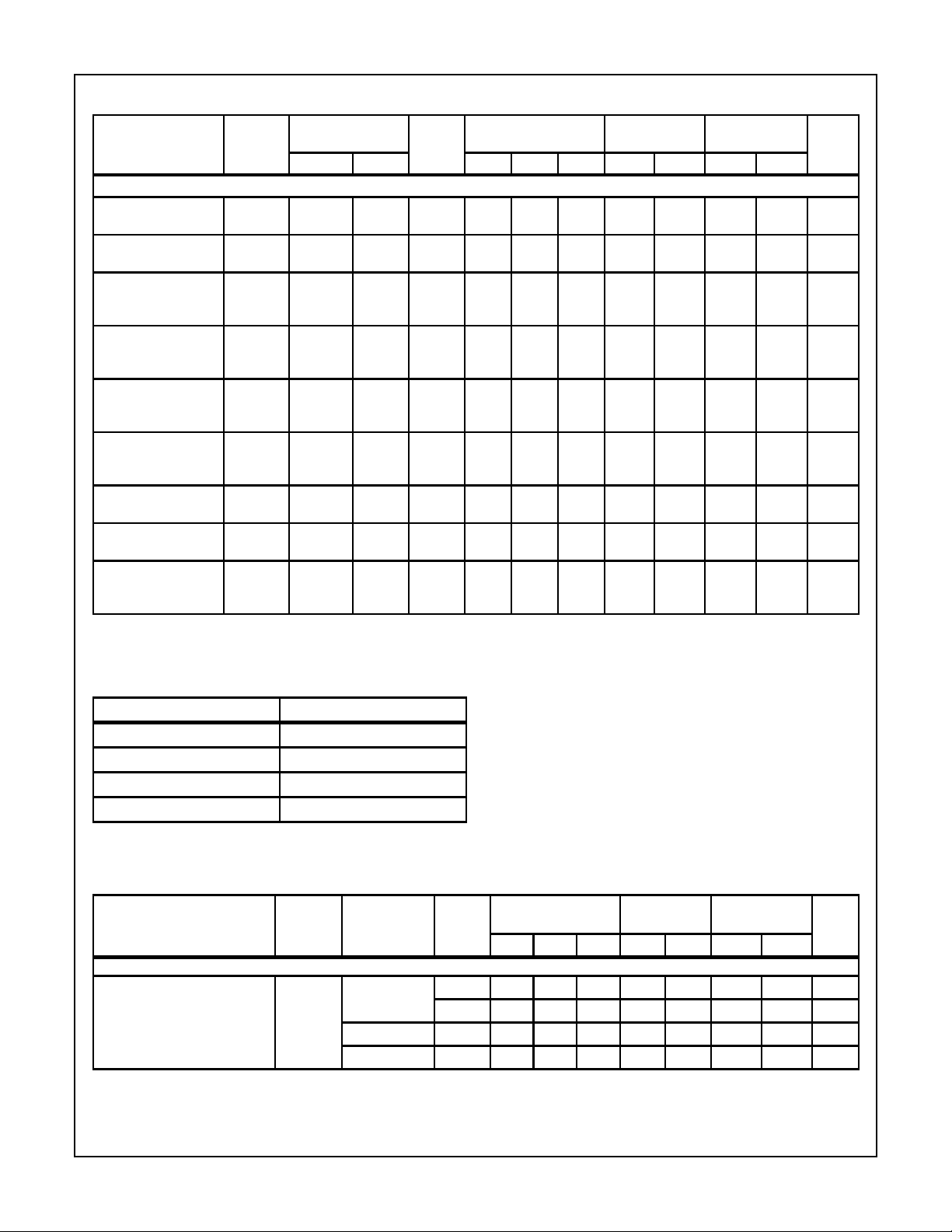
DC Electrical Specifications (Continued)
TEST
CONDITIONS
PARAMETER SYMBOL
HCT Types
High Level Input
Voltage
Low Level Input
V
IH
V
IL
Voltage
High Level Output
Voltage
V
OH
CMOS Loads
High Level Output
V
OH
Voltage
TTL Loads
Low Level Output
Voltage
V
OL
CMOS Loads
Low Level Output
Voltage
V
OL
TTL Loads
Input Leakage
Current
Quiescent Device
I
I
ICC V
Current
Additional Quiescent
Device Current Per
∆I
CC
(Note 2)
Input Pin: 1 Unit Load
NOTE:
2. For dual-supply systems theoretical worst case (V
(V) IO(mA) MIN TYP MAX MIN MAX MIN MAX
I
- - 4.5 to
- - 4.5 to
VILor VIH-0.02 4.5 4.4 - - 4.4 - 4.4 - V
VILor V
IH
VIHor VIL0.02 4.5 - - 0.1 - 0.1 - 0.1 V
VIHor V
IL
VCC to
GND
or
CC
GND
V
CC
- 2.1
o
C -40oC TO 85oC -55oC TO 125oC
V
CC
(V)
25
UNITSV
2--2- 2 - V
5.5
- - 0.8 - 0.8 - 0.8 V
5.5
-4 4.5 3.98 - - 3.84 - 3.7 - V
4 4.5 - - 0.26 - 0.33 - 0.4 V
- 5.5 - - ±0.1 - ±1-±1 µA
- 5.5 - - 8 - 80 - 160 µA
- 4.5 to
- 100 360 - 450 - 490 µA
5.5
= 2.4V, VCC = 5.5V) specification is 1.8mA.
I
HCT Input Loading Table
INPUT UNIT LOADS
C
IN
B1, A1, A0 1
B0 0.4
B3, A3, A2, B2 0.5
NOTE: Unit Load is ∆ICClimit specified in DC Electrical
Specifications table, e.g., 360µA max at 25oC.
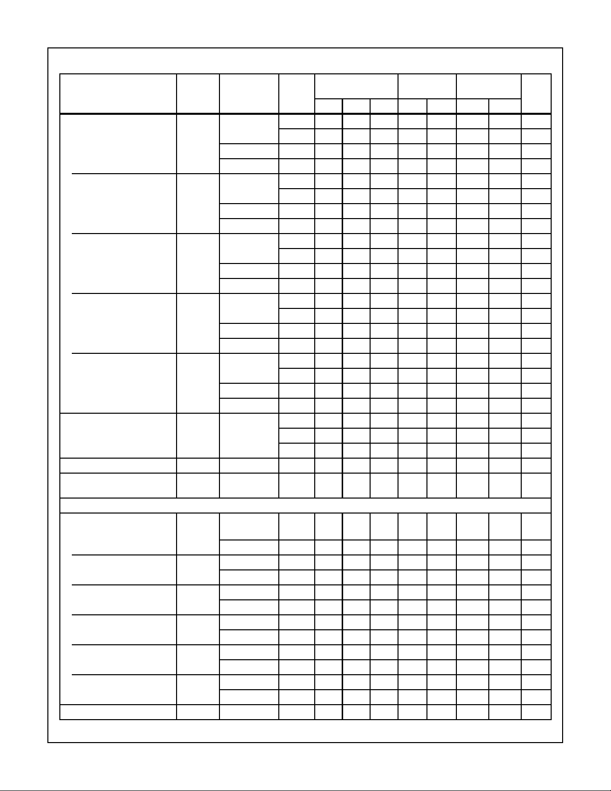
Switching Specifications Input t
r
PARAMETER SYMBOL
HC TYPES
Propagation Delay t
PLH,tPHL
CIN to S0 4.5 - - 32 - 40 - 48 ns
1.5
, tf = 6ns
TEST
CONDITIONS V
CC
(V)
25oC
-40oC TO
85oC
-55oC TO
125oC
CL= 50pF 2 - - 160 - 200 - 240 ns
CL= 15pF 5 - 13 - - - - - ns
CL= 50pF 6 - - 27 - 34 - 41 ns
UNITSMIN TYP MAX MIN MAX MIN MAX
3
CD54HC283, CD74HC283, CD54HCT283, CD74HCT283
Switching Specifications Input t
PARAMETER SYMBOL
CIN to S1 t
CIN to S2, CIN to C
OUT
CIN to S3 t
An, Bn to C
OUT
An, Bn to Sn t
Output Transition Time t
Input Capacitance C
Power Dissipation
Capacitance, (Notes 3, 4)
HCT TYPES
Propagation Delay
CIN to S0 t
CIN to S1 t
CIN to S2, CIN to C
OUT
CIN to S3 t
An, Bn to C
OUT
An, Bn to Sn t
Output Transition Time t
PLH,tPHL
t
PLH,tPHL
PLH,tPHL
t
PLH,tPHL
PLH,tPHL
TLH
C
PLH
PLH
t
PLH
PLH
t
PLH,tPH
PLH
TLH
, tf = 6ns (Continued)
r
TEST
25oC
-40oC TO
85oC
-55oC TO
125oC
CONDITIONS VCC(V)
CL= 50pF 2 - - 180 - 225 - 270 ns
4.5 - - 36 - 45 - 54 ns
CL= 15pF 5 - 15 - - - - - ns
CL= 50pF 6 - - 31 - 38 - 46 ns
CL= 50pF 2 - - 195 - 245 - 295 ns
4.5 - - 39 - 49 - 59 ns
CL= 15pF 5 - 16 - - - - - ns
CL= 50pF 6 - - 33 - 42 - 50 ns
CL= 50pF 2 - - 230 - 290 - 345 ns
4.5 - - 46 - 58 - 69 ns
CL= 15pF 5 - 19 - - - - - ns
CL= 50pF 6 - - 39 - 49 - 59 ns
CL= 50pF 2 - - 195 - 245 - 295 ns
4.5 - - 39 - 49 - 59 ns
CL= 15pF 5 - 16 - - - - - ns
CL= 50pF 6 - - 33 - 42 - 50 ns
CL= 50pF 2 - - 210 - 265 - 315 ns
4.5 - - 42 - 53 - 63 ns
CL= 15pF 5 - 18 - - - - - ns
CL= 50pF 6 - - 36 - 45 - 54 ns
, t
CL= 50pF 2 - - 75 - 95 - 110 ns
THL
4.5 - - 15 - 19 - 22 ns
6 - - 13 - 16 - 19 ns
IN
PD
, t
CL= 50pF - - - 10 - 10 - 10 pF
-5-70-----pF
CL= 15pF 5 - 13 - - - - - ns
PHL
CL= 50pF 4.5 - - 31 - 39 - 47 ns
, t
CL= 15pF 5 - 18 - - - - - ns
PHL
CL= 50pF 4.5 - 43 - 54 - 65 ns
, t
CL= 15pF 5 - 19 - - - - - ns
PHL
CL= 50pF 4.5 - 46 - 58 - 69 ns
, t
CL= 15pF 5 - 22 - - - - - ns
PHL
CL= 50pF 4.5 - 53 - 66 - 80 ns
LCL= 15pF 5 - 20 - - - - - ns
CL= 50pF 4.5 - 48 - 60 - 72 ns
, t
CL= 15pF 5 - 21 - - - - - ns
PHL
CL= 50pF 4.5 - 49 - 61 - 74 ns
, t
CL= 50pF 4.5 - 15 - 19 - 22 ns
THL
UNITSMIN TYP MAX MIN MAX MIN MAX
4

CD54HC283, CD74HC283, CD54HCT283, CD74HCT283
Switching Specifications Input t
, tf = 6ns (Continued)
r
TEST
PARAMETER SYMBOL
Input Capacitance C
Power Dissipation
C
CONDITIONS VCC(V)
IN
PD
- - - - 10 - 10 - 10 pF
-5-82-----pF
Capacitance, (Notes 3, 4)
NOTES:
3. CPD is used to determine the dynamic power consumption, per package.
4. PD = V
2
fi(CPD + CL) where: fi = Input Frequency, CL = Output Load Capacitance, VCC = Supply Voltage.
CC
Test Circuits and Waveforms
tr = 6ns tf = 6ns
V
t
CC
GND
TLH
INPUT
t
INVERTING
OUTPUT
THL
t
PHL
90%
50%
10%
t
90%
50%
10%
PLH
25oC
tr = 6ns
INPUT
t
INVERTING
OUTPUT
THL
t
PHL
-40oC TO
85oC
2.7V
1.3V
0.3V
t
PLH
-55oC TO
125oC
= 6ns
t
f
90%
1.3V
10%
t
TLH
UNITSMIN TYP MAX MIN MAX MIN MAX
3V
GND
FIGURE 1. HC AND HCU TRANSITION TIMES AND PROPAGA-
TION DELAY TIMES, COMBINATION LOGIC
FIGURE 2. HCT TRANSITION TIMES AND PROPAGATION
DELAY TIMES, COMBINATION LOGIC
5

PACKAGE OPTION ADDENDUM
www.ti.com
1-Jul-2005
PACKAGING INFORMATION
Orderable Device Status
(1)
Package
Type
Package
Drawing
Pins Package
Qty
Eco Plan
5962-8976501EA ACTIVE CDIP J 16 1 TBD Call TI Level-NC-NC-NC
CD54HC283F3A ACTIVE CDIP J 16 1 TBD Call TI Level-NC-NC-NC
CD54HCT283F3A ACTIVE CDIP J 16 1 TBD Call TI Level-NC-NC-NC
CD74HC283E ACTIVE PDIP N 16 25 Pb-Free
CD74HC283M ACTIVE SOIC D 16 40 Green (RoHS &
no Sb/Br)
CD74HC283M96 ACTIVE SOIC D 16 2500 Green (RoHS &
no Sb/Br)
CD74HC283M96E4 ACTIVE SOIC D 16 2500 Green (RoHS &
no Sb/Br)
CD74HC283ME4 ACTIVE SOIC D 16 40 Green (RoHS &
no Sb/Br)
CD74HC283MT ACTIVE SOIC D 16 250 Green (RoHS &
no Sb/Br)
CD74HC283MTE4 ACTIVE SOIC D 16 250 Green (RoHS &
no Sb/Br)
CD74HCT283E ACTIVE PDIP N 16 25 Pb-Free
CD74HCT283EE4 ACTIVE PDIP N 16 25 Pb-Free
CD74HCT283M ACTIVE SOIC D 16 40 Green (RoHS &
no Sb/Br)
CD74HCT283M96 ACTIVE SOIC D 16 2500 Green (RoHS &
no Sb/Br)
CD74HCT283M96E4 ACTIVE SOIC D 16 2500 Green (RoHS &
no Sb/Br)
CD74HCT283ME4 ACTIVE SOIC D 16 40 Green (RoHS &
no Sb/Br)
CD74HCT283MT ACTIVE SOIC D 16 250 Green (RoHS &
no Sb/Br)
CD74HCT283MTE4 ACTIVE SOIC D 16 250 Green (RoHS &
no Sb/Br)
(1)
The marketing status values are defined as follows:
ACTIVE: Product device recommended for new designs.
LIFEBUY: TI has announced that the device will be discontinued, and a lifetime-buy period is in effect.
NRND: Not recommended for new designs. Device is in production to support existing customers, but TI does not recommend using this part in
a new design.
PREVIEW: Device has been announced but is not in production. Samples may or may not be available.
OBSOLETE: TI has discontinued the production of the device.
(RoHS)
(RoHS)
(RoHS)
(2)
Lead/Ball Finish MSL Peak Temp
CU NIPDAU Level-NC-NC-NC
CU NIPDAU Level-1-260C-UNLIM
CU NIPDAU Level-1-260C-UNLIM
CU NIPDAU Level-1-260C-UNLIM
CU NIPDAU Level-1-260C-UNLIM
CU NIPDAU Level-1-260C-UNLIM
CU NIPDAU Level-1-260C-UNLIM
CU NIPDAU Level-NC-NC-NC
CU NIPDAU Level-NC-NC-NC
CU NIPDAU Level-1-260C-UNLIM
CU NIPDAU Level-1-260C-UNLIM
CU NIPDAU Level-1-260C-UNLIM
CU NIPDAU Level-1-260C-UNLIM
CU NIPDAU Level-1-260C-UNLIM
CU NIPDAU Level-1-260C-UNLIM
(3)
(2)
Eco Plan - The planned eco-friendly classification: Pb-Free (RoHS) or Green (RoHS & no Sb/Br) - please check
http://www.ti.com/productcontent for the latest availability information and additional product content details.
TBD: The Pb-Free/Green conversion plan has not been defined.
Pb-Free (RoHS): TI's terms "Lead-Free" or "Pb-Free" mean semiconductor products that are compatible with the current RoHS requirements
for all 6 substances, including the requirement that lead not exceed 0.1% by weight in homogeneous materials. Where designed to be soldered
at high temperatures, TI Pb-Free products are suitable for use in specified lead-free processes.
Green (RoHS & no Sb/Br): TI defines "Green" to mean Pb-Free (RoHS compatible), and free of Bromine (Br) and Antimony (Sb) based flame
retardants (Br or Sb do not exceed 0.1% by weight in homogeneous material)
(3)
MSL, Peak Temp. -- The Moisture Sensitivity Level rating according to the JEDEC industry standard classifications, and peak solder
Addendum-Page 1

PACKAGE OPTION ADDENDUM
www.ti.com
temperature.
Important Information and Disclaimer:The information provided on this page represents TI's knowledge and belief as of the date that it is
provided. TI bases its knowledge and belief on information provided by third parties, and makes no representation or warranty as to the
accuracy of such information. Efforts are underway to better integrate information from third parties. TI has taken and continues to take
reasonable steps to provide representative and accurate information but may not have conducted destructive testing or chemical analysis on
incoming materials and chemicals. TI and TI suppliers consider certain information to be proprietary, and thus CAS numbers and other limited
information may not be available for release.
In no event shall TI's liability arising out of such information exceed the total purchase price of the TI part(s) at issue in this document sold by TI
to Customer on an annual basis.
1-Jul-2005
Addendum-Page 2


IMPORTANT NOTICE
Texas Instruments Incorporated and its subsidiaries (TI) reserve the right to make corrections, modifications,
enhancements, improvements, and other changes to its products and services at any time and to discontinue
any product or service without notice. Customers should obtain the latest relevant information before placing
orders and should verify that such information is current and complete. All products are sold subject to TI’s terms
and conditions of sale supplied at the time of order acknowledgment.
TI warrants performance of its hardware products to the specifications applicable at the time of sale in
accordance with TI’s standard warranty. Testing and other quality control techniques are used to the extent TI
deems necessary to support this warranty . Except where mandated by government requirements, testing of all
parameters of each product is not necessarily performed.
TI assumes no liability for applications assistance or customer product design. Customers are responsible for
their products and applications using TI components. To minimize the risks associated with customer products
and applications, customers should provide adequate design and operating safeguards.
TI does not warrant or represent that any license, either express or implied, is granted under any TI patent right,
copyright, mask work right, or other TI intellectual property right relating to any combination, machine, or process
in which TI products or services are used. Information published by TI regarding third-party products or services
does not constitute a license from TI to use such products or services or a warranty or endorsement thereof.
Use of such information may require a license from a third party under the patents or other intellectual property
of the third party, or a license from TI under the patents or other intellectual property of TI.
Reproduction of information in TI data books or data sheets is permissible only if reproduction is without
alteration and is accompanied by all associated warranties, conditions, limitations, and notices. Reproduction
of this information with alteration is an unfair and deceptive business practice. TI is not responsible or liable for
such altered documentation.
Resale of TI products or services with statements different from or beyond the parameters stated by TI for that
product or service voids all express and any implied warranties for the associated TI product or service and
is an unfair and deceptive business practice. TI is not responsible or liable for any such statements.
Following are URLs where you can obtain information on other Texas Instruments products and application
solutions:
Products Applications
Amplifiers amplifier.ti.com Audio www.ti.com/audio
Data Converters dataconverter.ti.com Automotive www.ti.com/automotive
DSP dsp.ti.com Broadband www.ti.com/broadband
Interface interface.ti.com Digital Control www.ti.com/digitalcontrol
Logic logic.ti.com Military www.ti.com/military
Power Mgmt power.ti.com Optical Networking www.ti.com/opticalnetwork
Microcontrollers microcontroller.ti.com Security www.ti.com/security
Telephony www.ti.com/telephony
Video & Imaging www.ti.com/video
Wireless www.ti.com/wireless
Mailing Address: Texas Instruments
Post Office Box 655303 Dallas, Texas 75265
Copyright 2005, Texas Instruments Incorporated
 Loading...