

Texas Instruments CD74HCT173E, CD74HCT173M96, CD74HCT173M, CD74HC173M96, CD74HC173M Datasheet
...
CD74HC173,
/
[ /Title
(CD74H
C173,
CD74H
CT173)
Subject
(High
Speed
CMOS
Logic
Quad DType
Data sheet acquired from Harris Semiconductor
SCHS158
February 1998
Features
• Three-State Buffered Outputs
• Gated Input and Output Enables
• Fanout (Over Temperature Range)
- Standard Outputs. . . . . . . . . . . . . . . 10 LSTTL Loads
- Bus Driver Outputs . . . . . . . . . . . . . 15 LSTTL Loads
• Wide Operating Temperature Range . . . -55
• Balanced Propagation Delay and Transition Times
• Significant Power Reduction Compared to LSTTL
Logic ICs
• HC Types
- 2V to 6V Operation
- High Noise Immunity: N
at VCC = 5V
• HCT Types
- 4.5V to 5.5V Operation
- Direct LSTTL Input Logic Compatibility,
V
= 0.8V (Max), VIH = 2V (Min)
IL
- CMOS Input Compatibility, I
= 30%, NIH = 30% of V
IL
≤ 1µA at VOL, V
l
o
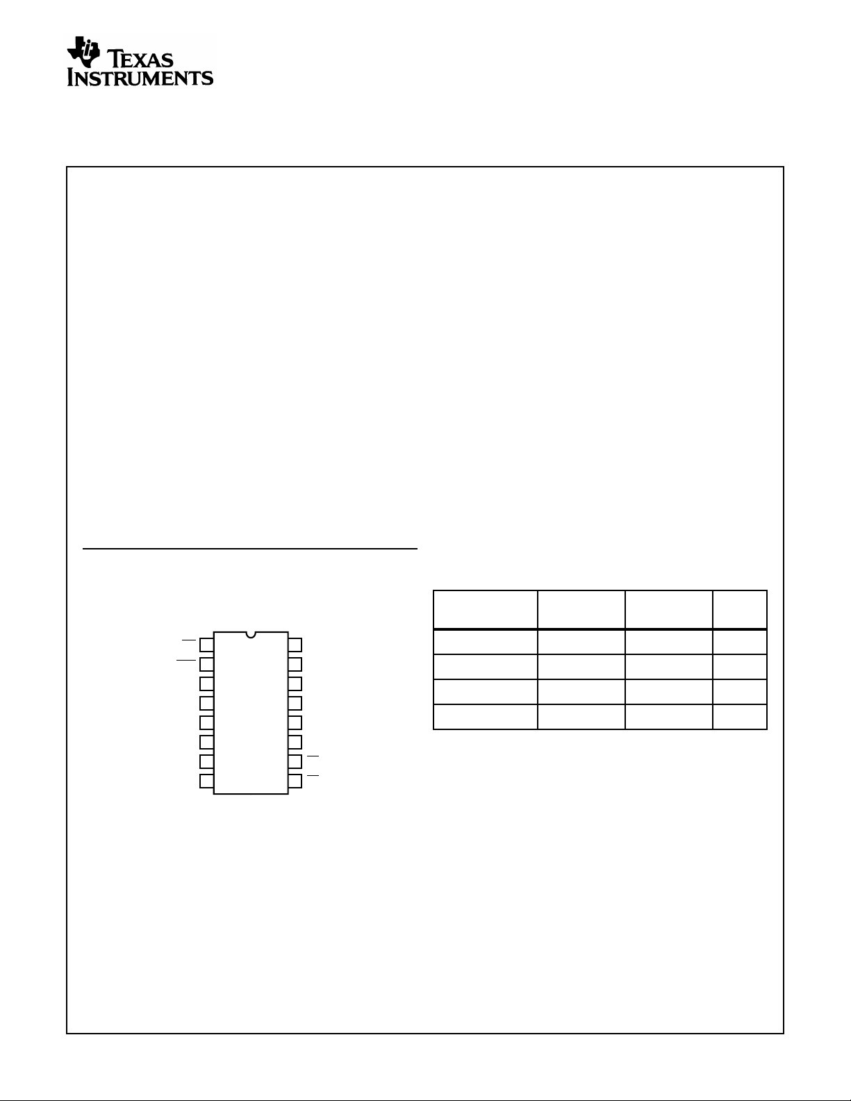
Pinout
CD74HC173, CD74HC173
(PDIP, SOIC)
TOP VIEW
C to 125oC
CC
OH
CD74HCT173
High Speed CMOS Logic
Quad D-Type Flip-Flop, Three-State
Description
The Harris CD74HC173 and CD74HCT173 high speed
three-state quad D-type flip-flops are fabricated with silicon
gate CMOS technology. They possess the low power consumption of standard CMOS Integrated circuits, and can
operate at speeds comparable to the equivalent low power
Schottky devices. The buffered outputs can drive 15 LSTTL
loads. The large output drive capability and three-state feature make these parts ideally suited for interfacing with bus
lines in bus oriented systems.
The four D-typeflip-flops operate synchronously from a common clock. The outputs are in the three-state mode when
either of the two output disable pins are at the logic “1” level.
The input ENABLES allow the flip-flops to remain in their
present states without having to disrupt the clock If either of
the 2 input ENABLES are taken to a logic “1” level, the Q
outputs are fed back to the inputs, forcing the flip-flops to
remain in the same state. Reset is enabled by taking the
MASTER RESET (MR) input to a logic “1” level. The data
outputs change state on the positive going edge of the clock.
The CD74HCT173 logic family is functionally, as well as pin
compatible with the standard 74LS logic family
Ordering Information
TEMP.RANGE
PART NUMBER
(oC) PACKAGE
.
PKG.
NO.
OE
OE2
Q
Q
Q
Q
CP
GND
V
1
2
3
0
4
1
5
2
6
3
7
8
16
CC
MR
15
14
D0
13
D1
D2
12
D3
11
E2
10
9
E1
CD74HC173E -55 to 125 16 Ld PDIP E16.3
CD74HCT173E -55 to 125 16 Ld PDIP E16.3
CD74HC173M -55 to 125 16 Ld SOIC M16.15
CD74HCT173M -55 to 125 16 Ld SOIC M16.15
NOTES:
1. When ordering, use the entire part number.Add the suffix 96 to
obtain the variant in the tape and reel.
2. Wafer and die for this part number is available which meets all
electrical specifications. Please contact your local sales office or
Harris customer service for ordering information.
CAUTION: These devices are sensitive to electrostatic discharge. Users should follow proper IC Handling Procedures.
Copyright
© Harris Corporation 1998
1
File Number 1641.1
Functional Diagram
E1
E2
14
D0
13
D1
12
D2
11
D3
7
CP
MR
OE1
OE2
TRUTH TABLE
INPUTS
CD74HC173, CD74HCT173
10
9
3
Q
0
4
Q
1
5
Q
2
6
Q
3
2
115
DATA OUTPUT
n
MR CP
DATA ENABLE
E1 E2 D Q
HXXXXL
LLXXXQ
L↑HXXQ
L↑XHXQ
0
0
0
L↑LLLL
L↑LLHH
NOTE:
When either OE1 or OE2 (or both) is (are) high the output isdisabled
to the high-impedance state, however, sequential operation of the
flip-flops is not affected.
H = High Voltage Level
L = Low Voltage Level
X = Irrelevant
↑ = Transition from Low to High Level
Q0= Level Before the Indicated Steady-State Input Conditions Were
Established
2
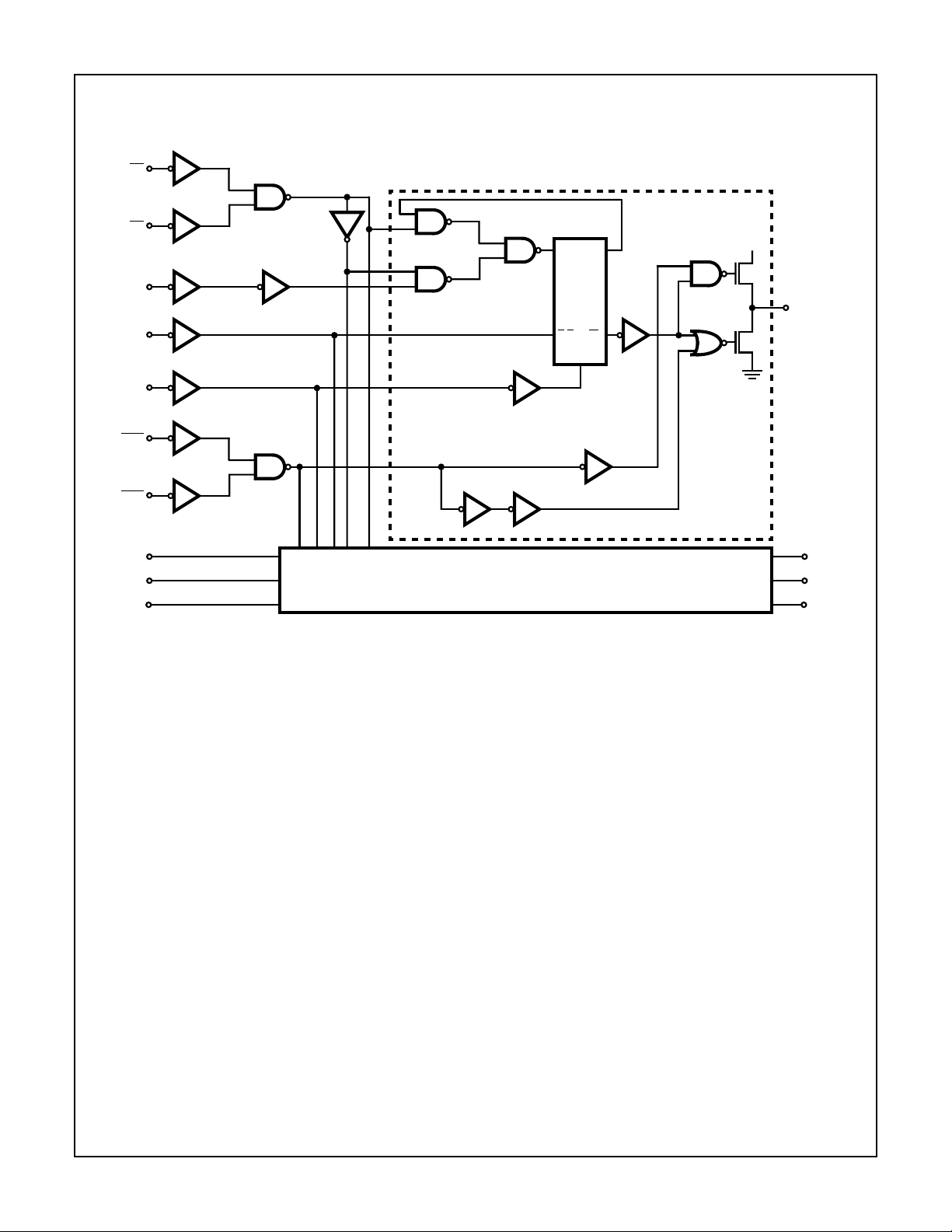
Logic Diagram
9
E1
10
E2
14
D0
7
CP
15
MR
1
OE1
2
OE2
CD74HC173, CD74HCT173
DQ
CP Q
R
V
CC
P
3
Q
0
N
D1
D2
D3
13
12
11
3 CIRCUITS IDENTICAL TO ABOVE CIRCUIT
IN DASHED ENCLOSURE
4
Q
1
5
Q
2
6
Q
3
3

CD74HC173, CD74HCT173
Absolute Maximum Ratings Thermal Information
DC Supply Voltage, VCC. . . . . . . . . . . . . . . . . . . . . . . . -0.5V to 7V
DC Input Diode Current, I
IK
For VI < -0.5V or VI > VCC + 0.5V. . . . . . . . . . . . . . . . . . . . . .±20mA
DC Output Diode Current, I
OK
For VO < -0.5V or VO > VCC + 0.5V . . . . . . . . . . . . . . . . . . . .±20mA
DC Output Source or Sink Current per Output Pin, I
O
For VO > -0.5V or VO < VCC + 0.5V . . . . . . . . . . . . . . . . . . . .±25mA
DC VCC or Ground Current, ICC . . . . . . . . . . . . . . . . . . . . . . . . .±70mA
Operating Conditions
Temperature Range (TA) . . . . . . . . . . . . . . . . . . . . . -55oC to 125oC
Supply Voltage Range, V
HC Types . . . . . . . . . . . . . . . . . . . . . . . . . . . . . . . . . . . . .2V to 6V
HCT Types . . . . . . . . . . . . . . . . . . . . . . . . . . . . . . . . .4.5V to 5.5V
DC Input or Output Voltage, VI, VO . . . . . . . . . . . . . . . . . 0V to V
Input Rise and Fall Time
2V . . . . . . . . . . . . . . . . . . . . . . . . . . . . . . . . . . . . . . 1000ns (Max)
4.5V. . . . . . . . . . . . . . . . . . . . . . . . . . . . . . . . . . . . . . 500ns (Max)
6V . . . . . . . . . . . . . . . . . . . . . . . . . . . . . . . . . . . . . . . 400ns (Max)
CAUTION: Stresses above those listed in “Absolute Maximum Ratings” may cause permanent damage to the device. This is a stress only rating and operation
of the device at these or any other conditions above those indicated in the operational sections of this specification is not implied.
NOTE:
3. θJA is measured with the component mounted on an evaluation PC board in free air.
CC
Thermal Resistance (Typical, Note 3) θJA (oC/W)
PDIP Package. . . . . . . . . . . . . . . . . . . . . . . . . . . . . 90
SOIC Package. . . . . . . . . . . . . . . . . . . . . . . . . . . . . 160
Maximum Junction Temperature . . . . . . . . . . . . . . . . . . . . . . .150oC
Maximum Storage Temperature Range . . . . . . . . . .-65oC to 150oC
Maximum Lead Temperature (Soldering 10s) . . . . . . . . . . . . .300oC
(SOIC - Lead Tips Only)
CC
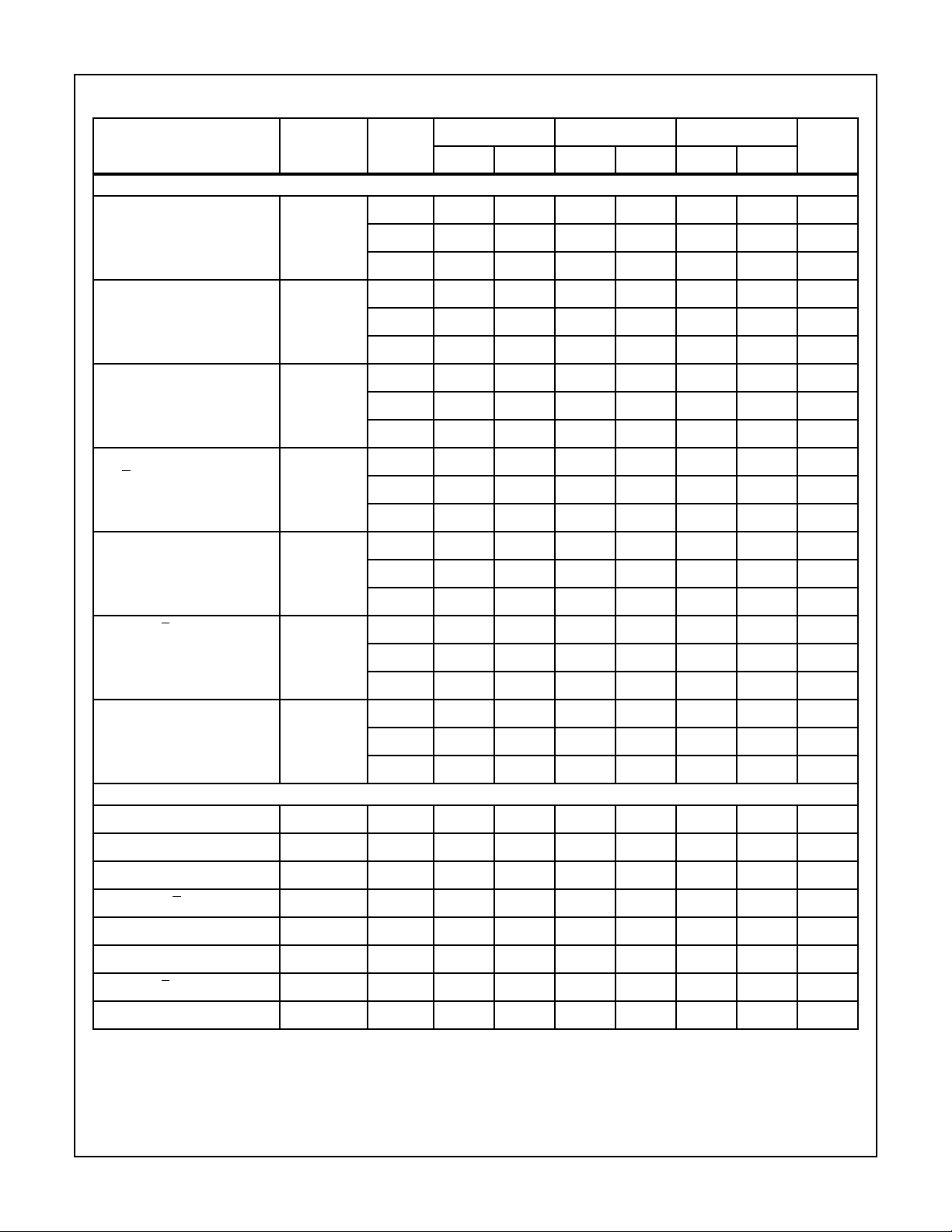
DC Electrical Specifications
PARAMETER SYMBOL
HC TYPES
High Level Input
Voltage
Low Level Input
Voltage
High Level Output
Voltage
CMOS Loads
High Level Output
Voltage
TTL Loads
Low Level Output
Voltage
CMOS Loads
Low Level Output
Voltage
TTL Loads
Input Leakage
Current
Quiescent Device
Current
V
IH
V
IL
V
OH
V
OL
I
I
I
CC
TEST
CONDITIONS
25oC -40oC TO 85oC -55oC TO 125oC
VCC (V)
- - 2 1.5 - - 1.5 - 1.5 - V
4.5 3.15 - - 3.15 - 3.15 - V
6 4.2 - - 4.2 - 4.2 - V
- - 2 - - 0.5 - 0.5 - 0.5 V
4.5 - - 1.35 - 1.35 - 1.35 V
6 - - 1.8 - 1.8 - 1.8 V
VIH or
V
-0.02 2 1.9 - - 1.9 - 1.9 - V
IL
-0.02 4.5 4.4 - - 4.4 - 4.4 - V
-0.02 6 5.9 - - 5.9 - 5.9 - V
-6 4.5 3.98 - - 3.84 - 3.7 - V
-7.8 6 5.48 - - 5.34 - 5.2 - V
VIH or
V
0.02 2 - - 0.1 - 0.1 - 0.1 V
IL
0.02 4.5 - - 0.1 - 0.1 - 0.1 V
0.02 6 - - 0.1 - 0.1 - 0.1 V
6 4.5 - - 0.26 - 0.33 - 0.4 V
7.8 6 - - 0.26 - 0.33 - 0.4 V
VCC or
-6--±0.1 - ±1-±1µA
GND
VCC or
0 6 - - 8 - 80 - 160 µA
GND
UNITSVI(V) IO(mA) MIN TYP MAX MIN MAX MIN MAX
4
CD74HC173, CD74HCT173
DC Electrical Specifications (Continued)
TEST
CONDITIONS
PARAMETER SYMBOL
Three-State Leakage
Current
I
OZ
VIL or
V
IH
V
(V)
CC
-6--±0.5 - ±0.5 - ±10 µA
HCT TYPES
High Level Input
Voltage
Low Level Input
Voltage
High Level Output
Voltage
V
IH
- - 4.5 to
5.5
V
IL
- - 4.5 to
5.5
V
OH
VIH or
V
IL
-0.02 4.5 4.4 - - 4.4 - 4.4 - V
CMOS Loads
High Level Output
-6 4.5 3.98 - - 3.84 - 3.7 - V
Voltage
TTL Loads
Low Level Output
Voltage
V
OL
VIH or
V
IL
0.02 4.5 - - 0.1 - 0.1 - 0.1 V
CMOS Loads
Low Level Output
6 4.5 - - 0.26 - 0.33 - 0.4 V
Voltage
TTL Loads
Input Leakage
Current
Quiescent Device
Current
Additional Quiescent
Device Current Per
I
VCC to
I
0 5.5 - - ±0.1 - ±1-±1µA
GND
I
CC
VCC or
0 5.5 - - 8 - 80 - 160 µA
GND
∆I
CC
V
-2.1
CC
- 4.5 to
5.5
Input Pin: 1 Unit Load
(Note 4)
Three-State Leakage
Current
I
OZ
VIL or
V
IH
- 5.5 - - ±0.5 - ±5.0 - ±10 µA
NOTE:
4. For dual-supply systems theoretical worst case (VI = 2.4V, VCC = 5.5V) specification is 1.8mA.
25oC -40oC TO 85oC -55oC TO 125oC
2-- 2 - 2 - V
- - 0.8 - 0.8 - 0.8 V
- 100 360 - 450 - 490 µA
UNITSVI(V) IO(mA) MIN TYP MAX MIN MAX MIN MAX
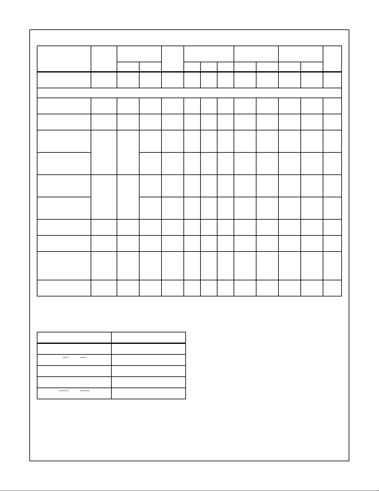
HCT Input Loading Table
INPUT UNIT LOADS
D0-D3 0.15
E1 and E2 0.15
CP 0.25
MR 0.2
OE1 and OE2 0.5
NOTE: Unit Load is ∆ICClimit specified in DC Electrical
Specifications table, e.g., 360µA max at 25oC.
5

CD74HC173, CD74HCT173
Switching Specifications Input t
, tf = 6ns
r
TEST
PARAMETER SYMBOL
CONDITIONS VCC (V)
HC TYPES
Propagation Delay, Clock to
Output
t
PLH
, t
PHLCL
= 50pF 2 - 200 250 300 ns
4.5 - 40 50 60 ns
CL= 15pF 5 17 - - - ns
CL = 50pF 6 - 34 43 51 ns
Propagation Delay, MR to
Output
t
PHL
CL= 50pF 2 - 175 220 265 ns
4.5 - 35 44 53 ns
CL= 15pF 5 12 - - - ns
CL = 50pF 6 - 30 37 45 ns
Propagation Delay Output
Enable to Q (Figure 6)
t
t
PLZ
PZL
, t
, t
CL = 50pF 2 150 190 225 ns
PHZ
PZH
CL= 50pF 4.5 30 38 45 ns
CL= 15pF 5 12 - - - ns
CL = 50pF 6 26 33 38 ns
Output Transition Times t
TLH
, t
THLCL
= 50pF 2 - 60 75 90 ns
4.5 - 12 15 18 ns
6 - 10 13 15 ns
Maximum Clock Frequency f
Input Capacitance C
Three-State Output
MAX
IN
C
O
CL= 15pF 5 60 - - - MHz
---1010 10pF
---1010 10pF
Capacitance
Power Dissipation
C
PD
- 5 29 - - - pF
Capacitance
(Notes 5, 6)
HCT TYPES
Propagation Delay, Clock to
Output
Propagation Delay, MR to
Output
Propagation Delay Output
Enable to Q (Figure 6)
t
t
PLH
PZL
, t
PHLCL
t
PHL
, t
PZH
= 50pF 4.5 - 40 50 60 ns
CL= 15pF 5 17 - - - ns
CL= 50pF 4.5 - 44 55 66 ns
CL= 15pF 5 18 - - - ns
CL = 50pF 2 150 190 225 ns
CL= 50pF 4.5 30 38 45 ns
CL= 15pF 5 14 - - - ns
CL = 50pF 6 26 33 38 ns
Output Transition Times t
Maximum Clock Frequency f
Input Capacitance C
Power Dissipation
TLH
C
, t
THLCL
MAX
IN
PD
= 50pF 4.5 - 15 19 22 ns
CL= 15pF 5 60 - - - MHz
---1010 10pF
- 5 34 - - - pF
Capacitance
(Notes 5, 6)
NOTES:
5. CPD is used to determine the dynamic power consumption, per package.
6. PD=V
CC
2
fi+∑ (CLV
2
+fO)where fi=Input Frequency,fO=Input Frequency,CL=Output LoadCapacitance, VCC=Supply Voltage.
CC
25oC -40oC TO 85oC -55oCTO125oC
UNITSTYP MAX MAX MAX
6
CD74HC173, CD74HCT173
Prerequisite For Switching Specifications
25oC -40oC TO 85oC -55oC TO 125oC
PARAMETER SYMBOL VCC (V)
HC TYPES
Maximum Clock Frequency f
MR Pulse Width t
Clock Pulse Width t
Set-up Time, Data to Clock
and E to Clock
Hold Time, Data to Clock t
MAX
w
w
t
SU
H
UNITSMIN MAX MIN MAX MIN MAX
26-5-4-MHz
4.5 30 - 24 - 20 - MHz
6 35 - 28 - 24 - MHz
2 80 - 100 - 120 - ns
4.5 16 - 20 - 24 - ns
614-17-20-ns
2 80 - 100 - 120 - ns
4.5 16 - 20 - 24 - ns
614-17-20-ns
260-75-90-ns
4.5 12 - 15 - 18 - ns
610-13-15-ns
23-3-3-ns
4.5 3 - 3 - 3 - ns
63-3-3-ns
Hold Time, E to Clock t
Removal Time, MR to Clock t
HCT TYPES
Maximum Clock Frequency f
MR Pulse Width t
Clock Pulse Width t
Set-up Time, E to Clock t
Set-up Time, Data to Clock t
Hold Time, Data to Clock t
Hold Time, E to Clock t
Removal Time, MR to Clock t
H
REM
MAX
w
w
SU
SU
H
H
REM
20-0-0-ns
4.5 0 - 0 - 0 - ns
60-0-0-ns
260-75-90-ns
4.5 12 - 15 - 18 - ns
610-13-15-ns
4.5 20 - 16 - 13 - MHz
4.5 15 - 19 - 22 - ns
4.5 25 - 31 - 38 - ns
4.5 12 - 15 - 18 - ns
4.5 18 - 23 - 27 - ns
4.5 0 - 0 - 0 - ns
4.5 0 - 0 - 0 - ns
4.5 12 - 15 - 18 - ns
7
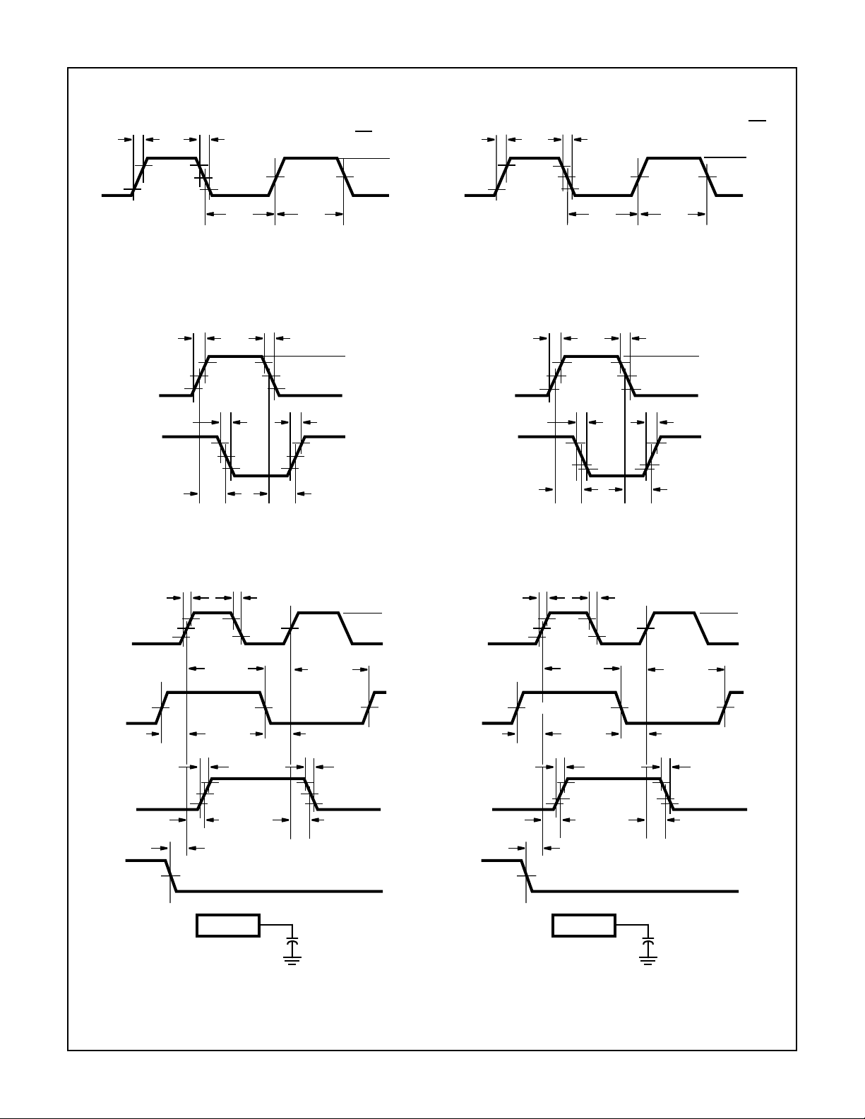
Test Circuits and Waveforms
trC
L
CLOCK
10%
90%
50%
10%
tfC
t
L
WL
tWL+ tWH=
50%
t
CD74HC173, CD74HCT173
WH
f
CL
50%
I
V
CC
GND
t
rCL
CLOCK
= 6ns
0.3V
2.7V
1.3V
0.3V
t
t
fCL
WL
= 6ns
1.3V
t
WL
+ tWH=
I
fC
L
3V
1.3V
GND
t
WH
NOTE: Outputs should be switching from 10% VCC to 90% VCC in
accordance with device truth table.For f
, input duty cycle = 50%.
MAX
FIGURE 1. HC CLOCK PULSE RISE AND FALLTIMES AND
PULSE WIDTH
tr = 6ns tf = 6ns
V
t
CC
GND
TLH
INPUT
t
90%
50%
10%
THL
90%
t
50%
10%
PLH
INVERTING
OUTPUT
t
PHL
FIGURE 3. HC AND HCU TRANSITION TIMES AND PROPAGA-
TION DELAY TIMES, COMBINATION LOGIC
tfC
L
V
CC
50%
GND
t
H(L)
V
CC
50%
t
SU(L)
GND
CLOCK
INPUT
DAT A
INPUT
t
SU(H)
trC
L
90%
10%
t
H(H)
NOTE: Outputs should be switching from 10% VCC to 90% VCC in
accordance with device truth table.For f
, input duty cycle = 50%.
MAX
FIGURE 2. HCT CLOCK PULSE RISE AND FALLTIMES AND
PULSE WIDTH
= 6ns
tr = 6ns
INPUT
t
2.7V
1.3V
0.3V
THL
t
f
3V
GND
t
TLH
90%
t
PLH
1.3V
10%
INVERTING
OUTPUT
t
PHL
FIGURE 4. HCT TRANSITION TIMES AND PROPAGATION
DELAY TIMES, COMBINATION LOGIC
CLOCK
INPUT
DAT A
INPUT
t
SU(H)
trC
L
2.7V
0.3V
t
H(H)
1.3V
1.3V
tfC
L
3V
1.3V
GND
t
H(L)
3V
1.3V
t
SU(L)
GND
OUTPUT
t
REM
V
CC
SET, RESET
OR PRESET
50%
90%
t
PLH
IC
t
TLH
t
THL
90%
50%
10%
t
PHL
GND
C
L
50pF
FIGURE 5. HC SETUP TIMES, HOLD TIMES, REMOVAL TIME,
AND PROPAGATION DELAY TIMES FOR EDGE
TRIGGERED SEQUENTIAL LOGIC CIRCUITS
OUTPUT
t
REM
3V
SET, RESET
1.3V
90%
1.3V
t
t
PLH
TLH
90%
1.3V
10%
t
t
PHL
THL
OR PRESET
IC
C
L
50pF
FIGURE 6. HCT SETUP TIMES, HOLD TIMES, REMOVAL TIME,
AND PROPAGATION DELAY TIMES FOR EDGE
TRIGGERED SEQUENTIAL LOGIC CIRCUITS
8
GND

Test Circuits and Waveforms
(Continued)
6ns 6ns
OUTPUT
DISABLE
OUTPUT LOW
TO OFF
OUTPUT HIGH
TO OFF
50%
t
t
OUTPUTS
ENABLED
PLZ
PHZ
10%
90%
90%
10%
t
PZL
t
PZH
OUTPUTS
DISABLED
FIGURE 7. HC THREE-STATE PROPAGATION DELAY
WAVEFORM
OTHER
INPUTS
TIED HIGH
OR LOW
OUTPUT
DISABLE
NOTE: Open drain waveforms t
PLZ
and t
are the same as those for three-state shown on the left. The test circuit is Output RL=1kΩto
PZL
VCC, CL = 50pF.
FIGURE 9. HC AND HCT THREE-STATE PROPAGATION DELAY TEST CIRCUIT
50%
50%
OUTPUTS
ENABLED
IC WITH
THREE-
STATE
OUTPUT
V
CC
GND
OUTPUT
R
0.3
t
t
6ns
PZL
PZH
t
r
OUTPUT
DISABLE
OUTPUT LOW
TO OFF
OUTPUT HIGH
TO OFF
t
t
OUTPUTS
ENABLED
6ns t
PLZ
PHZ
10%
90%
f
2.7
1.3
OUTPUTS
DISABLED
FIGURE 8. HCT THREE-STATE PROPAGATION DELAY
WAVEFORM
= 1kΩ
L
C
L
50pF
VCC FOR t
GND FOR t
PLZ
PHZ
AND t
AND t
PZL
PZH
3V
GND
1.3V
1.3V
OUTPUTS
ENABLED
9

IMPORTANT NOTICE
T exas Instruments and its subsidiaries (TI) reserve the right to make changes to their products or to discontinue
any product or service without notice, and advise customers to obtain the latest version of relevant information
to verify, before placing orders, that information being relied on is current and complete. All products are sold
subject to the terms and conditions of sale supplied at the time of order acknowledgement, including those
pertaining to warranty, patent infringement, and limitation of liability.
TI warrants performance of its semiconductor products to the specifications applicable at the time of sale in
accordance with TI’s standard warranty. Testing and other quality control techniques are utilized to the extent
TI deems necessary to support this warranty . Specific testing of all parameters of each device is not necessarily
performed, except those mandated by government requirements.
CERT AIN APPLICATIONS USING SEMICONDUCTOR PRODUCTS MAY INVOLVE POTENTIAL RISKS OF
DEATH, PERSONAL INJURY, OR SEVERE PROPERTY OR ENVIRONMENTAL DAMAGE (“CRITICAL
APPLICATIONS”). TI SEMICONDUCTOR PRODUCTS ARE NOT DESIGNED, AUTHORIZED, OR
WARRANTED TO BE SUITABLE FOR USE IN LIFE-SUPPORT DEVICES OR SYSTEMS OR OTHER
CRITICAL APPLICA TIONS. INCLUSION OF TI PRODUCTS IN SUCH APPLICATIONS IS UNDERST OOD TO
BE FULLY AT THE CUSTOMER’S RISK.
In order to minimize risks associated with the customer’s applications, adequate design and operating
safeguards must be provided by the customer to minimize inherent or procedural hazards.
TI assumes no liability for applications assistance or customer product design. TI does not warrant or represent
that any license, either express or implied, is granted under any patent right, copyright, mask work right, or other
intellectual property right of TI covering or relating to any combination, machine, or process in which such
semiconductor products or services might be or are used. TI’s publication of information regarding any third
party’s products or services does not constitute TI’s approval, warranty or endorsement thereof.
Copyright 1999, Texas Instruments Incorporated
 Loading...