

CD54HC112, CD74HC112,
[
(
H
,
C
H
2
/
j
(
J
F
F
w
S
R
N
CD54HCT112, CD74HCT112
/Title
CD74
C112
D74
CT11
)
Subect
Dual
-K
liplop
ith
etand
eset
ega-
Data sheet acquired from Harris Semiconductor
SCHS141H
March 1998 - Revised October 2003
Features
• Hysteresis on Clock Inputs for Improved Noise
Immunity and Increased Input Rise and Fall Times
• Asynchronous Set and Reset
• Complementary Outputs
• Buffered Inputs
• Typical f
T
= 25oC
A
• Fanout (Over Temperature Range)
- Standard Outputs. . . . . . . . . . . . . . . 10 LSTTL Loads
- Bus Driver Outputs . . . . . . . . . . . . . 15 LSTTL Loads
• Wide Operating Temperature Range . . . -55
• Balanced Propagation Delay and Transition Times
• Significant Power Reduction Compared to LSTTL
Logic ICs
• HC Types
- 2V to 6V Operation
- High Noise Immunity: N
at VCC = 5V
• HCT Types
- 4.5V to 5.5V Operation
- Direct LSTTL Input Logic Compatibility,
= 0.8V (Max), VIH = 2V (Min)
V
IL
- CMOS Input Compatibility, I
= 60MHz at VCC = 5V, CL = 15pF,
MAX
= 30%, NIH = 30% of V
IL
≤ 1µA at VOL, V
l
o
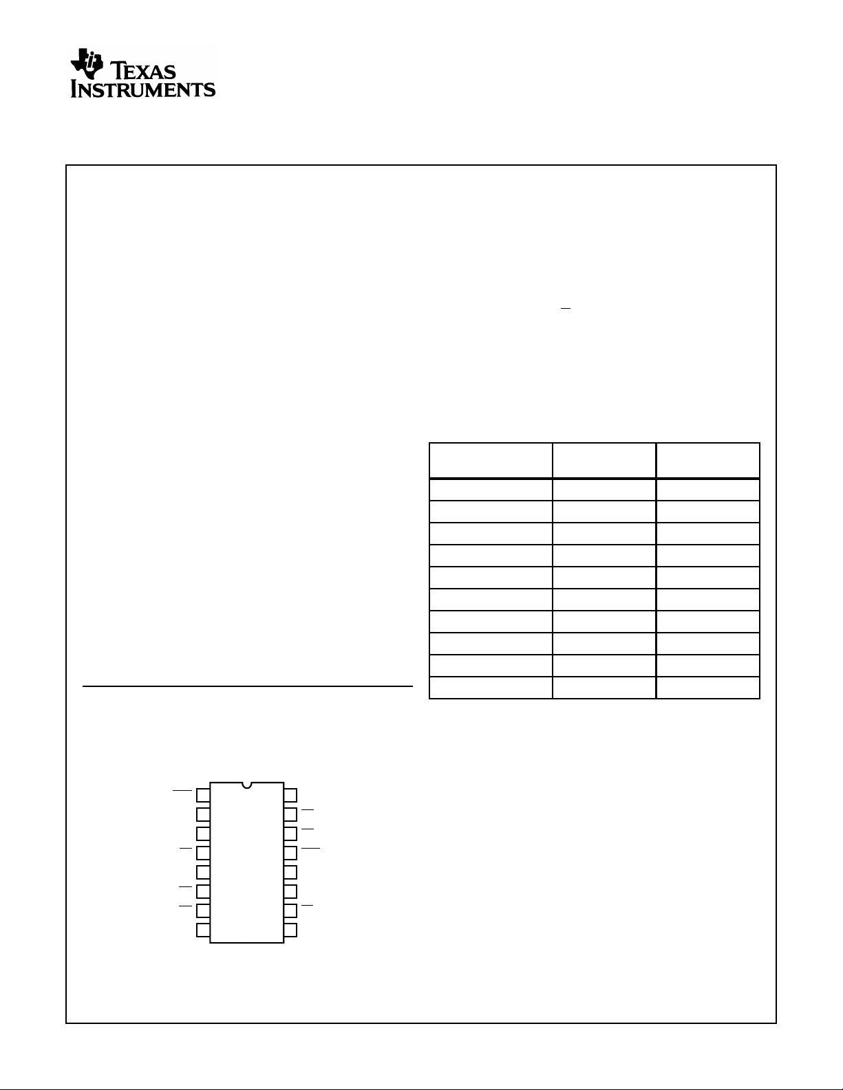
Pinout
CD54HC112, CD54HCT112 (CERDIP)
CD74HC112 (PDIP, SOIC, SOP, TSSOP)
CD74HCT112 (PDIP)
TOP VIEW
C to 125oC
CC
OH
Dual J-K Flip-Flop with Set and Reset
Negative-Edge Trigger
Description
The ’HC112 and ’HCT112 utilize silicon-gate CMOS
technology to achieveoperating speeds equivalent to LSTTL
parts. They exhibit the low power consumption of standard
CMOS integrated circuits, together with the ability to drive 10
LSTTL loads.
These flip-flops have independent J, K, Set, Reset, and
Clock inputs and Q and
negative-going transition of the clock pulse. Set and Reset
are accomplished asynchronously by low-level inputs.
The HCT logic family is functionally as well as pincompatible with the standard LS logic family.
.
Ordering Information
PART NUMBER
CD54HC112F3A -55 to 125 16 Ld CERDIP
CD54HCT112F3A -55 to 125 16 Ld CERDIP
CD74HC112E -55 to 125 16 Ld PDIP
CD74HC112MT -55 to 125 16 Ld SOIC
CD74HC112M96 -55 to 125 16 Ld SOIC
CD74HC112NSR -55 to 125 16 Ld SOP
CD74HC112PW -55 to 125 16 Ld TSSOP
CD74HC112PWR -55 to 125 16 Ld TSSOP
CD74HC112PWT -55 to 125 16 Ld TSSOP
CD74HCT112E -55 to 125 16 Ld PDIP
NOTE: When ordering, use the entire part number. The suffixes 96
and R denote tape and reel. The suffix T denotes a small-quantity
reel of 250.
Q outputs. They change state on the
TEMP. RANGE
(oC) PACKAGE
16
1
1CP
2
1K
3
1J
4
1S
5
1Q
6
1Q
7
2Q
8
GND
CAUTION: These devices are sensitive to electrostatic discharge. Users should follow proper IC Handling Procedures.
Copyright
© 2003, Texas Instruments Incorporated
V
CC
15
1R
14
2R
13
2CP
2K
12
2J
11
10
2S
9
2Q
1
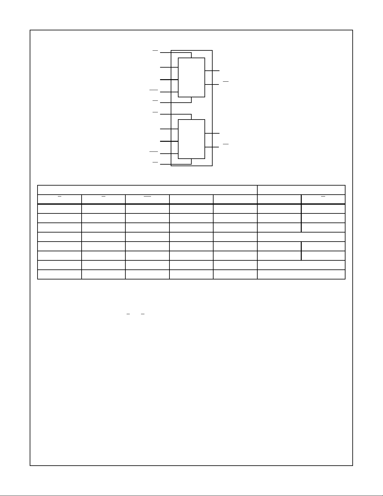
CD54HC112, CD74HC112, CD54HCT112, CD74HCT112
Functional Diagram
1S
4
1K
1CP
1R
2S
2K
2CP
2R
3
1J
2
1
15
10
11
2J
12
13
14
F/F 1
F/F 2
5
1Q
6
1Q
9
2Q
7
2Q
GND = 8
= 16
V
CC
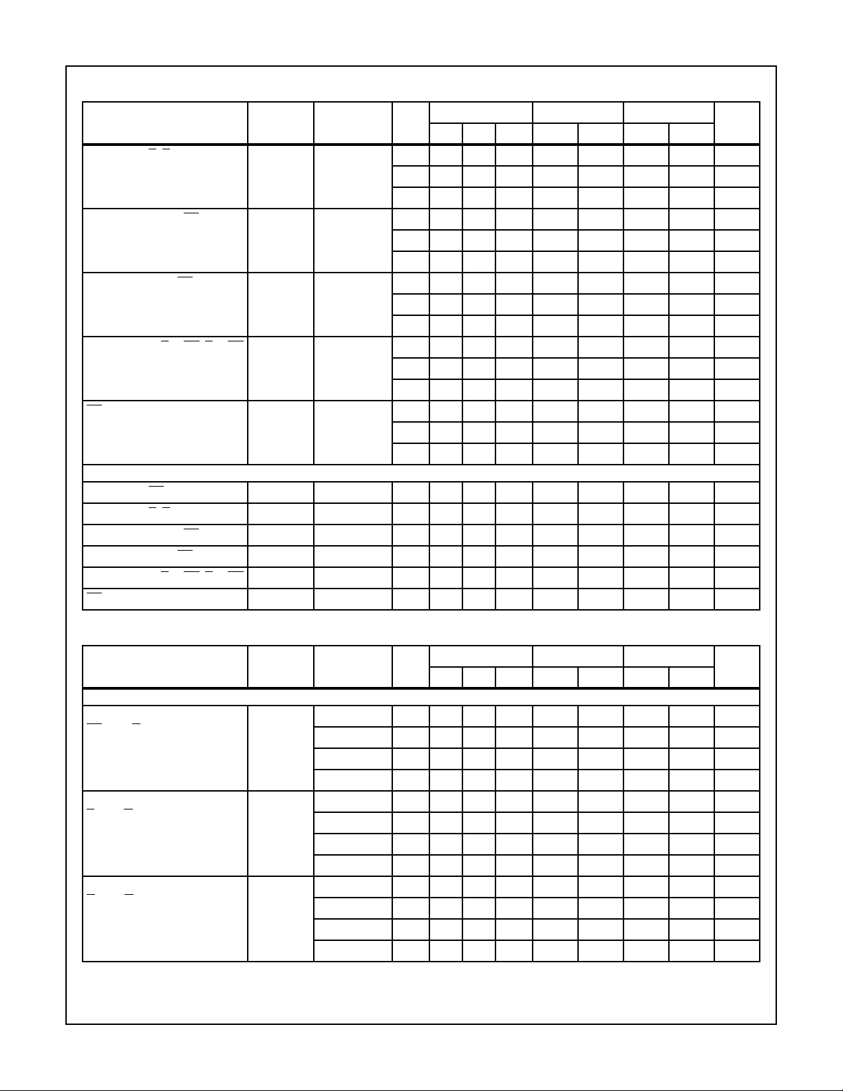
TRUTH TABLE
INPUTS OUTPUTS
S R CP J K Q Q
LHXXXHL
H
L
H
H
HH
HH
L
L
H ↓
H ↓
XXXLH
X X X H (Note 1) H (Note 1)
L L No Change
HLHL
↓
↓
LHLH
H H Toggle
H H H X X No Change
H= High Level (Steady State)
L= Low Level (Steady State)
X= Don’t Care
↓
= High-to-Low Transition
NOTE:
1. Output states unpredictable if both S and R go High simultaneously after both being low at the same time.
2
CD54HC112, CD74HC112, CD54HCT112, CD74HCT112
Absolute Maximum Ratings Thermal Information
DC Supply Voltage, VCC. . . . . . . . . . . . . . . . . . . . . . . . -0.5V to 7V
DC Input Diode Current, I
IK
For VI < -0.5V or VI > VCC + 0.5V. . . . . . . . . . . . . . . . . . . . . .±20mA
DC Drain Current, per Output, I
O
For -0.5V < VO < VCC + 0.5V. . . . . . . . . . . . . . . . . . . . . . . . . .±25mA
DC Output Diode Current, I
OK
For VO < -0.5V or VO > VCC + 0.5V . . . . . . . . . . . . . . . . . . . .±20mA
DC Output Source or Sink Current per Output Pin, I
O
For VO > -0.5V or VO < VCC + 0.5V . . . . . . . . . . . . . . . . . . . .±25mA
DC VCC or Ground Current, ICC . . . . . . . . . . . . . . . . . . . . . . . . .±50mA
Operating Conditions
Temperature Range, TA . . . . . . . . . . . . . . . . . . . . . . -55oC to 125oC
Supply Voltage Range, V
HC Types . . . . . . . . . . . . . . . . . . . . . . . . . . . . . . . . . . . . .2V to 6V
HCT Types . . . . . . . . . . . . . . . . . . . . . . . . . . . . . . . . .4.5V to 5.5V
DC Input or Output Voltage, VI, VO . . . . . . . . . . . . . . . . . 0V to V
Input Rise and Fall Time, tr, t
2V . . . . . . . . . . . . . . . . . . . . . . . . . . . . . . . . . . . . . . . 1.0ms (Max)
4.5V. . . . . . . . . . . . . . . . . . . . . . . . . . . . . . . . . . . . . . 1.0ms (Max)
6V . . . . . . . . . . . . . . . . . . . . . . . . . . . . . . . . . . . . . . . 1.0ms (Max)
CAUTION: Stresses above those listed in “Absolute Maximum Ratings” may cause permanent damage to the device. This is a stress only rating and operation
of the device at these or any other conditions above those indicated in the operational sections of this specification is not implied.
NOTE:
2. The package thermal impedance is calculated in accordance with JESD 51-7.
CC
f
Package Thermal Impedance, θJA(see Note 2):
E (PDIP) Package . . . . . . . . . . . . . . . . . . . . . . . . . . . . . . .67oC/W
NS (SOP) Package . . . . . . . . . . . . . . . . . . . . . . . . . . . . . .64oC/W
D (SOIC) Package. . . . . . . . . . . . . . . . . . . . . . . . . . . . . . .73oC/W
PW (TSSOP) Package . . . . . . . . . . . . . . . . . . . . . . . . . 108oC/W
Maximum Junction Temperature (Hermetic Package or Die) .175oC
Maximum Junction Temperature (Plastic Package) . . . . . . . . 150oC
Maximum Storage Temperature Range . . . . . . . . . .-65oC to 150oC
Maximum Lead Temperature (Soldering 10s). . . . . . . . . . . . .300oC
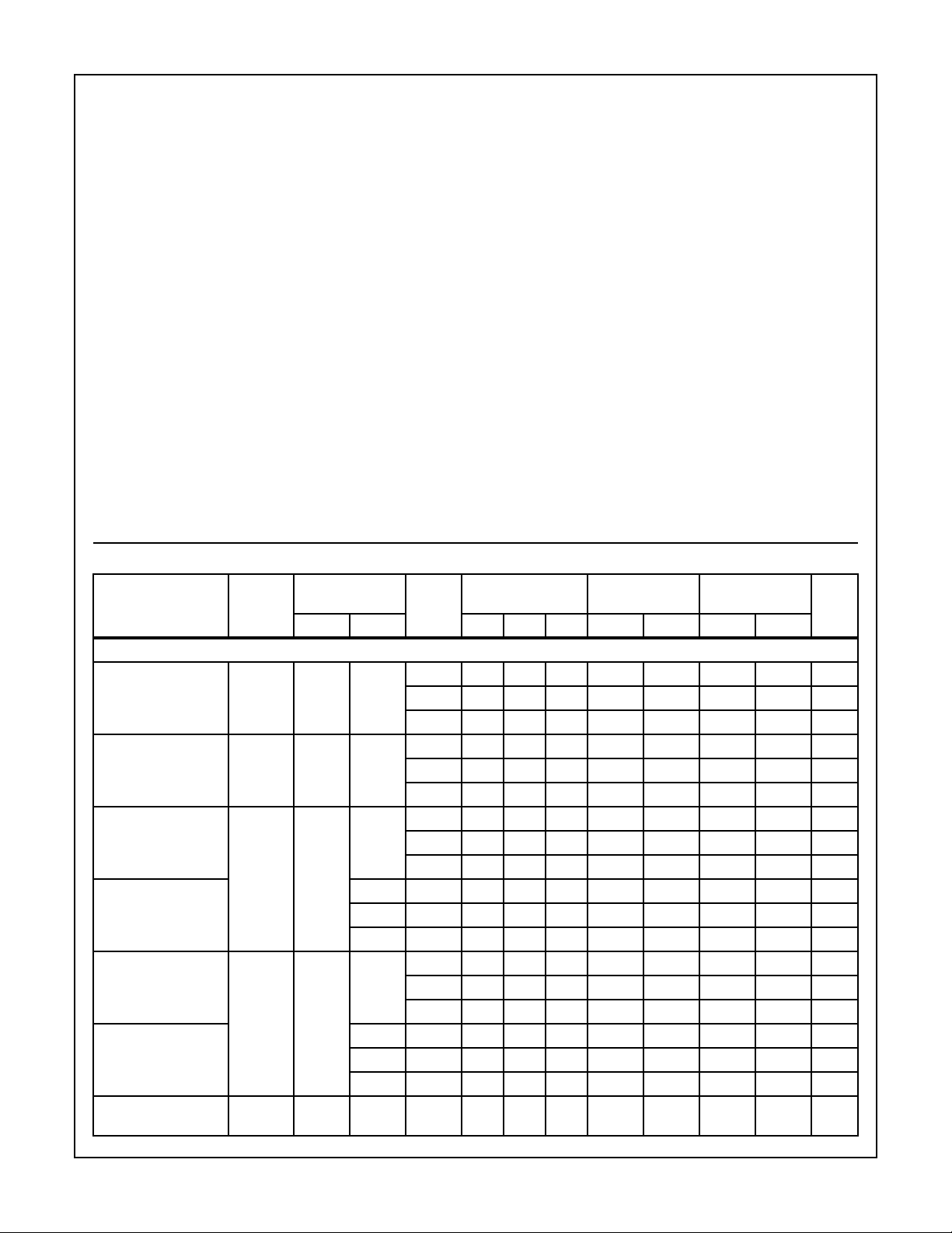
CC
DC Electrical Specifications
PARAMETER SYMBOL
HC TYPES
High Level Input
Voltage
Low Level Input
Voltage
High Level Output
Voltage
CMOS Loads
High Level Output
Voltage
TTL Loads
Low Level Output
Voltage
CMOS Loads
Low Level Output
Voltage
TTL Loads
Input Leakage
Current
V
IH
V
IL
V
OH
V
OL
I
I
TEST
CONDITIONS
25oC -40oC TO 85oC -55oC TO 125oC
VCC (V)
- - 2 1.5 - - 1.5 - 1.5 - V
4.5 3.15 - - 3.15 - 3.15 - V
6 4.2 - - 4.2 - 4.2 - V
- - 2 - - 0.5 - 0.5 - 0.5 V
4.5 - - 1.35 - 1.35 - 1.35 V
6 - - 1.8 - 1.8 - 1.8 V
VIH or
V
-0.02 2 1.9 - - 1.9 - 1.9 - V
IL
4.5 4.4 - - 4.4 - 4.4 - V
6 5.9 - - 5.9 - 5.9 - V
---------V
-4 4.5 3.98 - - 3.84 - 3.7 - V
-5.2 6 5.48 - - 5.34 - 5.2 - V
VIH or
V
0.02 2 - - 0.1 - 0.1 - 0.1 V
IL
4.5 - - 0.1 - 0.1 - 0.1 V
6 - - 0.1 - 0.1 - 0.1 V
---------V
4 4.5 - - 0.26 - 0.33 - 0.4 V
5.2 6 - - 0.26 - 0.33 - 0.4 V
VCC or
-6--±0.1 - ±1-±1 µA
GND
UNITSVI(V) IO(mA) MIN TYP MAX MIN MAX MIN MAX
3
CD54HC112, CD74HC112, CD54HCT112, CD74HCT112
DC Electrical Specifications (Continued)
TEST
CONDITIONS
PARAMETER SYMBOL
Quiescent Device
Current
I
CC
VCC or
GND
VCC (V)
0 6 - - 4 - 40 - 80 µA
HCT TYPES
High Level Input
Voltage
Low Level Input
Voltage
High Level Output
Voltage
V
IH
- - 4.5 to
5.5
V
IL
- - 4.5 to
5.5
V
OH
VIH or
V
IL
-0.02 4.5 4.4 - - 4.4 - 4.4 - V
CMOS Loads
High Level Output
-4 4.5 3.98 - - 3.84 - 3.7 - V
Voltage
TTL Loads
Low Level Output
Voltage CMOS Loads
Low Level Output
V
OL
VIH or
V
IL
0.02 4.5 - - 0.1 - 0.1 - 0.1 V
4 4.5 - - 0.26 - 0.33 - 0.4 V
Voltage
TTL Loads
Input Leakage
Current
I
I
V
CC
- 5.5 - ±0.1 - ±1-±1 µA
and
GND
Quiescent Device
Current
Additional Quiescent
Device Current Per
I
CC
∆I
CC
(Note 3)
VCC or
GND
V
CC
- 2.1
0 5.5 - - 4 - 40 - 80 µA
- 4.5 to
5.5
Input Pin: 1 Unit Load
NOTE:
3. For dual-supply systems theoretical worst case (VI = 2.4V, VCC = 5.5V) specification is 1.8mA.
25oC -40oC TO 85oC -55oC TO 125oC
2-- 2 - 2 - V
- - 0.8 - 0.8 - 0.8 V
- 100 360 - 450 - 490 µA
UNITSVI(V) IO(mA) MIN TYP MAX MIN MAX MIN MAX
HCT Input Loading Table
INPUT UNIT LOADS
1S, 2S 0.5
1K, 2K 0.6
1R, 2R 0.65
1J, 2J, 1CP, 2CP 1
NOTE: Unit Load is ∆ICClimit specified in DC Electrical Specifications table, e.g., 360µA max at 25oC.
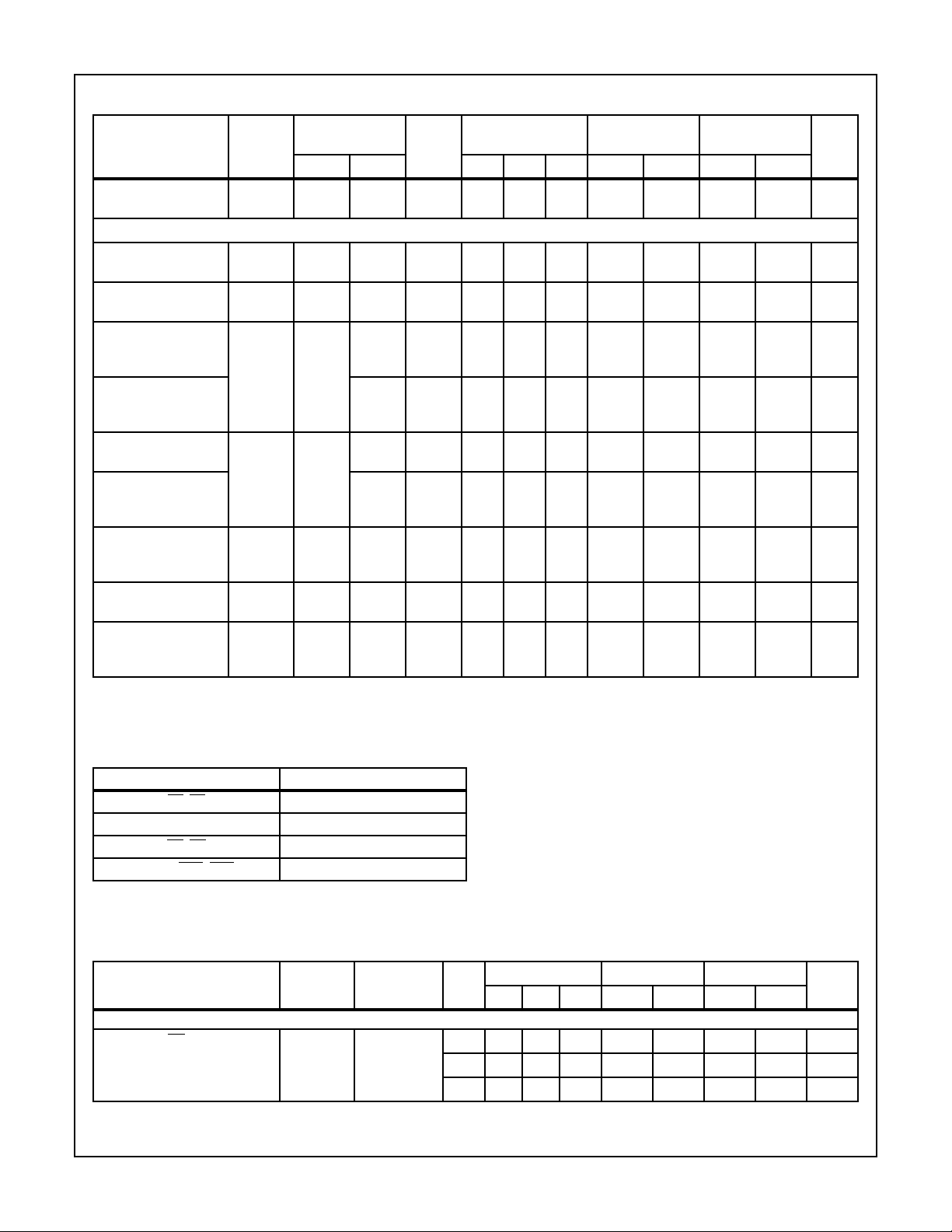
Prerequisite For Switching Specifications
TEST
PARAMETER SYMBOL
HC TYPES
Pulse Width CP t
W
CONDITIONS
- 2 80 - - 100 - 120 - ns
V
CC
(V)
25oC -40oC TO 85oC -55oC TO 125oC
UNITSMIN TYP MAX MIN MAX MIN MAX
4.5 16 - - 20 - 24 - ns
6 14 - - 17 - 20 - ns
4
CD54HC112, CD74HC112, CD54HCT112, CD74HCT112
Prerequisite For Switching Specifications (Continued)
TEST
PARAMETER SYMBOL
Pulse Width R, St
Setup Time J, K, to CP t
SU
Hold Time J, K, to CP t
Removal Time R to CP, S to CP t
CP Frequency f
REM
MAX
W
H
CONDITIONS
- 2 80 - - 100 - 120 - ns
- 2 80 - - 100 - 120 - ns
-20--0-0-ns
- 2 80 - - 100 - 120 - ns
- 2 6 - - 5 - 4 - MHz
HCT TYPES
Pulse Width CP t
Pulse Width R, St
Setup Time J, K, to CP t
Hold Time J, K, to CP t
Removal Time R to CP, S to CP t
CP Frequency f
SU
W
H
REM
W
MAX
- 4.5 16 - - 20 - 24 - ns
- 4.5 18 - - 23 - 27 - ns
- 4.5 16 - - 20 - 24 - ns
- 4.5 3 - - 3 - 3 - ns
- 4.5 20 - - 25 - 30 - ns
- 4.5 30 - - 25 - 20 - MHz
V
CC
(V)
25oC -40oC TO 85oC -55oC TO 125oC
UNITSMIN TYP MAX MIN MAX MIN MAX
4.5 16 - - 20 - 24 - ns
6 14 - - 17 - 20 - ns
4.5 16 - - 20 - 24 - ns
6 14 - - 17 - 20 - ns
4.5 0 - - 0 - 0 - ns
60--0-0-ns
4.5 16 - - 20 - 24 - ns
6 14 - - 17 - 20 - ns
4.5 30 - - 25 - 20 - MHz
6 35 - - 29 - 23 - MHz
Switching Specifications Input t
PARAMETER SYMBOL
HC TYPES
Propagation Delay,
CP to Q, Q
Propagation Delay,
S to Q, Q
Propagation Delay,
R to Q, Q
t
PLH
t
PLH
t
PLH
, tf = 6ns
r
25oC -40oC TO 85oC -55oC TO 125oC
, t
PHLCL
TEST
CONDITIONS
V
CC
(V)
= 50pF 2 - - 175 - 220 - 265 ns
CL= 50pF 4.5 - - 35 - 44 - 53 ns
CL= 15pF 5 - 14 - ----ns
CL= 50pF 6 - - 30 - 37 - 45 ns
, t
PHLCL
= 50pF 2 - - 155 - 195 - 235 ns
CL= 50pF 4.5 - - 31 - 39 - 47 ns
CL= 15pF 5 - 13 - ----ns
CL= 50pF 6 - - 26 - 33 - 40 ns
, t
PHLCL
= 50pF 2 - - 180 - 225 - 270 ns
CL= 50pF 4.5 - - 36 - 45 - 54 ns
CL= 15pF 5 - 15 - ----ns
CL= 50pF 6 - - 31 - 38 - 46 ns
UNITSMIN TYP MAX MIN MAX MIN MAX
5
I
CD54HC112, CD74HC112, CD54HCT112, CD74HCT112
Switching Specifications Input t
PARAMETER SYMBOL
Output Transition Time t
, tf = 6ns (Continued)
r
CONDITIONS
TLH
, t
THLCL
= 50pF 2 - - 75 - 95 - 110 ns
TEST
V
CC
(V)
CL= 50pF 4.5 - - 15 - 19 - 22 ns
CL= 50pF 6 - - 13 - 16 - 19 ns
Input Capacitance C
CP Frequency f
Power Dissipation Capacitance
MAX
C
I
PD
- - - - 10 - 10 - 10 pF
CL = 15pF 5 - 60 - ----MHz
- 5-12-----pF
(Notes 4, 5)
HCT TYPES
Propagation Delay,
CP to Q, Q
Propagation Delay,
S to Q, Q
Propagation Delay,
R to Q, Q
Output Transition Time t
Input Capacitance C
CP Frequency f
Power Dissipation Capacitance
t
PLH
t
PLH
t
PLH
TLH
, t
, t
, t
, t
MAX
C
PD
I
PHLCL
= 50pF 4.5 - - 35 - 44 - 53 ns
CL = 15pF 5 - 14 - ----ns
PHLCL
= 50pF 4.5 - - 32 - 40 - 48 ns
CL = 15pF 5 - 13 - ----ns
PHLCL
= 50pF 4.5 - - 37 - 46 - 56 ns
CL = 15pF 5 - 14 - ----ns
THLCL
= 50pF 4.5 - - 15 - 19 - 22 ns
- - - - 10 - 10 - 10 pF
CL = 15pF 5 - 60 - ----MHz
- 5-20-----pF
(Notes 4, 5)
NOTES:
4. CPD is used to determine the dynamic power consumption, per flip-flop.
5. PD = CPD V
2
fi + Σ CLfowhere fi = input frequency, fo = output frequency, CL = output load capacitance, VCC = supply voltage.
CC
25oC -40oC TO 85oC -55oC TO 125oC
UNITSMIN TYP MAX MIN MAX MIN MAX
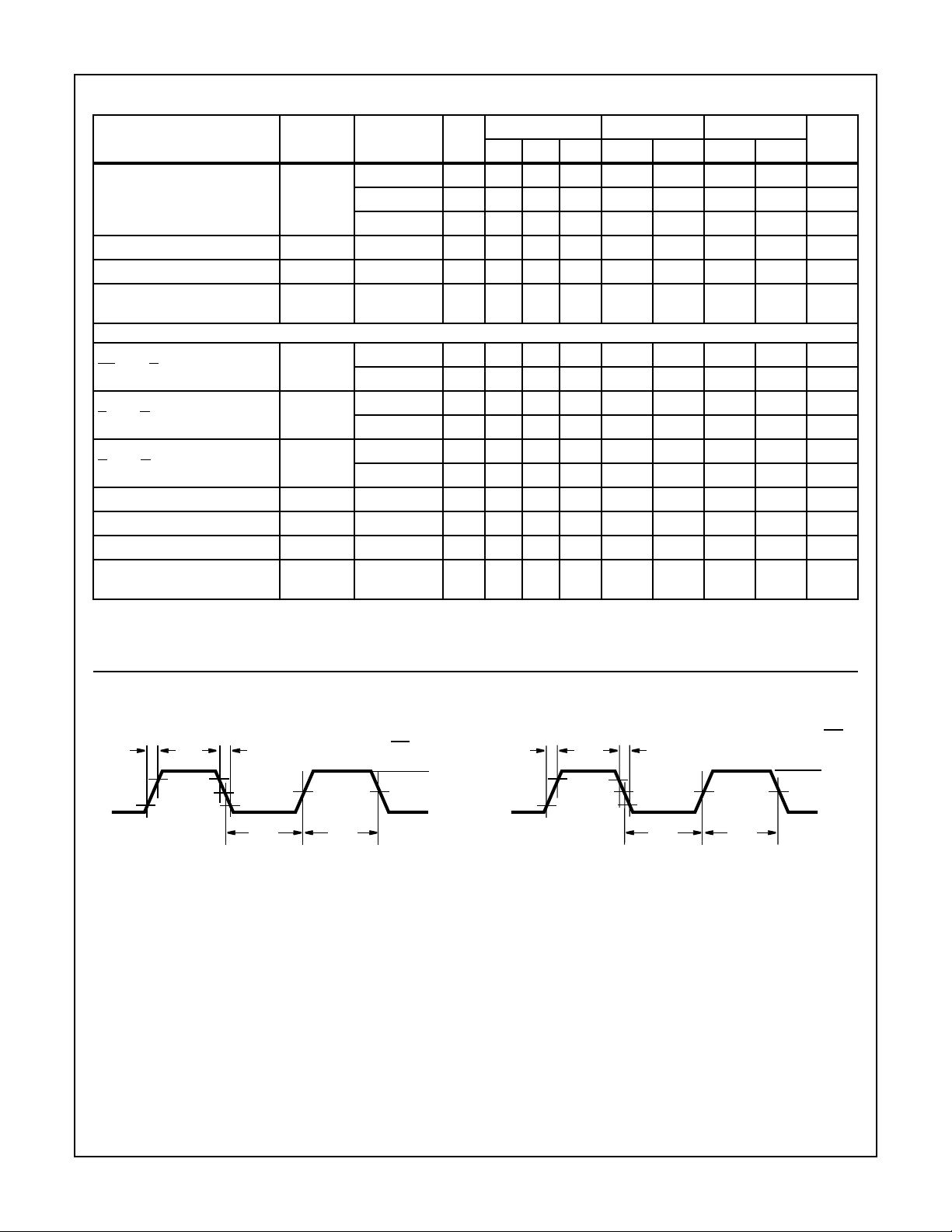
Test Circuits and Waveforms
trC
L
CLOCK
10%
90%
50%
10%
tfC
t
L
WL
tWL+ tWH=
50%
t
WH
NOTE: Outputs should be switching from 10% VCC to 90% VCC in
accordance with device truth table. For f
, input duty cycle = 50%.
MAX
FIGURE 1. HC CLOCK PULSE RISE AND FALL TIMES AND
PULSE WIDTH
f
CL
50%
I
V
CC
GND
+ tWH=
t
t
WH
WL
1.3V
fC
L
3V
GND
trCL= 6ns
CLOCK
0.3V
2.7V
1.3V
0.3V
t
t
fCL
WL
= 6ns
1.3V
NOTE: Outputs should be switching from 10% VCC to 90% VCC in
accordance with device truth table. For f
, input duty cycle = 50%.
MAX
FIGURE 2. HCT CLOCK PULSE RISE AND FALL TIMES AND
PULSE WIDTH
6
CD54HC112, CD74HC112, CD54HCT112, CD74HCT112
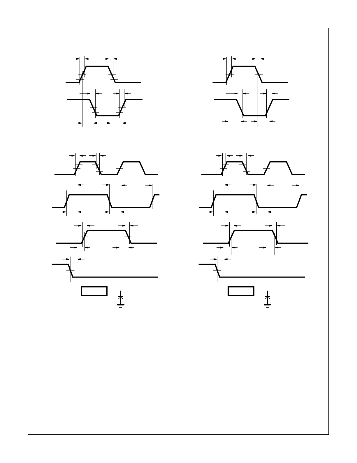
Test Circuits and Waveforms (Continued)
tr = 6ns tf = 6ns
V
INPUT
90%
50%
10%
CC
GND
tr = 6ns
INPUT
2.7V
1.3V
0.3V
= 6ns
t
f
3V
GND
t
THL
t
TLH
90%
t
50%
10%
PLH
INVERTING
OUTPUT
t
PHL
FIGURE 3. HC AND HCU TRANSITION TIMES AND PROPAGA-
TION DELAY TIMES, COMBINATION LOGIC
90%
t
PLH
t
TLH
tfC
L
V
CC
50%
GND
t
H(L)
V
CC
50%
t
SU(L)
90%
t
THL
GND
50%
10%
t
PHL
GND
CLOCK
INPUT
DAT A
INPUT
t
SU(H)
OUTPUT
t
REM
V
CC
SET, RESET
OR PRESET
trC
L
90%
10%
t
H(H)
50%
t
THL
t
TLH
90%
t
PLH
1.3V
10%
INVERTING
OUTPUT
t
PHL
FIGURE 4. HCTTRANSITION TIMES AND PROPAGATION
DELAY TIMES, COMBINATION LOGIC
CLOCK
INPUT
DAT A
INPUT
t
SU(H)
OUTPUT
t
REM
3V
SET, RESET
OR PRESET
trC
L
2.7V
0.3V
t
H(H)
1.3V
1.3V
1.3V
90%
t
PLH
1.3V
t
TLH
tfC
L
1.3V
t
H(L)
1.3V
t
SU(L)
t
THL
90%
1.3V
10%
t
PHL
3V
GND
3V
GND
GND
IC
C
L
50pF
FIGURE 5. HC SETUP TIMES, HOLD TIMES, REMOVAL TIME,
AND PROPAGATION DELAY TIMES FOR EDGE
TRIGGERED SEQUENTIAL LOGIC CIRCUITS
IC
C
L
50pF
FIGURE 6. HCTSETUPTIMES, HOLD TIMES, REMOVALTIME,
AND PROPAGATION DELAY TIMES FOR EDGE
TRIGGERED SEQUENTIAL LOGIC CIRCUITS
7
PACKAGE OPTION ADDENDUM
www.ti.com
PACKAGING INFORMATION
Orderable Device Status
5962-8970201EA ACTIVE CDIP J 16 1 TBD A42 SNPB N / A for Pkg Type
CD54HC112F3A ACTIVE CDIP J 16 1 TBD A42 SNPB N / A for Pkg Type
CD54HCT112F3A ACTIVE CDIP J 16 1 TBD A42 SNPB N / A for Pkg Type
CD74HC112E ACTIVE PDIP N 16 25 Pb-Free
CD74HC112EE4 ACTIVE PDIP N 16 25 Pb-Free
CD74HC112M96 ACTIVE SOIC D 16 2500 Green (RoHS &
CD74HC112M96E4 ACTIVE SOIC D 16 2500 Green (RoHS &
CD74HC112M96G4 ACTIVE SOIC D 16 2500 Green (RoHS &
CD74HC112MT ACTIVE SOIC D 16 250 Green (RoHS &
CD74HC112MTE4 ACTIVE SOIC D 16 250 Green (RoHS &
CD74HC112MTG4 ACTIVE SOIC D 16 250 Green (RoHS &
CD74HC112NSR ACTIVE SO NS 16 2000 Green (RoHS &
CD74HC112NSRE4 ACTIVE SO NS 16 2000 Green (RoHS &
CD74HC112NSRG4 ACTIVE SO NS 16 2000 Green (RoHS &
CD74HC112PW ACTIVE TSSOP PW 16 90 Green (RoHS &
CD74HC112PWE4 ACTIVE TSSOP PW 16 90 Green (RoHS &
CD74HC112PWG4 ACTIVE TSSOP PW 16 90 Green (RoHS &
CD74HC112PWR ACTIVE TSSOP PW 16 2000 Green (RoHS &
CD74HC112PWRE4 ACTIVE TSSOP PW 16 2000 Green (RoHS &
CD74HC112PWRG4 ACTIVE TSSOP PW 16 2000 Green (RoHS &
CD74HC112PWT ACTIVE TSSOP PW 16 250 Green (RoHS &
CD74HC112PWTE4 ACTIVE TSSOP PW 16 250 Green (RoHS &
CD74HC112PWTG4 ACTIVE TSSOP PW 16 250 Green (RoHS &
CD74HCT112E ACTIVE PDIP N 16 25 Pb-Free
CD74HCT112EE4 ACTIVE PDIP N 16 25 Pb-Free
(1)
The marketing status values are defined as follows:
(1)
Package
Type
Package
Drawing
Pins Package
Qty
Eco Plan
no Sb/Br)
no Sb/Br)
no Sb/Br)
no Sb/Br)
no Sb/Br)
no Sb/Br)
no Sb/Br)
no Sb/Br)
no Sb/Br)
no Sb/Br)
no Sb/Br)
no Sb/Br)
no Sb/Br)
no Sb/Br)
no Sb/Br)
no Sb/Br)
no Sb/Br)
no Sb/Br)
(RoHS)
(RoHS)
(RoHS)
(RoHS)
(2)
Lead/Ball Finish MSL Peak Temp
CU NIPDAU N / A for Pkg Type
CU NIPDAU N / A for Pkg Type
CU NIPDAU Level-1-260C-UNLIM
CU NIPDAU Level-1-260C-UNLIM
CU NIPDAU Level-1-260C-UNLIM
CU NIPDAU Level-1-260C-UNLIM
CU NIPDAU Level-1-260C-UNLIM
CU NIPDAU Level-1-260C-UNLIM
CU NIPDAU Level-1-260C-UNLIM
CU NIPDAU Level-1-260C-UNLIM
CU NIPDAU Level-1-260C-UNLIM
CU NIPDAU Level-1-260C-UNLIM
CU NIPDAU Level-1-260C-UNLIM
CU NIPDAU Level-1-260C-UNLIM
CU NIPDAU Level-1-260C-UNLIM
CU NIPDAU Level-1-260C-UNLIM
CU NIPDAU Level-1-260C-UNLIM
CU NIPDAU Level-1-260C-UNLIM
CU NIPDAU Level-1-260C-UNLIM
CU NIPDAU Level-1-260C-UNLIM
CU NIPDAU N / A for Pkg Type
CU NIPDAU N / A for Pkg Type
9-Oct-2007
(3)
Addendum-Page 1

PACKAGE OPTION ADDENDUM
www.ti.com
ACTIVE: Product device recommended for new designs.
LIFEBUY: TI has announced that the device will be discontinued, and a lifetime-buy period is in effect.
NRND: Not recommended for new designs. Device is in production to support existing customers, but TI does not recommend using this part in
a new design.
PREVIEW: Device has been announced but is not in production. Samples may or may not be available.
OBSOLETE: TI has discontinued the production of the device.
(2)
Eco Plan - The planned eco-friendly classification: Pb-Free (RoHS), Pb-Free (RoHS Exempt), or Green (RoHS & no Sb/Br) - please check
http://www.ti.com/productcontent for the latest availability information and additional product content details.
TBD: The Pb-Free/Green conversion plan has not been defined.
Pb-Free (RoHS): TI's terms "Lead-Free" or "Pb-Free" mean semiconductor products that are compatible with the current RoHS requirements
for all 6 substances, including the requirement that lead not exceed 0.1% by weight in homogeneous materials. Where designed to be soldered
at high temperatures, TI Pb-Free products are suitable for use in specified lead-free processes.
Pb-Free (RoHS Exempt): This component has a RoHS exemption for either 1) lead-based flip-chip solder bumps used between the die and
package, or 2) lead-based die adhesive used between the die and leadframe. The component is otherwise considered Pb-Free (RoHS
compatible) as defined above.
Green (RoHS & no Sb/Br): TI defines "Green" to mean Pb-Free (RoHS compatible), and free of Bromine (Br) and Antimony (Sb) based flame
retardants (Br or Sb do not exceed 0.1% by weight in homogeneous material)
(3)
MSL, Peak Temp. -- The Moisture Sensitivity Level rating according to the JEDEC industry standard classifications, and peak solder
temperature.
Important Information and Disclaimer:The information provided on this page represents TI's knowledge and belief as of the date that it is
provided. TI bases its knowledge and belief on information provided by third parties, and makes no representation or warranty as to the
accuracy of such information. Efforts are underway to better integrate information from third parties. TI has taken and continues to take
reasonable steps to provide representative and accurate information but may not have conducted destructive testing or chemical analysis on
incoming materials and chemicals. TI and TI suppliers consider certain information to be proprietary, and thus CAS numbers and other limited
information may not be available for release.
9-Oct-2007
In no event shall TI's liability arising out of such information exceed the total purchase price of the TI part(s) at issue in this document sold by TI
to Customer on an annual basis.
Addendum-Page 2

PACKAGE MATERIALS INFORMATION
www.ti.com
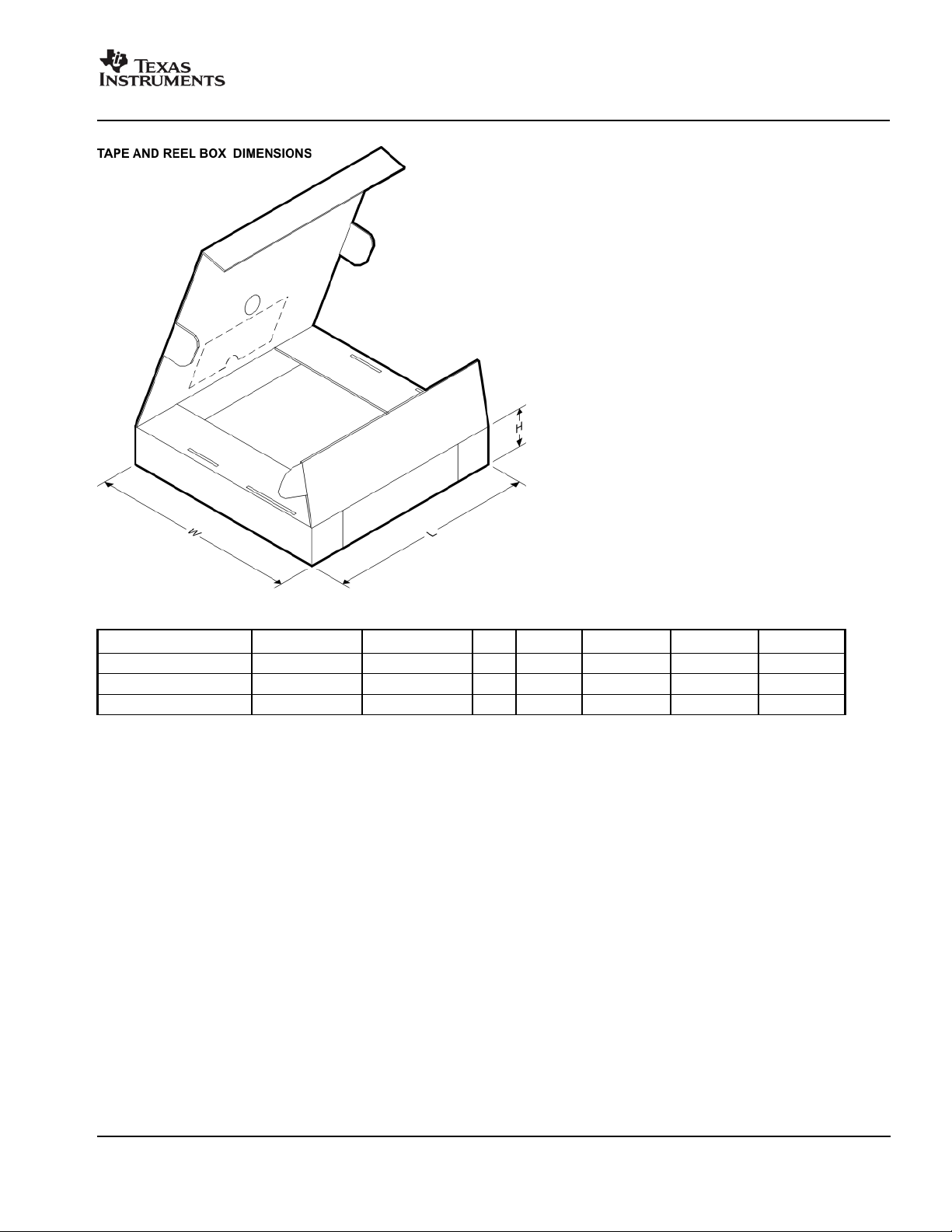
TAPE AND REEL INFORMATION
19-Mar-2008
*All dimensions are nominal
Device Package
Type
CD74HC112M96 SOIC D 16 2500 330.0 16.4 6.5 10.3 2.1 8.0 16.0 Q1
CD74HC112NSR SO NS 16 2000 330.0 16.4 8.2 10.5 2.5 12.0 16.0 Q1
CD74HC112PWR TSSOP PW 16 2000 330.0 12.4 7.0 5.6 1.6 8.0 12.0 Q1
Package
Drawing
Pins SPQ Reel
Diameter
(mm)
Reel
Width
W1 (mm)
A0 (mm) B0 (mm) K0 (mm) P1
(mm)W(mm)
Pin1
Quadrant
Pack Materials-Page 1
PACKAGE MATERIALS INFORMATION
www.ti.com
19-Mar-2008
*All dimensions are nominal
Device Package Type Package Drawing Pins SPQ Length (mm) Width (mm) Height (mm)
CD74HC112M96 SOIC D 16 2500 333.2 345.9 28.6
CD74HC112NSR SO NS 16 2000 346.0 346.0 33.0
CD74HC112PWR TSSOP PW 16 2000 346.0 346.0 29.0
Pack Materials-Page 2


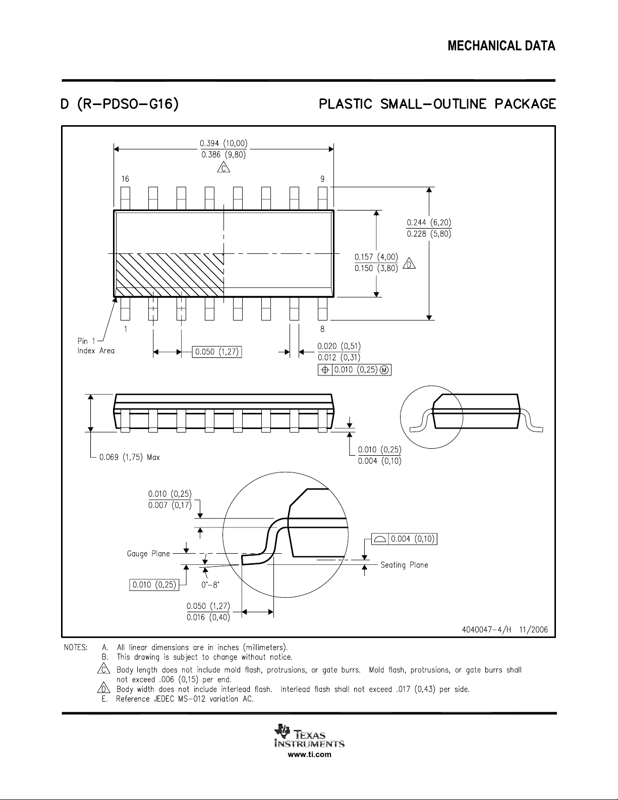
MECHANICAL DATA
MTSS001C – JANUARY 1995 – REVISED FEBRUARY 1999
PW (R-PDSO-G**) PLASTIC SMALL-OUTLINE PACKAGE
14 PINS SHOWN
0,65
1,20 MAX
14
0,30
0,19
8
4,50
4,30
PINS **
7
Seating Plane
0,15
0,05
8
1
A
DIM
14
0,10
6,60
6,20
M
0,10
0,15 NOM
0°–8°
2016
Gage Plane
24
0,25
0,75
0,50
28
A MAX
A MIN
NOTES: A. All linear dimensions are in millimeters.
B. This drawing is subject to change without notice.
C. Body dimensions do not include mold flash or protrusion not to exceed 0,15.
D. Falls within JEDEC MO-153
3,10
2,90
5,10
4,90
5,10
4,90
6,60
6,40
7,90
7,70
9,80
9,60
4040064/F 01/97
POST OFFICE BOX 655303 • DALLAS, TEXAS 75265


IMPORTANT NOTICE
Texas Instruments Incorporated and its subsidiaries (TI) reserve the right to make corrections, modifications, enhancements, improvements,
and other changes to its products and services at any time and to discontinue any product or service without notice. Customers should
obtain the latest relevant information before placing orders and should verify that such information is current and complete. All products are
sold subject to TI’s terms and conditions of sale supplied at the time of order acknowledgment.
TI warrants performance of its hardware products to the specifications applicable at the time of sale in accordance with TI’s standard
warranty. Testing and other quality control techniques are used to the extent TI deems necessary to support this warranty. Except where
mandated by government requirements, testing of all parameters of each product is not necessarily performed.
TI assumes no liability for applications assistance or customer product design. Customers are responsible for their products and
applications using TI components. To minimize the risks associated with customer products and applications, customers should provide
adequate design and operating safeguards.
TI does not warrant or represent that any license, either express or implied, is granted under any TI patent right, copyright, mask work right,
or other TI intellectual property right relating to any combination, machine, or process in which TI products or services are used. Information
published by TI regarding third-party products or services does not constitute a license from TI to use such products or services or a
warranty or endorsement thereof. Use of such information may require a license from a third party under the patents or other intellectual
property of the third party, or a license from TI under the patents or other intellectual property of TI.
Reproduction of TI information in TI data books or data sheets is permissible only if reproduction is without alteration and is accompanied
by all associated warranties, conditions, limitations, and notices. Reproduction of this information with alteration is an unfair and deceptive
business practice. TI is not responsible or liable for such altered documentation. Information of third parties may be subject to additional
restrictions.
Resale of TI products or services with statements different from or beyond the parameters stated by TI for that product or service voids all
express and any implied warranties for the associated TI product or service and is an unfair and deceptive business practice. TI is not
responsible or liable for any such statements.
TI products are not authorized for use in safety-critical applications (such as life support) where a failure of the TI product would reasonably
be expected to cause severe personal injury or death, unless officers of the parties have executed an agreement specifically governing
such use. Buyers represent that they have all necessary expertise in the safety and regulatory ramifications of their applications, and
acknowledge and agree that they are solely responsible for all legal, regulatory and safety-related requirements concerning their products
and any use of TI products in such safety-critical applications, notwithstanding any applications-related information or support that may be
provided by TI. Further, Buyers must fully indemnify TI and its representatives against any damages arising out of the use of TI products in
such safety-critical applications.
TI products are neither designed nor intended for use in military/aerospace applications or environments unless the TI products are
specifically designated by TI as military-grade or "enhanced plastic." Only products designated by TI as military-grade meet military
specifications. Buyers acknowledge and agree that any such use of TI products which TI has not designated as military-grade is solely at
the Buyer's risk, and that they are solely responsible for compliance with all legal and regulatory requirements in connection with such use.
TI products are neither designed nor intended for use in automotive applications or environments unless the specific TI products are
designated by TI as compliant with ISO/TS 16949 requirements. Buyers acknowledge and agree that, if they use any non-designated
products in automotive applications, TI will not be responsible for any failure to meet such requirements.
Following are URLs where you can obtain information on other Texas Instruments products and application solutions:
Products Applications
Amplifiers amplifier.ti.com Audio www.ti.com/audio
Data Converters dataconverter.ti.com Automotive www.ti.com/automotive
DSP dsp.ti.com Broadband www.ti.com/broadband
Clocks and Timers www.ti.com/clocks Digital Control www.ti.com/digitalcontrol
Interface interface.ti.com Medical www.ti.com/medical
Logic logic.ti.com Military www.ti.com/military
Power Mgmt power.ti.com Optical Networking www.ti.com/opticalnetwork
Microcontrollers microcontroller.ti.com Security www.ti.com/security
RFID www.ti-rfid.com Telephony www.ti.com/telephony
RF/IF and ZigBee® Solutions www.ti.com/lprf Video & Imaging www.ti.com/video
Mailing Address: Texas Instruments, Post Office Box 655303, Dallas, Texas 75265
Copyright © 2008, Texas Instruments Incorporated
Wireless www.ti.com/wireless
 Loading...