

55°C to 125°C
SOIC
M
ACT138M
查询CD54ACT138F3A供应商
CD54ACT138, CD74ACT138
3-LINE TO 8-LINE DECODERS/DEMULTIPLEXERS
SCHS329A – JANUARY 2003 – REVISED FEBRUARY 2003
D
Inputs Are TTL-Voltage Compatible
D
Speed of Bipolar F, AS, and S, With
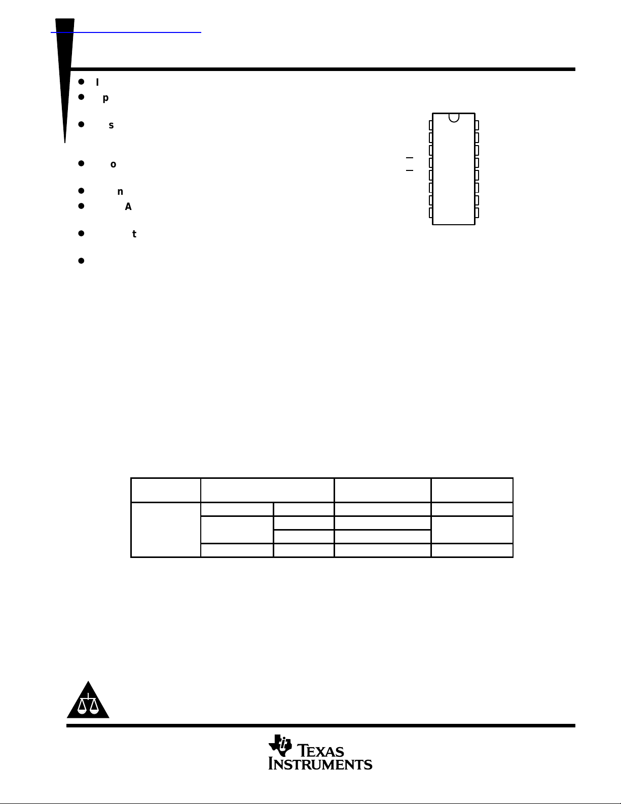
CD54ACT138 ...F PACKAGE
CD74ACT138 ...E OR M PACKAGE
(TOP VIEW)
Significantly Reduced Power Consumption
D
Designed Specifically for High-Speed
Memory Decoders and Data-Transmission
Systems
D
Incorporate Three Enable Inputs to Simplify
Cascading and/or Data Reception
D
Balanced Propagation Delays
D
±24-mA Output Drive Current
– Fanout to 15 F Devices
D
SCR-Latchup-Resistant CMOS Process and
G
2A
G
2B
G1
Y7
GND
1
A
2
B
3
C
4
5
6
7
8
16
15
14
13
12
11
10
V
CC
Y0
Y1
Y2
Y3
Y4
Y5
9
Y6
Circuit Design
D
Exceeds 2-kV ESD Protection Per
MIL-STD-883, Method 3015
description/ordering information
The ’ACT138 decoders/demultiplexers are designed for high-performance memory-decoding and data-routing
applications that require very short propagation-delay times. In high-performance memory systems, these
decoders can be used to minimize the effects of system decoding. When employed with high-speed memories
utilizing a fast enable circuit, the delay times of these decoders and the enable time of the memory usually are
less than the typical access time of the memory . This means that the effective system delay introduced by the
decoders is neg ligible.
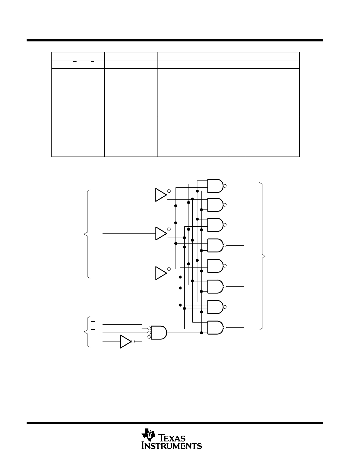
The conditions at the binary-select inputs and the three enable inputs select one of eight output lines. Two
active-low and one active-high enable inputs reduce the need for external gates or inverters when expanding.
A 24-line decoder can be implemented without external inverters, and a 32-line decoder requires only one
inverter. An enable input can be used as a data input for demultiplexing applications (see Application
Information).
ORDERING INFORMATION
T
A
PDIP – E Tube CD74ACT138E CD74ACT138E
°
–
†
Package drawings, standard packing quantities, thermal data, symbolization, and PCB design guidelines
are available at www.ti.com/sc/package.
°
CDIP – F Tube CD54ACT138F3A CD54ACT138F3A
PACKAGE
–
†
Tube CD74ACT138M
Tape and reel CD74ACT138M96
ORDERABLE
PART NUMBER
TOP-SIDE
MARKING
Please be aware that an important notice concerning availability, standard warranty, and use in critical applications of
Texas Instruments semiconductor products and disclaimers thereto appears at the end of this data sheet.
PRODUCTION DATA information is current as of publication date.
Products conform to specifications per the terms of Texas Instruments
standard warranty. Production processing does not necessarily include
testing of all parameters.
POST OFFICE BOX 655303 • DALLAS, TEXAS 75265
Copyright 2003, Texas Instruments Incorporated
On products compliant to MIL-PRF-38535, all parameters are tested
unless otherwise noted. On all other products, production
processing does not necessarily include testing of all parameters.
1
CD54ACT138, CD74ACT138
3-LINE TO 8-LINE DECODERS/DEMULTIPLEXERS
SCHS329A – JANUARY 2003 – REVISED FEBRUARY 2003
FUNCTION TABLE
ENABLE INPUTS SELECT INPUTS OUTPUTS
G1 G2A G2B C B A Y0 Y1 Y2 Y3 Y4 Y5 Y6 Y7
X H X X X X H H H H H H H H
X XHXXXHHHHHHHH
L XXXXXHHHHHHHH
H LLLLLLHHHHHHH
H LLLLHHLHHHHHH
H LLLHLHHLHHHHH
H LLLHHHHHLHHHH
H LLHLLHHHHLHHH
H LLHLHHHHHHLHH
H LLHHLHHHHHHLH
H L L H H H H H H H H H H L
logic diagram (positive logic)
1
A
15
14
Y0
Y1
Select
Inputs
Enable
Inputs
13
12
11
10
Y2
Y3
Data
Y4
Y5
9
Y6
7
Y7
Outputs
2
B
3
C
4
2A
G
5
G
2B
6
G1
2
POST OFFICE BOX 655303 • DALLAS, TEXAS 75265
CD54ACT138, CD74ACT138
3-LINE TO 8-LINE DECODERS/DEMULTIPLEXERS
SCHS329A – JANUARY 2003 – REVISED FEBRUARY 2003
absolute maximum ratings over operating free-air temperature range (unless otherwise noted)
Supply voltage range, V
Input clamp current, I
Output clamp current, I
Continuous output current, I
Continuous current through V
Package thermal impedance, θ
–0.5 V to 6 V. . . . . . . . . . . . . . . . . . . . . . . . . . . . . . . . . . . . . . . . . . . . . . . . . . . . . . . . . .
CC
(VI < 0 V or VI > VCC) (see Note 1) ±20 mA. . . . . . . . . . . . . . . . . . . . . . . . . . . . . . . . . . .
IK
(VO < 0 V or VO > VCC) (see Note 1) ±50 mA. . . . . . . . . . . . . . . . . . . . . . . . . . . . . .
OK
(VO > 0 V or VO < VCC) ±50 mA. . . . . . . . . . . . . . . . . . . . . . . . . . . . . . . . . . . . . . .
O
or GND ±100 mA. . . . . . . . . . . . . . . . . . . . . . . . . . . . . . . . . . . . . . . . . . . . . . . . . .
CC
(see Note 2): E package 67°C/W. . . . . . . . . . . . . . . . . . . . . . . . . . . . . . . . . . .
JA
†
M package 73°C/W. . . . . . . . . . . . . . . . . . . . . . . . . . . . . . . . . .
Storage temperature range, T
†
Stresses beyond those listed under “absolute maximum ratings” may cause permanent damage to the device. These are stress ratings only, and
functional operation of the device at these or any other conditions beyond those indicated under “recommended operating conditions” is not
implied. Exposure to absolute-maximum-rated conditions for extended periods may affect device reliability.
NOTES: 1. The input and output voltage ratings may be exceeded if the input and output current ratings are observed.
2. The package thermal impedance is calculated in accordance with JESD 51-7.
–65°C to 150°C. . . . . . . . . . . . . . . . . . . . . . . . . . . . . . . . . . . . . . . . . . . . . . . . . . .
stg
recommended operating conditions (see Note 3)
CC
CC
–55°C to
125°C
0 V
0 V
TA = 25°C
MIN MAX MIN MAX MIN MAX
V
V
V
V
V
I
OH
I
OL
∆t/∆v Input transition rise or fall rate 10 10 10 ns/V
NOTE 3: All unused inputs of the device must be held at VCC or GND to ensure proper device operation. Refer to the TI application report,
Supply voltage 4.5 5.5 4.5 5.5 4.5 5.5 V
CC
High-level input voltage 2 2 2 V
IH
Low-level input voltage 0.8 0.8 0.8 V
IL
Input voltage 0 V
I
Output voltage 0 V
O
High-level output current –24 –24 –24 mA
Low-level output current 24 24 24 mA
Implications of Slow or Floating CMOS Inputs, literature number SCBA004.
CC
CC
–40°C to
85°C
0 V
0 V
CC
CC
UNIT
V
V
POST OFFICE BOX 655303 • DALLAS, TEXAS 75265
3
CD54ACT138, CD74ACT138
CC
V
V
V
or V
V
V
V
V
or V
V
(INPUT)
(OUTPUT)
A, B, C
Any Y
ns
G1
Any Y
ns
G2A, G2B
Any Y
ns
3-LINE TO 8-LINE DECODERS/DEMULTIPLEXERS
SCHS329A – JANUARY 2003 – REVISED FEBRUARY 2003
electrical characteristics over recommended operating free-air temperature range (unless
otherwise noted)
PARAMETER TEST CONDITIONS V
IOH = –50 µA 4.5 V 4.4 4.4 4.4
=
OH
OL
I
I
I
CC
‡
D
I
CC
C
†
‡
i
T est one output at a time, not exceeding 1-second duration. Measurement is made by forcing indicated current and measuring voltage to minimize
power dissipation. T est verifies a minimum 50-Ω transmission-line drive capability at 85°C and 75-Ω transmission-line drive capability at 125°C.
Additional quiescent supply current per input pin, TTL inputs high, 1 unit load
I
IH
IL
=
I
IH
IL
VI = VCC or GND 5.5 V ±0.1 ±1 ±1 µA
VI = VCC or GND, IO = 0 5.5 V 8 160 80 µA
VI = VCC – 2.1 V
IOH = –24 mA 4.5 V 3.94 3.7 3.8
IOH = –50 mA
IOH = –75 mA
IOL = 50 µA 4.5 V 0.1 0.1 0.1
IOL = 24 mA 4.5 V 0.36 0.5 0.44
IOL = 50 mA
IOL = 75 mA
†
5.5 V 3.85
†
5.5 V 3.85
†
†
5.5 V 1.65
5.5 V 1.65
4.5 V to
5.5 V
TA = 25°C
MIN MAX MIN MAX MIN MAX
–55°C to
125°C
2.4 3 2.8 mA
10 10 10 pF
–40°C to
85°C
UNIT
ACT INPUT LOAD TABLE
INPUT
A, B, or C 0.83
G2A or G2B
G1 0.42
Unit Load is ∆ICC limit specified in
electrical characteristics table
(e.g., 2.4 mA at 25°C).
UNIT LOAD
1
switching characteristics over recommended operating free-air temperature range,
= 5 V ± 0.5 V, CL = 50 pF (unless otherwise noted) (see Figure 1)
V
CC
PARAMETER
t
PLH
t
PHL
t
PLH
t
PHL
t
PLH
t
PHL
FROM
TO
–55°C to
125°C
MIN MAX MIN MAX
3 12 3.1 10.9
3 12 3.1 10.9
2.8 11 2.8 10
2.8 11 2.8 10
2.6 10.5 2.7 9.5
2.6 10.5 2.7 9.5
–40°C to
operating characteristics, VCC = 5 V, TA = 25°C
PARAMETER TYP UNIT
C
pd
Power dissipation capacitance 110 pF
85°C
UNIT
4
POST OFFICE BOX 655303 • DALLAS, TEXAS 75265

CD54ACT138, CD74ACT138
3-LINE TO 8-LINE DECODERS/DEMULTIPLEXERS
SCHS329A – JANUARY 2003 – REVISED FEBRUARY 2003
PARAMETER MEASUREMENT INFORMATION
CC
1.5 V
t
S1
t
rec
t
PHL
PLH
50%
From Output
Under Test
CL = 50 pF
(see Note A)
CLR
Input
CLK
VOLTAGE WAVEFORMS
RECOVERY TIME
Input
In-Phase
Output
Out-of-Phase
Output
PROPAGATION DELAY AND OUTPUT TRANSITION TIMES
1.5 V 1.5 V
t
PLH
50%
t
PHL
VOLTAGE WAVEFORMS
R1 = 500 Ω Open
R2 = 500 Ω
LOAD CIRCUIT
1.5 V
90% 90%
t
r
50% V
10% 10%
t
f
2 × V
GND
CC
3 V
0 V
3 V
0 V
50% V
10%10%
90%90%
TEST S1
t
w
1.5 V
Open
2 × V
GND
t
20% V
80% V
CC
3 V
0 V
3 V
0 V
h
3 V
1.5 V
10%10%
0 V
t
f
3 V
0 V
t
PLZ
≈V
PHZ
CC
CC
V
OL
V
OH
≈0 V
CC
CC
CC
20% V
t
80% V
t
PLH/tPHL
t
PLZ/tPZL
t
PHZ/tPZH
Input
Reference
Input
Data
1.5 V
Input
SETUP AND HOLD AND INPUT RISE AND FALL TIMES
3 V
0 V
V
OH
CC
V
OL
t
f
V
OH
V
OL
t
r
Output
Control
Output
Waveform 1
S1 at 2 × V
(see Note B)
Output
Waveform 2
S1 at GND
(see Note B)
OUTPUT ENABLE AND DISABLE TIMES
CC
1.5 V 1.5 V
VOLTAGE WAVEFORMS
PULSE DURATION
t
su
90% 90%
t
r
VOLTAGE WAVEFORMS
1.5 V 1.5 V
t
PZL
t
PZH
VOLTAGE WAVEFORMS
NOTES: A. CL includes probe and test-fixture capacitance.
B. Waveform 1 is for an output with internal conditions such that the output is low except when disabled by the output control.
Waveform 2 is for an output with internal conditions such that the output is high except when disabled by the output control.
C. All input pulses are supplied by generators having the following characteristics: PRR ≤ 1 MHz, ZO = 50 Ω, tr = 3 ns, tf = 3 ns.
Phase relationships between waveforms are arbitrary.
D. For clock inputs, f
E. The outputs are measured one at a time with one input transition per measurement.
F. t
G. t
H. t
and t
PLH
PZL
PLZ
I. All parameters and waveforms are not applicable to all devices.
and t
and t
PHL
PZH
PHZ
is measured with the input duty cycle at 50%.
max
are the same as tpd.
are the same as ten.
are the same as t
dis
.
Figure 1. Load Circuit and Voltage Waveforms
POST OFFICE BOX 655303 • DALLAS, TEXAS 75265
5

CD54ACT138, CD74ACT138
3-LINE TO 8-LINE DECODERS/DEMULTIPLEXERS
SCHS329A – JANUARY 2003 – REVISED FEBRUARY 2003
APPLICATION INFORMATION
V
CC
A0
A1
A2
A3
A4
CD74ACT138
1
2
3
6
4
5
1
2
3
6
4
5
BIN/OCT
1
2
4
&
EN
CD74ACT138
BIN/OCT
1
2
4
&
EN
0
1
2
3
4
5
6
7
0
1
2
3
4
5
6
7
15
14
13
12
11
10
15
14
13
12
11
10
0
1
2
3
4
5
9
6
7
7
8
9
10
11
12
13
9
14
7
15
CD74ACT138
1
2
3
6
4
5
BIN/OCT
1
2
4
&
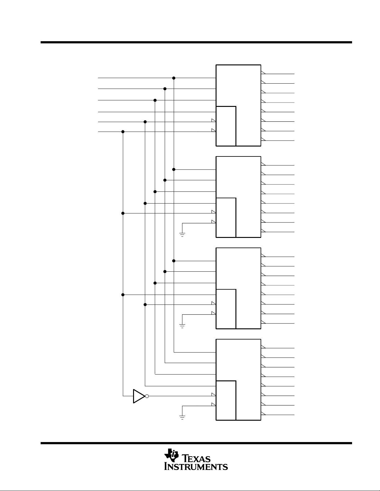
Figure 2. 24-Bit Decoding Scheme
EN
15
0
1
2
3
4
5
6
7
14
13
12
11
10
16
17
18
19
20
21
9
22
7
23
6
POST OFFICE BOX 655303 • DALLAS, TEXAS 75265
CD54ACT138, CD74ACT138
3-LINE TO 8-LINE DECODERS/DEMULTIPLEXERS
SCHS329A – JANUARY 2003 – REVISED FEBRUARY 2003
APPLICATION INFORMATION
CD74ACT138
A0
A1
A2
V
CC
A3
A4
1
2
3
6
4
5
1
2
3
6
4
5
BIN/OCT
1
2
4
&
EN
CD74ACT138
BIN/OCT
1
2
4
&
EN
0
1
2
3
4
5
6
7
0
1
2
3
4
5
6
7
15
14
13
12
11
10
15
14
13
12
11
10
0
1
2
3
4
5
9
6
7
7
8
9
10
11
12
13
9
14
7
15
CD74ACT138
1
2
3
6
4
5
1
2
3
6
4
5
BIN/OCT
1
2
4
&
EN
CD74ACT138
BIN/OCT
1
2
4
&
EN
0
1
2
3
4
5
6
7
0
1
2
3
4
5
6
7
15
14
13
12
11
10
15
14
13
12
11
10
16
17
18
19
20
21
9
22
7
23
24
25
26
27
28
29
9
30
7
31
Figure 3. 32-Bit Decoding Scheme
POST OFFICE BOX 655303 • DALLAS, TEXAS 75265
7


IMPORTANT NOTICE
Texas Instruments Incorporated and its subsidiaries (TI) reserve the right to make corrections, modifications,
enhancements, improvements, and other changes to its products and services at any time and to discontinue
any product or service without notice. Customers should obtain the latest relevant information before placing
orders and should verify that such information is current and complete. All products are sold subject to TI’s terms
and conditions of sale supplied at the time of order acknowledgment.
TI warrants performance of its hardware products to the specifications applicable at the time of sale in
accordance with TI’s standard warranty. Testing and other quality control techniques are used to the extent TI
deems necessary to support this warranty . Except where mandated by government requirements, testing of all
parameters of each product is not necessarily performed.
TI assumes no liability for applications assistance or customer product design. Customers are responsible for
their products and applications using TI components. To minimize the risks associated with customer products
and applications, customers should provide adequate design and operating safeguards.
TI does not warrant or represent that any license, either express or implied, is granted under any TI patent right,
copyright, mask work right, or other TI intellectual property right relating to any combination, machine, or process
in which TI products or services are used. Information published by TI regarding third-party products or services
does not constitute a license from TI to use such products or services or a warranty or endorsement thereof.
Use of such information may require a license from a third party under the patents or other intellectual property
of the third party, or a license from TI under the patents or other intellectual property of TI.
Reproduction of information in TI data books or data sheets is permissible only if reproduction is without
alteration and is accompanied by all associated warranties, conditions, limitations, and notices. Reproduction
of this information with alteration is an unfair and deceptive business practice. TI is not responsible or liable for
such altered documentation.
Resale of TI products or services with statements different from or beyond the parameters stated by TI for that
product or service voids all express and any implied warranties for the associated TI product or service and
is an unfair and deceptive business practice. TI is not responsible or liable for any such statements.
Following are URLs where you can obtain information on other Texas Instruments products and application
solutions:
Products Applications
Amplifiers amplifier.ti.com Audio www.ti.com/audio
Data Converters dataconverter.ti.com Automotive www.ti.com/automotive
DSP dsp.ti.com Broadband www.ti.com/broadband
Interface interface.ti.com Digital Control www.ti.com/digitalcontrol
Logic logic.ti.com Military www.ti.com/military
Power Mgmt power.ti.com Optical Networking www.ti.com/opticalnetwork
Microcontrollers microcontroller.ti.com Security www.ti.com/security
Telephony www.ti.com/telephony
Video & Imaging www.ti.com/video
Wireless www.ti.com/wireless
Mailing Address: Texas Instruments
Post Office Box 655303 Dallas, Texas 75265
Copyright 2004, Texas Instruments Incorporated
 Loading...