

Page 1
CD54AC273, CD74AC273
Data sheet acquired from Harris Semiconductor
SCHS249B
CD54ACT273, CD74ACT273
August 1998 - Revised July 2002
Features
• Buffered Inputs
• Typical Propagation Delay
- 6.5ns at V
= 5V, TA = 25oC, CL = 50pF
CC
• Exceeds 2kV ESD Protection MIL-STD-883, Method
3015
• SCR-Latchup-Resistant CMOS Process and Circuit
Design
• Speed of Bipolar FAST™/AS/S with Significantly
Reduced Power Consumption
• Balanced Propagation Delays
• AC Types Feature 1.5V to 5.5V Operation and
Balanced Noise Immunity at 30% of the Supply
• ±24mA Output Drive Current
- Fanout to 15 FAST™ ICs
- Drives 50Ω Transmission Lines
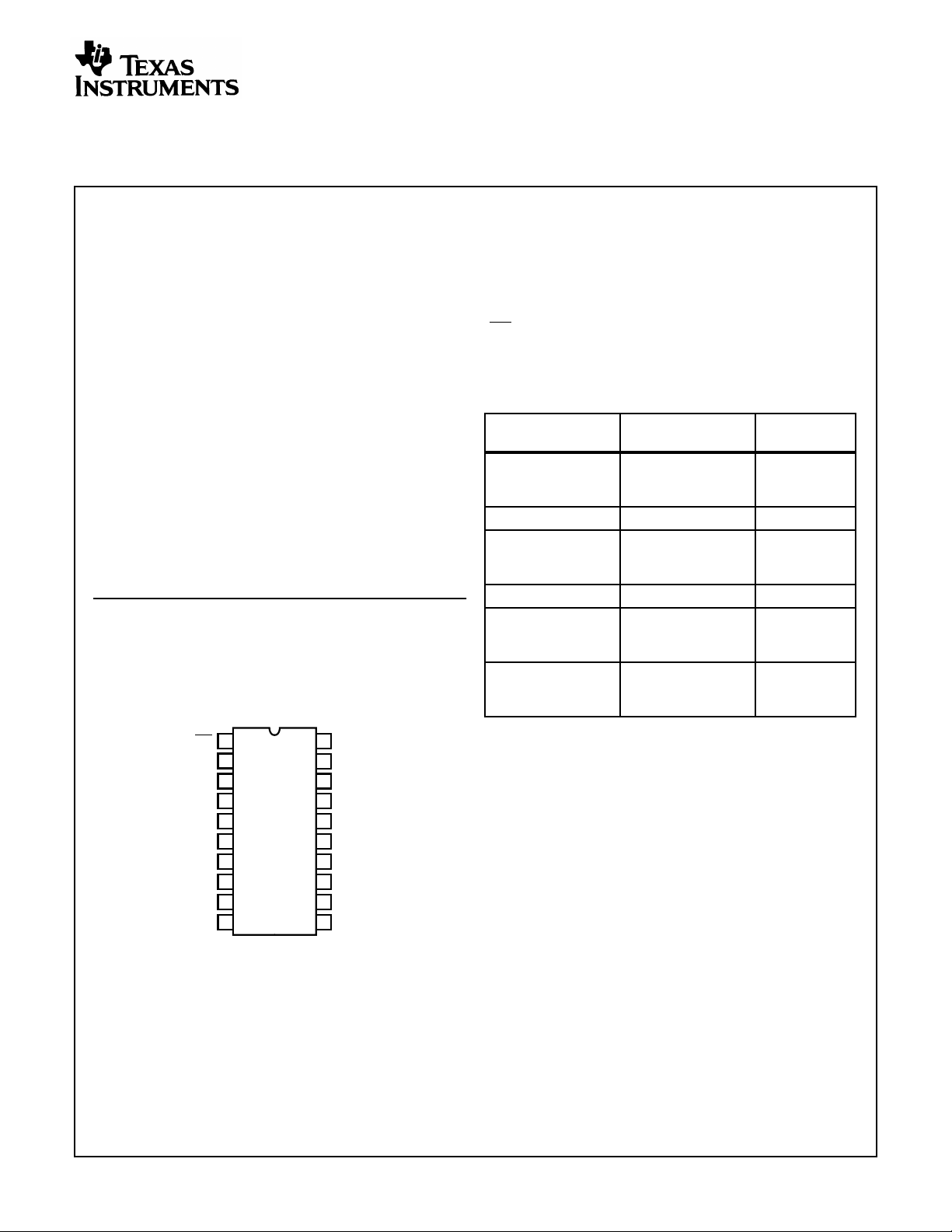
Pinout
CD54AC273, CD54ACT273
(CDIP)
CD74AC273, CD74ACT273
(PDIP, SOIC)
TOP VIEW
MR
Q0
D0
D1
Q1
Q2
D2
D3
Q3
GND
1
2
3
4
5
6
7
8
9
10
V
20
CC
Q7
19
D7
18
D6
17
Q6
16
Q5
15
D5
14
D4
13
12
Q4
11
CP
Octal D Flip-Flop with Reset
Description
The ’AC273 and ’ACT273 devices are octal D-type flip-flops
with reset that utilize advanced CMOS logic technology.
Information at the D input is transferred to the Q output on
the positive-going edge of the clock pulse. All eight flip-flops
are controlled by a common clock (CP) and a common reset
(
MR). Resetting is accomplished by a low voltage level
independent of the clock.
Ordering Information
PART
NUMBER
CD74AC273E 0oC to 70oC
CD54AC273F3A -55oC to 125oC 20 Ld CDIP
CD74ACT273E 0oC to 70oC
CD54ACT273F3A -55oC to 125oC 20 Ld CDIP
CD74AC273M 0oC to 70oC
CD74ACT273M 0oC to 70oC
NOTES:
1. When ordering, use the entirepartnumber. Add the suffix 96 to
obtain the variant in the tape and reel.
2. Waferand die for this part number is available which meets all
electrical specifications. Please contact your local sales office for
ordering information.
TEMPERATURE
RANGE PACKAGE
20 Ld PDIP
-40oC to 85oC
-55oC to 125oC
20 Ld PDIP
-40oC to 85oC
-55oC to 125oC
20 Ld SOIC
-40oC to 85oC
-55oC to 125oC
20 Ld SOIC
-40oC to 85oC
-55oC to 125oC
CAUTION: These devices are sensitive to electrostatic discharge. Users should follow proper IC Handling Procedures.
FAST™ is a Trademark of Fairchild Semiconductor.
Copyright
© 2002, Texas Instruments Incorporated
1
Page 2
CD54AC273, CD74AC273, CD54ACT273, CD74ACT273
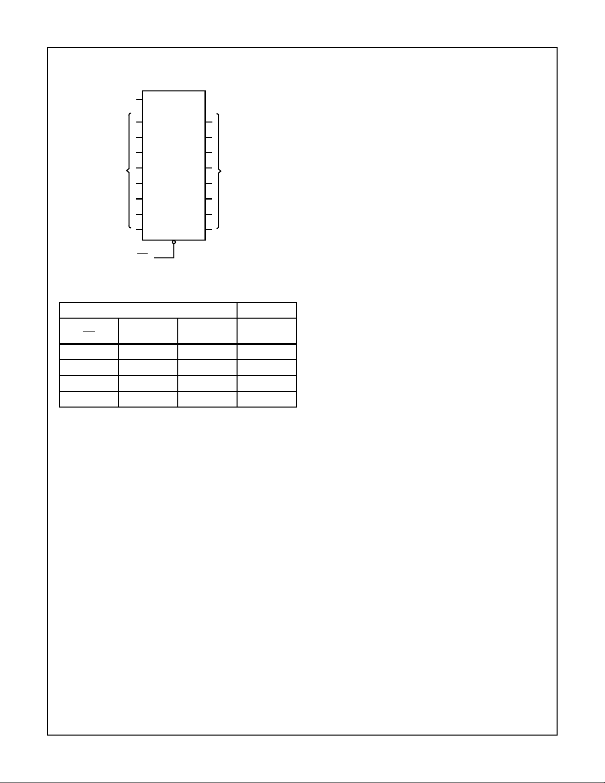
Functional Diagram
CLOCK
CP
DAT A
INPUTS
RESET MR
D0
D1
D2
D3
D4
D5
D6
D7
Q0
Q1
Q2
Q3
Q4
Q5
Q6
Q7
DAT A
OUTPUTS
TRUTH TABLE
INPUTS OUTPUTS
RESET
(MR)
CLOCK
CP
DATA
Dn Qn
LXXL
H ↑ HH
H ↑ LL
HLXQ0
H = High level (steady state), L = Low level (steady state), X = Irrelevant, ↑ = Transition from Low to High level, Q0 = The level of Q
before the indicated steady-state input conditions were established.
2
Page 3
CD54AC273, CD74AC273, CD54ACT273, CD74ACT273
Absolute Maximum Ratings Thermal Information
DC Supply Voltage, VCC. . . . . . . . . . . . . . . . . . . . . . . . -0.5V to 6V
DC Input Diode Current, I
IK
For VI < -0.5V or VI > VCC + 0.5V. . . . . . . . . . . . . . . . . . . . . .±20mA
DC Output Diode Current, I
OK
For VO < -0.5V or VO > VCC + 0.5V . . . . . . . . . . . . . . . . . . . .±50mA
DC Output Source or Sink Current per Output Pin, I
O
For VO > -0.5V or VO < VCC + 0.5V . . . . . . . . . . . . . . . . . . . .±50mA
DC VCC or Ground Current, I
CC orIGND
(Note 3) . . . . . . . . .±100mA
Operating Conditions
Temperature Range, TA . . . . . . . . . . . . . . . . . . . . . . -55oC to 125oC
Supply Voltage Range, VCC (Note 4)
AC Types. . . . . . . . . . . . . . . . . . . . . . . . . . . . . . . . . . .1.5V to 5.5V
ACT Types . . . . . . . . . . . . . . . . . . . . . . . . . . . . . . . . .4.5V to 5.5V
DC Input or Output Voltage, VI, VO . . . . . . . . . . . . . . . . . 0V to V
Input Rise and Fall Slew Rate, dt/dv
AC Types, 1.5V to 3V . . . . . . . . . . . . . . . . . . . . . . . . . 50ns (Max)
AC Types, 3.6V to 5.5V. . . . . . . . . . . . . . . . . . . . . . . . 20ns (Max)
ACT Types, 4.5V to 5.5V. . . . . . . . . . . . . . . . . . . . . . . 10ns (Max)
CAUTION: Stresses above those listed in “Absolute Maximum Ratings” may cause permanent damage to the device. This is a stress only rating and operation
of the device at these or any other conditions above those indicated in the operational sections of this specification is not implied.
NOTES:
3. For up to 4 outputs per device, add ±25mA for each additional output.
4. Unless otherwise specified, all voltages are referenced to ground.
5. The package thermal impedance is calculated in accordance with JESD 51.
Thermal Resistance, θJA(Typical, Note 5)
E Package. . . . . . . . . . . . . . . . . . . . . . . . . . . . . . . . . . . . .69oC/W
M Package. . . . . . . . . . . . . . . . . . . . . . . . . . . . . . . . . . . . .58oC/W
Maximum Junction Temperature (Plastic Package) . . . . . . . . . . 150oC
Maximum Storage Temperature Range . . . . . . . . . .-65oC to 150oC
Maximum Lead Temperature (Soldering 10s) . . . . . . . . . . . . . 300oC
CC
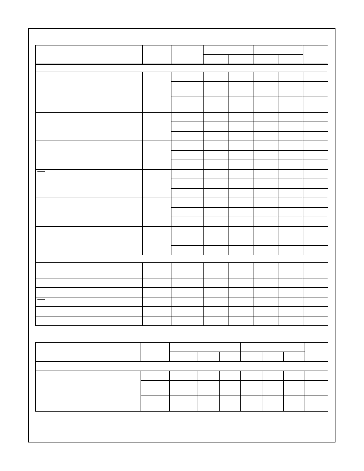
DC Electrical Specifications
PARAMETER SYMBOL
AC TYPES
High Level Input Voltage V
Low Level Input Voltage V
High Level Output Voltage V
IH
IL
OH
TEST
CONDITIONS
(V) IO(mA) MIN MAX MIN MAX MIN MAX
I
V
CC
(V)
25
o
C
-40oC TO
85oC
-55oC TO
125oC
- - 1.5 1.2 - 1.2 - 1.2 - V
3 2.1 - 2.1 - 2.1 - V
5.5 3.85 - 3.85 - 3.85 - V
- - 1.5 - 0.3 - 0.3 - 0.3 V
3 - 0.9 - 0.9 - 0.9 V
5.5 - 1.65 - 1.65 - 1.65 V
VIH or V
-0.05 1.5 1.4 - 1.4 - 1.4 - V
IL
-0.05 3 2.9 - 2.9 - 2.9 - V
-0.05 4.5 4.4 - 4.4 - 4.4 - V
-4 3 2.58 - 2.48 - 2.4 - V
-24 4.5 3.94 - 3.8 - 3.7 - V
-75
5.5 - - 3.85 - - - V
(Note 6, 7)
-50
5.5----3.85 - V
(Note 6, 7)
UNITSV
3
Page 4
CD54AC273, CD74AC273, CD54ACT273, CD74ACT273
DC Electrical Specifications (Continued)
PARAMETER SYMBOL
Low Level Output Voltage V
OL
TEST
CONDITIONS
(V) IO(mA) MIN MAX MIN MAX MIN MAX
I
VIH or V
0.05 1.5 - 0.1 - 0.1 - 0.1 V
IL
V
CC
(V)
25
o
C
0.05 3 - 0.1 - 0.1 - 0.1 V
0.05 4.5 - 0.1 - 0.1 - 0.1 V
12 3 - 0.36 - 0.44 - 0.5 V
24 4.5 - 0.36 - 0.44 - 0.5 V
75
5.5 - - - 1.65 - - V
(Note 6, 7)
50
5.5-----1.65 V
(Note 6, 7)
Input Leakage Current I
I
VCC or
- 5.5 - ±0.1 - ±1-±1 µA
GND
Quiescent Supply Current
MSI
I
CC
VCC or
GND
0 5.5 - 8 - 80 - 160 µA
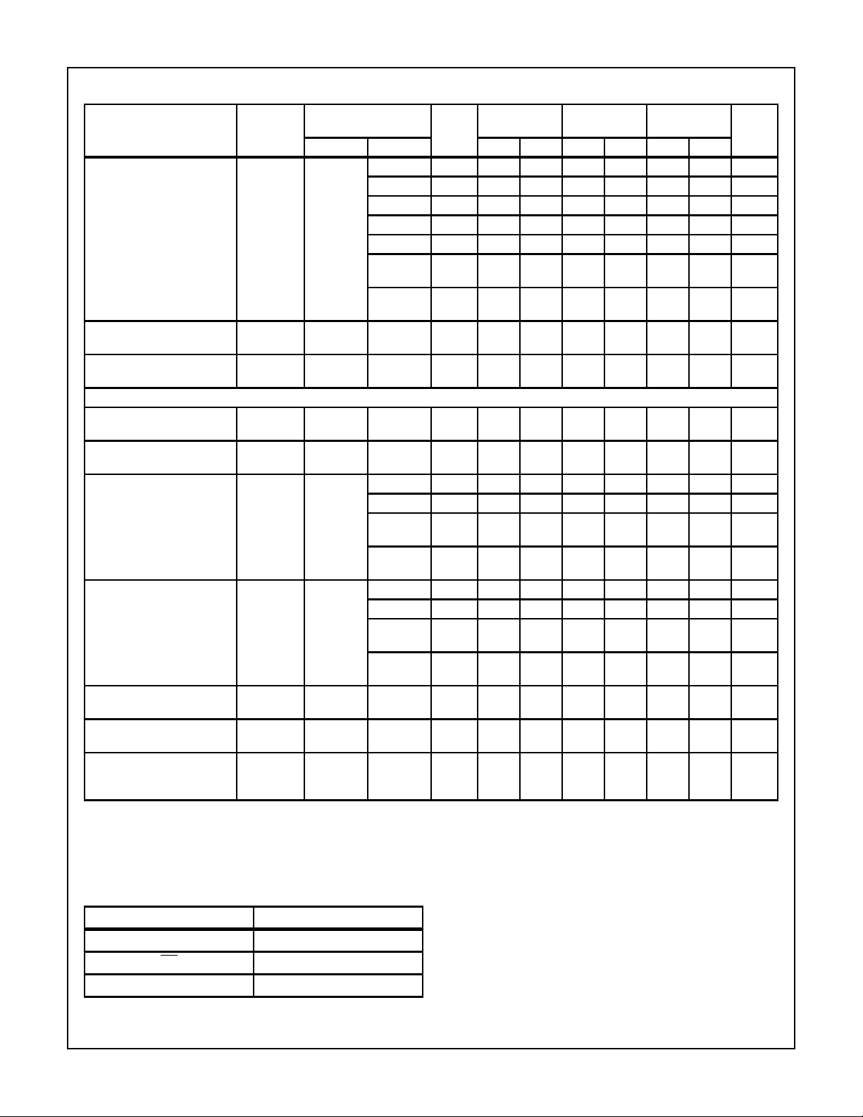
ACT TYPES
High Level Input Voltage V
IH
- - 4.5 to
2-2-2-V
5.5
Low Level Input Voltage V
IL
- - 4.5 to
- 0.8 - 0.8 - 0.8 V
5.5
High Level Output Voltage V
OH
VIH or V
-0.05 4.5 4.4 - 4.4 - 4.4 - V
IL
-24 4.5 3.94 - 3.8 - 3.7 - V
-75
5.5 - - 3.85 - - - V
(Note 6, 7)
-50
5.5----3.85 - V
(Note 6, 7)
Low Level Output Voltage V
OL
VIH or V
0.05 4.5 - 0.1 - 0.1 - 0.1 V
IL
24 4.5 - 0.36 - 0.44 - 0.5 V
75
5.5 - - - 1.65 - - V
(Note 6, 7)
50
5.5-----1.65 V
(Note 6, 7)
Input Leakage Current I
I
VCC or
- 5.5 - ±0.1 - ±1-±1 µA
GND
Quiescent Supply Current
MSI
AdditionalSupply Current per
Input Pin TTL Inputs High
I
CC
VCC or
GND
∆I
CC
V
CC
-2.1
0 5.5 - 8 - 80 - 160 µA
- 4.5 to
- 2.4 - 2.8 - 3 mA
5.5
1 Unit Load
NOTES:
6. Test one output at a time for a 1-second maximum duration. Measurement is made by forcing current and measuring voltage to minimize
power dissipation.
7. Test verifies a minimum 50Ω transmission-line-drive capability at 85
o
C, 75Ω at 125oC.
-40oC TO
85oC
-55oC TO
125oC
UNITSV
ACT Input Load Table
INPUT UNIT LOAD
Dn 0.5
MR 0.57
CP 1
NOTE: Unit load is ∆ICClimit specified in DC Electrical Specifications
Table, e.g., 2.4mA max at 25oC.
4
Page 5
CD54AC273, CD74AC273, CD54ACT273, CD74ACT273
Prerequisite For Switching Function
PARAMETER SYMBOL VCC (V)
AC TYPES
Data to CP Set-Up Time t
Hold Time t
Removal Time, MR to CP t
MR Pulse Width t
CP Pulse Width t
CP Frequency f
ACT TYPES
Data to CP Set-Up Time t
Hold Time t
Removal Time MR to CP t
MR Pulse Width t
CP Pulse Width t
CP Frequency f
SU
H
REM
W
W
MAX
SU
H
REM
W
W
MAX
-40oC TO 85oC -55oC TO 125oC
UNITSMIN MAX MIN MAX
1.5 2 - 2 - ns
3.3
2-2-ns
(Note 9)
5
2-2-ns
(Note 10)
1.5 2 - 2 - ns
3.3 2 - 2 - ns
52-2-ns
1.5 2 - 2 - ns
3.3 2 - 2 - ns
52-2-ns
1.5 55 - 63 - ns
3.3 6.1 - 7 - ns
5 4.4 - 5 - ns
1.5 55 - 63 - ns
3.3 6.1 - 7 - ns
5 4.4 - 5 - ns
1.5 9 - 8 - MHz
3.3 81 - 71 - MHz
5 114 - 100 - MHz
5
2-2-ns
(Note 10)
52-2-ns
52-2-ns
5 4.4 - 5 - ns
5 5.3 - 6 - ns
5 97 - 85 - MHz
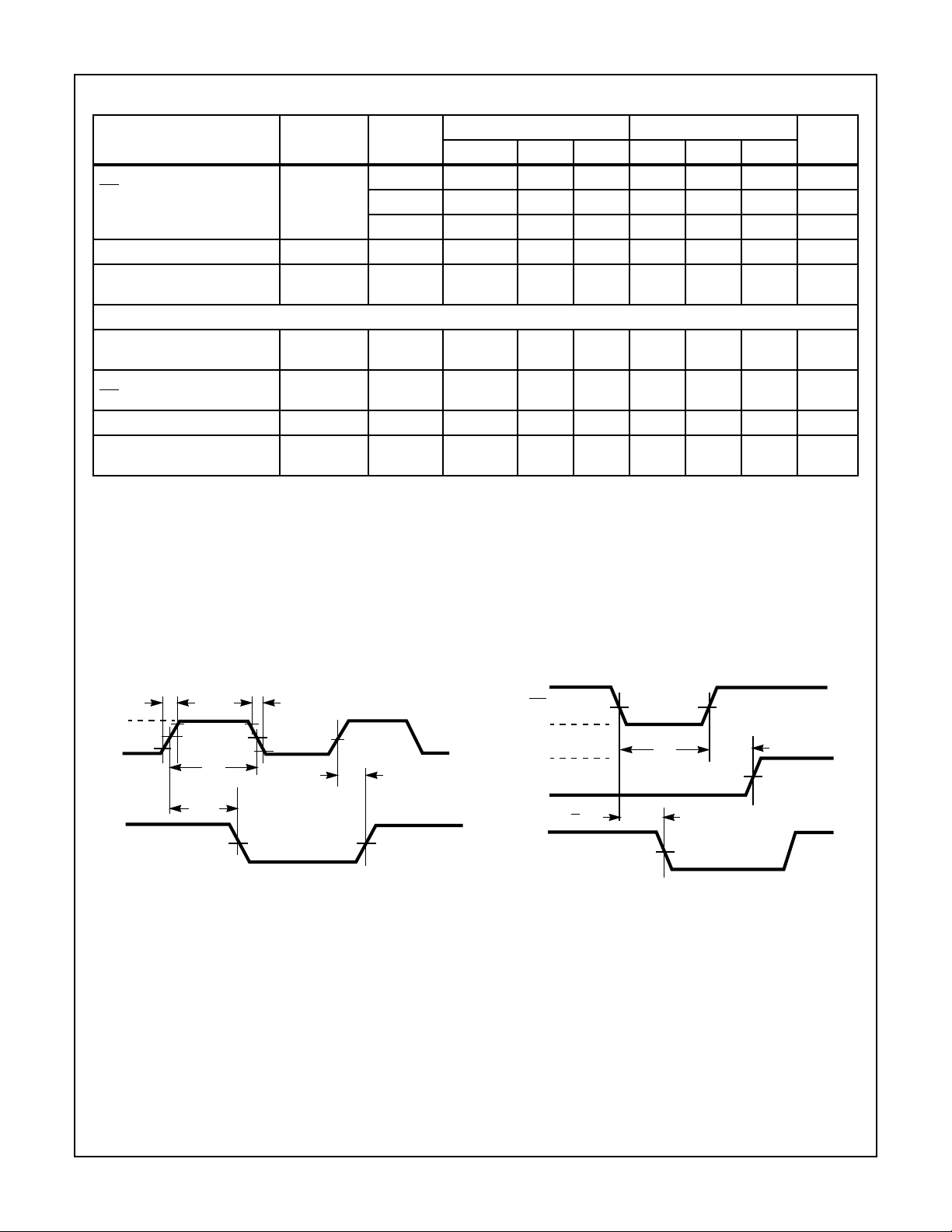
Switching Specifications Input t
PARAMETER SYMBOL VCC (V)
AC TYPES
Propagation Delay,
CP to Qn
t
PLH
, tf = 3ns, CL= 50pF (Worst Case)
r
, t
PHL
1.5 - - 154 - - 169 ns
3.3
4.9 - 17.2 4.7 - 18.9 ns
(Note 9)
5
3.5 - 12.3 3.4 - 13.5 ns
(Note 10)
5
-40oC TO 85oC -55oC TO 125oC
UNITSMIN TYP MAX MIN TYP MAX
Page 6
CD54AC273, CD74AC273, CD54ACT273, CD74ACT273
Switching Specifications Input t
, tf = 3ns, CL= 50pF (Worst Case) (Continued)
r
-40oC TO 85oC -55oC TO 125oC
PARAMETER SYMBOL VCC (V)
Propagation Delay,
MR to Qn
t
PLH
, t
PHL
1.5 - - 154 - - 169 ns
3.3 4.9 - 17.2 4.7 - 18.9 ns
5 3.5 - 12.3 3.4 - 13.5 ns
Input Capacitance C
Power Dissipation Capacitance C
I
PD
- - -10- -10pF
- - 45 - - 45 - pF
(Note 11)
ACT TYPES
Propagation Delay,
CP to Qn
Propagation Delay,
t
PLH
t
PLH
, t
PHL
5
3.5 - 12.3 3.4 - 13.5 ns
(Note 10)
, t
PHL
5 3.5 - 12.3 3.4 - 13.5 ns
MR to Qn
Input Capacitance C
Power Dissipation Capacitance C
I
PD
- - -10- -10pF
- - 45 - - 45 - pF
(Note 11)
NOTES:
8. Limits tested 100%.
9. 3.3V Min is at 3.6V, Max is at 3V.
10. 5V Min is at 5.5V, Max is at 4.5V.
11. CPD is used to determine the dynamic power consumption per flip-flop.
AC: PD = CPD V
ACT: PD=CPDV
2
fi= ∑ (CL V
CC
2
CC
fi+ ∑ (CLV
2
fo)
CC
2
fo)+VCC∆ICCwhere fi= input frequency, fo= output frequency, CL= output load capacitance,
CC
VCC = supply voltage.
UNITSMIN TYP MAX MIN TYP MAX
INPUT
LEVEL
CP
Q
10%
90%
V
S
t
t
r
PHL
t
f
V
S
10%
t
W
V
S
V
S
t
PLH
V
S
FIGURE 1. PROPAGATION DELAY TIMES AND CLOCK
PULSE WIDTH
INPUT
LEVEL
MR
GND
INPUT
CP
(
Q)
Q
V
t
S
PLH
V
S
t
t
W
V
S
REM
V
S
FIGURE 2. PREREQUISITE AND PROPAGATION DELAY
TIMES FOR MASTER RESET
6
Page 7

CD54AC273, CD74AC273, CD54ACT273, CD74ACT273
OUTPUT
LEVEL
D
V
S
tSU(L)
CP
FIGURE 3. PREREQUISITE FOR CLOCK
DUT
V
S
V
S
OUTPUT
V
S
(L)
t
H
R
L
tSU(H)
(NOTE)
500Ω
V
S
tH(H)
V
S
OUTPUT
LOAD
C
L
50pF
NOTE: For AC Series Only: When VCC = 1.5V, RL = 1kΩ.
AC ACT
Input Level V
Input Switching Voltage, V
Output Switching Voltage, V
S
S
0.5 V
0.5 V
CC
CC
CC
FIGURE 4. PROPAGATION DELAY TIMES
3V
1.5V
0.5 V
CC
7
Page 8

PACKAGE OPTION ADDENDUM
www.ti.com
PACKAGING INFORMATION
Orderable Device Status
CD54AC273F3A ACTIVE CDIP J 20 1 TBD A42 SNPB N / A for Pkg Type
CD54ACT273F3A ACTIVE CDIP J 20 1 TBD A42 SNPB N / A for Pkg Type
CD74AC273E ACTIVE PDIP N 20 20 Pb-Free
CD74AC273EE4 ACTIVE PDIP N 20 20 Pb-Free
CD74AC273M ACTIVE SOIC DW 20 25 Green (RoHS &
CD74AC273M96 ACTIVE SOIC DW 20 2000 Green (RoHS &
CD74AC273M96E4 ACTIVE SOIC DW 20 2000 Green (RoHS &
CD74AC273M96G4 ACTIVE SOIC DW 20 2000 Green (RoHS &
CD74AC273ME4 ACTIVE SOIC DW 20 25 Green (RoHS &
CD74AC273MG4 ACTIVE SOIC DW 20 25 Green (RoHS &
CD74AC273SM OBSOLETE SSOP DB 20 Green (RoHS &
CD74ACT273E ACTIVE PDIP N 20 20 Pb-Free
CD74ACT273EE4 ACTIVE PDIP N 20 20 Pb-Free
CD74ACT273M ACTIVE SOIC DW 20 25 Green (RoHS &
CD74ACT273M96 ACTIVE SOIC DW 20 2000 Green (RoHS &
CD74ACT273M96E4 ACTIVE SOIC DW 20 2000 Green (RoHS &
CD74ACT273M96G4 ACTIVE SOIC DW 20 2000 Green (RoHS &
CD74ACT273ME4 ACTIVE SOIC DW 20 25 Green (RoHS &
CD74ACT273MG4 ACTIVE SOIC DW 20 25 Green (RoHS &
CD74ACT273PW ACTIVE TSSOP PW 20 70 Green (RoHS &
CD74ACT273PWE4 ACTIVE TSSOP PW 20 70 Green (RoHS &
CD74ACT273PWG4 ACTIVE TSSOP PW 20 70 Green (RoHS &
CD74ACT273PWR ACTIVE TSSOP PW 20 2000 Green (RoHS &
CD74ACT273PWRE4 ACTIVE TSSOP PW 20 2000 Green (RoHS &
CD74ACT273PWRG4 ACTIVE TSSOP PW 20 2000 Green (RoHS &
CD74ACT273SM OBSOLETE SSOP DB 20 Green (RoHS & CU NIPDAU Level-1-260C-UNLIM
(1)
Package
Type
Package
Drawing
Pins Package
Qty
Eco Plan
no Sb/Br)
no Sb/Br)
no Sb/Br)
no Sb/Br)
no Sb/Br)
no Sb/Br)
no Sb/Br)
no Sb/Br)
no Sb/Br)
no Sb/Br)
no Sb/Br)
no Sb/Br)
no Sb/Br)
no Sb/Br)
no Sb/Br)
no Sb/Br)
no Sb/Br)
no Sb/Br)
no Sb/Br)
(RoHS)
(RoHS)
(RoHS)
(RoHS)
(2)
Lead/Ball Finish MSL Peak Temp
CU NIPDAU N / A for Pkg Type
CU NIPDAU N / A for Pkg Type
CU NIPDAU Level-1-260C-UNLIM
CU NIPDAU Level-1-260C-UNLIM
CU NIPDAU Level-1-260C-UNLIM
CU NIPDAU Level-1-260C-UNLIM
CU NIPDAU Level-1-260C-UNLIM
CU NIPDAU Level-1-260C-UNLIM
CU NIPDAU Level-1-260C-UNLIM
CU NIPDAU N / A for Pkg Type
CU NIPDAU N / A for Pkg Type
CU NIPDAU Level-1-260C-UNLIM
CU NIPDAU Level-1-260C-UNLIM
CU NIPDAU Level-1-260C-UNLIM
CU NIPDAU Level-1-260C-UNLIM
CU NIPDAU Level-1-260C-UNLIM
CU NIPDAU Level-1-260C-UNLIM
CU NIPDAU Level-1-260C-UNLIM
CU NIPDAU Level-1-260C-UNLIM
CU NIPDAU Level-1-260C-UNLIM
CU NIPDAU Level-1-260C-UNLIM
CU NIPDAU Level-1-260C-UNLIM
CU NIPDAU Level-1-260C-UNLIM
9-Oct-2007
(3)
Addendum-Page 1
Page 9

PACKAGE OPTION ADDENDUM
www.ti.com
Orderable Device Status
(1)
Package
Type
Package
Drawing
Pins Package
Qty
Eco Plan
(2)
Lead/Ball Finish MSL Peak Temp
9-Oct-2007
(3)
no Sb/Br)
CD74ACT273SM96 ACTIVE SSOP DB 20 2000 Green (RoHS &
CU NIPDAU Level-1-260C-UNLIM
no Sb/Br)
CD74ACT273SM96E4 ACTIVE SSOP DB 20 2000 Green (RoHS &
CU NIPDAU Level-1-260C-UNLIM
no Sb/Br)
CD74ACT273SM96G4 ACTIVE SSOP DB 20 2000 Green (RoHS &
CU NIPDAU Level-1-260C-UNLIM
no Sb/Br)
(1)
The marketing status values are defined as follows:
ACTIVE: Product device recommended for new designs.
LIFEBUY: TI has announced that the device will be discontinued, and a lifetime-buy period is in effect.
NRND: Not recommended for new designs. Device is in production to support existing customers, but TI does not recommend using this part in
a new design.
PREVIEW: Device has been announced but is not in production. Samples may or may not be available.
OBSOLETE: TI has discontinued the production of the device.
(2)
Eco Plan - The planned eco-friendly classification: Pb-Free (RoHS), Pb-Free (RoHS Exempt), or Green (RoHS & no Sb/Br) - please check
http://www.ti.com/productcontent for the latest availability information and additional product content details.
TBD: The Pb-Free/Green conversion plan has not been defined.
Pb-Free (RoHS): TI's terms "Lead-Free" or "Pb-Free" mean semiconductor products that are compatible with the current RoHS requirements
for all 6 substances, including the requirement that lead not exceed 0.1% by weight in homogeneous materials. Where designed to be soldered
at high temperatures, TI Pb-Free products are suitable for use in specified lead-free processes.
Pb-Free (RoHS Exempt): This component has a RoHS exemption for either 1) lead-based flip-chip solder bumps used between the die and
package, or 2) lead-based die adhesive used between the die and leadframe. The component is otherwise considered Pb-Free (RoHS
compatible) as defined above.
Green (RoHS & no Sb/Br): TI defines "Green" to mean Pb-Free (RoHS compatible), and free of Bromine (Br) and Antimony (Sb) based flame
retardants (Br or Sb do not exceed 0.1% by weight in homogeneous material)
(3)
MSL, Peak Temp. -- The Moisture Sensitivity Level rating according to the JEDEC industry standard classifications, and peak solder
temperature.
Important Information and Disclaimer:The information provided on this page represents TI's knowledge and belief as of the date that it is
provided. TI bases its knowledge and belief on information provided by third parties, and makes no representation or warranty as to the
accuracy of such information. Efforts are underway to better integrate information from third parties. TI has taken and continues to take
reasonable steps to provide representative and accurate information but may not have conducted destructive testing or chemical analysis on
incoming materials and chemicals. TI and TI suppliers consider certain information to be proprietary, and thus CAS numbers and other limited
information may not be available for release.
In no event shall TI's liability arising out of such information exceed the total purchase price of the TI part(s) at issue in this document sold by TI
to Customer on an annual basis.
Addendum-Page 2
Page 10

PACKAGE MATERIALS INFORMATION
www.ti.com
TAPE AND REEL INFORMATION
11-Mar-2008
*All dimensions are nominal
Device Package
Type
CD74AC273M96 SOIC DW 20 2000 330.0 24.4 10.8 13.0 2.7 12.0 24.0 Q1
CD74ACT273M96 SOIC DW 20 2000 330.0 24.4 10.8 13.0 2.7 12.0 24.0 Q1
CD74ACT273PWR TSSOP PW 20 2000 330.0 16.4 6.95 7.1 1.6 8.0 16.0 Q1
CD74ACT273SM96 SSOP DB 20 2000 330.0 16.4 8.2 7.5 2.5 12.0 16.0 Q1
Package
Drawing
Pins SPQ Reel
Diameter
(mm)
Reel
Width
W1 (mm)
A0 (mm) B0 (mm) K0 (mm) P1
(mm)W(mm)
Pin1
Quadrant
Pack Materials-Page 1
Page 11

PACKAGE MATERIALS INFORMATION
www.ti.com
11-Mar-2008
*All dimensions are nominal
Device Package Type Package Drawing Pins SPQ Length (mm) Width (mm) Height (mm)
CD74AC273M96 SOIC DW 20 2000 346.0 346.0 41.0
CD74ACT273M96 SOIC DW 20 2000 346.0 346.0 41.0
CD74ACT273PWR TSSOP PW 20 2000 346.0 346.0 33.0
CD74ACT273SM96 SSOP DB 20 2000 346.0 346.0 33.0
Pack Materials-Page 2
Page 12

MECHANICAL DATA
MSSO002E – JANUARY 1995 – REVISED DECEMBER 2001
DB (R-PDSO-G**) PLASTIC SMALL-OUTLINE
28 PINS SHOWN
0,65
28
1
2,00 MAX
0,38
0,22
15
14
A
0,05 MIN
0,15
M
5,60
5,00
Seating Plane
8,20
7,40
0,10
0,25
0,09
0°–ā8°
Gage Plane
0,25
0,95
0,55
PINS **
DIM
A MAX
A MIN
NOTES: A. All linear dimensions are in millimeters.
B. This drawing is subject to change without notice.
C. Body dimensions do not include mold flash or protrusion not to exceed 0,15.
D. Falls within JEDEC MO-150
14
6,50
6,50
5,905,90
2016
7,50
6,90
24
8,50
28
10,50
9,907,90
30
10,50
9,90
38
12,90
12,30
4040065 /E 12/01
POST OFFICE BOX 655303 • DALLAS, TEXAS 75265
Page 13

Page 14

MECHANICAL DATA
MTSS001C – JANUARY 1995 – REVISED FEBRUARY 1999
PW (R-PDSO-G**) PLASTIC SMALL-OUTLINE PACKAGE
14 PINS SHOWN
0,65
1,20 MAX
14
0,30
0,19
8
4,50
4,30
PINS **
7
Seating Plane
0,15
0,05
8
1
A
DIM
14
0,10
6,60
6,20
M
0,10
0,15 NOM
0°–8°
2016
Gage Plane
24
0,25
0,75
0,50
28
A MAX
A MIN
NOTES: A. All linear dimensions are in millimeters.
B. This drawing is subject to change without notice.
C. Body dimensions do not include mold flash or protrusion not to exceed 0,15.
D. Falls within JEDEC MO-153
3,10
2,90
5,10
4,90
5,10
4,90
6,60
6,40
7,90
7,70
9,80
9,60
4040064/F 01/97
POST OFFICE BOX 655303 • DALLAS, TEXAS 75265
Page 15

Page 16

Page 17

IMPORTANT NOTICE
Texas Instruments Incorporated and its subsidiaries (TI) reserve the right to make corrections, modifications, enhancements, improvements,
and other changes to its products and services at any time and to discontinue any product or service without notice. Customers should
obtain the latest relevant information before placing orders and should verify that such information is current and complete. All products are
sold subject to TI’s terms and conditions of sale supplied at the time of order acknowledgment.
TI warrants performance of its hardware products to the specifications applicable at the time of sale in accordance with TI’s standard
warranty. Testing and other quality control techniques are used to the extent TI deems necessary to support this warranty. Except where
mandated by government requirements, testing of all parameters of each product is not necessarily performed.
TI assumes no liability for applications assistance or customer product design. Customers are responsible for their products and
applications using TI components. To minimize the risks associated with customer products and applications, customers should provide
adequate design and operating safeguards.
TI does not warrant or represent that any license, either express or implied, is granted under any TI patent right, copyright, mask work right,
or other TI intellectual property right relating to any combination, machine, or process in which TI products or services are used. Information
published by TI regarding third-party products or services does not constitute a license from TI to use such products or services or a
warranty or endorsement thereof. Use of such information may require a license from a third party under the patents or other intellectual
property of the third party, or a license from TI under the patents or other intellectual property of TI.
Reproduction of TI information in TI data books or data sheets is permissible only if reproduction is without alteration and is accompanied
by all associated warranties, conditions, limitations, and notices. Reproduction of this information with alteration is an unfair and deceptive
business practice. TI is not responsible or liable for such altered documentation. Information of third parties may be subject to additional
restrictions.
Resale of TI products or services with statements different from or beyond the parameters stated by TI for that product or service voids all
express and any implied warranties for the associated TI product or service and is an unfair and deceptive business practice. TI is not
responsible or liable for any such statements.
TI products are not authorized for use in safety-critical applications (such as life support) where a failure of the TI product would reasonably
be expected to cause severe personal injury or death, unless officers of the parties have executed an agreement specifically governing
such use. Buyers represent that they have all necessary expertise in the safety and regulatory ramifications of their applications, and
acknowledge and agree that they are solely responsible for all legal, regulatory and safety-related requirements concerning their products
and any use of TI products in such safety-critical applications, notwithstanding any applications-related information or support that may be
provided by TI. Further, Buyers must fully indemnify TI and its representatives against any damages arising out of the use of TI products in
such safety-critical applications.
TI products are neither designed nor intended for use in military/aerospace applications or environments unless the TI products are
specifically designated by TI as military-grade or "enhanced plastic." Only products designated by TI as military-grade meet military
specifications. Buyers acknowledge and agree that any such use of TI products which TI has not designated as military-grade is solely at
the Buyer's risk, and that they are solely responsible for compliance with all legal and regulatory requirements in connection with such use.
TI products are neither designed nor intended for use in automotive applications or environments unless the specific TI products are
designated by TI as compliant with ISO/TS 16949 requirements. Buyers acknowledge and agree that, if they use any non-designated
products in automotive applications, TI will not be responsible for any failure to meet such requirements.
Following are URLs where you can obtain information on other Texas Instruments products and application solutions:
Products Applications
Amplifiers amplifier.ti.com Audio www.ti.com/audio
Data Converters dataconverter.ti.com Automotive www.ti.com/automotive
DSP dsp.ti.com Broadband www.ti.com/broadband
Clocks and Timers www.ti.com/clocks Digital Control www.ti.com/digitalcontrol
Interface interface.ti.com Medical www.ti.com/medical
Logic logic.ti.com Military www.ti.com/military
Power Mgmt power.ti.com Optical Networking www.ti.com/opticalnetwork
Microcontrollers microcontroller.ti.com Security www.ti.com/security
RFID www.ti-rfid.com Telephony www.ti.com/telephony
RF/IF and ZigBee® Solutions www.ti.com/lprf Video & Imaging www.ti.com/video
Mailing Address: Texas Instruments, Post Office Box 655303, Dallas, Texas 75265
Copyright © 2008, Texas Instruments Incorporated
Wireless www.ti.com/wireless
 Loading...