

Page 1
查询CD54AC163供应商
CD54AC163, CD74AC163
4-BIT SYNCHRONOUS BINARY COUNTERS
SCHS299 – APRIL 2000
D
Internal Look-Ahead for Fast Counting
D
Carry Output for n-Bit Cascading
D
Synchronous Counting
D
Synchronously Programmable
D
Package Options Include Plastic
Small-Outline (M), Standard Plastic (E) and
Ceramic (F) DIPs
description
The CD54AC163 and CD74AC163 devices are
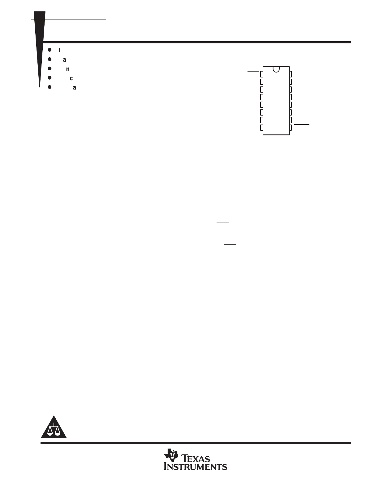
CD54AC163 ...F PACKAGE
CD74AC163 . . . E OR M PACKAGE
CLR
CLK
ENP
GND
(TOP VIEW)
1
2
A
3
B
4
C
5
D
6
7
8
16
15
14
13
12
11
10
9
V
CC
RCO
Q
A
Q
B
Q
C
Q
D
ENT
LOAD
4-bit binary counters. These synchronous,
presettable counters feature an internal carry
look-ahead for application in high-speed counting
designs. Synchronous operation is provided by having all flip-flops clocked simultaneously so that the outputs
change coincident with each other when instructed by the count-enable (ENP, ENT) inputs and internal gating.
This mode of operation eliminates the output counting spikes normally associated with synchronous
(ripple-clock) counters. A buffered clock (CLK) input triggers the four flip-flops on the rising (positive-going) edge
of the clock waveform.
The counters are fully programmable; that is, they can be preset to any number between 0 and 9 or 15.
Presetting is synchronous; therefore, setting up a low level at the load input disables the counter and causes
the outputs to agree with the setup data after the next clock pulse, regardless of the levels of the enable inputs.
The clear function is synchronous. A low level at the clear (CLR
) input sets all four of the flip-flop outputs low
after the next low-to-high transition of CLK, regardless of the levels of the enable inputs. This synchronous clear
allows the count length to be modified easily by decoding the Q outputs for the maximum count desired. The
active-low output of the gate used for decoding is connected to CLR to synchronously clear the counter to 0000
(LLLL).
The carry look-ahead circuitry provides for cascading counters for n-bit synchronous applications without
additional gating. ENP, ENT, and a ripple-carry output (RCO) are instrumental in accomplishing this function.
Both ENP and ENT must be high to count, and ENT is fed forward to enable RCO. Enabling RCO produces a
high-level pulse while the count is maximum (9 or 15 with Q
high). This high-level overflow ripple-carry pulse
A
can be used to enable successive cascaded stages. Transitions at ENP or ENT are allowed, regardless of the
level of CLK.
These devices feature a fully independent clock circuit. Changes at control inputs (ENP, ENT, or LOAD) that
modify the operating mode have no effect on the contents of the counter until clocking occurs. The function of
the counter (whether enabled, disabled, loading, or counting) is dictated solely by the conditions meeting the
stable setup and hold times.
The CD54AC163 is characterized for operation over the full military temperature range of –55°C to 125°C.
The CD74AC163 is characterized for operation from –40°C to 85°C.
Please be aware that an important notice concerning availability, standard warranty, and use in critical applications of
Texas Instruments semiconductor products and disclaimers thereto appears at the end of this data sheet.
PRODUCTION DATA information is current as of publication date.
Products conform to specifications per the terms of Texas Instruments
standard warranty. Production processing does not necessarily include
testing of all parameters.
POST OFFICE BOX 655303 • DALLAS, TEXAS 75265
Copyright 2000, Texas Instruments Incorporated
1
Page 2
CD54AC163, CD74AC163
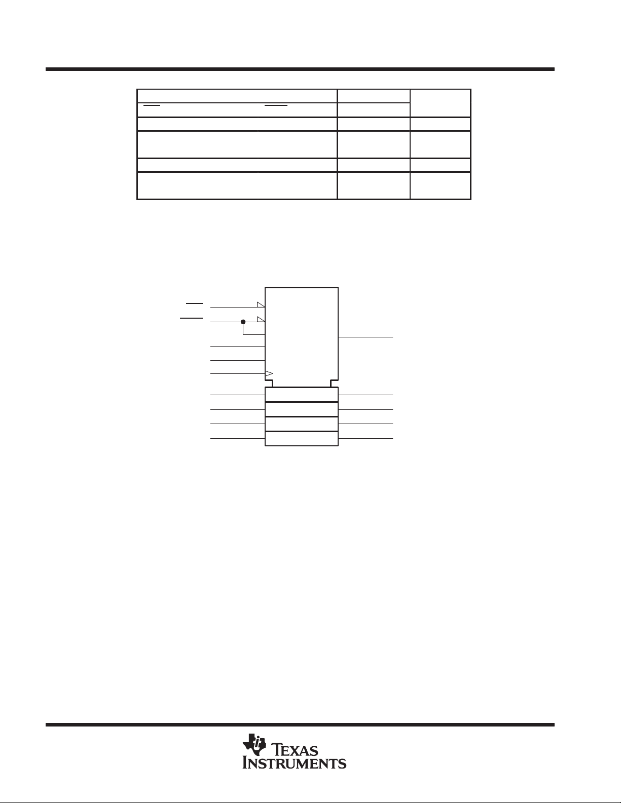
FUNCTION
Parallel load
Inhibit
4-BIT SYNCHRONOUS BINARY COUNTERS
SCHS299 – APRIL 2000
FUNCTION TABLE
INPUTS
CLR CLK ENP ENT LOAD A,B,C,D Q
L ↑ X X X X L L Reset (clear)
h ↑ X X l l L L
h ↑ XX l h HNote 1
h ↑ h h h X Count Note 1 Count
h X l X h X q
h X X l h X q
H = high level, L = low level, X = don’t care, h = high level one setup time prior to the CLK
low-to-high transition, l = low level one setup time prior to the CLK low-to-high transition, q = the
state of the referenced output prior to the CLK low-to-high transition, ↑ = CLK low-to-high
transition.
NOTE 1: The RCO output is high when ENT is high and the counter is at terminal count (HHHH).
OUTPUTS
RCO
n
Note 1
n
n
L
logic symbol
†
This symbol is in accordance with ANSI/IEEE Std 91-1984 and IEC Publication 617-12.
†
CTRDIV16
5CT=0
M1
M2
G3
G4
C5/2,3,4+
1,5D
3CT=15
[1]
[2]
[4]
[8]
CLR
LOAD
ENT
ENP
CLK
1
9
10
7
2
3
A
4
B
5
C
6
D
15
14
13
12
11
RCO
Q
A
Q
B
Q
C
Q
D
2
POST OFFICE BOX 655303 • DALLAS, TEXAS 75265
Page 3
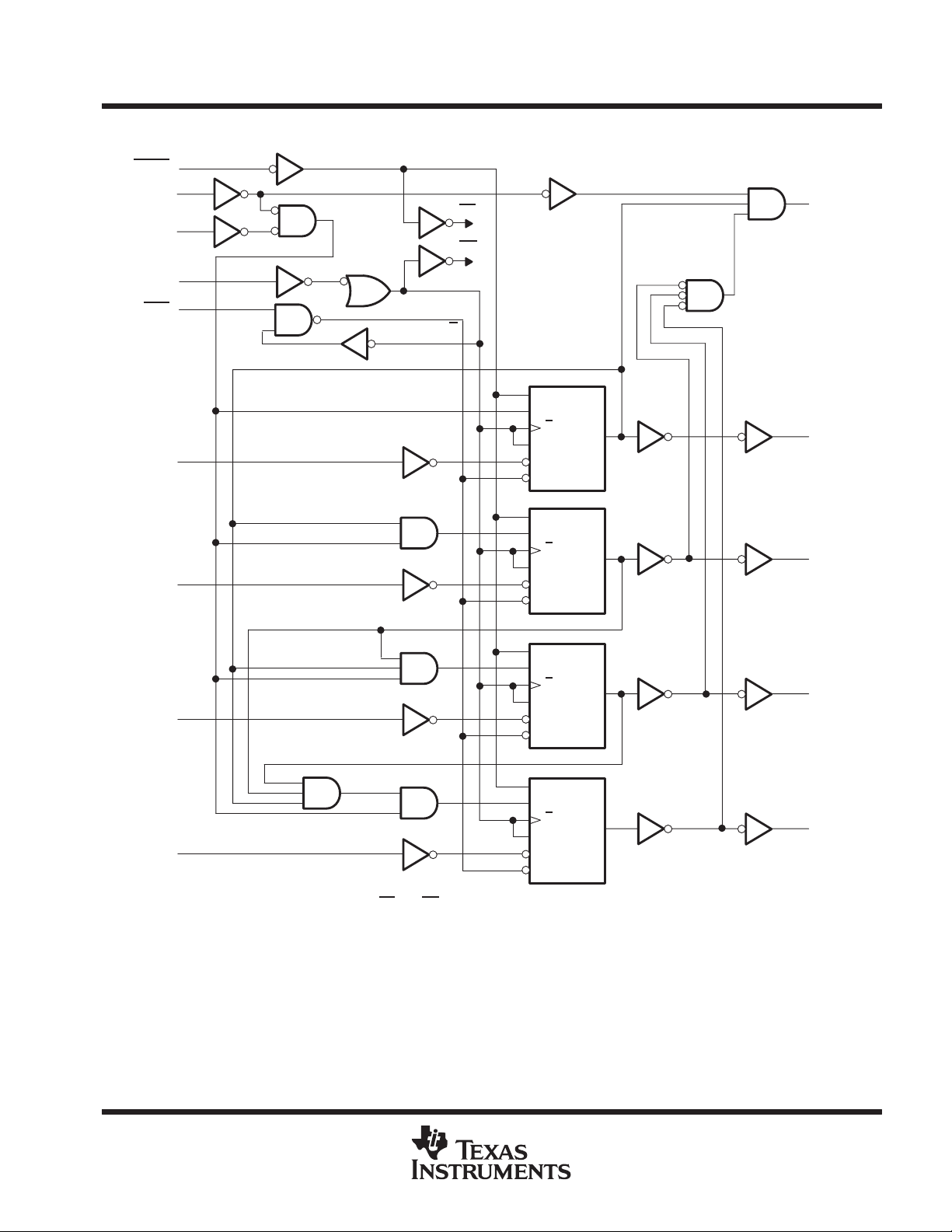
logic diagram (positive logic)
CD54AC163, CD74AC163
4-BIT SYNCHRONOUS BINARY COUNTERS
SCHS299 – APRIL 2000
LOAD
ENT
ENP
CLK
CLR
9
10
†
7
2
1
3
A
4
B
LD
†
CK
CK
R
LD
M1
G2
1
, 2T/1C3
G4
3D
4R
M1
G2
1
, 2T/1C3
G4
3D
4R
14
13
15
RCO
Q
A
Q
B
M1
G2
1, 2T/1C3
5
C
6
D
†
For simplicity, routing of complementary signals LD and CK is not shown on this overall logic diagram. The uses of these signals are shown
on the logic diagram of the D/T flip-flops.
G4
3D
4R
M1
G2
1
, 2T/1C3
G4
3D
4R
12
11
Q
C
Q
D
POST OFFICE BOX 655303 • DALLAS, TEXAS 75265
3
Page 4
CD54AC163, CD74AC163
4-BIT SYNCHRONOUS BINARY COUNTERS
SCHS299 – APRIL 2000
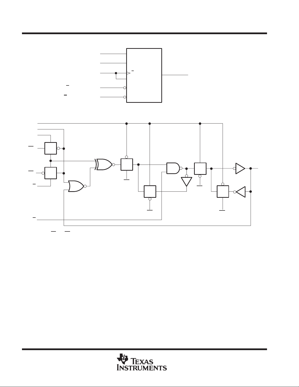
logic symbol, each D/T flip-flop
M1LD (Load)
G2TE (Toggle Enable)
CK (Clock)
(Inverted Data)
D
R
(Inverted Reset)
1, 2T/1C3
G4
3D
4R
logic diagram, each D/T flip-flop (positive logic)
CK
LD
TE
†
LD
LD
D
R
TG
TG
†
TG
†
CK
TG
CK
Q (Output)
TG
†
CK
†
TG
CK
†
Q
†
The origins of LD
4
and CK are shown in the logic diagram of the overall device.
POST OFFICE BOX 655303 • DALLAS, TEXAS 75265
Page 5

typical clear, preset, count, and inhibit sequence
The following sequence is illustrated below:
1. Clear outputs to zero (synchronous)
2. Preset to binary 12
3. Count to 13, 14, 15, 0, 1, and 2
4. Inhibit
CLR
LOAD
A
CD54AC163, CD74AC163
4-BIT SYNCHRONOUS BINARY COUNTERS
SCHS299 – APRIL 2000
Data
Inputs
Data
Outputs
CLK
ENP
ENT
Q
Q
Q
Q
RCO
B
C
D
A
B
C
D
Sync
Clear
12 13
Preset
14 15 0 1 2
Count Inhibit
POST OFFICE BOX 655303 • DALLAS, TEXAS 75265
5
Page 6
CD54AC163, CD74AC163
UNIT
∆t/∆vInput transition rise or fall rate
ns
4-BIT SYNCHRONOUS BINARY COUNTERS
SCHS299 – APRIL 2000
absolute maximum ratings over operating free-air temperature range
†
Supply voltage range, VCC –0.5 V to 6 V. . . . . . . . . . . . . . . . . . . . . . . . . . . . . . . . . . . . . . . . . . . . . . . . . . . . . . . . . .
Input clamp current, IIK (VI < 0 or VI > VCC) (see Note 2) ±20 mA. . . . . . . . . . . . . . . . . . . . . . . . . . . . . . . . . . . .
Output clamp current, I
(VO < 0 or VO > VCC) (see Note 2) ±50 mA. . . . . . . . . . . . . . . . . . . . . . . . . . . . . . . .
OK
Continuous output current, IO (VO = 0 to VCC) ±50 mA. . . . . . . . . . . . . . . . . . . . . . . . . . . . . . . . . . . . . . . . . . . . . .
Continuous current through VCC or GND ±100 mA. . . . . . . . . . . . . . . . . . . . . . . . . . . . . . . . . . . . . . . . . . . . . . . . . .
Package thermal impedance, θ
(see Note 3): E package 67°C/W. . . . . . . . . . . . . . . . . . . . . . . . . . . . . . . . . . .
JA
M package 73°C/W. . . . . . . . . . . . . . . . . . . . . . . . . . . . . . . . . .
Storage temperature range, T
†
Stresses beyond those listed under “absolute maximum ratings” may cause permanent damage to the device. These are stress ratings only, and
functional operation of the device at these or any other conditions beyond those indicated under “recommended operating conditions” is not
implied. Exposure to absolute-maximum-rated conditions for extended periods may affect device reliability.
NOTES: 2. The input and output voltage ratings may be exceeded if the input and output current ratings are observed.
3. The package thermal impedance is calculated in accordance with JESD 51.
–65°C to 150°C. . . . . . . . . . . . . . . . . . . . . . . . . . . . . . . . . . . . . . . . . . . . . . . . . . .
stg
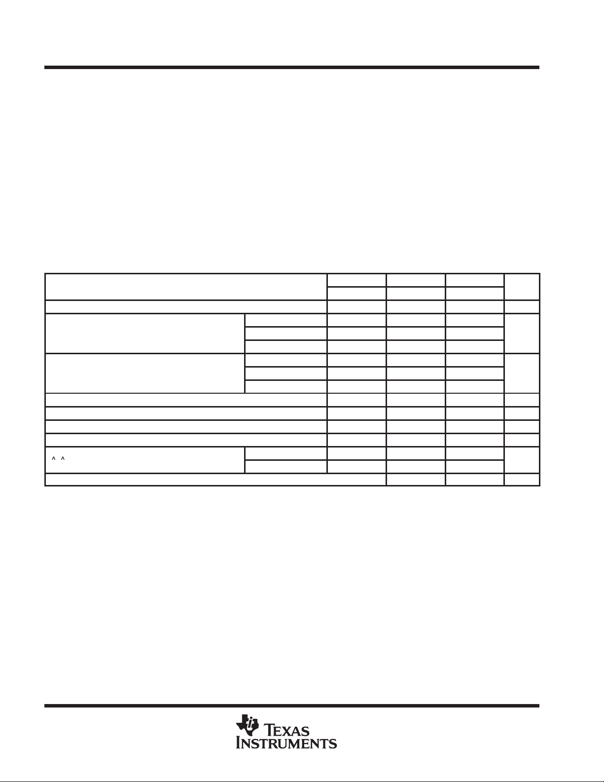
recommended operating conditions (see Note 4)
TA = 25°C CD54AC163 CD74AC163
MIN MAX MIN MAX MIN MAX
V
V
V
V
V
I
OH
I
OL
T
NOTE 4: All unused inputs of the device must be held at VCC or GND to ensure proper device operation. Refer to the TI application report,
Supply voltage 1.5 5.5 1.5 5.5 1.5 5.5 V
CC
VCC = 1.5 V 1.2 1.2 1.2
High-level input voltage
IH
Low-level input voltage
IL
Input voltage 0 V
I
Output voltage 0 V
O
High-level output current –24 –24 –24 mA
Low-level output current 24 24 24 mA
p
Operating free-air temperature –55 125 –40 85 °C
A
Implications of Slow or Floating CMOS Inputs
VCC = 3 V
VCC = 5.5 V 3.85 3.85 3.85
VCC = 1.5 V 0.3 0.3 0.3
VCC = 3 V
VCC = 5.5 V 1.65 1.65 1.65
VCC = 1.5 V to 3 V 0 50 0 50 0 50
VCC = 3.6 V to 5.5 V 0 20 0 20 0 20
, literature number SCBA004.
2.1 2.1 2.1
0.9 0.9 0.9
CC
CC
0 V
0 V
CC
CC
0 V
0 V
CC
CC
V
V
V
V
6
POST OFFICE BOX 655303 • DALLAS, TEXAS 75265
Page 7

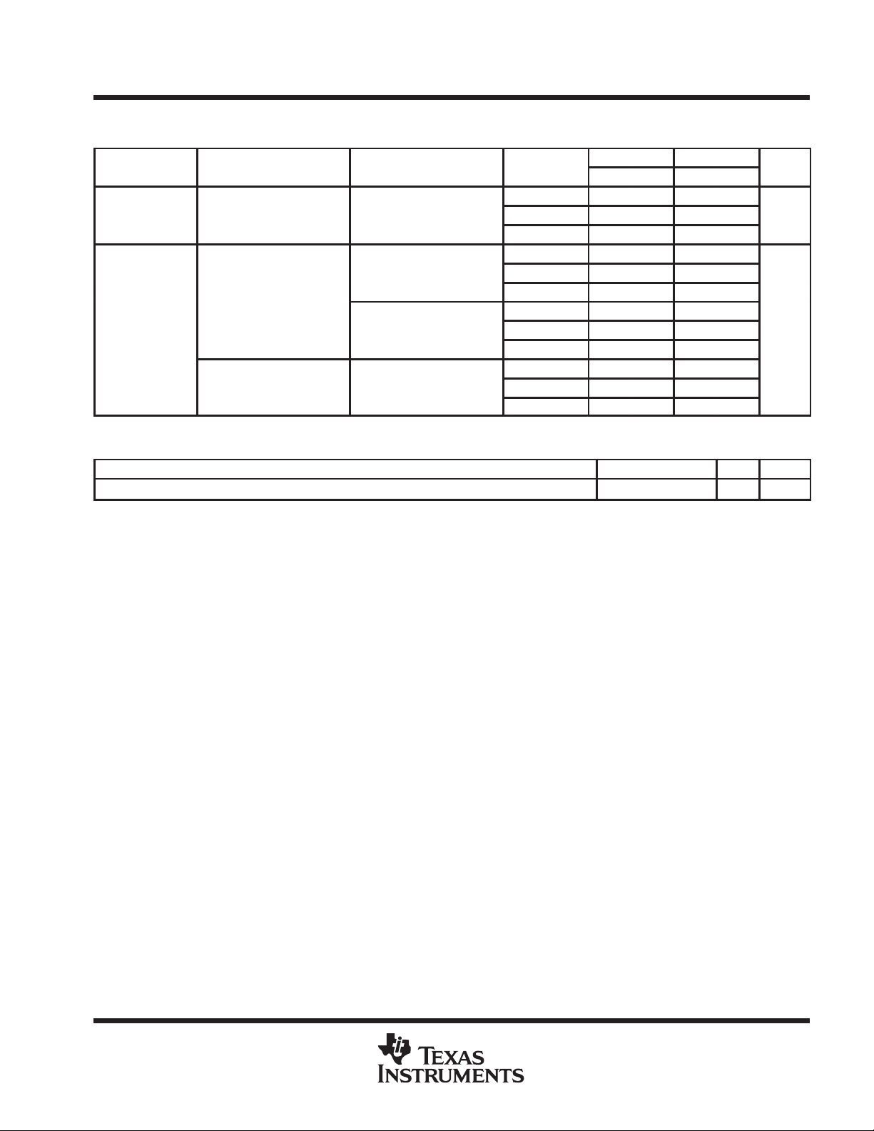
PARAMETER
TEST CONDITIONS
V
UNIT
CD54AC163, CD74AC163
4-BIT SYNCHRONOUS BINARY COUNTERS
SCHS299 – APRIL 2000
electrical characteristics over recommended operating free-air temperature range (unless
otherwise noted)
CC
1.5 V 1.4 1.4 1.4
IOH = –50 µA
V
OH
V
OL
I
I
I
CC
C
†
i
T est one output at a time, not exceeding 1-second duration. Measurement is made by forcing indicated current and measuring voltage to minimize
power dissipation. T est verifies a minimum 50-Ω transmission-line drive capability at 85°C and 75-Ω transmission-line drive capability at 125°C.
VI = VIH or V
VI = VIH or V
VI = VCC or GND 5.5 V ±0.1 ±1 ±1 µA
VI = VCC or GND, IO = 0 5.5 V 8 160 80 µA
IL
IL
IOH = –4 mA 3 V 2.58 2.4 2.48
IOH = –24 mA 4.5 V 3.94 3.7 3.8
IOH = –50 mA
IOH = –75 mA
IOL = 50 µA
IOL = 12 mA 3 V 0.36 0.5 0.44
IOL = 24 mA 4.5 V 0.36 0.5 0.44
IOL = 50 mA
IOL = 75 mA
†
†
†
†
3 V 2.9 2.9 2.9
4.5 V 4.4 4.4 4.4
5.5 V – 3.85 –
5.5 V – – 3.85
1.5 V 0.1 0.1 0.1
3 V 0.1 0.1 0.1
4.5 V 0.1 0.1 0.1
5.5 V – 1.65 –
5.5 V – – 1.65
TA = 25°C CD54AC163 CD74AC163
MIN MAX MIN MAX MIN MAX
V
V
10 10 10 pF
POST OFFICE BOX 655303 • DALLAS, TEXAS 75265
7
Page 8

CD54AC163, CD74AC163
V
UNIT
tsuSetup time, before CLK↑
ns
thHold time, after CLK↑
ns
4-BIT SYNCHRONOUS BINARY COUNTERS
SCHS299 – APRIL 2000
timing requirements over recommended operating free-air temperature range (unless otherwise
noted)
CD54AC163 CD74AC163
MIN MAX MIN MAX
64 73
MHz
ns
f
clock
t
w
Clock frequency
Pulse duration CLK high or low
A, B, C, or D
ENP or ENT
p
LOAD low
CLR inactive
A, B, C, or D
ENP or ENT
LOAD low
CLR inactive
CC
1.5 V 7 8
3.3 V ± 0.3 V
5 V ± 0.5 V 90 103
1.5 V 69 61
3.3 V ± 0.3 V 7.7 6.8
5 V ± 0.5 V 5.5 4.8
1.5 V 63 55
3.3 V ± 0.3 V 7 6.1
5 V ± 0.5 V 5 4.4
1.5 V 63 55
3.3 V ± 0.3 V 9.6 8.2
5 V ± 0.5 V 5 4.4
1.5 V 75 66
3.3 V ± 0.3 V 8.4 7.4
5 V ± 0.5 V 6 5.3
1.5 V 75 66
3.3 V ± 0.3 V 8.4 7.4
5 V ± 0.5 V 6 5.3
1.5 V 0 0
3.3 V ± 0.3 V 0 0
5 V ± 0.5 V 0 0
1.5 V 0 0
3.3 V ± 0.3 V 0 0
5 V ± 0.5 V 0 0
1.5 V 0 0
3.3 V ± 0.3 V 0 0
5 V ± 0.5 V 0 0
1.5 V 0 0
3.3 V ± 0.3 V 0 0
5 V ± 0.5 V 0 0
8
POST OFFICE BOX 655303 • DALLAS, TEXAS 75265
Page 9
PARAMETER
V
UNIT
CLK
CD54AC163, CD74AC163
4-BIT SYNCHRONOUS BINARY COUNTERS
SCHS299 – APRIL 2000
switching characteristics over recommended operating free-air temperature range, CL = 50 pF
(unless otherwise noted) (see Figure 1)
FROM TO
(INPUT) (OUTPUT)
f
max
t
pd
ENT RCO
operating characteristics, TA = 25°C
PARAMETER TEST CONDITIONS TYP UNIT
C
Power dissipation capacitance No load 66 pF
pd
RCO
Any Q
CC
1.5 V 7 8
3.3 V ± 0.3 V 64 73
5 V ± 0.5 V 90 103
1.5 V – 209 – 190
3.3 V ± 0.3 V 6 23.4 6 21
5 V ± 0.5 V 4.3 16.7 4.3 15.2
1.5 V – 207 – 188
3.3 V ± 0.3 V 5.9 23.1 5.9 21
5 V ± 0.5 V 4.2 16.5 4.2 15
1.5 V – 129 – 117
3.3 V ± 0.3 V 3.6 14.4 3.7 13.1
5 V ± 0.5 V 2.6 10.3 2.7 9.4
CD54AC163 CD74AC163
MIN MAX MIN MAX
MHz
ns
POST OFFICE BOX 655303 • DALLAS, TEXAS 75265
9
Page 10

CD54AC163, CD74AC163
4-BIT SYNCHRONOUS BINARY COUNTERS
SCHS299 – APRIL 2000
PARAMETER MEASUREMENT INFORMATION
From Output
Under Test
CL = 50 pF
(see Note A)
NOTE When VCC = 1.5 V, R1 and R2 = 1 kΩ.
LOAD CIRCUIT
R1 = 500 Ω
R2 = 500 Ω
S1
2 × V
Open
GND
CC
Input
TEST S1
t
PLH/tPHL
t
PLZ/tPZL
t
PHZ/tPZH
t
w
50% V
CC
VOLTAGE WAVEFORMS
PULSE DURATION
Open
2 × V
GND
CC
50% V
CC
V
0 V
CC
CLR
Input
CLK
VOLTAGE WAVEFORMS
RECOVERY TIME
Input
In-Phase
Output
Out-of-Phase
Output
PROPAGATION DELAY AND OUTPUT TRANSITION TIMES
50% V
CC
t
PLH
50%
t
PHL
VOLTAGE WAVEFORMS
50% V
CC
50% V
50% V
t
PHL
90% 90%
t
r
t
PLH
50% V
CC
10% 10%
t
f
t
rec
CC
50%
CC
V
0 V
V
0 V
50% V
10%10%
90%90%
CC
CC
t
t
CC
f
r
Reference
Input
t
su
Data
50%
Input
SETUP AND HOLD AND INPUT RISE AND FALL TIMES
V
CC
0 V
V
V
V
V
OH
OL
OH
OL
Output
Control
Output
Waveform 1
S1 at 2 × V
(see Note B)
Output
Waveform 2
S1 at Open
(see Note B)
90% 90%
VOLTAGE WAVEFORMS
t
PZL
CC
t
PZH
OUTPUT ENABLE AND DISABLE TIMES
50% V
CC
t
h
t
r
50% V
CC
50% V
CC
50% V
CC
VOLTAGE WAVEFORMS
50% V
10%10%
50% V
t
VOL + 0.3 V
t
VOH – 0.3 V
CC
PLZ
PHZ
V
CC
0 V
V
CC
CC
0 V
t
f
V
CC
0 V
[
V
CC
V
OL
V
OH
[
0 V
NOTES: A. CL includes probe and test-fixture capacitance.
B. Waveform 1 is for an output with internal conditions such that the output is low except when disabled by the output control.
Waveform 2 is for an output with internal conditions such that the output is high except when disabled by the output control.
C. All input pulses are supplied by generators having the following characteristics: PRR ≤ 1 MHz, ZO = 50 Ω, tr = 3 ns, tf = 3 ns.
Phase relationships between waveforms are arbitrary.
D. For clock inputs, f
E. The outputs are measured one at a time with one input transition per measurement.
F. t
G. t
H. t
PLH
PZL
PLZ
and t
and t
and t
PHL
PZH
PHZ
is measured with the input duty cycle at 50%.
max
are the same as tpd.
are the same as ten.
are the same as t
dis
.
Figure 1. Load Circuit and Voltage Waveforms
10
POST OFFICE BOX 655303 • DALLAS, TEXAS 75265
Page 11

IMPORTANT NOTICE
T exas Instruments and its subsidiaries (TI) reserve the right to make changes to their products or to discontinue
any product or service without notice, and advise customers to obtain the latest version of relevant information
to verify, before placing orders, that information being relied on is current and complete. All products are sold
subject to the terms and conditions of sale supplied at the time of order acknowledgment, including those
pertaining to warranty, patent infringement, and limitation of liability.
TI warrants performance of its semiconductor products to the specifications applicable at the time of sale in
accordance with TI’s standard warranty. Testing and other quality control techniques are utilized to the extent
TI deems necessary to support this warranty . Specific testing of all parameters of each device is not necessarily
performed, except those mandated by government requirements.
Customers are responsible for their applications using TI components.
In order to minimize risks associated with the customer’s applications, adequate design and operating
safeguards must be provided by the customer to minimize inherent or procedural hazards.
TI assumes no liability for applications assistance or customer product design. TI does not warrant or represent
that any license, either express or implied, is granted under any patent right, copyright, mask work right, or other
intellectual property right of TI covering or relating to any combination, machine, or process in which such
semiconductor products or services might be or are used. TI’s publication of information regarding any third
party’s products or services does not constitute TI’s approval, warranty or endorsement thereof.
Copyright 2000, Texas Instruments Incorporated
 Loading...