

Datasheet CD4541BPWR, CD4541BM96, CD4541BM, CD4541BF3A, CD4541BF Datasheet (Texas Instruments)
...
CD4541B
/
j
/
/
[ /Title
(CD45
41B)
Sub-
ect
(CMO
S Programmable
Timer
High
Voltage
Types
(20V
Rating))
Autho
r ()
Keywords
(Harris
Semiconductor,
CD400
0,
metal
gate,
CMOS
, pdip,
cerdip,
mil,
military,
mil
Data sheet acquired from Harris Semiconductor
SCHS085
Features
• Low Symmetrical Output Resistance, Typically 100Ω
at V
= 15V
DD
• Built-In Low-Power RC Oscillator
• Oscillator Frequency Range. . . . . . . . . . DC to 100kHz
• External Clock (Applied to Pin 3) can be Used Instead
of Oscillator
N
• Operates as 2
Transition Timer
Q Select Provides Output Logic Level Flexibility
•Q/
• AUTO or MASTER RESET Disables Oscillator During
Reset to Reduce Power Dissipation
• Operates With Very Slow Clock Rise and Fall Times
• Capable of Driving Six Low Power TTL Loads, Three
Low-Power Schottky Loads, or Six HTL Loads Over
the Rated Temperature Range
• Symmetrical Output Characteristics
• 100% Tested for Quiescent Current at 20V
• 5V, 10V, and 15V Parametric Ratings
• Meets All Requirements of JEDEC Standard No. 13B,
“Standard Specifications for Description of ‘B’ Series
CMOS Devices”
Frequency Divider or as a Single-
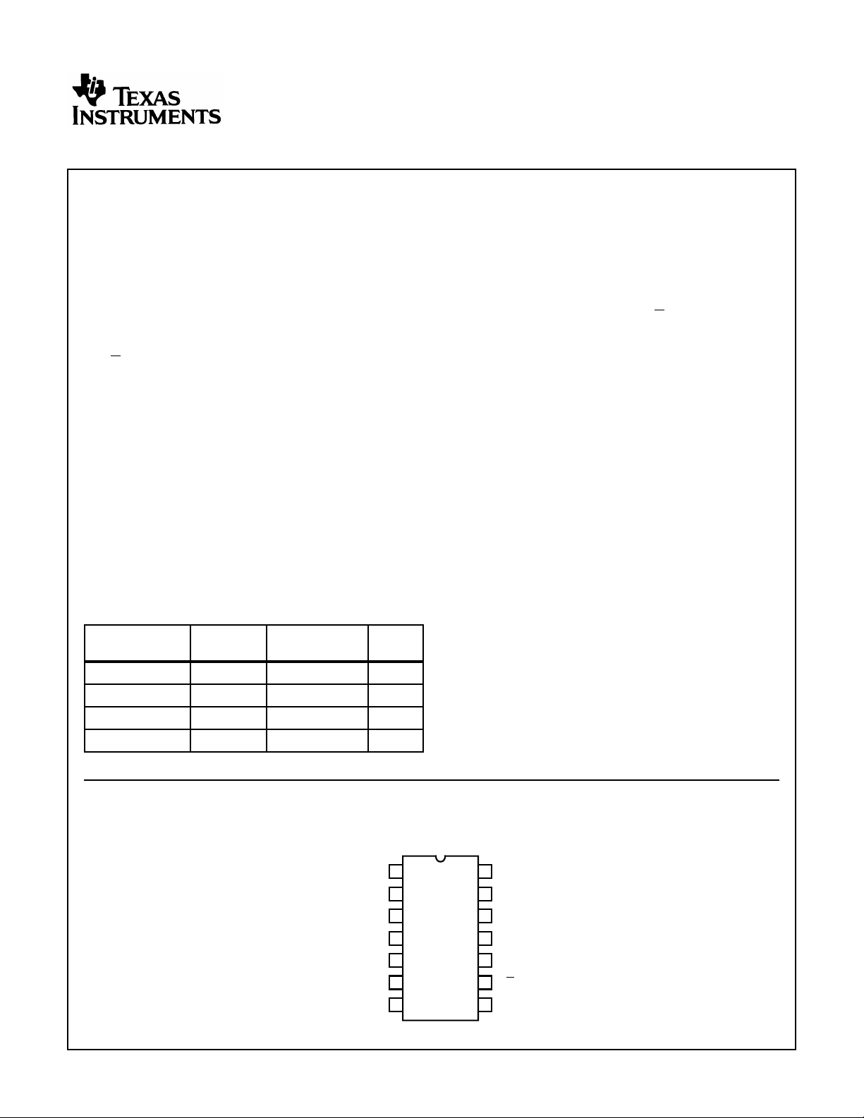
Ordering Information
TEMP.
PART NUMBER
CD4541BF -55 to 125 14 Ld CERDIP F14.3
CD4541BE -55 to 125 14 Ld PDIP E14.3
CD4541BH -55 to 125 Chip CD4541BM -55 to 125 14 Ld SOIC M14.15
RANGE (oC) PACKAGE
Pinout
CD4541B (CERDIP, PDIP, SOIC)
R
TC
C
TC
R
NC
AUTO RESET
MASTER RESET
V
SS
PKG.
NO.
S
1
2
3
4
5
6
7
CMOS Programmable Timer
High Voltage Types (20V Rating)
Description
CD4541B programmable timer consists of a 16-stage binary
counter, an oscillator that is controlled by external R-C components (2 resistors and a capacitor), an automatic power-on
reset circuit, and output control logic. The counter increments
on positive-edge clock transitions and can also be reset via the
MASTER RESET input.
The output from this timer is the Q or
10th, 13th, or 16th counter stage. The desired stage is chosen
using time-select inputs A and B (see Frequency Select Table).
The output is available in either of two modes selectable via the
MODE input, pin 10 (see TruthTable). When this MODE input is
a logic “1”, the output will be a continuous square wave having
a frequency equal to the oscillator frequency divided by 2
With the MODE input set to logic “0” and after a MASTER
RESET is initiated, the output (assuming Q output has been
selected) changes from a low to a high state after 2
and remains in that state until another MASTER RESET pulse
is applied or the MODE input is set to a logic “1”.
Timing is initialized by setting the AUTO RESET input (pin 5) to
logic “0” and turning power on. If pin 5 is set to logic “1”, the
AUT ORESET circuit is disabled and counting will not start until
after a positive MASTER RESET pulse is applied and returns
to a low level. The AUTO RESET consumes an appreciable
amount of power and should not be used if low-power operation
is desired. For reliable automatic power-on reset, V
be greater than 5V.
The RC oscillator, shown in Figure 2, oscillates with a
frequency determined by the RC network and is calculated
using:
f =
TOP VIEW
1
---------------------------------- -
2.3 R
TCCTC
V
14
DD
B
13
12
A
11
NC
10
MODE
9
Q/
8
OUTPUT
Where f is between 1kHz
and 100kHz
and R
S
Q SELECT
10k≥Ωand 2RTC≈
Q output from the 8th,
N-1
DD
N
counts
should
.
CAUTION: These devices are sensitive to electrostatic discharge. Users should follow proper IC Handling Procedures.
Copyright
© Harris Corporation 1998
1
File Number 1378.1
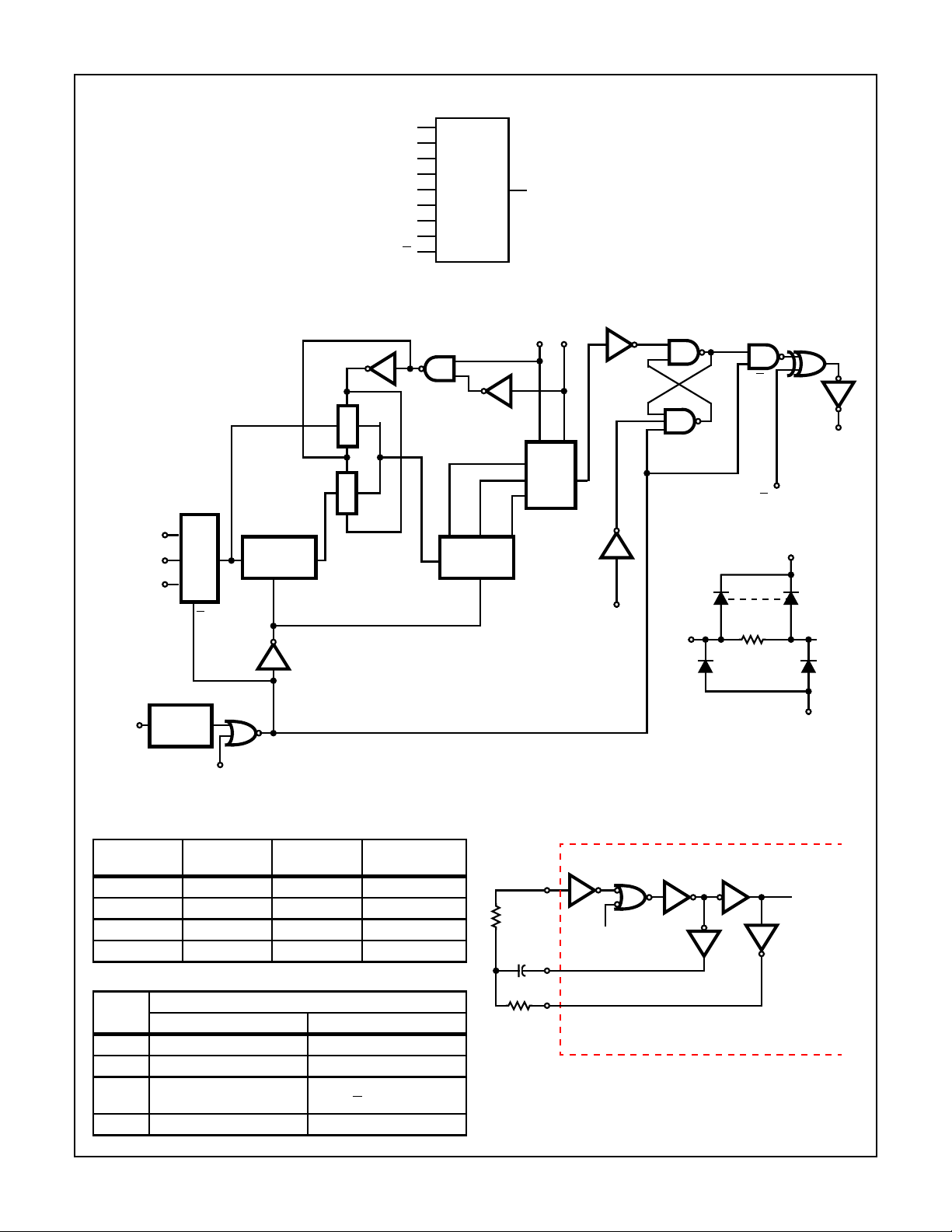
Functional Diagram
R
TC
C
TC
R
AR
MR
MODE
Q/
SELECT
CD4541B
12
A
13
B
1
2
3
S
5
6
10
9
Q
8
V
DD
V
SS
Q
= PIN 14
= PIN 7
Functional Block Diagram
3
†R
S
2
†C
TC
1
†R
TC
5
PWR ON
RESET
AUTO
RESET†
MANUAL RESET†
OSC
R
8-STAGE
COUNTER
R
6
N
P
N
P
V
= 14
DD
V
= 7 NC = 4, 11
SS
2102
8-STAGE
COUNTER
FIGURE 1.
12 13
†A †B
R
8
Q
1 OF 3
MUX
16
2
OR
13
8
2
R
10
†Q/Q SELECT
9
V
DD
†MODE
V
SS
† All inputs are protected by CMOS Protection Network.
FREQUENCY SELECTION TABLE
NO. OF
AB
STAGES N COUNT 2
N
0 0 13 8192
0 1 10 1024
108256
1 1 16 65536
TRUTH TABLE
STATE
PIN
01
5 Auto Reset On Auto Reset Disable
6 Master Reset Off Master Reset On
9 Output Initially Low After
Reset (Q)
Output Initially High After
Q)
Reset (
10 Single Transition Mode Recycle Mode
3
R
S
C
TC
R
TC
2
1
INTERNAL
RESET
TO CLOCK
CKT
FIGURE 2. RC OSCILLATOR CIRCUIT
2
CD4541B
Absolute Maximum Ratings Thermal Information
DC Supply - Voltage Range, V
Voltages Referenced to VSSTerminal . . . . . . . . . . -0.5V to +20V
Input Voltage Range, All Inputs . . . . . . . . . . . . . -0.5V to VDD+0.5V
DC Input Current, Any One Input . . . . . . . . . . . . . . . . . . . . . ±10mA
Device Dissipation Per Output Transistor
For TA = Full Package Temperature Range
(All Package Types) . . . . . . . . . . . . . . . . . . . . . . . . . . . . . 100mW
DD
Operating Conditions
Temperature Range TA. . . . . . . . . . . . . . . . . . . . . . . -55oC to 125oC
Supply Voltage Range
For TA = Full Package Temperature Range . . . . .3V (Min), 18V (Typ)
CAUTION: Stresses above those listed in “Absolute Maximum Ratings” may cause permanent damage to the device. This is a stress only rating and operation
of the device at these or any other conditions above those indicated in the operational sections of this specification is not implied.
NOTE:
1. θJA is measured with the component mounted on an evaluation PC board in free air.
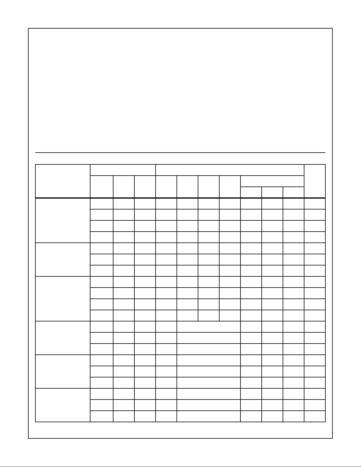
Electrical Specifications
CONDITIONS LIMITS AT INDICATED TEMPERATURES (oC)
Thermal Resistance (Typical, Note 1) θJA (oC/W) θJC (oC/W)
PDIP Package. . . . . . . . . . . . . . . . . . . 90 N/A
CERDIP Package . . . . . . . . . . . . . . . . 90 36
SOIC Package. . . . . . . . . . . . . . . . . . . 120 N/A
Maximum Junction Temperature (Plastic Package) . . . . . . . . 150oC
Maximum Storage Temperature Range (T
Maximum Lead Temperature (Soldering 10s)
At Distance 1/16in ± 1/32in (1.59mm ±0.79mm)
from case for 10s Maximum . . . . . . . . . . . . . . . . . . . . . . . . 265oC
(SOIC - Lead Tips Only)
) . . . -65oC to 150oC
STG
PARAMETER
Quiescent Device
Current,
(Note 2) IDD (Max)
Output Low (Sink)
Current lOL(Min)
Output High (Source)
Current, IOH (Min)
Output Voltage:
Low-Level, VOL (Max)
V
O
(V)
- 0, 5 5 5 5 150 150 - 0.04 5 µA
- 0, 10 10 10 10 300 300 - 0.04 10 µA
- 0, 15 15 20 20 600 600 - 0.04 20 µA
- 0, 20 20 100 100 3000 3000 - 0.08 100 µA
0.4 0, 5 5 1.9 1.85 1.26 1.08 1.55 3.1 - µA
0.5 0, 10 10 5 4.8 3.3 2.8 4 8 - µA
1.5 0, 15 15 12.6 12 8.4 7.2 10 20 - µA
4.6 0, 5 5 -1.9 -1.85 -1.26 -1.08 -1.55 -3.1 - mA
2.5 0, 5 5 -6.2 -6 -4.1 -3 -5 -10 - mA
9.5 0, 10 10 -5 -4.8 -3.3 -2.8 -4 -8 - mA
13.5 0, 15 15 -12.6 -12 -8.4 -7.2 -10 -20 - mA
- 0, 5 5 - 0.05 - 0 0.05 mA
- 0, 10 10 - 0.05 - 0 0.05 mA
- 0, 15 15 - 0.05 - 0 0.05 mA
V
(V)
V
IN
DD
(V) -55 -40 85 125
MIN TYP MAX
25
UNITS
Output Voltage:
High-Level, VOH (Min)
Input Low Voltage,
VIL (Max)
- 0, 5 5 - 4.95 4.95 5 - mA
- 0, 10 10 - 9.95 9.95 10 - mA
- 0, 15 15 - 14.95 14.95 15 - mA
0.5, 4.5 - 5 - 1.5 - - 1.5 V
1, 9 - 10 - 3 - - 3 V
1.5, 13.5 - 15 - 4 - - 4 V
3

Electrical Specifications (Continued)
CONDITIONS LIMITS AT INDICATED TEMPERATURES (oC)
CD4541B
PARAMETER
Input High Voltage,
V
O
(V)
0.5, 4.5 - 5 - 3.5 3.5 - - V
V
(V)
V
IN
DD
(V) -55 -40 85 125
MIN TYP MAX
VIH(Min)
1, 9 - 10 - 7 7 - - V
1.5, 13.5 - 15 - 11 11 - - V
Input Current, lIN (Max) - 0, 18 18 ±0.1 ±0.1 ±1 ±1-±10
NOTE:
2. With AUTO RESET enabled, additional current drain at 25oC is:
7µA (Typ), 200µA (Max) at 5V;
30µA (Typ), 350µA (Max) at 10V;
80µA (Typ), 500µA (Max) at 15V
Dynamic Electrical Specifications T
= 25oC, Input tr, tf = 20ns, CL = 50pF, RL = 200kΩ
A
PARAMETER SYMBOL VDD (V) MIN TYP MAX UNITS
Propagation Delay Times
(28) t
PHL
, t
PLH
5 - 3.5 10.5 µs
Clock to Q
10 - 1.25 3.8 µs
15 - 0.9 2.9 µs
(216) t
PHL
, t
PLH
5 - 6.0 18 µs
10 - 3.5 10 µs
25
-5
UNITS
±0.1 µA
Transition Time t
MASTER RESET, CLOCK
Pulse Width
Maximum Clock Pulse Input
Frequency
Maximum Clock Pulse Input
Rise or Fall time
THL
t
THL
f
tr,t
CL
15 - 2.5 7.5 µs
5 - 100 200 ns
10 - 50 100 ns
15 - 40 80 ns
5 - 180 360 ns
10 - 90 180 ns
15 - 65 130 ns
5 900 300 - ns
10 300 100 - ns
15 225 85 - ns
5 - 1.5 - MHz
10 - 4 - MHz
15 - 6 - MHz
f
5, 10, 15 Unlimited µs
4

CD4541B
Digital Timer Application
A positive pulse on MASTER RESET resets the counters
and latch. The output goes high and remains high until the
number of pulses, selected by A and B, are counted. This
circuit is retriggerable and is as accurate as the input frequency. If additional accuracy is desired, an external clock
can be used on pin 3. A setup time equal to the width of the
one-shot output is required immediately following initial
power up, during which time the output will be high.
V
R
INPUT
TC
C
TC
RSAR
MR
1
2
3
4
5
6
7
14
13
12
11
10
9
8
OUTPUT
FIGURE 3. DIGITAL TIMER APPLICATION CIRCUIT
DD
B
A
t
0102030405060708088
82
80
70
60
50
79 - 87
40
30
20
10
0
4 - 10
(0.102 - 0.254)
85 - 93
(2.159 - 2.362)
(2.007 - 2.210)
NOTE: Dimensions in parentheses are in millimeters and are derived from the basic inch dimensions as indicated. Grid graduations
are in mils (10-3 inch).
FIGURE 4. DIMENSIONS AND PAD LAYOUT FOR CD4541B
5

Dual-In-Line Plastic Packages (PDIP)
CD4541B
N
D1
-C-
E1
-B-
A1
A2
E
A
L
e
C
C
L
e
A
C
e
B
INDEX
AREA
BASE
PLANE
SEATING
PLANE
D1
B1
1 2 3 N/2
-AD
e
B
0.010 (0.25) C AM BS
NOTES:
1. Controlling Dimensions: INCH. In case of conflict between English
and Metric dimensions, the inch dimensions control.
2. Dimensioning and tolerancing per ANSI Y14.5M-1982.
3. Symbols are defined in the “MO SeriesSymbolList”in Section 2.2 of
Publication No. 95.
4. Dimensions A, A1 and L are measured with the package seated in
JEDEC seating plane gauge GS-3.
5. D, D1, and E1 dimensions do not include mold flash or protrusions.
Mold flash or protrusions shall not exceed 0.010 inch (0.25mm).
6. E and are measured with the leads constrained to be perpen-
e
dicular to datum .
A
-C-
7. eB and eC are measured at the lead tips with the leads unconstrained. eC must be zero or greater.
8. B1maximum dimensionsdonotincludedambar protrusions.Dambar
protrusions shall not exceed 0.010 inch (0.25mm).
9. N is the maximum number of terminal positions.
10. Corner leads (1, N, N/2 and N/2 + 1) for E8.3, E16.3, E18.3, E28.3,
E42.6 will have a B1 dimension of 0.030 - 0.045 inch (0.76 -
1.14mm).
E14.3 (JEDEC MS-001-AA ISSUE D)
14 LEAD DUAL-IN-LINE PLASTIC PACKAGE
INCHES MILLIMETERS
SYMBOL
A - 0.210 - 5.33 4
A1 0.015 - 0.39 - 4
A2 0.115 0.195 2.93 4.95 -
B 0.014 0.022 0.356 0.558 B1 0.045 0.070 1.15 1.77 8
C 0.008 0.014 0.204 0.355 -
D 0.735 0.775 18.66 19.68 5
D1 0.005 - 0.13 - 5
E 0.300 0.325 7.62 8.25 6
E1 0.240 0.280 6.10 7.11 5
e 0.100 BSC 2.54 BSC -
e
A
e
B
0.300 BSC 7.62 BSC 6
- 0.430 - 10.92 7
L 0.115 0.150 2.93 3.81 4
N14 149
NOTESMIN MAX MIN MAX
Rev. 0 12/93
6

CD4541B
Ceramic Dual-In-Line Frit Seal Packages (CERDIP)
LEAD FINISH
c1
-DBASE
M
SECTION A-A
METAL
b1
M
(b)
α
E
D
S
S
Q
A
-CL
eA
eA/2
aaa C A - B
M
c
D
S S
bbb C A - B
BASE
PLANE
SEATING
PLANE
S1
b2
b
ccc C A - BMD
-A-
-B-
S
D
A
A
e
S
S
NOTES:
1. Index area: A notch orapinoneidentificationmarkshallbelocated adjacent to pin one and shall be located within the shaded
area shown. The manufacturer’s identification shall not be used
as a pin one identification mark.
2. The maximum limits of lead dimensions b and c or M shall be
measured at the centroid of the finished lead surfaces, when
solder dip or tin plate lead finish is applied.
3. Dimensions b1 and c1 apply to lead base metal only. Dimension
M applies to lead plating and finish thickness.
4. Corner leads (1, N, N/2, and N/2+1) may be configured with a
partial lead paddle. For this configuration dimension b3 replaces
dimension b2.
5. This dimension allows for off-center lid, meniscus, and glass
overrun.
6. Dimension Q shall be measured from the seating plane to the
base plane.
7. Measure dimension S1 at all four corners.
8. N is the maximum number of terminal positions.
9. Dimensioning and tolerancing per ANSI Y14.5M - 1982.
10. Controlling dimension: INCH.
F14.3 MIL-STD-1835 GDIP1-T14 (D-1, CONFIGURATION A)
14 LEAD CERAMIC DUAL-IN-LINE FRIT SEAL PACKAGE
(c)
SYMBOL
A - 0.200 - 5.08 -
b 0.014 0.026 0.36 0.66 2
b1 0.014 0.023 0.36 0.58 3
b2 0.045 0.065 1.14 1.65 b3 0.023 0.045 0.58 1.14 4
c 0.008 0.018 0.20 0.46 2
c1 0.008 0.015 0.20 0.38 3
D - 0.785 - 19.94 5
E 0.220 0.310 5.59 7.87 5
e 0.100 BSC 2.54 BSC eA 0.300 BSC 7.62 BSC -
eA/2 0.150 BSC 3.81 BSC -
L 0.125 0.200 3.18 5.08 -
Q 0.015 0.060 0.38 1.52 6
S1 0.005 - 0.13 - 7
α
aaa - 0.015 - 0.38 bbb - 0.030 - 0.76 ccc - 0.010 - 0.25 -
M - 0.0015 - 0.038 2, 3
N14 148
INCHES MILLIMETERS
90
o
105
o
90
o
105
NOTESMIN MAX MIN MAX
o
Rev. 0 4/94
-
7

Small Outline Plastic Packages (SOIC)
CD4541B
N
INDEX
AREA
123
-A-
E
-B-
SEATING PLANE
D
A
-C-
0.25(0.010) BM M
H
L
h x 45
o
α
e
B
0.25(0.010) C AM BS
M
NOTES:
1. Symbols are defined in the “MO Series Symbol List” in Section 2.2 of
Publication Number 95.
2. Dimensioning and tolerancing per ANSI Y14.5M-1982.
3. Dimension “D” does not include mold flash, protrusions or gate burrs.
Mold flash, protrusion and gate burrs shall not exceed0.15mm (0.006
inch) per side.
4. Dimension“E” doesnotinclude interleadflashor protrusions.Interlead
flash and protrusions shall not exceed 0.25mm (0.010 inch) per side.
5. The chamfer on the body is optional. If it is not present, avisual index
feature must be located within the crosshatched area.
6. “L” is the length of terminal for soldering to a substrate.
7. “N” is the number of terminal positions.
8. Terminal numbers are shown for reference only.
9. The lead width “B”, as measured 0.36mm (0.014 inch) or greater
above the seating plane, shall not exceed a maximum value of
0.61mm (0.024 inch).
10. Controlling dimension: MILLIMETER. Converted inchdimensions
are not necessarily exact.
A1
C
0.10(0.004)
M14.15 (JEDEC MS-012-AB ISSUE C)
14 LEAD NARROW BODY SMALL OUTLINE PLASTIC
PACKAGE
INCHES MILLIMETERS
SYMBOL
A 0.0532 0.0688 1.35 1.75 -
A1 0.0040 0.0098 0.10 0.25 -
B 0.013 0.020 0.33 0.51 9
C 0.0075 0.0098 0.19 0.25 D 0.3367 0.3444 8.55 8.75 3
E 0.1497 0.1574 3.80 4.00 4
e 0.050 BSC 1.27 BSC -
H 0.2284 0.2440 5.80 6.20 -
h 0.0099 0.0196 0.25 0.50 5
L 0.016 0.050 0.40 1.27 6
N14 147
o
α
0
o
8
o
0
o
8
Rev. 0 12/93
NOTESMIN MAX MIN MAX
-
8

IMPORTANT NOTICE
T exas Instruments and its subsidiaries (TI) reserve the right to make changes to their products or to discontinue
any product or service without notice, and advise customers to obtain the latest version of relevant information
to verify, before placing orders, that information being relied on is current and complete. All products are sold
subject to the terms and conditions of sale supplied at the time of order acknowledgement, including those
pertaining to warranty, patent infringement, and limitation of liability.
TI warrants performance of its semiconductor products to the specifications applicable at the time of sale in
accordance with TI’s standard warranty. Testing and other quality control techniques are utilized to the extent
TI deems necessary to support this warranty . Specific testing of all parameters of each device is not necessarily
performed, except those mandated by government requirements.
CERTAIN APPLICATIONS USING SEMICONDUCTOR PRODUCTS MAY INVOLVE POTENTIAL RISKS OF
DEATH, PERSONAL INJURY, OR SEVERE PROPERTY OR ENVIRONMENTAL DAMAGE (“CRITICAL
APPLICATIONS”). TI SEMICONDUCTOR PRODUCTS ARE NOT DESIGNED, AUTHORIZED, OR
WARRANTED TO BE SUITABLE FOR USE IN LIFE-SUPPORT DEVICES OR SYSTEMS OR OTHER
CRITICAL APPLICA TIONS. INCLUSION OF TI PRODUCTS IN SUCH APPLICATIONS IS UNDERST OOD TO
BE FULLY AT THE CUSTOMER’S RISK.
In order to minimize risks associated with the customer’s applications, adequate design and operating
safeguards must be provided by the customer to minimize inherent or procedural hazards.
TI assumes no liability for applications assistance or customer product design. TI does not warrant or represent
that any license, either express or implied, is granted under any patent right, copyright, mask work right, or other
intellectual property right of TI covering or relating to any combination, machine, or process in which such
semiconductor products or services might be or are used. TI’s publication of information regarding any third
party’s products or services does not constitute TI’s approval, warranty or endorsement thereof.
Copyright 1998, Texas Instruments Incorporated
 Loading...