

Page 1
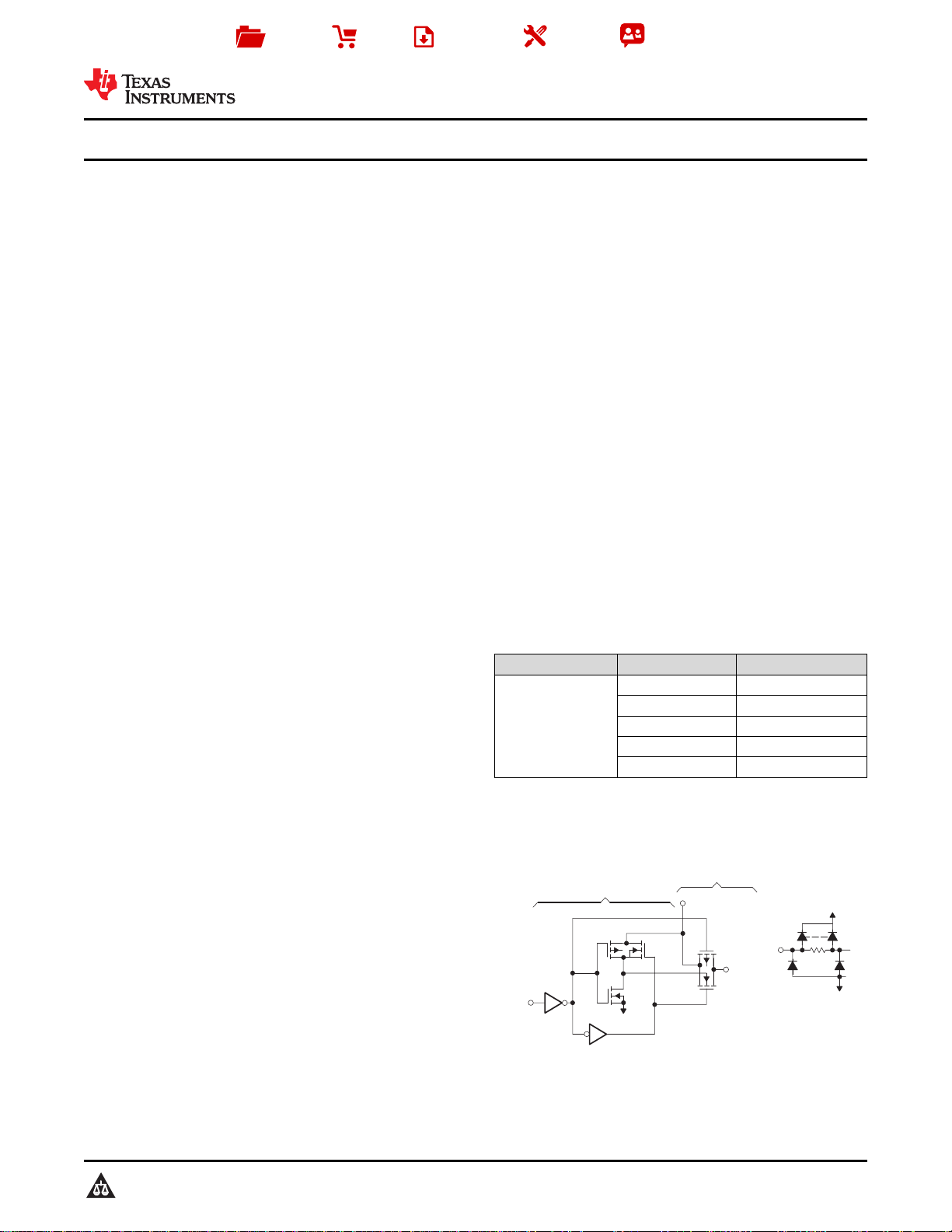
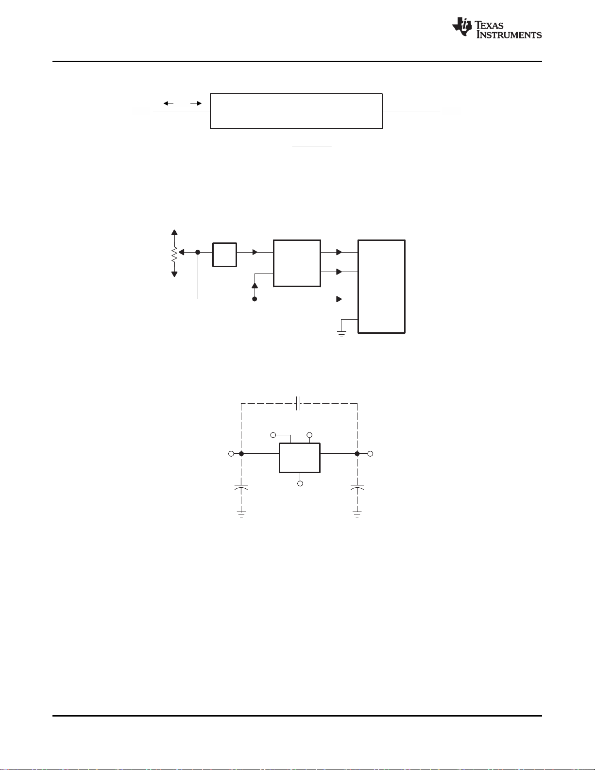
Control
V
C
(1)
V
DD
V
SS
V
SS
n
n
p
Out
V
os
Control
Switch
In
n
p
V
is
CMOS Protection Network
Copyright © 2016, Texas Instruments Incorporated
Product
Folder
Order
Now
Technical
Documents
Tools &
Software
Support &
Community
SCHS051H –NOVEMBER 1998–REVISED FEBRUARY 2020
CD4066B CMOS Quad Bilateral Switch
CD4066B
1 Features
1
• 15-V Digital or ±7.5-V Peak-to-Peak Switching
• 125-Ω Typical On-State Resistance for
15-V Operation
• Switch On-State Resistance Matched to Within
5 Ω Over 15-V Signal-Input Range
• On-State Resistance Flat Over Full
Peak-to-Peak Signal Range
• High On or Off Output-Voltage Ratio:
80 dB Typical at fis= 10 kHz, RL= 1 kΩ
• High Degree of Linearity: <0.5% Distortion Typical
at fis= 1 kHz, Vis= 5-V
p-p
VDD– VSS≥ 10-V, RL= 10 kΩ
• Extremely Low Off-State Switch Leakage,
Resulting in Very Low Offset Current and High
Effective Off-State Resistance: 10 pA Typical at
VDD– VSS= 10-V, TA= 25°C
• Extremely High Control Input Impedance
(Control Circuit Isolated From Signal Circuit):
1012Ω Typical
• Low Crosstalk Between Switches: –50 dB Typical
at fis= 8 MHz, RL= 1 kΩ
• Matched Control-Input to Signal-Output
Capacitance: Reduces Output Signal Transients
• Frequency Response,
Switch On = 40 MHz Typical
• 100% Tested for Quiescent Current at 20-V
• 5-V, 10-V, and 15-V Parametric Ratings
2 Applications
• Analog Signal Switching and Multiplexing: Signal
Gating, Modulators, Squelch Controls,
Demodulators, Choppers, Commutating Switches
• Digital Signal Switching and Multiplexing
• Transmission-Gate Logic Implementation
• Analog-to-Digital and Digital-to-Analog
Conversions
• Digital Control of Frequency, Impedance, Phase,
and Analog-Signal Gain
• Building Automation
3 Description
The CD4066B device is a quad bilateral switch
intended for the transmission or multiplexing of
analog or digital signals. It is pin-for-pin compatible
with the CD4016B device, but exhibits a much lower
on-state resistance. In addition, the on-state
resistance is relatively constant over the full signalinput range.
The CD4066B device consists of four bilateral
switches, each with independent controls. Both the p
and the n devices in a given switch are biased on or
off simultaneously by the control signal. As shown in
Figure 17, the well of the n-channel device on each
switch is tied to either the input (when the switch is
on) or to VSS(when the switch is off). This
configuration eliminates the variation of the switchtransistor threshold voltage with input signal and,
thus, keeps the on-state resistance low over the full
operating-signal range.
The advantages over single-channel switches include
peak input-signal voltage swings equal to the full
supply voltage and more constant on-state
impedance over the input-signal range. However, for
sample-and-hold applications, the CD4016B device is
recommended.
Device Information
PART NUMBER PACKAGE BODY SIZE (NOM)
PDIP (14) 19.30 mm × 6.35 mm
CDIP (14) 19.50 mm × 6.92 mm
CD4066B
(1) For all available packages, see the orderable addendum at
the end of the datasheet.
SOIC (14) 8.65 mm × 3.91 mm
SOP (14) 10.30 mm × 5.30 mm
TSSOP (14) 5.00 mm × 4.40 mm
Bidirectional Signal Transmission Via Digital
Control Logic
(1)
1
An IMPORTANT NOTICE at the end of this data sheet addresses availability, warranty, changes, use in safety-critical applications,
intellectual property matters and other important disclaimers. PRODUCTION DATA.
Page 2

CD4066B
SCHS051H –NOVEMBER 1998–REVISED FEBRUARY 2020
www.ti.com
Table of Contents
1 Features.................................................................. 1
2 Applications ........................................................... 1
3 Description ............................................................. 1
4 Revision History..................................................... 2
5 Pin Configuration and Functions......................... 3
6 Specifications......................................................... 4
6.1 Absolute Maximum Ratings ...................................... 4
6.2 ESD Ratings.............................................................. 4
6.3 Recommended Operating Conditions....................... 4
6.4 Thermal Information.................................................. 4
6.5 Electrical Characteristics........................................... 5
6.6 Switching Characteristics.......................................... 8
6.7 Typical Characteristics.............................................. 9
7 Parameter Measurement Information ................ 10
8 Detailed Description............................................ 14
8.1 Overview ................................................................. 14
8.2 Functional Block Diagram....................................... 14
8.3 Feature Description................................................. 14
8.4 Device Functional Modes........................................ 14
9 Application and Implementation ........................ 15
9.1 Application Information............................................ 15
9.2 Typical Application ................................................. 15
10 Power Supply Recommendations..................... 17
11 Layout................................................................... 17
11.1 Layout Guidelines ................................................. 17
11.2 Layout Example .................................................... 17
12 Device and Documentation Support ................. 18
12.1 Receiving Notification of Documentation Updates 18
12.2 Community Resources.......................................... 18
12.3 Trademarks........................................................... 18
12.4 Electrostatic Discharge Caution............................ 18
12.5 Glossary................................................................ 18
13 Mechanical, Packaging, and Orderable
Information........................................................... 18
4 Revision History
NOTE: Page numbers for previous revisions may differ from page numbers in the current version.
Changes from Revision G (June 2017) to Revision H Page
• Added Junction Temperature details to the Absolute Maximum Ratings table...................................................................... 4
Changes from Revision F (March 2017) to Revision G Page
• Changed From: VSSTo: Hi-Z in the SIG OUT/IN column of ................................................................................................ 14
Changes from Revision E (September 2016) to Revision F Page
• Corrected the ronVDD= 10 V values in the Electrical Characteristics table. .......................................................................... 7
• Corrected the y axis scale in Figure 6 ................................................................................................................................... 9
Changes from Revision D (September 2003) to Revision E Page
• Added ESD Ratings table, Feature Description section, Device Functional Modes, Application and Implementation
section, Power Supply Recommendations section, Layout section, Device and Documentation Support section, and
Mechanical, Packaging, and Orderable Information section ................................................................................................. 1
• Deleted Ordering Information table, see POA at the end of the data sheet........................................................................... 1
• Changed values in the Thermal Information table to align with JEDEC standards ............................................................... 4
2
Submit Documentation Feedback Copyright © 1998–2020, Texas Instruments Incorporated
Product Folder Links: CD4066B
Page 3
1
2
3
4
5
6
7
14
13
12
11
10
9
8
SIG A IN/OUT
SIG A OUT/IN
SIG B OUT/IN
SIG B IN/OUT
CONTROL B
CONTROL C
V
SS
V
DD
CONTROL A
CONTROL D
SIG D IN/OUT
SIG D OUT/IN
SIG C OUT/IN
SIG C IN/OUT
www.ti.com
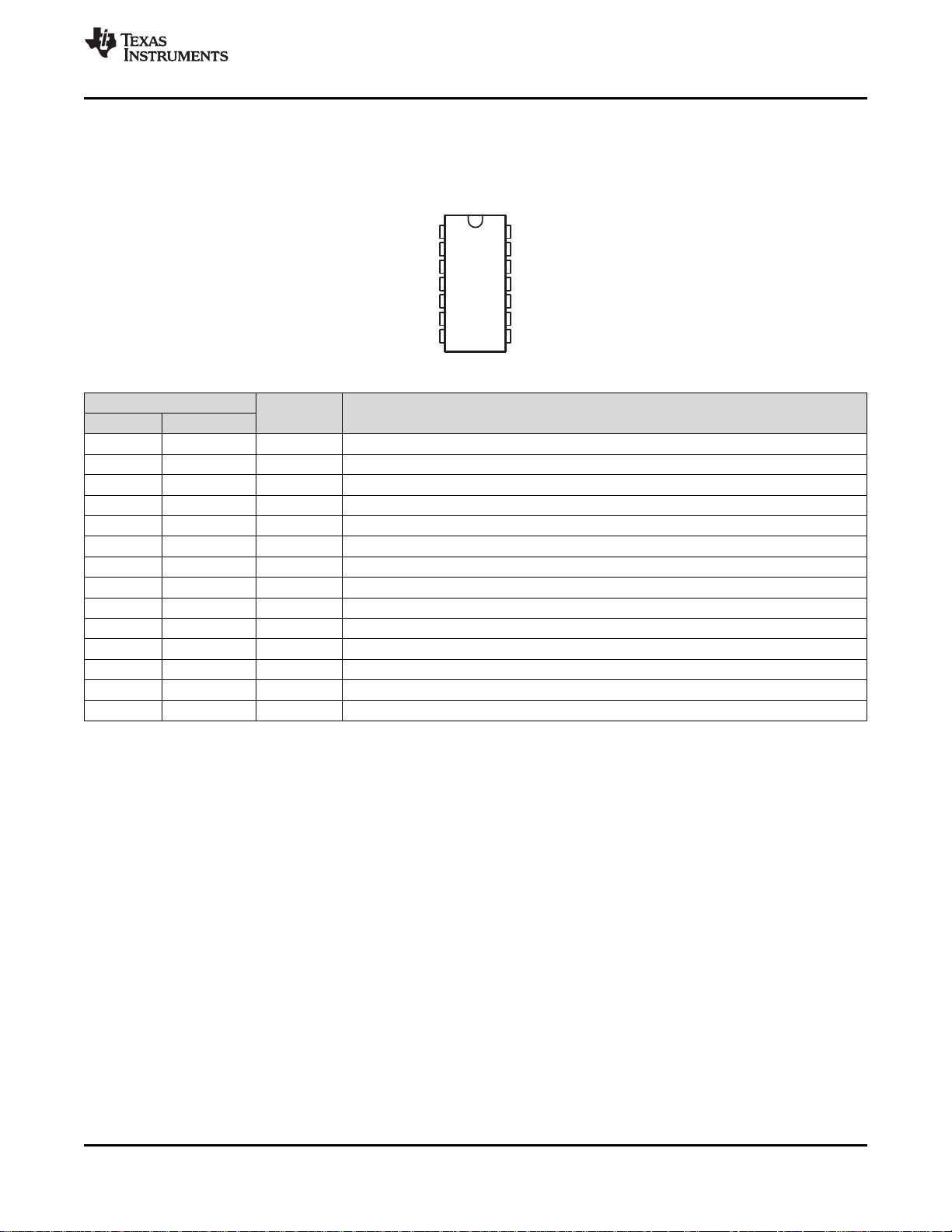
5 Pin Configuration and Functions
N, J, D, NS, or PW Packages
14-Pin PDIP, CDIP, SOIC, SO, or TSSOP
PIN
NO. NAME
I/O DESCRIPTION
1 SIG A IN/OUT I/O Input/Output for Switch A
2 SIG A OUT/IN I/O Output/Input for Switch A
3 SIG B OUT/IN I/O Output/Input for Switch B
4 SIG B IN/OUT I/O Input/Output for Switch B
5 CONTROL B I Control pin for Switch B
6 CONTROL C I Control pin for Switch C
7 V
SS
— Low Voltage Power Pin
8 SIG C IN/OUT I/O Input/Output for Switch C
9 SIG C OUT/IN I/O Output/Input for Switch C
10 SIG D OUT/IN I/O Output/Input for Switch D
11 SIG D IN/OUT I/O Input/Output for Switch D
12 CONTROL D I Control Pin for D
13 CONTROL A I Control Pin for A
14 V
DD
— Power Pin
Top View
Pin Functions
CD4066B
SCHS051H –NOVEMBER 1998–REVISED FEBRUARY 2020
Product Folder Links: CD4066B
Submit Documentation FeedbackCopyright © 1998–2020, Texas Instruments Incorporated
3
Page 4
CD4066B
SCHS051H –NOVEMBER 1998–REVISED FEBRUARY 2020
www.ti.com
6 Specifications
6.1 Absolute Maximum Ratings
Over operating free-air temperature range (unless otherwise noted)
V
DD
V
is
I
IN
T
JMAX1
T
JMAX2
T
stg
(1) Stresses beyond those listed under Absolute Maximum Ratings may cause permanent damage to the device. These are stress ratings
only, and functional operation of the device at these or any other conditions beyond those indicated under Recommended Operating
Conditions is not implied. Exposure to absolute-maximum-rated conditions for extended periods may affect device reliability.
DC supply-voltage Voltages referenced to VSSpin –0.5 20 V
Input voltage All inputs –0.5 VDD+ 0.5 V
DC input current Any one input ±10 mA
Maximum junction temperature, ceramic package 175 °C
Maximum junction temperature, plastic package 150 °C
Storage temperature –65 150 °C
6.2 ESD Ratings
Human body model (HBM), per ANSI/ESDA/JEDEC JS-001, all
(1)
V
(ESD)
Electrostatic discharge
(1) JEDEC document JEP155 states that 500-V HBM allows safe manufacturing with a standard ESD control process.
(2) JEDEC document JEP157 states that 250-V CDM allows safe manufacturing with a standard ESD control process.
pins
Charged device model (CDM), per JEDEC specification JESD22-
C101, all pins
(2)
(1)
MIN MAX UNIT
VALUE UNIT
±500
V
±1500
6.3 Recommended Operating Conditions
Over operating free-air temperature range (unless otherwise noted)
MIN MAX UNIT
V
DD
T
A
Supply voltage 3 18 V
Operating free-air temperature –55 125 °C
6.4 Thermal Information
CD4066B
THERMAL METRIC
(1)
N
(PDIP)
14 PINS 14 PINS 14 PINS 14 PINS
R
θJA
R
θJC(top)
R
θJB
ψ
JT
ψ
JB
Junction-to-ambient thermal resistance 53.7 89.5 88.2 119.5 °C/W
Junction-to-case (top) thermal resistance 41.0 49.7 46.1 48.2 °C/W
Junction-to-board thermal resistance 33.6 43.8 47.0 61.2 °C/W
Junction-to-top characterization parameter 25.8 17.4 16.3 5.5 °C/W
Junction-to-board characterization parameter 33.5 43.5 46.6 60.6 °C/W
(1) For more information about traditional and new thermal metrics, see the Semiconductor and IC Package Thermal Metrics application
report.
D
(SOIC)
NS
(SO)
PW
(TSSOP)
UNIT
4
Submit Documentation Feedback Copyright © 1998–2020, Texas Instruments Incorporated
Product Folder Links: CD4066B
Page 5
www.ti.com
6.5 Electrical Characteristics
Over operating free-air temperature range (unless otherwise noted)
PARAMETER TEST CONDITIONS MIN TYP MAX UNIT
VDD= 5 V
Vis= 0 V
VDD= 5 V
Vis= 5 V
VDD= 10 V
V
os
Switch output voltage
On-state resistance
Δr
on
difference between any
two switches
THD Total harmonic distortion
–3-dB cutoff frequency
(switch on)
–50-dB feedthrough
frequency (switch off)
–50-dB crosstalk
frequency
C
is
C
os
C
ios
V
IHC
Input capacitance VDD= 5 V, VC= VSS= –5 V 8 pF
Output capacitance VDD= 5 V, VC= VSS= –5 V 8 pF
Feedthrough VDD= 5 V, VC= VSS= –5 V 0.5 pF
Control input, high voltage See Figure 7
Crosstalk
(control input to signal
output)
Turnon and turnoff
propagation delay
Maximum control input
repetition rate
C
I
Input capacitance 5 7.5 pF
Vis= 0 V
VDD= 10 V
Vis= 10 V
VDD= 15 V
Vis= 0 V
VDD= 15 V
Vis= 15 V
VDD= 5 V 15
RL= 10 kΩ, VC= V
DD
VDD= 15 V 5
VC= VDD= 5 V, VSS= –5 V,
V
= 5 V (sine wave centered on 0 V),
is(p-p)
RL= 10 kΩ, fis= 1-kHz sine wave
VC= VDD= 5 V, VSS= –5 V, V
(sine wave centered on 0 V), RL= 1 kΩ
VC= VSS= –5 V, V
(sine wave centered on 0 V), RL= 1 kΩ
is(p-p)
is(p-p)
= 5 V
VC(A) = VDD= 5 V,
VC(B) = VSS= –5 V,
Vis(A) = 5 V
RL= 1 kΩ
, 50-Ω source,
p-p
VDD= 5 V 3.5
VDD= 15 V 11
VC= 10 V (square wave),
tr, tf= 20 ns, RL= 10 kΩ
VDD= 10 V
VDD= 5 V 35 70
VIN= VDD, tr, tf= 20 ns,
CL= 50 pF, RL= 1 kΩ
VDD= 15 V 15 30
Vis= VDD, VSS= GND,
RL= 1 kΩ to GND,
CL= 50 pF,
VDD= 5 V 6
VDD= 10 V 9
VC= 10 V (square wave
centered on 5 V), tr, tf= 20 ns,
VDD= 15 V 9.5
Vos= 1/2 Vosat 1 kHz
= 5 V
CD4066B
SCHS051H –NOVEMBER 1998–REVISED FEBRUARY 2020
0.4 V
4.6 V
0.5 V
9.5 V
1.5 V
13.5 V
ΩVDD= 10 V 10
0.4%
40 MHz
1 MHz
8 MHz
VVDD= 10 V 7
50 mV
nsVDD= 10 V 20 40
MHz
Product Folder Links: CD4066B
Submit Documentation FeedbackCopyright © 1998–2020, Texas Instruments Incorporated
5
Page 6
CD4066B
SCHS051H –NOVEMBER 1998–REVISED FEBRUARY 2020
Electrical Characteristics (continued)
Over operating free-air temperature range (unless otherwise noted)
PARAMETER TEST CONDITIONS MIN TYP MAX UNIT
TA= –55°C 0.64
VDD= 5 V
Vis= 0 V
VDD= 5 V
Vis= 5 V
VDD= 10 V
Vis= 0 V
I
is
Switch input current
VDD= 10 V
Vis= 10 V
VDD= 15 V
Vis= 0 V
VDD= 15 V
Vis= 15 V
TA= –40°C 0.61
TA= 25°C 0.51
TA= 85°C 0.42
TA= 125°C 0.36
TA= –55°C
TA= –40°C
TA= 25°C –0.51
TA= 85°C
TA= 125°C
TA= –55°C 1.6
TA= –40°C 1.5
TA= 25°C 1.3
TA= 85°C 1.1
TA= 125°C 0.9
TA= –55°C –1.6
TA= –40°C –1.5
TA= 25°C –1.3
TA= 85°C –1.1
TA= 125°C –0.9
TA= –55°C 4.2
TA= –40°C 4
TA= 25°C 3.4
TA= 85°C 2.8
TA= 125°C 2.4
TA= –55°C –4.2
TA= –40°C –4
TA= 25°C –3.4
TA= 85°C –2.8
TA= 125°C –2.4
www.ti.com
mA
–0.6
4
–0.6
1
mA
–0.4
2
–0.3
6
mA
mA
mA
mA
6
Submit Documentation Feedback Copyright © 1998–2020, Texas Instruments Incorporated
Product Folder Links: CD4066B
Page 7
V
DD
V
SS
-
(
)
www.ti.com
Electrical Characteristics (continued)
Over operating free-air temperature range (unless otherwise noted)
PARAMETER TEST CONDITIONS MIN TYP MAX UNIT
TA= –55°C 0.25
VIN= 0 to 5 V
VDD= 5 V
VIN= 0 to 10 V
VDD= 10 V
I
DD
Quiescent device current
VIN= 0 to 15 V
VDD= 15 V
VIN= 0 to 20 V
VDD= 20 V
r
on
On-state resistance (max)
to
VC= V
DD,
RL= 10 kΩ returned Vis= V
to V
DD
TA= –40°C 0.25
TA= 25°C 0.01 0.25
TA= 85°C 7.5
TA= 125°C 7.5
TA= –55°C 0.5
TA= –40°C 0.5
TA= 25°C 0.01 0.5
TA= 85°C 15
TA= 125°C 15
TA= –55°C 1
TA= –40°C 1
TA= 25°C 0.01 1
TA= 85°C 30
TA= 125°C 30
TA= –55°C 5
TA= –40°C 5
TA= 25°C 0.02 5
TA= 85°C 150
TA= 125°C 150
VDD= 5 V
VDD= 10 V
SS
VDD= 15 V
CD4066B
SCHS051H –NOVEMBER 1998–REVISED FEBRUARY 2020
µA
µA
µA
µA
TA= –55°C 800
TA= –40°C 850
TA= 25°C 470 1050
TA= 85°C 1200
TA= 125°C 1300
TA= –55°C 310
TA= –40°C 330
TA= 25°C 180 400
TA= 85°C 500
TA= 125°C 500
TA= –55°C 200
TA= –40°C 210
TA= 25°C 125 240
TA= 85°C 300
TA= 125°C 320
Ω
Submit Documentation FeedbackCopyright © 1998–2020, Texas Instruments Incorporated
7
Product Folder Links: CD4066B
Page 8
CD4066B
SCHS051H –NOVEMBER 1998–REVISED FEBRUARY 2020
Electrical Characteristics (continued)
Over operating free-air temperature range (unless otherwise noted)
PARAMETER TEST CONDITIONS MIN TYP MAX UNIT
VDD= 5 V
V
ILC
I
IN
Control input,
low voltage (max)
Input current (max)
|Iis| < 10 µA,
Vis= VSS, VOS= VDD, and
Vis= VDD, VOS= V
SS
Vis≤ VDD, VDD– VSS= 18 V,
VCC≤ VDD– V
VDD= 18 V
SS
VDD= 10 V
VDD= 15 V
TA= –55°C ±0.1
TA= –40°C ±0.1
TA= 25°C ±10–5±0.1
TA= 85°C ±1
TA= 125°C ±1
TA= –55°C 1
TA= –40°C 1
TA= 25°C 1
TA= 85°C 1
TA= 125°C 1
TA= –55°C 2
TA= –40°C 2
TA= 25°C 2
TA= 85°C 2
TA= 125°C 2
TA= –55°C 2
TA= –40°C 2
TA= 25°C 2
TA= 85°C 2
TA= 125°C 2
www.ti.com
V
µA
6.6 Switching Characteristics
TA= 25°C
PARAMETER FROM TO TEST CONDITIONS V
t
pd
t
plh
t
phl
Signal input Signal output
Signal input Signal output
Signal input Signal output
VIN= VDD, tr, tf= 20 ns,
CL= 50 pF, RL= 1 kΩ
VIN= VDD, tr, tf= 20 ns,
CL= 50 pF, RL= 1 kΩ
VIN= VDD, tr, tf= 20 ns,
CL= 50 pF, RL= 1 kΩ
CC
MIN TYP MAX UNIT
5 V 20 40
15 V 7 15
5 V 35 70
15 V 15 30
5 V 35 70
15 V 15 30
ns10 V 10 20
ns10 V 20 40
ns10 V 20 40
8
Submit Documentation Feedback Copyright © 1998–2020, Texas Instruments Incorporated
Product Folder Links: CD4066B
Page 9
3
2
1
0
−1
−2
−3
−3 −2 −1 0 1 2 3 4
VI− Input Voltage − V
92CS-30919
Output Voltage − V
V −
V
DD
VC= V
DD
V
is
V
os
R
L
V
SS
All unused terminals are
connected to V
SS
CD4066B
1 of 4
Switches
O
10
10
2
10
3
10
10
2
10
3
10
4
f − Switching Frequency − kHz
Power Dissipation Per Package − W
D
µ
6
4
2
6
4
2
6
4
2
2 4
2 4 6
P −
TA= 25°C
5 V
10 V
Supply Voltage
(VDD) = 15 V
6
V
SS
V
DD
5
6
13
12
7
CD4066B
14
8
8
Vis− Input Signal Voltage − V
300
250
200
150
100
50
0
−10 −7.5 −5 −2.5 0 2.5 5 7.5 10
Supply Voltage (VDD− VSS) = 15 V
TA= 125°C
+25 C°
−55 C°
92CS-27329RI
− Channel On-State Resistance −
on
Ω
r
Vis− Input Signal Voltage − V
600
500
400
300
200
100
0
−10 −7.5 −5 −2.5 0 2.5 5 7.5 10
Supply Voltage (VDD− VSS) = 5 V
TA= 125°C
10 V
−15 V
92CS-27330RI
− Channel On-State Resistance −
on
Ω
r
300
250
200
150
100
50
0
−10 −7.5 −5 −2.5 0 2.5 5 7.5 10
Supply Voltage (VDD− VSS) = 10 V
TA= 125°C
Vis− Input Signal Voltage − V
+25 C°
−55 C°
92CS-27327RI
− Channel On-State Resistance −
on
Ω
r
Vis− Input Signal Voltage − V
600
500
400
300
200
100
0
−4 −3 −2 −1 0 1 2 3 4
92CS-27326RI
TA= 125°C
+25 C°
−55 C°
Supply Voltage (VDD− VSS) = 5 V
− Channel On-State Resistance −
on
Ω
r
www.ti.com
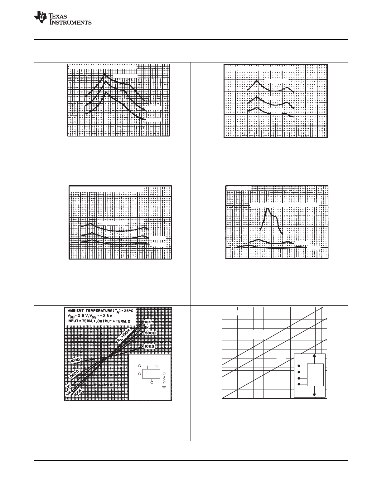
6.7 Typical Characteristics
CD4066B
SCHS051H –NOVEMBER 1998–REVISED FEBRUARY 2020
Figure 1. Typical ON-State Resistance vs Input Signal
Voltage (All Types)
Figure 3. Typical ON-State Resistance vs Input Signal
Voltage (All Types)
Figure 2. Typical ON-State Resistance vs Input Signal
Voltage (All Types)
Figure 4. Typical ON-State Resistance vs Input Signal
Voltage (All Types)
Figure 5. Typical ON Characteristics for 1 of 4 Channels
Figure 6. Power Dissipation per Package vs Switching
Frequency
Submit Documentation FeedbackCopyright © 1998–2020, Texas Instruments Incorporated
9
Product Folder Links: CD4066B
Page 10
VDD= 5 V
VC= −5 V
V
SS = −5 V
C
ios
C
is
C
os
CD4066B
1 of 4
Switches
Measured on Boonton capacitance bridge, model 75a (1 MHz);
test-fixture capacitance nulled out.
92CS-30921
X-Y
Plotter
1-kΩ
Range
TG
On
Keithley
160 Digital
Multimeter
H. P.
Moseley
7030A
X
V
SS
V
DD
10 kΩ
92CS-22716
Y
Copyright © 2016, Texas Instruments Incorporated
CD4066B
1 of 4 Switches
I
is
V
is
V
os
|Vis íVos|
|Iis|
ron =
CD4066B
SCHS051H –NOVEMBER 1998–REVISED FEBRUARY 2020
7 Parameter Measurement Information
www.ti.com
Figure 7. Determination of ronas a Test Condition for Control-Input High-Voltage (V
Figure 8. Channel On-State Resistance Measurement Circuit
) Specification
IHC
Figure 9. Typical On Characteristics for One of Four Channels
10
Submit Documentation Feedback Copyright © 1998–2020, Texas Instruments Incorporated
Product Folder Links: CD4066B
Page 11

V
DD
V
V
C
os
V
SS
CD4066B
1 of 4
Switches
V
is
+10 V
t
r
= tf= 20 ns
92CS-30924
10 kΩ
1 kΩ
All unused terminals are connected to V
SS
.
V
DD
VC= V
DD
V
os
V
SS
CD4066B
1 of 4
Switches
V
is
92CS-30923
200 kΩ
50 pF
V
DD
tr= tf= 20 ns
All unused terminals are connected to VSS.
V
DD
VC= V
SS
V
os
V
SS
CD4066B
1 of 4
Switches
Vis= V
DD
I
92CS-30922
All unused terminals are connected to VSS.
www.ti.com
CD4066B
SCHS051H –NOVEMBER 1998–REVISED FEBRUARY 2020
Parameter Measurement Information (continued)
Figure 10. Off-Switch Input or Output Leakage
Figure 11. Propagation Delay Time Signal Input
Figure 12. Crosstalk-Control Input to Signal Output
(Vis) to Signal Output (Vos)
Product Folder Links: CD4066B
Submit Documentation FeedbackCopyright © 1998–2020, Texas Instruments Incorporated
11
Page 12

V
DD
= 10 V
V
C
V
SS
CD4066B
1 of 4
Switches
V
is
= 10 V
1 kŸ50 pF
tr = tf = 20 ns
V
C
V
os
90%
10%
V
OS
VOSat1kHz
2
V
OS
VOSat1kHz
2
Repetition
Rate
50%
t
r
t
f
10 V
0 V
Copyright © 2016, Texas Instruments Incorporated
V
DD
VC=V
DD
V
os
V
SS
CD4066B
1 of 4
Switches
V
DD
1 kŸ
50 pF
V
DD
tr = tf = 20 ns
Copyright © 2016, Texas Instruments Incorporated
CD4066B
SCHS051H –NOVEMBER 1998–REVISED FEBRUARY 2020
Parameter Measurement Information (continued)
All unused pins are connected to VSS.
Delay is measured at Voslevel of +10% from ground (turn-on) or on-state output level (turn-off).
Figure 13. Propagation Delay, t
PLH
, t
Control-Signal Output
PHL
www.ti.com
All unused pins are connected to VSS.
Figure 14. Maximum Allowable Control-Input Repetition Rate
12
Submit Documentation Feedback Copyright © 1998–2020, Texas Instruments Incorporated
Product Folder Links: CD4066B
Page 13

Channel 1
Channel 2
Channel 3
Channel 4
Channel 1
Channel 2
Channel 3
Channel 4
1/4 CD4066B
CD4066B
CD4066B
CD4018B
CD4018B
1/4 CD4066B
CD4001B
LPF
LPF
LPF
LPF
1
10
5
14
15
13
1
2
3
5
2
4
1
2
5
6
8
9
12
13
3
4
10
1
8
4
11
11
12
6
9
10
2
3
10
14
15
1
5
7
9
6
10
13
11 10
3
12
11
5
8
4
3
11
4
1
2
3
9
10
PEJ1J2J3J4J
5
Q
2Q1
1/3 CD4049B
CD4001B
Signal
Inputs
Clock
Reset
1/3 CD4049B
1/6 CD4049B
10 NŸ
Signal
Outputs
P
E
J1J
2
J
3
J4J
5
Q
2
Q
1
External
Reset
Clock
10 kŸ
2 3
7 9
12
4
12 9
8 6
5
2
1
2 3 7 9 12
4
5
13
12
6
5
11
10 NŸ
10 NŸ
10 NŸ
4
Copyright © 2016, Texas Instruments Incorporated
Inputs
V
SS
Measure inputs sequentially to both VDDand VSS. Connect all unused inputs to either VDDor VSS. Measure control inputs only.
I
V
SS
V
DD
92CS-27555
V
DD
www.ti.com
CD4066B
SCHS051H –NOVEMBER 1998–REVISED FEBRUARY 2020
Parameter Measurement Information (continued)
Figure 15. Input Leakage-Current Test Circuit
Figure 16. Four-Channel PAM Multiplex System Diagram
Submit Documentation FeedbackCopyright © 1998–2020, Texas Instruments Incorporated
Product Folder Links: CD4066B
13
Page 14

Control
V
C
(1)
V
DD
V
SS
V
SS
n
n
p
Out
V
os
Control
Switch
In
n
p
V
is
CMOS Protection Network
Copyright © 2016, Texas Instruments Incorporated
CD4066B
SCHS051H –NOVEMBER 1998–REVISED FEBRUARY 2020
www.ti.com
8 Detailed Description
8.1 Overview
CD4066B has four independent digitally controlled analog switches with a bias voltage of VSSto allow for
different voltage levels to be used for low output. Both the p and the n devices in a given switch are biased on or
off simultaneously by the control signal. As shown in Figure 17, the well of the n-channel device on each switch
is tied to either the input (when the switch is on) or to VSS(when the switch is off). Thus, when the control of the
device is low, the output of the switch goes to VSSand when the control is high the output of the device goes to
VDD.
8.2 Functional Block Diagram
(1) All control inputs are protected by the CMOS protection network.
(2) All p substrates are connected to VDD.
(3) Normal operation control-line biasing: switch on (logic 1), VC= VDD; switch off (logic 0), VC= VSS.
(4) Signal-level range: VSS≤ Vis≤ VDD.
Figure 17. Schematic Diagram of One-of-Four Identical Switches and Associated Control Circuitry
8.3 Feature Description
Each switch has different control pins, which allows for more options for the outputs. Bias Voltage allows the
device to output a voltage other than 0 V when the device control is low. The CD4066B has a large absolute
maximum voltage for VDDof 20 V.
8.4 Device Functional Modes
Added Junction Temperature details to the Absolute Maximum Ratings table lists the functions of this device.
Table 1. Function Table
INPUTS OUTPUT
SIG IN/OUT CONTROL SIG OUT/IN
H H H
L H L
X L Hi-Z
14
Submit Documentation Feedback Copyright © 1998–2020, Texas Instruments Incorporated
Product Folder Links: CD4066B
Page 15

SW
SW
SW
SW
A
B
C
D
92CS-30927
Analog Inputs (±5 V)
V
DD
= 5 V
VDD= 5 V
5 V
−5 V
5 V
CD4066B
Analog Outputs (±5 V)
V
SS
= −5 V
CD4054B
V
SS
= 0 V
V
EE
= −5 V
IN
0
Digital
Control
Inputs
0
CD4066B
www.ti.com
SCHS051H –NOVEMBER 1998–REVISED FEBRUARY 2020
9 Application and Implementation
NOTE
Information in the following applications sections is not part of the TI component
specification, and TI does not warrant its accuracy or completeness. TI’s customers are
responsible for determining suitability of components for their purposes. Customers should
validate and test their design implementation to confirm system functionality.
9.1 Application Information
In applications that employ separate power sources to drive VDDand the signal inputs, the VDDcurrent capability
should exceed VDD/RL(RL= effective external load of the four CD4066B device bilateral switches). This provision
avoids any permanent current flow or clamp action on the VDDsupply when power is applied or removed from the
CD4066B device.
In certain applications, the external load-resistor current can include both VDDand signal-line components. To
avoid drawing VDDcurrent when switch current flows into pins 1, 4, 8, or 11, the voltage drop across the
bidirectional switch must not exceed 0.8 V (calculated from ronvalues shown).
No VDDcurrent flows through RLif the switch current flows into pins 2, 3, 9, or 10.
9.2 Typical Application
Figure 18. Bidirectional Signal Transmission Through Digital Control Logic
9.2.1 Design Requirements
This device uses CMOS technology and has balanced output drive. Avoid bus contention because it can drive
currents in excess of maximum limits. The high drive also creates fast edges into light loads, so consider routing
and load conditions to prevent ringing.
9.2.2 Detailed Design Procedure
1. Recommended Input Conditions:
– For rise time and fall time specifications, see Δt/Δv in Recommended Operating Conditions.
– For specified high and low levels, see VIHand VILin Recommended Operating Conditions.
2. Recommended Output Conditions:
– Load currents should not exceed ±10 mA.
Submit Documentation FeedbackCopyright © 1998–2020, Texas Instruments Incorporated
Product Folder Links: CD4066B
15
Page 16

10
10
2
10
3
10
10
2
10
3
10
4
f − Switching Frequency − kHz
Power Dissipation Per Package − W
D
µ
6
4
2
6
4
2
6
4
2
2 4
2 4 6
P −
TA= 25°C
5 V
10 V
Supply Voltage
(VDD) = 15 V
6
V
SS
V
DD
5
6
13
12
7
CD4066B
14
8
8
CD4066B
SCHS051H –NOVEMBER 1998–REVISED FEBRUARY 2020
Typical Application (continued)
9.2.3 Application Curve
Figure 19. Power Dissipation vs. Switching Frequency
www.ti.com
16
Submit Documentation Feedback Copyright © 1998–2020, Texas Instruments Incorporated
Product Folder Links: CD4066B
Page 17

V
cc
Unused Input
Input
Output
Input
Unused Input
Output
CD4066B
www.ti.com
SCHS051H –NOVEMBER 1998–REVISED FEBRUARY 2020
10 Power Supply Recommendations
The power supply can be any voltage between the MIN and MAX supply voltage rating located in Recommended
Operating Conditions.
Each VCC pin should have a good bypass capacitor to prevent power disturbance. For devices with a single
supply, 0.1-µF is recommended; if there are multiple VCC pins, then 0.01-µF or 0.022-µF is recommended for
each power pin. It is acceptable to parallel multiple bypass capacitors to reject different frequencies of noise. A
0.1-µF and a 1-µF are commonly used in parallel. The bypass capacitor should be installed as close to the power
pin as possible for best results.
11 Layout
11.1 Layout Guidelines
When using multiple bit logic devices inputs must never float.
In many cases, functions or parts of functions of digital logic devices are unused, for example, when only two
inputs of a triple-input and gate are used or only 3 of the 4 buffer gates are used. Such input pins must not be left
unconnected because the undefined voltages at the outside connections result in undefined operational states.
All unused inputs of digital logic devices must be connected to a high or low bias to prevent them from floating.
The logic level that should be applied to any particular unused input depends on the function of the device.
Generally they are tied to GND or VCC, whichever makes more sense or is more convenient. It is generally
acceptable to float outputs, unless the part is a transceiver. If the transceiver has an output enable pin, it disables
the output section of the part when asserted. This does not disable the input section of the I/Os, so they cannot
float when disabled.
11.2 Layout Example
Figure 20. Diagram for Unused Inputs
Product Folder Links: CD4066B
Submit Documentation FeedbackCopyright © 1998–2020, Texas Instruments Incorporated
17
Page 18

CD4066B
SCHS051H –NOVEMBER 1998–REVISED FEBRUARY 2020
www.ti.com
12 Device and Documentation Support
12.1 Receiving Notification of Documentation Updates
To receive notification of documentation updates, navigate to the device product folder on ti.com. In the upper
right corner, click on Alert me to register and receive a weekly digest of any product information that has
changed. For change details, review the revision history included in any revised document.
12.2 Community Resources
TI E2E™ support forums are an engineer's go-to source for fast, verified answers and design help — straight
from the experts. Search existing answers or ask your own question to get the quick design help you need.
Linked content is provided "AS IS" by the respective contributors. They do not constitute TI specifications and do
not necessarily reflect TI's views; see TI's Terms of Use.
12.3 Trademarks
E2E is a trademark of Texas Instruments.
All other trademarks are the property of their respective owners.
12.4 Electrostatic Discharge Caution
This integrated circuit can be damaged by ESD. Texas Instruments recommends that all integrated circuits be handled with
appropriate precautions. Failure to observe proper handling and installation procedures can cause damage.
ESD damage can range from subtle performance degradation to complete device failure. Precision integrated circuits may be more
susceptible to damage because very small parametric changes could cause the device not to meet its published specifications.
12.5 Glossary
SLYZ022 — TI Glossary.
This glossary lists and explains terms, acronyms, and definitions.
13 Mechanical, Packaging, and Orderable Information
The following pages include mechanical, packaging, and orderable information. This information is the most
current data available for the designated devices. This data is subject to change without notice and revision of
this document. For browser-based versions of this data sheet, refer to the left-hand navigation.
18
Submit Documentation Feedback Copyright © 1998–2020, Texas Instruments Incorporated
Product Folder Links: CD4066B
Page 19

PACKAGE OPTION ADDENDUM
www.ti.com
PACKAGING INFORMATION
Orderable Device Status
CD4066BE ACTIVE PDIP N 14 25 Green (RoHS
CD4066BEE4 ACTIVE PDIP N 14 25 Pb-Free
CD4066BF ACTIVE CDIP J 14 1 TBD Call TI N / A for Pkg Type -55 to 125 CD4066BF
CD4066BF3A ACTIVE CDIP J 14 1 TBD Call TI N / A for Pkg Type -55 to 125 CD4066BF3A
CD4066BM ACTIVE SOIC D 14 50 Green (RoHS
CD4066BM96 ACTIVE SOIC D 14 2500 Green (RoHS
CD4066BM96E4 ACTIVE SOIC D 14 2500 Green (RoHS
CD4066BM96G4 ACTIVE SOIC D 14 2500 Green (RoHS
CD4066BMT ACTIVE SOIC D 14 250 Green (RoHS
CD4066BNS ACTIVE SO NS 14 50 Green (RoHS
CD4066BNSR ACTIVE SO NS 14 2000 Green (RoHS
CD4066BPW ACTIVE TSSOP PW 14 90 Green (RoHS
CD4066BPWG4 ACTIVE TSSOP PW 14 90 Green (RoHS
CD4066BPWR ACTIVE TSSOP PW 14 2000 Green (RoHS
CD4066BPWRG4 ACTIVE TSSOP PW 14 2000 Green (RoHS
JM38510/05852BCA ACTIVE CDIP J 14 1 TBD Call TI N / A for Pkg Type -55 to 125 JM38510/
M38510/05852BCA ACTIVE CDIP J 14 1 TBD Call TI N / A for Pkg Type -55 to 125 JM38510/
Package Type Package
(1)
Drawing
Pins Package
Qty
Eco Plan
(2)
& no Sb/Br)
(RoHS)
& no Sb/Br)
& no Sb/Br)
& no Sb/Br)
& no Sb/Br)
& no Sb/Br)
& no Sb/Br)
& no Sb/Br)
& no Sb/Br)
& no Sb/Br)
& no Sb/Br)
& no Sb/Br)
Lead/Ball Finish
(6)
MSL Peak Temp
(3)
Op Temp (°C) Device Marking
NIPDAU | SN N / A for Pkg Type -55 to 125 CD4066BE
NIPDAU N / A for Pkg Type -55 to 125 CD4066BE
NIPDAU Level-1-260C-UNLIM -55 to 125 CD4066BM
NIPDAU | SN Level-1-260C-UNLIM -55 to 125 CD4066BM
NIPDAU Level-1-260C-UNLIM -55 to 125 CD4066BM
NIPDAU Level-1-260C-UNLIM -55 to 125 CD4066BM
NIPDAU Level-1-260C-UNLIM -55 to 125 CD4066BM
NIPDAU Level-1-260C-UNLIM CD4066B
NIPDAU Level-1-260C-UNLIM -55 to 125 CD4066B
NIPDAU Level-1-260C-UNLIM -55 to 125 CM066B
NIPDAU Level-1-260C-UNLIM -55 to 125 CM066B
NIPDAU | SN Level-1-260C-UNLIM -55 to 125 CM066B
NIPDAU Level-1-260C-UNLIM -55 to 125 CM066B
6-Feb-2020
Samples
(4/5)
05852BCA
05852BCA
Addendum-Page 1
Page 20

PACKAGE OPTION ADDENDUM
www.ti.com
(1)
The marketing status values are defined as follows:
ACTIVE: Product device recommended for new designs.
LIFEBUY: TI has announced that the device will be discontinued, and a lifetime-buy period is in effect.
NRND: Not recommended for new designs. Device is in production to support existing customers, but TI does not recommend using this part in a new design.
PREVIEW: Device has been announced but is not in production. Samples may or may not be available.
OBSOLETE: TI has discontinued the production of the device.
(2)
RoHS: TI defines "RoHS" to mean semiconductor products that are compliant with the current EU RoHS requirements for all 10 RoHS substances, including the requirement that RoHS substance
do not exceed 0.1% by weight in homogeneous materials. Where designed to be soldered at high temperatures, "RoHS" products are suitable for use in specified lead-free processes. TI may
reference these types of products as "Pb-Free".
RoHS Exempt: TI defines "RoHS Exempt" to mean products that contain lead but are compliant with EU RoHS pursuant to a specific EU RoHS exemption.
Green: TI defines "Green" to mean the content of Chlorine (Cl) and Bromine (Br) based flame retardants meet JS709B low halogen requirements of <=1000ppm threshold. Antimony trioxide based
flame retardants must also meet the <=1000ppm threshold requirement.
(3)
MSL, Peak Temp. - The Moisture Sensitivity Level rating according to the JEDEC industry standard classifications, and peak solder temperature.
(4)
There may be additional marking, which relates to the logo, the lot trace code information, or the environmental category on the device.
(5)
Multiple Device Markings will be inside parentheses. Only one Device Marking contained in parentheses and separated by a "~" will appear on a device. If a line is indented then it is a continuation
of the previous line and the two combined represent the entire Device Marking for that device.
(6)
Lead/Ball Finish - Orderable Devices may have multiple material finish options. Finish options are separated by a vertical ruled line. Lead/Ball Finish values may wrap to two lines if the finish
value exceeds the maximum column width.
Important Information and Disclaimer:The information provided on this page represents TI's knowledge and belief as of the date that it is provided. TI bases its knowledge and belief on information
provided by third parties, and makes no representation or warranty as to the accuracy of such information. Efforts are underway to better integrate information from third parties. TI has taken and
continues to take reasonable steps to provide representative and accurate information but may not have conducted destructive testing or chemical analysis on incoming materials and chemicals.
TI and TI suppliers consider certain information to be proprietary, and thus CAS numbers and other limited information may not be available for release.
In no event shall TI's liability arising out of such information exceed the total purchase price of the TI part(s) at issue in this document sold by TI to Customer on an annual basis.
OTHER QUALIFIED VERSIONS OF CD4066B, CD4066B-MIL :
Catalog: CD4066B
•
6-Feb-2020
Automotive: CD4066B-Q1, CD4066B-Q1
•
Military: CD4066B-MIL
•
Addendum-Page 2
Page 21

PACKAGE OPTION ADDENDUM
www.ti.com
NOTE: Qualified Version Definitions:
Catalog - TI's standard catalog product
•
Automotive - Q100 devices qualified for high-reliability automotive applications targeting zero defects
•
Military - QML certified for Military and Defense Applications
•
6-Feb-2020
Addendum-Page 3
Page 22

PACKAGE MATERIALS INFORMATION
www.ti.com 28-Jan-2020
TAPE AND REEL INFORMATION
*All dimensions are nominal
Device Package
Type
CD4066BM96 SOIC D 14 2500 330.0 16.4 6.5 9.0 2.1 8.0 16.0 Q1
CD4066BM96 SOIC D 14 2500 330.0 16.8 6.5 9.5 2.1 8.0 16.0 Q1
CD4066BM96 SOIC D 14 2500 330.0 16.4 6.5 9.0 2.1 8.0 16.0 Q1
CD4066BM96G4 SOIC D 14 2500 330.0 16.4 6.5 9.0 2.1 8.0 16.0 Q1
CD4066BM96G4 SOIC D 14 2500 330.0 16.4 6.5 9.0 2.1 8.0 16.0 Q1
CD4066BMT SOIC D 14 250 330.0 16.4 6.5 9.0 2.1 8.0 16.0 Q1
CD4066BNSR SO NS 14 2000 330.0 16.4 8.2 10.5 2.5 12.0 16.0 Q1
CD4066BPWR TSSOP PW 14 2000 330.0 12.4 6.9 5.6 1.6 8.0 12.0 Q1
CD4066BPWR TSSOP PW 14 2000 330.0 12.4 6.9 5.6 1.6 8.0 12.0 Q1
CD4066BPWRG4 TSSOP PW 14 2000 330.0 12.4 6.9 5.6 1.6 8.0 12.0 Q1
Package
Drawing
Pins SPQ Reel
Diameter
(mm)
Reel
Width
W1 (mm)
A0
(mm)B0(mm)K0(mm)P1(mm)W(mm)
Pin1
Quadrant
Pack Materials-Page 1
Page 23

PACKAGE MATERIALS INFORMATION
www.ti.com 28-Jan-2020
*All dimensions are nominal
Device Package Type Package Drawing Pins SPQ Length (mm) Width (mm) Height (mm)
CD4066BM96 SOIC D 14 2500 333.2 345.9 28.6
CD4066BM96 SOIC D 14 2500 364.0 364.0 27.0
CD4066BM96 SOIC D 14 2500 367.0 367.0 38.0
CD4066BM96G4 SOIC D 14 2500 333.2 345.9 28.6
CD4066BM96G4 SOIC D 14 2500 367.0 367.0 38.0
CD4066BMT SOIC D 14 250 210.0 185.0 35.0
CD4066BNSR SO NS 14 2000 367.0 367.0 38.0
CD4066BPWR TSSOP PW 14 2000 367.0 367.0 35.0
CD4066BPWR TSSOP PW 14 2000 364.0 364.0 27.0
CD4066BPWRG4 TSSOP PW 14 2000 367.0 367.0 35.0
Pack Materials-Page 2
Page 24

Page 25

Page 26

PACKAGE OUTLINE
12X .100
[2.54]
PIN 1 ID
(OPTIONAL)
1
14
A
-.785.754
-19.9419.15[ ]
SCALE 0.900
4X .005 MIN
14X -.065.045
[0.13]
-1.651.15[ ]
CDIP - 5.08 mm max heightJ0014A
CERAMIC DUAL IN LINE PACKAGE
TYP-.060.015
-1.520.38[ ]
14X -.026.014
-0.660.36[ ]
.010 [0.25] C A B
7
B -.283.245
AT GAGE PLANE
NOTES:
1. All controlling linear dimensions are in inches. Dimensions in brackets are in millimeters. Any dimension in brackets or parenthesis are for
reference only. Dimensioning and tolerancing per ASME Y14.5M.
2. This drawing is subject to change without notice.
3. This package is hermitically sealed with a ceramic lid using glass frit.
4. Index point is provided on cap for terminal identification only and on press ceramic glass frit seal only.
5. Falls within MIL-STD-1835 and GDIP1-T14.
0
-7.196.22[ ]
-.314.308
-7.977.83[ ]
-15
TYP
8
.015 GAGE PLANE
[0.38]
14X .008-.014
[0.2-0.36]
.2 MAX TYP
[5.08]
C
.13 MIN TYP
[3.3]
SEATING PLANE
4214771/A 05/2017
www.ti.com
Page 27

SEE DETAIL A
(.300 ) TYP
[7.62]
EXAMPLE BOARD LAYOUT
CDIP - 5.08 mm max heightJ0014A
CERAMIC DUAL IN LINE PACKAGE
SEE DETAIL B
12X (.100 )
[2.54]
14X ( .039)
[1]
1
7
SYMM
LAND PATTERN EXAMPLE
NON-SOLDER MASK DEFINED
SCALE: 5X
14
SYMM
8
MAX.002
[0.05]
ALL AROUND
(R.002 ) TYP
[0.05]
(.063)
[1.6]
DETAIL A
SCALE: 15X
SOLDER MASK
OPENING
METAL
www.ti.com
METAL
SOLDER MASK
OPENING
( .063)
[1.6]
.002 MAX
[0.05]
ALL AROUND
DETAIL B
13X, SCALE: 15X
4214771/A 05/2017
Page 28

Page 29

Page 30

Page 31

Page 32

Page 33

IMPORTANT NOTICE AND DISCLAIMER
TI PROVIDES TECHNICAL AND RELIABILITY DATA (INCLUDING DATASHEETS), DESIGN RESOURCES (INCLUDING REFERENCE
DESIGNS), APPLICATION OR OTHER DESIGN ADVICE, WEB TOOLS, SAFETY INFORMATION, AND OTHER RESOURCES “AS IS”
AND WITH ALL FAULTS, AND DISCLAIMS ALL WARRANTIES, EXPRESS AND IMPLIED, INCLUDING WITHOUT LIMITATION ANY
IMPLIED WARRANTIES OF MERCHANTABILITY, FITNESS FOR A PARTICULAR PURPOSE OR NON-INFRINGEMENT OF THIRD
PARTY INTELLECTUAL PROPERTY RIGHTS.
These resources are intended for skilled developers designing with TI products. You are solely responsible for (1) selecting the appropriate
TI products for your application, (2) designing, validating and testing your application, and (3) ensuring your application meets applicable
standards, and any other safety, security, or other requirements. These resources are subject to change without notice. TI grants you
permission to use these resources only for development of an application that uses the TI products described in the resource. Other
reproduction and display of these resources is prohibited. No license is granted to any other TI intellectual property right or to any third
party intellectual property right. TI disclaims responsibility for, and you will fully indemnify TI and its representatives against, any claims,
damages, costs, losses, and liabilities arising out of your use of these resources.
TI’s products are provided subject to TI’s Terms of Sale (www.ti.com/legal/termsofsale.html) or other applicable terms available either on
ti.com or provided in conjunction with such TI products. TI’s provision of these resources does not expand or otherwise alter TI’s applicable
warranties or warranty disclaimers for TI products.
Mailing Address: Texas Instruments, Post Office Box 655303, Dallas, Texas 75265
Copyright © 2020, Texas Instruments Incorporated
 Loading...