

Page 1

User Guide
2014
SimpleLink is a trademark of Texas Instruments Incorporated.
TI Proprietary Information - Strictly Private
1
CC3100BOOST (CC3100 Booster Pack) User Guide, Ver 1.1
ECS Applications
ABSTRACT
This document describes the CC3100BOOST (CC3100 Booster Pack). It details the features of
the hardware and also explains the correct usage of the board.
ABSTRACT
This document describes the CC3100BOOST (CC3100 Booster Pack). It details the features
of the hardware and also explains the correct usage of the board.
Page 2

CC3100BOOST User Guide
TI Proprietary Information - Strictly Private
TABLE OF CONTENTS
1 Introduction ................................................................................................................................ 4
2 Overview ...................................................................................................................................... 4
3 Hardware description ................................................................................................................ 4
3.1 Board overview ....................................................................................................................... 4
3.2 Board features ........................................................................................................................ 5
3.3 Jumper and connector information ......................................................................................... 6
3.3.1 2x20 pin connector ...................................................................................................... 6
3.4 Jumper details ........................................................................................................................ 7
3.5 LED and switches .................................................................................................................... 8
3.6 Conducted testing ................................................................................................................... 9
3.7 Current measurement ........................................................................................................... 10
4 Connecting to a PC using FTDI Board ................................................................................... 11
4.1 Jumper settings on the BP Board .......................................................................................... 11
4.2 Jumper settings on the FTDI Board ...................................................................................... 12
4.3 FTDI Board details ................................................................................................................ 13
4.3.1 Overview ................................................................................................................... 13
4.3.2 Hardware details ....................................................................................................... 14
4.3.3 Driver requirements .................................................................................................. 15
5 Connecting to a Launchpad .................................................................................................... 16
5.1 Launchpad current limitation ................................................................................................ 16
5.2 Connecting to an experimenter’s board. ............................................................................... 18
Page 3

CC3100BOOST User Guide
TI Proprietary Information - Strictly Private
Page 4

CC3100BOOST User Guide
TI Proprietary Information - Strictly Private
1 Introduction
This document provides a quick start guide on using the CC3100 Booster Pack Rev 2.0B .
This is not applicable to other revisions of the board.
2 Overview
The CC3100 Booster Pack is a board designed to interface with the TI standard Launchpad
including the Tiva-C series and the MSP430 value line launchpads. In addition to the
launchpads, there is support available to mate the board with a FTDI Debug board to
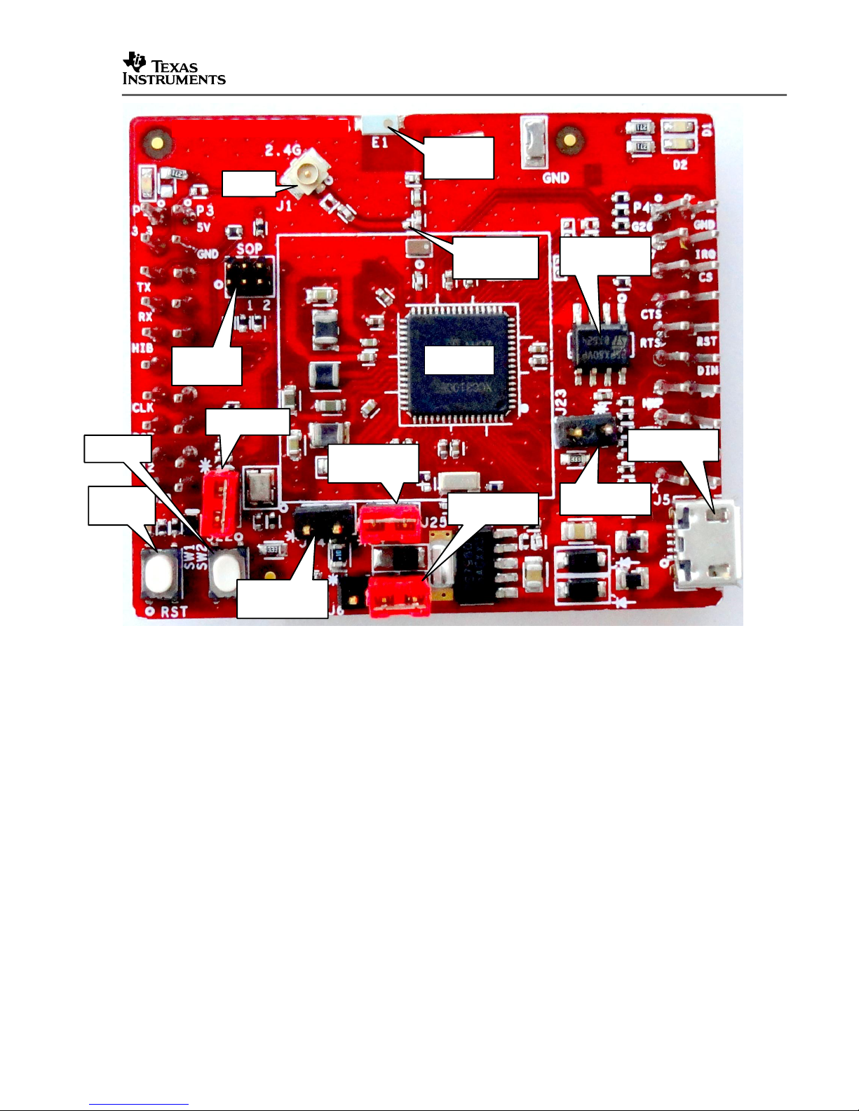
interface directly to a PC host using USB cable. A picture of the board is presented below
with the main components marked.
3 Hardware description
3.1 Board overview
Page 5
CC3100BOOST User Guide
TI Proprietary Information - Strictly Private
FIGU RE 1 : HAR DWARE DETAIL S
3.2 Board features
2x20 pin stackable connectors
On-board chip antenna with option for U.FL based conducted testing.
Power from on-board LDO using USB OR 3.3V from MCU Launchpad
Push buttons (2x)
LEDs (4x)
Jumper with 0.1 Ohm resistor for current measurement.
.8 Mbit serial flash
40 MHz crystal , 32KHz crystal and oscillator.
CC3100
RESET
Current
Measurement
RESET
BUTTON
Sense on
Power
GPIO13
U.FL
Antenna
RF SIGNAL
SELECT
TOP DIE
FLASH Vcc
CC3100 Vcc
GPIO12
USB CONN
SERIAL
FLASH
Page 6
CC3100BOOST User Guide
TI Proprietary Information - Strictly Private
4 Layer PCB with 6mil spacing and track width.
3.3 Jumper and connector information
3.3.1 2x20 pin connector
The signal assignment on the 2x20 pin connector is shown below. The convention of J1..J4
is replaced with P1…P4 to avoid confusion with the actual board reference.
Outer row connectors
Pin No
Signal Name
Direction
Pin No
Signal Name
Direction
P1.1
VCC(3.3V)
IN
P2.1
GND
IN
P1.2
UN-USED
NA
P2.2
IRQ
OUT
P1.3
UART1_TX
OUT
P2.3
SPI_CS
IN
P1.4
UART1_RX
IN
P2.4
UN-USED
NA
P1.5
nHIB
IN
P2.5
nRESET
IN
P1.6
UNUSED
NA
P2.6
SPI_MOSI
IN
P1.7
SPI_CLK
IN
P2.7
SPI_MISO
OUT
P1.8
UN-USED
NA
P2.8
UN-USED
NA
P1.9
UN-USED
NA
P2.9
UN-USED
NA
P1.10
UN-USED
NA
P2.10
UN-USED
NA
Inner row connectors
Pin No
Signal Name
Direction
Pin No
Signal Name
Direction
P3.1
+5V
IN
P4.1
ANT_SEL_1
OUT
P3.2
GND
IN
P4.2
ANT_SEL_2
OUT
P3.3
UN-USED
NA
P4.3
UN-USED
NA
P3.4
UN-USED
NA
P4.4
UART1_CTS
IN
P3.5
UN-USED
NA
P4.5
UART1_RTS
OUT
P3.6
UN-USED
NA
P4.6
UN-USED
NA
P3.7
UN-USED
NA
P4.7
NWP_LOG_TX
OUT
P3.8
UN-USED
NA
P4.8
WLAN_LOG_TX
OUT
P3.9
UN-USED
NA
P4.9
WL_RS232_RX
IN
P3.10
UN-USED
NA
P4.10
WL_RS232_TX
OUT
Note : All signals are 3.3V COMS logic levels and is referred w.r.t. CC3100 IC. For e.g.
UART1_TX is an output from the CC3100.
Page 7

CC3100BOOST User Guide
TI Proprietary Information - Strictly Private
For the SPI lines, the CC3100 always acts like a slave.
3.4 Jumper details
Reference
Usage
Comments
J5
USB connector
For powering the booster pack when
mated with a Launchpad
J6
Power selection
Choose the power supply from the
Lauchpad or the on-board USB.
J6 (1-2) power from MCU Launchpad
J6 (2-3) power from on-board USB using
3.3V LDO
J24
Current
measurement
Voltage is measured across the 0.1 Ohm
resistor using a voltmeter.
Can be used for IDLE and Active
currents.
For Hibernate currents, remove R42 and
connect a ammeter across J24. Range
(< 100uA)
J23
OOB Demo
Closed : GPIO_12 is hard pulled to Vcc
Open : GPIO_12 is pulled to GND using
33K resistor.
J22
RESET
Closed : Routes the RESET signal from
the MCU Launchpad to the CC3100.
Open : The RESET is cut off from the
MCU. (Used with MSP430 boards where
RESET line is muxed with TEST)
J8,J7
Booster pack header
2x10 pins each connected to the
Launchpad.
J25
Flash power
Power the top die flash of the CC3100Z
Page 8

CC3100BOOST User Guide
TI Proprietary Information - Strictly Private
part with 3.3V LDO.
Install this for all boards with the
CC3100Z parts.
J2
Sense on power
Sense on power used for internal debug.
SOP[2:0] = 000 [Functional 4W]
SOP[2:0] = 001 [Functional 2W]
SOP[2:0] = 010 [Load from EEPROM]
SOP[2:0] = 011 [Boot Debug mode]
SOP[2:0] = 100 [UART LOAD]
SOP[2:0] = 101 [TESTMODE 3]
SOP[2:0] = 110 [TESTMODE 2]
SOP[2:0] = 111 [TESTMODE 1]
J1
RF Test
U.FL connector for conducted testing.
3.5 LED and switches
Reference
Usage
Comments
SW1
RESET
Reset the CC3100 when mated with the
LP or FTDI board. Useful while updating
the flash contents.
SW2
OOB Demo
Pull GPIO_13 to Vcc when pressed.
D1
GPIO_09
Yellow LED to indicate state of GPIO_09.
LED glows when GPIO_09 goes low.
D2
GPIO_08
GREEN LED to indicate state of
Page 9

CC3100BOOST User Guide
TI Proprietary Information - Strictly Private
GPIO_08.
LED glows when GPIO_08 goes low.
D7
nHIB
Green LED
Glows when the CC3100 device is
enabled using nHIB.
D5
Power
RED LED to indicate the power line
status.
Note : This LED can glow if the board is
powered from any of the GPIO being
high, and the Vcc is un-connected. This
is not a valid state and should be
avoided.
3.6 Conducted testing
The board is by default configured for radiated measurement using the on-board chip
antenna. For conducted testing in the lab the following changes needs to be done on the
board.
Mode
Change
Image
Conducted test
using U.FL
C4 = 10pF
C2 = DNP
Page 10

CC3100BOOST User Guide
TI Proprietary Information - Strictly Private
Radiated test
using antenna
C4 = DNP
C2 = 10pF
Note : The 10pF capacitor used should be of RF grade with high-Q to reduce the overall
loss. Otherwise a 0 Ohm resistor can also be used for this.
3.7 Current measurement
The board provides a jumper connected to a 0.1 Ohm resistor for current measurement. The
measurement is made by using a voltmeter across the jumper and multiplying the value
obtained in mV by 10 to get the current in mA. The current measurement jumper is J24 as
shown in Figure 1.
Note : The measurement may have up to 10% error due to resistor variation and contact
resistance due to reflow soldering.
Page 11

CC3100BOOST User Guide
TI Proprietary Information - Strictly Private
4 Connecting to a PC using FTDI Board
FIGU RE 2 : P C CONNECT ION U SIN G FTD I
The image above shows the connection of the Booster Pack to the FTDI Board. The
connectors should be aligned carefully considering that it does not have a polarity protection.
The pin-1 of the connectors are marked on the board using a DOT and these should be
aligned while mating.
Note : The mating and unmating force needed for these connectors may be large and may
end up breaking the boards. To prevent this caution should be restrained while unmating
these. Also , it is not recommended to mate the connectors all the way. About 3mm contact
length is good enough for the board as shown in the figure above.
4.1 Jumper settings on the BP Board
The following table specifies the jumpers to be installed while mating with the FTDI board.
No
Jumper settings
Notes
1
J6 (1-2)
Power the BP from the FTDI. The jumper shall be placed
close to the LED.
2
J25 (shorted)
The top die flash on CC3100Z devices powered from 3.3V
directly
3
J24 (open)
No current measurement
Page 12

CC3100BOOST User Guide
TI Proprietary Information - Strictly Private
4
J23 (open)
OOB demo jumper
5
SOP jumpers
All open
6
J22 (shorted)
RESET control from FTDI and BP button
After installing these jumpers the board would resemble as below
4.2 Jumper settings on the FTDI Board
The following table specifies the jumpers to be installed while mating with the FTDI board.
No
Jumper settings
Notes
1
J22, J24, J21
shorted
2
Remaining jumpers
Open
Page 13

CC3100BOOST User Guide
TI Proprietary Information - Strictly Private
After installing the jumpers, the board would resemble below
4.3 FTDI Board details
4.3.1 Overview
The FTDI Debug Board 2.0A is designed to connect the Booster pack to a PC using USB
connection. This is used to update the firmware on the BP using the “SL_Prog” utility and
also in software development using “SL_Studio”.
Page 14

CC3100BOOST User Guide
TI Proprietary Information - Strictly Private
4.3.2 Hardware details
The board has two FTDI ICs to enumerate multiple COM and D2XX ports. The details of the
ports are given below
Ports available on J1
Port No
Port Type
Usage
Comments
1
D2XX
SPI port for SL Studio
2
D2XX
GPIO for SL Studio
Control the nRESET, nHIB,
IRQ
MAC and NWP
Logger
SPI, GPIO,
UART, RT
3
Power
Page 15

CC3100BOOST User Guide
TI Proprietary Information - Strictly Private
3
VCP
COM port for flash
programming
4 VCP
RT3
For RF debug using RT3
software
Note : On the PC only two of the four ports would be visible on the Device Manager. The
D2XX ports are not listed under the “Ports” tab.
The first COM port in the list usually is used for the flash programming.
Ports available on J2
Port No
Port Type
Usage
Comments
1
VCP
MAC logg UART Tx for
WLAN Debug
2 VCP
NWP log UART Tx for
debugging
4.3.3 Driver requirements
The FTDI Debug board requires the user to install the associated drivers on a PC. This
package is available as part of the SDK release and would be located at [InstallPath]\cc3100-sdk\tools\cc31xx_board_drivers\.
The install path is usually C:\ti\cc3100SDK
For SL_Prog
Page 16

CC3100BOOST User Guide
TI Proprietary Information - Strictly Private
5 Connecting to a Launchpad
The CC3100 Booster pack can be directly connected to a compatible Launchpad using the
standard 2x20 pin connectors. The jumper settings needed for this connection is the same as
that needed for the FTDI Debug board as described in the previous section.
Please ensure that the Pin1 of the 2x20 pins are aligned correctly before mating. The mated
setup is as per the picture below. (Note the USB cable is connected to the Booster Pack
directly to power it only. For debugging, the USB cable on the Launchpad is also required)
FIGU RE 3 : B OOSTER PACK CONNE CTED TO TI VA LAUN CHP AD
5.1 Launchpad current limitation
Some of the launchpads including the MSP430FRAM launchpads do not provide enough
current to power the CC3100 booster pack. The booster pack can consume upto 400mA
peak from the 3.3V and hence it may be needed to power is separately.
For this a USB connector is provided on the Booster Pack to provide the 3.3V separately.
The power supply jumpers shall be configured as below when the power is supplied from the
on-board USB connector.
Page 17

CC3100BOOST User Guide
TI Proprietary Information - Strictly Private
FIGU RE 4 : JUM PER S ETTIN GS WH EN US ED WI TH LAUN CHP AD
Important : Since there are two power sources in this setup it is important to follow the power-up
sequence.
Note : Always power the Booster Pack before powering the Launchpad.
Page 18

CC3100BOOST User Guide
TI Proprietary Information - Strictly Private
5.2 Connecting to an experimenter’s board.
The Boosterpack could be connected to an experimenters board like the MSP430 FRAM
experimenter’s board using an EM Adapter board.
The EM adapter board converts the EM connectors to the standard 2x20 pin connectors of
the booster pack headers.
The stacked setup is as shown below. Ensure that the connectors are oriented correctly
before powering up the board.
Page 19

CC3100BOOST User Guide
TI Proprietary Information - Strictly Private
Page 20

CC3100BOOST User Guide
TI Proprietary Information - Strictly Private
Page 21

CC3100BOOST User Guide
TI Proprietary Information - Strictly Private
Page 22

CC3100BOOST User Guide
TI Proprietary Information - Strictly Private
Page 23

CC3100BOOST User Guide
TI Proprietary Information - Strictly Private
 Loading...