


CC2530F32, CC2530F64
CC2530F128, CC2530F256
www.ti.com
SWRS081B –APRIL 2009– REVISED FEBRUARY 2011
A True System-on-Chip Solution for 2.4-GHz IEEE 802.15.4 and ZigBee Applications
Check for Samples: CC2530F32, CC2530F64, CC2530F128, CC2530F256
1
FEATURES
2345
• RF/Layout
– 2.4-GHz IEEE 802.15.4 Compliant RF
– IEEE 802.15.4 MAC Timer, General-Purpose
Timers (One 16-Bit, Two 8-Bit)
– IR Generation Circuitry
Transceiver – 32-kHz Sleep Timer With Capture
– Excellent Receiver Sensitivity and – CSMA/CA Hardware Support
Robustness to Interference
– Programmable Output Power Up to 4.5 dBm
– Very Few External Components
– Accurate Digital RSSI/LQI Support
– Battery Monitor and Temperature Sensor
– 12-Bit ADC With Eight Channels and
– Only a Single Crystal Needed for Configurable Resolution
Asynchronous Networks
– 6-mm × 6-mm QFN40 Package
– AES Security Coprocessor
– Two Powerful USARTs With Support for
– Suitable for Systems Targeting Compliance Several Serial Protocols
With Worldwide Radio-Frequency
Regulations: ETSI EN 300 328 and EN 300
440 (Europe), FCC CFR47 Part 15 (US) and
ARIB STD-T-66 (Japan)
• Low Power
– Active-Mode RX (CPU Idle): 24 mA
– Active Mode TX at 1 dBm (CPU Idle): 29 mA
– Power Mode 1 (4 μs Wake-Up): 0.2 mA
– Power Mode 2 (Sleep Timer Running): 1 μA
– Power Mode 3 (External Interrupts): 0.4 μA
– Wide Supply-Voltage Range (2 V–3.6 V)
– 21 General-Purpose I/O Pins
(19 × 4 mA, 2 × 20 mA)
– Watchdog Timer
• Development Tools
– CC2530 Development Kit
– CC2530 ZigBee®Development Kit
– CC2530 RemoTI™ Development Kit for
RF4CE
– SmartRF™ Software
– Packet Sniffer
– IAR Embedded Workbench™ Available
• Microcontroller
– High-Performance and Low-Power 8051 APPLICATIONS
Microcontroller Core With Code Prefetch
– 32-, 64-, 128-, or 256-KB
In-System-Programmable Flash
– 8-KB RAM With Retention in All Power
Modes
– Hardware Debug Support
• 2.4-GHz IEEE 802.15.4 Systems
• RF4CE Remote Control Systems (64-KB Flash
and Higher)
• ZigBee Systems (256-KB Flash)
• Home/Building Automation
• Lighting Systems
• Industrial Control and Monitoring
• Peripherals
– Powerful Five-Channel DMA
– Integrated High-Performance Op-Amp and
• Low-Power Wireless Sensor Networks
• Consumer Electronics
• Health Care
Ultralow-Power Comparator
1
Please be aware that an important notice concerning availability, standard warranty, and use in critical applications of Texas
Instruments semiconductor products and disclaimers thereto appears at the end of this data sheet.
2RemoTI, SmartRF, Z-Stack are trademarks of Texas Instruments.
3IAR Embedded Workbench is a trademark of IAR Systems AB.
4ZigBee is a registered trademark of the ZigBee Alliance.
5All other trademarks are the property of their respective owners.
PRODUCTION DATA information is current as of publication date.
Products conform to specifications per the terms of the Texas
Instruments standard warranty. Production processing does not
necessarily include testing of all parameters.
© 2009–2011, Texas Instruments Incorporated

CC2530F32, CC2530F64
CC2530F128, CC2530F256
SWRS081B –APRIL 2009– REVISED FEBRUARY 2011
DESCRIPTION
The CC2530 is a true system-on-chip (SoC) solution for IEEE 802.15.4, Zigbee and RF4CE applications. It
enables robust network nodes to be built with very low total bill-of-material costs. The CC2530 combines the
excellent performance of a leading RF transceiver with an industry-standard enhanced 8051 MCU, in-system
programmable flash memory, 8-KB RAM, and many other powerful features. The CC2530 comes in four different
flash versions: CC2530F32/64/128/256, with 32/64/128/256 KB of flash memory, respectively. The CC2530 has
various operating modes, making it highly suited for systems where ultralow power consumption is required.
Short transition times between operating modes further ensure low energy consumption.
Combined with the industry-leading and golden-unit-status ZigBee protocol stack ( Z-Stack™) from Texas
Instruments, the CC2530F256 provides a robust and complete ZigBee solution.
Combined with the golden-unit-status RemoTI stack from Texas Instruments, the CC2530F64 and higher provide
a robust and complete ZigBee RF4CE remote-control solution.
www.ti.com
2 Submit Documentation Feedback © 2009–2011, Texas Instruments Incorporated
Product Folder Link(s): CC2530F32 CC2530F64 CC2530F128 CC2530F256
RESET
WATCHDOG
TIMER
IRQ CTRL
FLASH CTRL
DEBUG
INTERFACE
CLOCK MUX
and
CALIBRATION
DMA
8051 CPU
CORE
32-MHz
CRYSTAL OSC
32.768-kHz
CRYSTAL OSC
HIGH-
SPEED
RC-OSC
POWER MANAGEMENT CONTROLLER
USART 0
USART 1
TIMER 1 (16-Bit)
TIMER 3 (8-Bit)
TIMER 4 (8-Bit)
TIMER 2
(IEEE 802.15.4 MAC TIMER)
32/64/128/256-KB
FLASH
8-KB SRAM
ON-CHIP VOLTAGE
REGULATOR
POWER-ON RESET
BROWN OUT
VDD (2 V–3.6 V)
DCOUPL
RESET_N
XOSC_Q2
XOSC_Q1
P2_4
P1_7
P0_7
P2_3
P1_6
P0_6
P2_2
P1_5
P0_5
P1_2
P0_2
P2_1
P1_4
P0_4
P1_1
P0_1
P2_0
P1_3
P0_3
P1_0
P0_0
B0301-02
RADIO DATA INTERFACE
CSMA/CA STROBE PROCESSOR
RADIO REGISTERS
MODULATOR
DEMODULATOR
AND AGC
RECEIVE
CHAIN
TRANSMIT
CHAIN
FREQUENCY
SYNTHESIZER
SYNTH
RF_P RF_N
FIFO and FRAME CONTROL
12-BIT
ADC
DS
AES
ENCRYPTION
AND
DECRYPTION
MEMORY
ARBITER
SLEEP TIMER
32-kHz
RC-OSC
I/O CONTROLLER
DIGITAL
ANALOG
MIXED
ANALOG
COMPARATOR
OP-AMP
www.ti.com
CC2530F32, CC2530F64
CC2530F128, CC2530F256
SWRS081B –APRIL 2009– REVISED FEBRUARY 2011
This integrated circuit can be damaged by ESD. Texas Instruments recommends that all integrated circuits be handled with
appropriate precautions. Failure to observe proper handling and installation procedures can cause damage.
ESD damage can range from subtle performance degradation to complete device failure. Precision integrated circuits may be more
susceptible to damage because very small parametric changes could cause the device not to meet its published specifications.
© 2009–2011, Texas Instruments Incorporated Submit Documentation Feedback 3
Product Folder Link(s): CC2530F32 CC2530F64 CC2530F128 CC2530F256
CC2530F32, CC2530F64
CC2530F128, CC2530F256
SWRS081B –APRIL 2009– REVISED FEBRUARY 2011
ABSOLUTE MAXIMUM RATINGS
(1)
MIN MAX UNIT
Supply voltage All supply pins must have the same voltage –0.3 3.9 V
Voltage on any digital pin V
–0.3 VDD + 0.3,
Input RF level 10 dBm
Storage temperature range –40 125 °C
ESD
(2)
All pads, according to human-body model, JEDEC STD 22, method A114 2 kV
According to charged-device model, JEDEC STD 22, method C101 500 V
(1) Stresses beyond those listed under Absolute Maximum Ratings may cause permanent damage to the device. These are stress ratings
only, and functional operation of the device at these or any other conditions beyond those indicated under Recommended Operating
Conditions is not implied. Exposure to absolute-maximum-rated conditions for extended periods may affect device reliability.
(2) CAUTION: ESD sensitive device. Precaution should be used when handling the device in order to prevent permanent damage.
RECOMMENDED OPERATING CONDITIONS
MIN MAX UNIT
Operating ambient temperature range, T
A
–40 125 °C
Operating supply voltage 2 3.6 V
ELECTRICAL CHARACTERISTICS
Measured on Texas Instruments CC2530 EM reference design with TA= 25°C and VDD = 3 V, unless otherwise noted.
Boldface limits apply over the entire operating range, TA= –40°C to 125°C, VDD = 2 V to 3.6 V, and fc= 2394 MHz to
2507 MHz.
PARAMETER TEST CONDITIONS MIN TYP MAX UNIT
Digital regulator on. 16-MHz RCOSC running. No radio, crystals, or peripherals active.
Medium CPU activity: normal flash access
32-MHz XOSC running. No radio or peripherals active.
Medium CPU activity: normal flash access
32-MHz XOSC running, radio in RX mode, –50-dBm input power, no peripherals active, CPU
idle
32-MHz XOSC running, radio in RX mode at -100-dBm input power (waiting for signal), no
I
I
Core current
core
consumption
Peripheral Current Consumption (Adds to core current I
Timer 1 Timer running, 32-MHz XOSC used 90 μA
Timer 2 Timer running, 32-MHz XOSC used 90 μA
Timer 3 Timer running, 32-MHz XOSC used 60 μA
Timer 4 Timer running, 32-MHz XOSC used 70 μA
peri
Sleep timer Including 32.753-kHz RCOSC 0.6 μA
ADC When converting 1.2 mA
Flash
peripherals active, CPU idle
32-MHz XOSC running, radio in TX mode, 1-dBm output power, no peripherals active, CPU idle 28.7 mA
32-MHz XOSC running, radio in TX mode, 4.5-dBm output power, no peripherals active, CPU
idle
Power mode 1. Digital regulator on; 16-MHz RCOSC and 32-MHz crystal oscillator off;
32.768-kHz XOSC, POR, BOD and sleep timer active; RAM and register retention
Power mode 2. Digital regulator off; 16-MHz RCOSC and 32-MHz crystal oscillator off;
32.768-kHz XOSC, POR, and sleep timer active; RAM and register retention
Power mode 3. Digital regulator off; no clocks; POR active; RAM and register retention 0.4 1 μA
Erase 1 mA
Burst write peak current 6 mA
(1) Normal flash access means that the code used exceeds the cache storage, so cache misses happen frequently.
(1)
, no RAM access
(1)
, no RAM access
for each peripheral unit activated)
core
www.ti.com
≤ 3.9
3.4 mA
6.5 8.9 mA
20.5 mA
24.3 29.6 mA
33.5 39.6 mA
0.2 0.3 mA
1 2 μA
GENERAL CHARACTERISTICS
Measured on Texas Instruments CC2530 EM reference design with TA= 25°C and VDD = 3 V, unless otherwise noted.
PARAMETER TEST CONDITIONS MIN TYP MAX UNIT
WAKE-UP AND TIMING
4 Submit Documentation Feedback © 2009–2011, Texas Instruments Incorporated
Product Folder Link(s): CC2530F32 CC2530F64 CC2530F128 CC2530F256
CC2530F32, CC2530F64
CC2530F128, CC2530F256
www.ti.com
GENERAL CHARACTERISTICS (continued)
Measured on Texas Instruments CC2530 EM reference design with TA= 25°C and VDD = 3 V, unless otherwise noted.
PARAMETER TEST CONDITIONS MIN TYP MAX UNIT
Power mode 1 → active 4 μs
Power mode 2 or 3 → active 0.1 ms
Active → TX or RX
RX/TX and TX/RX turnaround 192 μs
RADIO PART
RF frequency range 2394 2507 MHz
Radio baud rate As defined by [1] 250 kbps
Radio chip rate As defined by [1] 2 MChip/s
Flash erase cycles 20 k cycles
Flash page size 2 KB
Digital regulator on, 16-MHz RCOSC and 32-MHz crystal
oscillator off. Start-up of 16-MHz RCOSC
Digital regulator off, 16-MHz RCOSC and 32-MHz crystal
oscillator off. Start-up of regulator and 16-MHz RCOSC
Initially running on 16-MHz RCOSC, with 32-MHz XOSC
OFF
With 32-MHz XOSC initially on 192 μs
Programmable in 1-MHz steps, 5 MHz between channels
for compliance with [1]
SWRS081B –APRIL 2009– REVISED FEBRUARY 2011
0.5 ms
© 2009–2011, Texas Instruments Incorporated Submit Documentation Feedback 5
Product Folder Link(s): CC2530F32 CC2530F64 CC2530F128 CC2530F256
CC2530F32, CC2530F64
CC2530F128, CC2530F256
SWRS081B –APRIL 2009– REVISED FEBRUARY 2011
RF RECEIVE SECTION
Measured on Texas Instruments CC2530 EM reference design with TA= 25°C, VDD = 3 V, and fc= 2440 MHz, unless
otherwise noted.
Boldface limits apply over the entire operating range, TA= –40°C to 125°C, VDD = 2 V to 3.6 V, and fc= 2394 MHz to
2507 MHz.
PARAMETER TEST CONDITIONS MIN TYP MAX UNIT
Receiver sensitivity dBm
Saturation (maximum input level) 10 dBm
Adjacent-channel rejection, 5-MHz
channel spacing
Adjacent-channel rejection, –5-MHz
channel spacing
Alternate-channel rejection, 10-MHz
channel spacing
Alternate-channel rejection, –10-MHz
channel spacing
Channel rejection
≥ 20 MHz 802.15.4 modulated channel, stepped through all channels 57 dB
≤ –20 MHz 57
Co-channel rejection modulated at the same frequency as the desired signal. Signal –3 dB
Blocking/desensitization
5 MHz from band edge Wanted signal 3 dB above the sensitivity level, CW jammer, –33
10 MHz from band edge PER = 1%. Measured according to EN 300 440 class 2. –33
20 MHz from band edge –32
50 MHz from band edge –31
–5 MHz from band edge –35
–10 MHz from band edge –35
–20 MHz from band edge –34
–50 MHz from band edge –34
Spurious emission. Only largest spurious
emission stated within each band.
30 MHz–1000 MHz <
1 GHz–12.75 GHz
Frequency error tolerance
Symbol rate error tolerance
(1) Difference between center frequency of the received RF signal and local oscillator frequency.
(2) Difference between incoming symbol rate and the internally generated symbol rate
(1)
(2)
PER = 1%, as specified by [1]
[1] requires –85 dBm
PER = 1%, as specified by [1]
[1] requires –20 dBm
Wanted signal –82 dBm, adjacent modulated channel at
5 MHz, PER = 1 %, as specified by [1].
[1] requires 0 dB
Wanted signal –82 dBm, adjacent modulated channel
at –5 MHz, PER = 1 %, as specified by [1].
[1] requires 0 dB
Wanted signal –82 dBm, adjacent modulated channel at
10 MHz, PER = 1%, as specified by [1]
[1] requires 30 dB
Wanted signal –82 dBm, adjacent modulated channel
at –10 MHz, PER = 1 %, as specified by [1]
[1] requires 30 dB
Wanted signal at –82 dBm. Undesired signal is an IEEE
from 2405 to 2480 MHz. Signal level for PER = 1%.
Wanted signal at –82 dBm. Undesired signal is 802.15.4
level for PER = 1%.
Conducted measurement with a 50-Ω single-ended load.
Suitable for systems targeting compliance with EN 300 328, dBm
EN 300 440, FCC CFR47 Part 15 and ARIB STD-T-66.
[1] requires minimum 80 ppm ±150 ppm
[1] requires minimum 80 ppm ±1000 ppm
–97 –92
49 dB
49 dB
57 dB
57 dB
–80
–57
www.ti.com
–88
dBm
6 Submit Documentation Feedback © 2009–2011, Texas Instruments Incorporated
Product Folder Link(s): CC2530F32 CC2530F64 CC2530F128 CC2530F256
CC2530F32, CC2530F64
CC2530F128, CC2530F256
www.ti.com
RF TRANSMIT SECTION
Measured on Texas Instruments CC2530 EM reference design with TA= 25°C, VDD = 3 V and fc= 2440 MHz, unless
otherwise noted.
Boldface limits apply over the entire operating range, TA= –40°C to 125°C, VDD = 2 V to 3.6 V and fc= 2394 MHz to 2507
MHz.
PARAMETER TEST CONDITIONS MIN TYP MAX UNIT
Delivered to a single-ended 50-Ω load through a balun using
Nominal output power dBm
Programmable output power 32 dB
range
Spurious emissions Max recommended output power setting
Measured conducted 25 MHz–1000 MHz (outside restricted bands) –60
according to stated
regulations. Only largest
spurious emission stated
within each band.
Error vector magnitude (EVM) 2%
Optimum load impedance 69 + j29 Ω
(1) Texas Instruments CC2530 EM reference design is suitable for systems targeting compliance with EN 300 328, EN 300 440, FCC
CFR47 Part 15 and ARIB STD-T-66.
(2) Margins for passing conducted requirements at the third harmonic can be improved by using a simple band-pass filter connected
between matching network and RF connector (1.8 pF in parallel with 1.6 nH); this filter must be connected to a good RF ground.
(3) Margins for passing FCC requirements at 2483.5 MHz and above when transmitting at 2480 MHz can be improved by using a lower
output-power setting or having less than 100% duty cycle.
maximum-recommended output-power setting
[1] requires minimum –3 dBm
(1)
25 MHz–2400 MHz (within FCC restricted bands) –60
25 MHz–1000 MHz (within ETSI restricted bands) –60
1800–1900 MHz (ETSI restricted band) –57
5150–5300 MHz (ETSI restricted band)
At 2 × fcand 3 × fc(FCC restricted band)
At 2 × fcand 3 × fc(ETSI EN 300-440 and EN 300-328)
1 GHz–12.75 GHz (outside restricted bands)
At 2483.5 MHz and above (FCC restricted band)
fc= 2480 MHz
Measured as defined by [1] using maximum-recommended
output-power setting
[1] requires maximum 35%.
Differential impedance as seen from the RF port (RF_P and RF_N)
towards the antenna
(3)
SWRS081B –APRIL 2009– REVISED FEBRUARY 2011
0 4.5 8
–8 10
–55
(2)
–42
–31
–53
–42
dBm
© 2009–2011, Texas Instruments Incorporated Submit Documentation Feedback 7
Product Folder Link(s): CC2530F32 CC2530F64 CC2530F128 CC2530F256
CC2530F32, CC2530F64
CC2530F128, CC2530F256
SWRS081B –APRIL 2009– REVISED FEBRUARY 2011
32-MHz CRYSTAL OSCILLATOR
Measured on Texas Instruments CC2530 EM reference design with TA= 25°C and VDD = 3 V, unless otherwise noted.
PARAMETER TEST CONDITIONS MIN TYP MAX UNIT
Crystal frequency 32 MHz
Crystal frequency accuracy
requirement
ESR Equivalent series resistance 6 60 Ω
C
0
C
L
(1) Including aging and temperature dependency, as specified by [1]
Crystal shunt capacitance 1 7 pF
Crystal load capacitance 10 16 pF
Start-up time 0.3 ms
Power-down guard time requirement is valid for all modes of operation. The 3 ms
(1)
The crystal oscillator must be in power down for a
guard time before it is used again. This
need for power-down guard time can vary with
crystal type and load.
–40 40 ppm
32.768-kHz CRYSTAL OSCILLATOR
Measured on Texas Instruments CC2530 EM reference design with TA= 25°C and VDD = 3 V, unless otherwise noted.
PARAMETER TEST CONDITIONS MIN TYP MAX UNIT
Crystal frequency 32.768 kHz
Crystal frequency accuracy
requirement
ESR Equivalent series resistance 40 130 kΩ
C
0
C
L
(1) Including aging and temperature dependency, as specified by [1]
Crystal shunt capacitance 0.9 2 pF
Crystal load capacitance 12 16 pF
Start-up time 0.4 s
(1)
–40 40 ppm
www.ti.com
32-kHz RC OSCILLATOR
Measured on Texas Instruments CC2530 EM reference design with TA= 25°C and VDD = 3 V, unless otherwise noted.
PARAMETER TEST CONDITIONS MIN TYP MAX UNIT
Calibrated frequency
Frequency accuracy after calibration ±0.2%
Temperature coefficient
Supply-voltage coefficient
Calibration time
(1) The calibrated 32-kHz RC oscillator frequency is the 32-MHz XTAL frequency divided by 977.
(2) Frequency drift when temperature changes after calibration
(3) Frequency drift when supply voltage changes after calibration
(4) When the 32-kHz RC oscillator is enabled, it is calibrated when a switch from the 16-MHz RC oscillator to the 32-MHz crystal oscillator
is performed while SLEEPCMD.OSC32K_CALDIS is 0.
(1)
(2)
(3)
(4)
32.753 kHz
0.4 %/°C
3 %/V
2 ms
8 Submit Documentation Feedback © 2009–2011, Texas Instruments Incorporated
Product Folder Link(s): CC2530F32 CC2530F64 CC2530F128 CC2530F256
CC2530F32, CC2530F64
CC2530F128, CC2530F256
www.ti.com
16-MHz RC OSCILLATOR
Measured on Texas Instruments CC2530 EM reference design with TA= 25°C and VDD = 3 V, unless otherwise noted.
PARAMETER TEST CONDITIONS MIN TYP MAX UNIT
Frequency
Uncalibrated frequency accuracy ±18%
Calibrated frequency accuracy ±0.6% ±1%
Start-up time 10 μs
Initial calibration time
(1) The calibrated 16-MHz RC oscillator frequency is the 32-MHz XTAL frequency divided by 2.
(2) When the 16-MHz RC oscillator is enabled, it is calibrated when a switch from the 16-MHz RC oscillator to the 32-MHz crystal oscillator
(1)
(2)
is performed while SLEEPCMD.OSC_PD is set to 0.
RSSI/CCA CHARACTERISTICS
Measured on Texas Instruments CC2530 EM reference design with TA= 25°C and VDD = 3 V, unless otherwise noted.
PARAMETER TEST CONDITIONS MIN TYP MAX UNIT
RSSI range 100 dB
Absolute uncalibrated RSSI/CCA accuracy ±4 dB
RSSI/CCA offset
Step size (LSB value) 1 dB
(1) Real RSSI = Register value – offset
(1)
SWRS081B –APRIL 2009– REVISED FEBRUARY 2011
16 MHz
50 μs
73 dB
FREQEST CHARACTERISTICS
Measured on Texas Instruments CC2530 EM reference design with TA= 25°C and VDD = 3 V, unless otherwise noted.
PARAMETER TEST CONDITIONS MIN TYP MAX UNIT
FREQEST range ±250 kHz
FREQEST accuracy ±40 kHz
FREQEST offset
Step size (LSB value) 7.8 kHz
(1) Real FREQEST = Register value – offset
(1)
20 kHz
FREQUENCY SYNTHESIZER CHARACTERISTICS
Measured on Texas Instruments CC2530 EM reference design with TA= 25°C, VDD = 3 V and fc= 2440 MHz, unless
otherwise noted.
PARAMETER TEST CONDITIONS MIN TYP MAX UNIT
At ±1-MHz offset from carrier –110
Phase noise, unmodulated carrier At ±2-MHz offset from carrier –117 dBc/Hz
At ±5-MHz offset from carrier –122
ANALOG TEMPERATURE SENSOR
Measured on Texas Instruments CC2530 EM reference design with TA= 25°C and VDD = 3 V, unless otherwise noted.
PARAMETER TEST CONDITIONS MIN TYP MAX UNIT
Output at 25°C 1480 12-bit ADC
Temperature coefficient 4.5 /1°C
Voltage coefficient 1 /0.1 V
Initial accuracy without calibration ±10 °C
Accuracy using 1-point calibration (entire
temperature range)
Current consumption when enabled (ADC
current not included)
Measured using integrated ADC using
internal bandgap voltage reference and
maximum resolution
±5 °C
0.5 mA
© 2009–2011, Texas Instruments Incorporated Submit Documentation Feedback 9
Product Folder Link(s): CC2530F32 CC2530F64 CC2530F128 CC2530F256
CC2530F32, CC2530F64
CC2530F128, CC2530F256
SWRS081B –APRIL 2009– REVISED FEBRUARY 2011
OP-AMP CHARACTERISTICS
TA= 25°C, VDD = 3 V . All measurement results are obtained using the CC2530 reference designs post-calibration.
PARAMETER TEST CONDITIONS MIN TYP MAX UNIT
Chopping Configuration, Register APCFG = 0x07, OPAMPMC = 0x03, OPAMPC = 0x01
Output maximum voltage VDD – 0.07 V
Output minimum voltage 0.07 V
Open-loop gain 108 dB
Gain-bandwidth product 2 MHz
Slew rate 107 V/μs
Input maximum voltage VDD + 0.13 V
Intput minimum voltage –55 mV
Input offset voltage 40 μV
CMRR Common-mode rejection ratio 90 dB
Supply current 0.4 mA
Input noise voltage nV/√(Hz)
Non-Chopping Configuration, Register APCFG = 0x07, OPAMPMC = 0x00, OPAMPC = 0x01
Output maximum voltage VDD – 0.07 V
Output minimum voltage 0.07 V
Open-loop gain 108 dB
Gain-bandwidth product 2 MHz
Slew rate 107 V/μs
Input maximum voltage VDD + 0.13 V
Intput minimum voltage –55 mV
Input offset voltage 0.8 mV
CMRR Common-mode rejection ratio 90 dB
Supply current 0.4 mA
Input noise voltage nV/√(Hz)
f = 0.01 Hz to 1 Hz 1.1
f = 0.1 Hz to 10 Hz 1.7
f = 0.01 Hz to 1 Hz 60
f = 0.1 Hz to 10 Hz 65
www.ti.com
COMPARATOR CHARACTERISTICS
TA= 25°C, VDD = 3 V. All measurement results are obtained using the CC2530 reference designs, post-calibration.
PARAMETER TEST CONDITIONS MIN TYP MAX UNIT
Common-mode maximum voltage VDD V
Common-mode minimum voltage –0.3
Input offset voltage 1 mV
Offset vs temperature 16 µV/°C
Offset vs operating voltage 4 mV/V
Supply current 230 nA
Hysteresis 0.15 mV
10 Submit Documentation Feedback © 2009–2011, Texas Instruments Incorporated
Product Folder Link(s): CC2530F32 CC2530F64 CC2530F128 CC2530F256
CC2530F32, CC2530F64
CC2530F128, CC2530F256
www.ti.com
ADC CHARACTERISTICS
TA= 25°C and VDD = 3 V, unless otherwise noted.
PARAMETER TEST CONDITIONS MIN TYP MAX UNIT
Input voltage VDD is voltage on AVDD5 pin 0 VDD V
External reference voltage VDD is voltage on AVDD5 pin 0 VDD V
External reference voltage differential VDD is voltage on AVDD5 pin 0 VDD V
Input resistance, signal Using 4-MHz clock speed 197 kΩ
Full-scale signal
(1)
ENOB
THD
CMRR Common-mode rejection ratio >84 dB
DNL
(1)
INL
SINAD
(–THD+N)
Effective number of bits bits
Useful power bandwidth 7-bit setting, both single and differential 0–20 kHz
(1)
Total harmonic distortion dB
Signal to nonharmonic ratio
Crosstalk >84 dB
Offset Midscale –3 mV
Gain error 0.68 %
(1)
Differential nonlinearity LSB
Integral nonlinearity LSB
(1)
Signal-to-noise-and-distortion dB
Conversion time μs
Power consumption 1.2 mA
Internal reference voltage 1.15 V
Internal reference VDD coefficient 4 mV/V
Internal reference temperature coefficient 0.4 mV/10°C
(1) Measured with 300-Hz sine-wave input and VDD as reference.
(1)
(1)
Peak-to-peak, defines 0 dBFS 2.97 V
Single-ended input, 7-bit setting 5.7
Single-ended input, 9-bit setting 7.5
Single-ended input, 10-bit setting 9.3
Single-ended input, 12-bit setting 10.8
Differential input, 7-bit setting 6.5
Differential input, 9-bit setting 8.3
Differential input, 10-bit setting 10.0
Differential input, 12-bit setting 11.5
Single-ended input, 12-bit setting, –6 dBFS –75.2
Differential input, 12-bit setting, –6 dBFS –86.6
Single-ended input, 12-bit setting 70.2
Differential input, 12-bit setting 79.3
Single-ended input, 12-bit setting, –6 dBFS 78.8
Differential input, 12-bit setting, –6 dBFS 88.9
Differential input, 12-bit setting, 1-kHz sine (0 dBFS),
limited by ADC resolution
Single-ended input, 12-bit setting, 1-kHz sine (0 dBFS),
limited by ADC resolution
12-bit setting, mean 0.05
12-bit setting, maximum 0.9
12-bit setting, mean 4.6
12-bit setting, maximum 13.3
Single-ended input, 7-bit setting 35.4
Single-ended input, 9-bit setting 46.8
Single-ended input, 10-bit setting 57.5
Single-ended input, 12-bit setting 66.6
Differential input, 7-bit setting 40.7
Differential input, 9-bit setting 51.6
Differential input, 10-bit setting 61.8
Differential input, 12-bit setting 70.8
7-bit setting 20
9-bit setting 36
10-bit setting 68
12-bit setting 132
SWRS081B –APRIL 2009– REVISED FEBRUARY 2011
dB
© 2009–2011, Texas Instruments Incorporated Submit Documentation Feedback 11
Product Folder Link(s): CC2530F32 CC2530F64 CC2530F128 CC2530F256

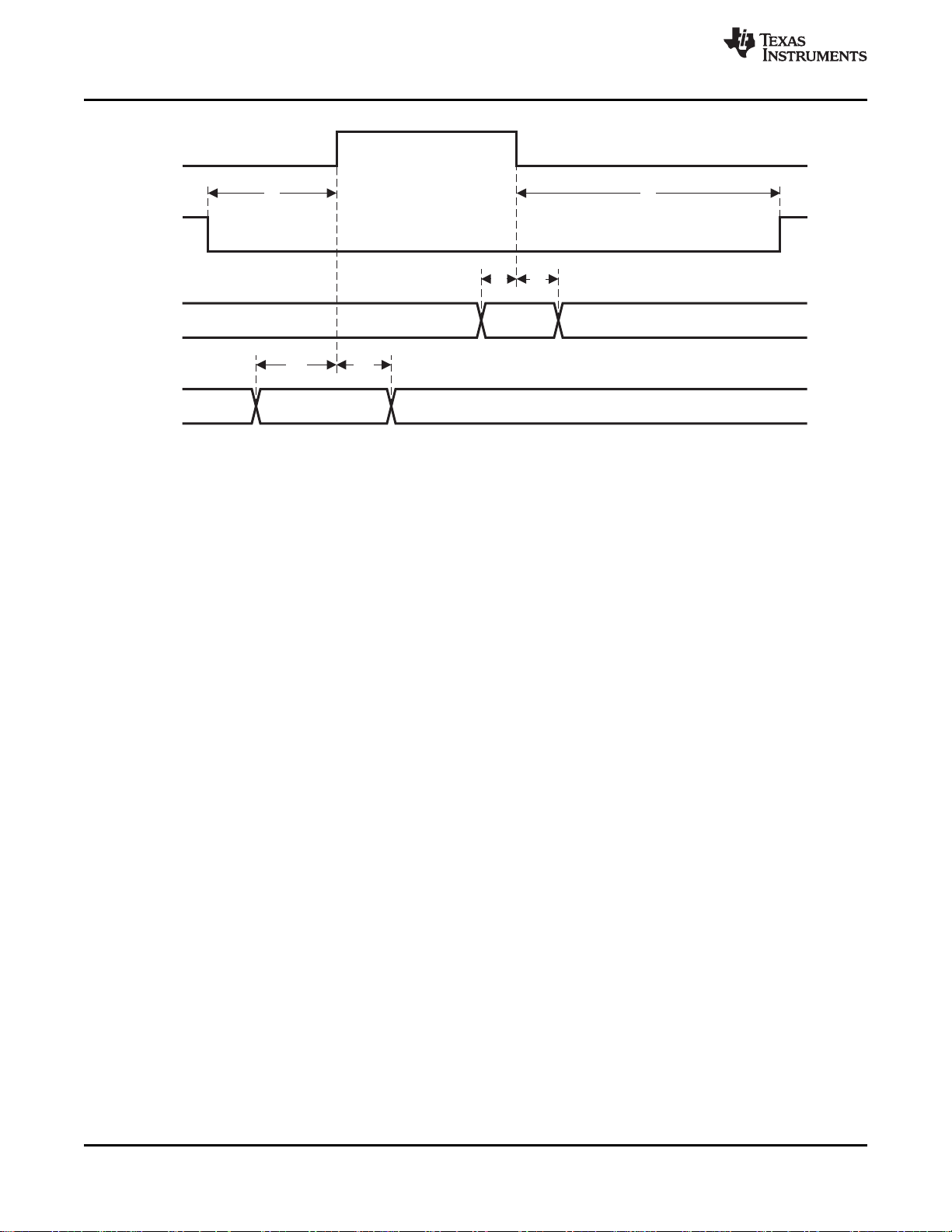
RESET_N
Px.n
T0299-01
1 2
CC2530F32, CC2530F64
CC2530F128, CC2530F256
SWRS081B –APRIL 2009– REVISED FEBRUARY 2011
CONTROL INPUT AC CHARACTERISTICS
TA= –40°C to 125°C, VDD = 2 V to 3.6 V, unless otherwise noted.
PARAMETER TEST CONDITIONS MIN TYP MAX UNIT
System clock, f
t
SYSCLK
RESET_N low duration 1 μs
Interrupt pulse duration 20 ns
= 1/f
SYSCLK
SYSCLK
The undivided system clock is 32 MHz when crystal oscillator is used.
The undivided system clock is 16 MHz when calibrated 16-MHz RC 16 32 MHz
oscillator is used.
See item 1, Figure 1. This is the shortest pulse that is recognized as
a complete reset pin request. Note that shorter pulses may be
recognized but might not lead to complete reset of all modules within
the chip.
See item 2, Figure 1.This is the shortest pulse that is recognized as
an interrupt request.
www.ti.com
Figure 1. Control Input AC Characteristics
12 Submit Documentation Feedback © 2009–2011, Texas Instruments Incorporated
Product Folder Link(s): CC2530F32 CC2530F64 CC2530F128 CC2530F256

SCK
SSN
MOSI
MISO
D0
D1
X
D0
X
t
2
t
4
t
6
t
7
t
5
t
3
X
T0478-01
CC2530F32, CC2530F64
CC2530F128, CC2530F256
www.ti.com
SPI AC CHARACTERISTICS
TA= –40°C to 125°C, VDD = 2 V to 3.6 V
PARAMETER TEST CONDITIONS MIN TYP MAX UNIT
t
SCK period ns
1
SCK duty cycle Master 50%
t
SSN low to SCK ns
2
t
SCK to SSN high ns
3
t
MOSI early out Master, load = 10 pF 7 ns
4
t
MOSI late out Master, load = 10 pF 10 ns
5
t
MISO setup Master 90 ns
6
t
MISO hold Master 10 ns
7
SCK duty cycle Slave 50% ns
t
MOSI setup Slave 35 ns
10
t
MOSI hold Slave 10 ns
11
t
MISO late out Slave, load = 10 pF 95 ns
9
Operating frequency MHz
Master, RX and TX 250
Slave, RX and TX 250
Master 63
Slave 63
Master 63
Slave 63
Master, TX only 8
Master, RX and TX 4
Slave, RX only 8
Slave, RX and TX 4
SWRS081B –APRIL 2009– REVISED FEBRUARY 2011
Figure 2. SPI Master AC Characteristics
© 2009–2011, Texas Instruments Incorporated Submit Documentation Feedback 13
Product Folder Link(s): CC2530F32 CC2530F64 CC2530F128 CC2530F256
T0479-01
SCK
SSN
MOSI
MISO
D0
D1
X
D0
X
t
2
t
3
X
t
8
t
10
t
11
t
9
CC2530F32, CC2530F64
CC2530F128, CC2530F256
SWRS081B –APRIL 2009– REVISED FEBRUARY 2011
Figure 3. SPI Slave AC Characteristics
www.ti.com
14 Submit Documentation Feedback © 2009–2011, Texas Instruments Incorporated
Product Folder Link(s): CC2530F32 CC2530F64 CC2530F128 CC2530F256

Time
DEBUG_CLK
P2_2
t
1
t
2
1/f
clk_dbg
T0436-01
RESET_N
Time
DEBUG_CLK
P2_2
t
3
t
4
t
5
T0437-01
www.ti.com
DEBUG INTERFACE AC CHARACTERISTICS
TA= –40°C to 125°C, VDD = 2 V to 3.6 V, unless otherwise noted.
PARAMETER TEST CONDITIONS MIN TYP MAX UNIT
f
clk_dbg
t
1
t
2
t
3
t
4
t
5
t
6
t
7
t
8
Debug clock frequency (see Figure 4) 12 MHz
Allowed high pulse on clock (see Figure 4) 35 ns
Allowed low pulse on clock (see Figure 4) 35 ns
EXT_RESET_N low to first falling edge on
debug clock (see Figure 5)
Falling edge on clock to EXT_RESET_N high
(see Figure 5)
EXT_RESET_N high to first debug command
(see Figure 5)
Debug data setup (see Figure 6) 2 ns
Debug data hold (see Figure 6) 4 ns
Clock-to-data delay (see Figure 6) Load = 10 pF 30 ns
CC2530F32, CC2530F64
CC2530F128, CC2530F256
SWRS081B –APRIL 2009– REVISED FEBRUARY 2011
167 ns
83 ns
83 ns
Figure 4. Debug Clock – Basic Timing
Figure 5. Data Setup and Hold Timing
© 2009–2011, Texas Instruments Incorporated Submit Documentation Feedback 15
Product Folder Link(s): CC2530F32 CC2530F64 CC2530F128 CC2530F256

Time
DEBUG_ CLK
P2_2
DEBUG_DATA
(to CC253x)
P2_1
DEBUG_DATA
(from CC253x)
P2_1
T0438-01
t
6
t
8
t
7
CC2530F32, CC2530F64
CC2530F128, CC2530F256
SWRS081B –APRIL 2009– REVISED FEBRUARY 2011
www.ti.com
Figure 6. Debug Enable Timing
TIMER INPUTS AC CHARACTERISTICS
TA= –40°C to 125°C, VDD = 2 V to 3.6 V, unless otherwise noted.
PARAMETER TEST CONDITIONS MIN TYP MAX UNIT
Synchronizers determine the shortest input pulse that can be t
Input capture pulse duration recognized. The synchronizers operate at the current system 1.5
clock rate (16 or 32 MHz).
SYSCLK
16 Submit Documentation Feedback © 2009–2011, Texas Instruments Incorporated
Product Folder Link(s): CC2530F32 CC2530F64 CC2530F128 CC2530F256

CC2530
RHA Package
(TopView)
P0_1
RESET_N
P2_3/XOSC32K_Q2
AVDD6
GND RBIAS
30
1
29
2
28
3
27
4
26
5
25
6
24
22
7
9
23
21
8
10
18
20
33
31
17
19
34
32
16
35
15
36
14
37
13
38
12
39
11
40
P0_2
P0_0
AVDD4
P0_3
AVDD1
P0_4
AVDD2
P0_5
RF_N
P0_6
RF_P
P0_7
AVDD3
XOSC_Q1
P1_0
XOSC_Q2
AVDD5
GND
GroundPad
P2_2
P2_4/XOSC32K_Q1
GND
P2_1
GND
P2_0
GND
P1_7
P1_5
P1_6
P1_4
DVDD1
P1_3
P1_1
DCOUPL
P1_2
DVDD2
P0076-02
CC2530F32, CC2530F64
CC2530F128, CC2530F256
www.ti.com
DC CHARACTERISTICS
TA= 25°C, VDD = 3 V, unless otherwise noted.
PARAMETER TEST CONDITIONS MIN TYP MAX UNIT
Logic-0 input voltage 0.5 V
Logic-1 input voltage 2.5 V
Logic-0 input current Input equals 0 V –50 50 nA
Logic-1 input current Input equals VDD –50 50 nA
I/O-pin pullup and pulldown resistors 20 kΩ
Logic-0 output voltage, 4-mA pins Output load 4 mA 0.5 V
Logic-1 output voltage, 4-mA pins Output load 4 mA 2.4 V
Logic-0 output voltage, 20-mA pins Output load 20 mA 0.5 V
Logic-1 output voltage, 20-mA pins Output load 20 mA 2.4 V
DEVICE INFORMATION
PIN DESCRIPTIONS
The CC2530 pinout is shown in Figure 7 and a short description of the pins follows.
SWRS081B –APRIL 2009– REVISED FEBRUARY 2011
NOTE: The exposed ground pad must be connected to a solid ground plane, as this is the ground connection for the chip.
© 2009–2011, Texas Instruments Incorporated Submit Documentation Feedback 17
Product Folder Link(s): CC2530F32 CC2530F64 CC2530F128 CC2530F256
Figure 7. Pinout Top View

CC2530F32, CC2530F64
CC2530F128, CC2530F256
SWRS081B –APRIL 2009– REVISED FEBRUARY 2011
Table 1. Pin Descriptions
PIN NAME PIN PIN TYPE DESCRIPTION
AVDD1 28 Power (analog) 2-V–3.6-V analog power-supply connection
AVDD2 27 Power (analog) 2-V–3.6-V analog power-supply connection
AVDD3 24 Power (analog) 2-V–3.6-V analog power-supply connection
AVDD4 29 Power (analog) 2-V–3.6-V analog power-supply connection
AVDD5 21 Power (analog) 2-V–3.6-V analog power-supply connection
AVDD6 31 Power (analog) 2-V–3.6-V analog power-supply connection
DCOUPL 40 Power (digital) 1.8-V digital power-supply decoupling. Do not use for supplying external circuits.
DVDD1 39 Power (digital) 2-V–3.6-V digital power-supply connection
DVDD2 10 Power (digital) 2-V–3.6-V digital power-supply connection
GND — Ground The ground pad must be connected to a solid ground plane.
GND 1, 2, 3, 4 Unused pins Connect to GND
P0_0 19 Digital I/O Port 0.0
P0_1 18 Digital I/O Port 0.1
P0_2 17 Digital I/O Port 0.2
P0_3 16 Digital I/O Port 0.3
P0_4 15 Digital I/O Port 0.4
P0_5 14 Digital I/O Port 0.5
P0_6 13 Digital I/O Port 0.6
P0_7 12 Digital I/O Port 0.7
P1_0 11 Digital I/O Port 1.0 – 20-mA drive capability
P1_1 9 Digital I/O Port 1.1 – 20-mA drive capability
P1_2 8 Digital I/O Port 1.2
P1_3 7 Digital I/O Port 1.3
P1_4 6 Digital I/O Port 1.4
P1_5 5 Digital I/O Port 1.5
P1_6 38 Digital I/O Port 1.6
P1_7 37 Digital I/O Port 1.7
P2_0 36 Digital I/O Port 2.0
P2_1 35 Digital I/O Port 2.1
P2_2 34 Digital I/O Port 2.2
P2_3/ Digital I/O, Port 2.3/32.768 kHz XOSC
XOSC32K_Q2 Analog I/O
P2_4/ Digital I/O, Port 2.4/32.768 kHz XOSC
XOSC32K_Q1 Analog I/O
RBIAS 30 Analog I/O External precision bias resistor for reference current
RESET_N 20 Digital input Reset, active-low
RF_N 26 RF I/O
RF_P RF I/O
XOSC_Q1 22 Analog I/O 32-MHz crystal oscillator pin 1 or external-clock input
XOSC_Q2 23 Analog I/O 32-MHz crystal oscillator pin 2
33
32
Negative RF input signal to LNA during RX
Negative RF output signal from PA during TX
25 Positive RF input signal to LNA during RX
Positive RF output signal from PA during TX
www.ti.com
18 Submit Documentation Feedback © 2009–2011, Texas Instruments Incorporated
Product Folder Link(s): CC2530F32 CC2530F64 CC2530F128 CC2530F256

RESET
WATCHDOG
TIMER
IRQ CTRL
FLASH CTRL
DEBUG
INTERFACE
CLOCK MUX
and
CALIBRATION
DMA
8051 CPU
CORE
32-MHz
CRYSTAL OSC
32.768-kHz
CRYSTAL OSC
HIGH-
SPEED
RC-OSC
POWER MANAGEMENT CONTROLLER
USART 0
USART 1
TIMER 1 (16-Bit)
TIMER 3 (8-Bit)
TIMER 4 (8-Bit)
TIMER 2
(IEEE 802.15.4 MAC TIMER)
32/64/128/256-KB
FLASH
8-KB SRAM
ON-CHIP VOLTAGE
REGULATOR
POWER-ON RESET
BROWN OUT
VDD (2 V–3.6 V)
DCOUPL
RESET_N
XOSC_Q2
XOSC_Q1
P2_4
P1_7
P0_7
P2_3
P1_6
P0_6
P2_2
P1_5
P0_5
P1_2
P0_2
P2_1
P1_4
P0_4
P1_1
P0_1
P2_0
P1_3
P0_3
P1_0
P0_0
B0301-02
RADIO DATA INTERFACE
CSMA/CA STROBE PROCESSOR
RADIO REGISTERS
MODULATOR
DEMODULATOR
AND AGC
RECEIVE
CHAIN
TRANSMIT
CHAIN
FREQUENCY
SYNTHESIZER
SYNTH
RF_P RF_N
FIFO and FRAME CONTROL
12-BIT
ADC
DS
AES
ENCRYPTION
AND
DECRYPTION
MEMORY
ARBITER
SLEEP TIMER
32-kHz
RC-OSC
I/O CONTROLLER
DIGITAL
ANALOG
MIXED
ANALOG
COMPARATOR
OP-AMP
www.ti.com
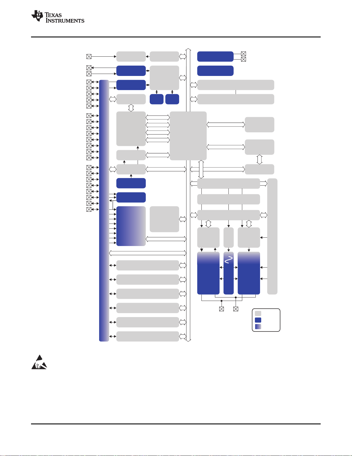
CIRCUIT DESCRIPTION
CC2530F32, CC2530F64
CC2530F128, CC2530F256
SWRS081B –APRIL 2009– REVISED FEBRUARY 2011
© 2009–2011, Texas Instruments Incorporated Submit Documentation Feedback 19
Product Folder Link(s): CC2530F32 CC2530F64 CC2530F128 CC2530F256

CC2530F32, CC2530F64
CC2530F128, CC2530F256
SWRS081B –APRIL 2009– REVISED FEBRUARY 2011
Figure 8. CC2530 Block Diagram
A block diagram of the CC2530 is shown in Figure 8. The modules can be roughly divided into one of three
categories: CPU- and memory-related modules; modules related to peripherals, clocks, and power management;
and radio-related modules. In the following subsections, a short description of each module that appears in
Figure 8 is given.
For more details about the modules and their usage, see the corresponding chapters in the CC253x User's
Guide (SWRU191).
CPU and Memory
The 8051 CPU core used in the CC253x device family is a single-cycle 8051-compatible core. It has three
different memory-access buses (SFR, DATA and CODE/XDATA) with single-cycle access to SFR, DATA, and
the main SRAM. It also includes a debug interface and an 18-input extended interrupt unit.
The interrupt controller services a total of 18 interrupt sources, divided into six interrupt groups, each of which
is associated with one of four interrupt priorities. Any interrupt service request is serviced also when the device is
in idle mode by going back to active mode. Some interrupts can also wake up the device from sleep mode
(power modes 1–3).
The memory arbiter is at the heart of the system, as it connects the CPU and DMA controller with the physical
memories and all peripherals through the SFR bus. The memory arbiter has four memory access points, access
of which can map to one of three physical memories: an 8-KB SRAM, flash memory, and XREG/SFR registers. It
is responsible for performing arbitration and sequencing between simultaneous memory accesses to the same
physical memory.
The 8-KB SRAM maps to the DATA memory space and to parts of the XDATA memory spaces. The 8-KB
SRAM is an ultralow-power SRAM that retains its contents even when the digital part is powered off (power
modes 2 and 3). This is an important feature for low-power applications.
The 32/64/128/256 KB flash block provides in-circuit programmable non-volatile program memory for the
device, and maps into the CODE and XDATA memory spaces. In addition to holding program code and
constants, the non-volatile memory allows the application to save data that must be preserved such that it is
available after restarting the device. Using this feature one can, e.g., use saved network-specific data to avoid
the need for a full start-up and network find-and-join process .
www.ti.com
Clocks and Power Management The digital core and peripherals are powered by a 1.8-V low-dropout voltage regulator. It provides power
management functionality that enables low power operation for long battery life using different power modes.
Five different reset sources exist to reset the device.
Peripherals
The CC2530 includes many different peripherals that allow the application designer to develop advanced
applications.
The debug interface implements a proprietary two-wire serial interface that is used for in-circuit debugging.
Through this debug interface, it is possible to perform an erasure of the entire flash memory, control which
oscillators are enabled, stop and start execution of the user program, execute supplied instructions on the 8051
core, set code breakpoints, and single-step through instructions in the code. Using these techniques, it is
possible to perform in-circuit debugging and external flash programming elegantly.
The device contains flash memory for storage of program code. The flash memory is programmable from the
user software and through the debug interface. The flash controller handles writing and erasing the embedded
flash memory. The flash controller allows page-wise erasure and 4-bytewise programming.
The I/O controller is responsible for all general-purpose I/O pins. The CPU can configure whether peripheral
modules control certain pins or whether they are under software control, and if so, whether each pin is configured
as an input or output and if a pullup or pulldown resistor in the pad is connected. CPU interrupts can be enabled
on each pin individually. Each peripheral that connects to the I/O pins can choose between two different I/O pin
locations to ensure flexibility in various applications.
20 Submit Documentation Feedback © 2009–2011, Texas Instruments Incorporated
Product Folder Link(s): CC2530F32 CC2530F64 CC2530F128 CC2530F256

CC2530F32, CC2530F64
CC2530F128, CC2530F256
www.ti.com
A versatile five-channel DMA controller is available in the system, accesses memory using the XDATA memory
space, and thus has access to all physical memories. Each channel (trigger, priority, transfer mode, addressing
mode, source and destination pointers, and transfer count) is configured with DMA descriptors anywhere in
memory. Many of the hardware peripherals (AES core, flash controller, USARTs, timers, ADC interface) achieve
highly efficient operation by using the DMA controller for data transfers between SFR or XREG addresses and
flash/SRAM.
Timer 1 is a 16-bit timer with timer/counter/PWM functionality. It has a programmable prescaler, a 16-bit period
value, and five individually programmable counter/capture channels, each with a 16-bit compare value. Each of
the counter/capture channels can be used as a PWM output or to capture the timing of edges on input signals. It
can also be configured in IR Generation Mode where it counts Timer 3 periods and the output is ANDed with
the output of Timer 3 to generate modulated consumer IR signals with minimal CPU interaction.
Timer 2 (the MAC Timer) is specially designed for supporting an IEEE 802.15.4 MAC or other time-slotted
protocol in software. The timer has a configurable timer period and a 24-bit overflow counter that can be used to
keep track of the number of periods that have transpired. A 40-bit capture register is also used to record the
exact time at which a start-of-frame delimiter is received/transmitted or the exact time at which transmission
ends, as well as two 16-bit output compare registers and two 24-bit overflow compare registers that can send
various command strobes (start RX, start TX, etc.) at specific times to the radio modules.
Timer 3 and Timer 4 are 8-bit timers with timer/counter/PWM functionality. They have a programmable
prescaler, an 8-bit period value, and one programmable counter channel with an 8-bit compare value. Each of
the counter channels can be used as a PWM output.
The sleep timer is an ultralow-power timer that counts 32-kHz crystal oscillator or 32-kHz RC oscillator periods.
The sleep timer runs continuously in all operating modes except power mode 3 (PM3). Typical applications of
this timer are as a real-time counter or as a wake-up timer to come out of power mode 1 (PM1) or 2 (PM2).
The ADC supports 7 to 12 bits of resolution in a 30 kHz to 4 kHz bandwidth, respectively. DC and audio
conversions with up to eight input channels (Port 0) are possible. The inputs can be selected as single-ended or
differential. The reference voltage can be internal, AVDD, or a single-ended or differential external signal. The
ADC also has a temperature-sensor input channel. The ADC can automate the process of periodic sampling or
conversion over a sequence of channels.
The operational amplifier is intended to provide front-end buffering and gain for the ADC. Both inputs as well as
the output are available on pins, so the feedback network is fully customizable. A chopper-stabilized mode is
available for applications that need good accuracy with high gain.
The ultralow-power analog comparator enables applications to wake up from PM2 or PM3 based on an analog
signal. Both inputs are brought out to pins; the reference voltage must be provided externally. The comparator
output is connected to the I/O controller interrupt detector and can be treated by the MCU as a regular I/O pin
interrupt.
The random-number generator uses a 16-bit LFSR to generate pseudorandom numbers, which can be read by
the CPU or used directly by the command strobe processor. It can be seeded with random data from noise in the
radio ADC.
The AES encryption/decryption core allows the user to encrypt and decrypt data using the AES algorithm with
128-bit keys. The core is able to support the AES operations required by IEEE 802.15.4 MAC security, the
ZigBee network layer, and the application layer.
A built-in watchdog timer allows the CC2530 to reset itself in case the firmware hangs. When enabled by
software, the watchdog timer must be cleared periodically; otherwise, it resets the device when it times out. It can
alternatively be configured for use as a general 32-kHz timer.
USART 0 and USART 1 are each configurable as either a SPI master/slave or a UART. They provide double
buffering on both RX and TX and hardware flow control and are thus well suited to high-throughput full-duplex
applications. Each has its own high-precision baud-rate generator, thus leaving the ordinary timers free for other
uses.
SWRS081B –APRIL 2009– REVISED FEBRUARY 2011
© 2009–2011, Texas Instruments Incorporated Submit Documentation Feedback 21
Product Folder Link(s): CC2530F32 CC2530F64 CC2530F128 CC2530F256

T − Temperature − °C
32
33
34
35
36
−40 0 40 80 120
TX Current − mA
G002
T − Temperature − °C
22
23
24
25
26
27
28
−40 0 40 80 120
RX Current − mA
G001
V
CC
− Supply Voltage − V
24.0
24.5
25.0
25.5
26.0
2.0 2.4 2.8 3.2 3.6
RX Current − mA
G003
V
CC
− Supply Voltage − V
33.6
33.8
34.0
34.2
34.4
2.0 2.4 2.8 3.2 3.6
TX Current − mA
G004
CC2530F32, CC2530F64
CC2530F128, CC2530F256
SWRS081B –APRIL 2009– REVISED FEBRUARY 2011
Radio
The CC2530 features an IEEE 802.15.4-compliant radio transceiver. The RF core controls the analog radio
modules. In addition, it provides an interface between the MCU and the radio which makes it possible to issue
commands, read status, and automate and sequence radio events. The radio also includes a packet-filtering and
address-recognition module.
TYPICAL CHARACTERISTICS
RX CURRENT (–100 dBm INPUT) TX CURRENT (TXPOWER = 0xF5)
vs vs
TEMPERATURE TEMPERATURE
www.ti.com
RX CURRENT (–100 dBm INPUT) TX CURRENT (TXPOWER = 0xF5)
SUPPLY VOLTAGE SUPPLY VOLTAGE
Figure 11. Figure 12.
22 Submit Documentation Feedback © 2009–2011, Texas Instruments Incorporated
Product Folder Link(s): CC2530F32 CC2530F64 CC2530F128 CC2530F256
Figure 9. Figure 10.
vs vs

f − Frequency − MHz
3.5
4.0
4.5
5.0
5.5
6.0
2394 2414 2434 2454 2474 2494
P
O
− Output Power − dBm
G005
Interferer Frequency − MHz
−25
0
25
50
75
2400 2420 2440 2460 2480
Interferer Rejection − dB
G006
T − Temperature − °C
−99
−98
−97
−96
−95
−94
−93
−92
−40 0 40 80 120
Sensitivity − dBm
G007
T − Temperature − °C
−2
0
2
4
6
8
−40 0 40 80 120
P
O
− Output Power − dBm
G008
www.ti.com
TYPICAL CHARACTERISTICS (continued)
OUTPUT POWER (TXPOWER = 0xF5)
vs
FREQUENCY MHz)
CC2530F32, CC2530F64
CC2530F128, CC2530F256
SWRS081B –APRIL 2009– REVISED FEBRUARY 2011
INTERFERER REJECTION (802.15.4 INTERFERER)
vs
INTERFERER FREQUENCY (CARRIER AT –82 dBm, 2440
Figure 13. Figure 14.
SENSITIVITY OUTPUT POWER (TXPOWER = 0xF5)
TEMPERATURE TEMPERATURE
© 2009–2011, Texas Instruments Incorporated Submit Documentation Feedback 23
Figure 15. Figure 16.
Product Folder Link(s): CC2530F32 CC2530F64 CC2530F128 CC2530F256
vs vs

V
CC
− Supply Voltage − V
4.0
4.2
4.4
4.6
4.8
5.0
2.0 2.4 2.8 3.2 3.6
P
O
− Output Power − dBm
G009
V
CC
− Supply Voltage − V
−100
−99
−98
−97
−96
−95
−94
2.0 2.4 2.8 3.2 3.6
Sensitivity − dBm
G010
CC2530F32, CC2530F64
CC2530F128, CC2530F256
SWRS081B –APRIL 2009– REVISED FEBRUARY 2011
TYPICAL CHARACTERISTICS (continued)
OUTPUT POWER (TXPOWER = 0xF5) SENSITIVITY
vs vs
SUPPLY VOLTAGE SUPPLY VOLTAGE
www.ti.com
Figure 17. Figure 18.
Table 2. Recommended Output Power Settings
(1)
TXPOWER Register Setting Typical Output Power (dBm) Typical Current Consumption (mA)
0xF5 4.5 34
0xE5 2.5 31
0xD5 1 29
0xC5 –0.5 28
0xB5 –1.5 27
0xA5 –3 27
0x95 –4 26
0x85 –6 26
0x75 –8 25
0x65 –10 25
0x55 –12 25
0x45 –14 25
0x35 –16 25
0x25 –18 24
0x15 –20 24
0x05 –22 23
0x05 and TXCTRL = 0x09 –28 23
(1) Measured on Texas Instruments CC2530 EM reference design with TA= 25°C, VDD = 3 V and fc= 2440 MHz, unless otherwise noted.
See References, Item 1, for recommended register settings.
24 Submit Documentation Feedback © 2009–2011, Texas Instruments Incorporated
Product Folder Link(s): CC2530F32 CC2530F64 CC2530F128 CC2530F256

R301
C251
C261
C262
C252
C253
L252
L261
XTAL1
C221
C231
XTAL2
C321
C331
C401
Optional 32-kHz Crystal
1 GND
2 GND
3 GND
4 GND
5 P1_5
CC2530
DIE ATTACH PAD
10 DVDD2
9 P1_1
8 P1_2
7 P1_3
6 P1_4
RBIAS 30
AVDD4 29
AVDD1 28
AVDD2 27
RF_N 26
AVDD5 21
XOSC_Q1 22
XOSC_Q2 23
AVDD3 24
RF_P 25
11 P1_0
12 P0_7
13 P0_6
14 P0_5
15 P0_4
20 RESET_N
19 P0_0
18 P0_1
17 P0_2
16 P0_3
DCOUPL 40
DVDD1 39
P1_6 38
P1_7 37
P2_0 36
AVDD6 31
P2_4/XOSC32K_Q1 32
P2_3/XOSC32K_Q2 33
P2_2 34
P2_1 35
2-Vto3.6-V
PowerSupply
PowerSupplyDecouplingCapacitorsareNotShown
DigitalI/ONotConnected
Antenna
(50 )W
S0383-01
CC2530F32, CC2530F64
CC2530F128, CC2530F256
www.ti.com
APPLICATION INFORMATION
Few external components are required for the operation of the CC2530. A typical application circuit is shown in
Figure 19. Typical values and description of external components are shown in Table 3.
SWRS081B –APRIL 2009– REVISED FEBRUARY 2011
Figure 19. CC2530 Application Circuit
Table 3. Overview of External Components (Excluding Supply Decoupling Capacitors)
Component Description Value
C251 Part of the RF matching network 18 pF
C261 Part of the RF matching network 18 pF
L252 Part of the RF matching network 2 nH
L261 Part of the RF matching network 2 nH
C262 Part of the RF matching network 1 pF
C252 Part of the RF matching network 1 pF
C253 Part of the RF matching network 2.2 pF
C331 32kHz xtal loading capacitor 15 pF
C321 32kHz xtal loading capacitor 15 pF
C231 32MHz xtal loading capacitor 27 pF
C221 32MHz xtal loading capacitor 27 pF
C401 Decoupling capacitor for the internal digital regulator 1 μF
© 2009–2011, Texas Instruments Incorporated Submit Documentation Feedback 25
Product Folder Link(s): CC2530F32 CC2530F64 CC2530F128 CC2530F256

L parasitic
221 231
1
C C
1 1
C C
= +
+
L parasitic
321 331
1
C C
1 1
C C
= +
+
CC2530F32, CC2530F64
CC2530F128, CC2530F256
SWRS081B –APRIL 2009– REVISED FEBRUARY 2011
Table 3. Overview of External Components (Excluding Supply Decoupling Capacitors) (continued)
Component Description Value
R301 Resistor used for internal biasing 56 kΩ
Input/Output Matching
When using an unbalanced antenna such as a monopole, a balun should be used to optimize performance. The
balun can be implemented using low-cost discrete inductors and capacitors. The recommended balun shown
consists of C262, L261, C252, and L252.
If a balanced antenna such as a folded dipole is used, the balun can be omitted.
Crystal
An external 32-MHz crystal, XTAL1, with two loading capacitors (C221 and C231) is used for the 32-MHz crystal
oscillator. See the 32-MHz Crystal Oscillator section for details. The load capacitance seen by the 32-MHz
crystal is given by:
XTAL2 is an optional 32.768-kHz crystal, with two loading capacitors (C321 and C331) used for the 32.768-kHz
crystal oscillator. The 32.768-kHz crystal oscillator is used in applications where both very low sleep-current
consumption and accurate wake-up times are needed. The load capacitance seen by the 32.768-kHz crystal is
given by:
www.ti.com
(1)
(2)
A series resistor may be used to comply with the ESR requirement.
On-Chip 1.8-V Voltage-Regulator Decoupling
The 1.8-V on-chip voltage regulator supplies the 1.8-V digital logic. This regulator requires a decoupling capacitor
(C401) for stable operation.
Power-Supply Decoupling and Filtering
Proper power-supply decoupling must be used for optimum performance. The placement and size of the
decoupling capacitors and the power supply filtering are very important to achieve the best performance in an
application. TI provides a compact reference design that should be followed very closely.
References
1. IEEE Std. 802.15.4-2006: Wireless Medium Access Control (MAC) and Physical Layer (PHY) Specifications
for Low-Rate Wireless Personal Area Networks (LR-WPANs)
http://standards.ieee.org/getieee802/download/802.15.4-2006.pdf
2. CC253x User's Guide – CC253x System-on-Chip Solution for 2.4 GHz IEEE 802.15.4 and ZigBee
Applications (SWRU191)
Additional Information
Texas Instruments offers a wide selection of cost-effective, low-power RF solutions for proprietary and
standard-based wireless applications for use in industrial and consumer applications. Our selection includes RF
transceivers, RF transmitters, RF front ends, and System-on-Chips as well as various software solutions for the
sub-1- and 2.4-GHz frequency bands.
26 Submit Documentation Feedback © 2009–2011, Texas Instruments Incorporated
Product Folder Link(s): CC2530F32 CC2530F64 CC2530F128 CC2530F256

CC2530F32, CC2530F64
CC2530F128, CC2530F256
www.ti.com
In addition, Texas Instruments provides a large selection of support collateral such as development tools,
technical documentation, reference designs, application expertise, customer support, third-party and university
programs.
The Low-Power RF E2E Online Community provides technical support forums, videos and blogs, and the chance
to interact with fellow engineers from all over the world.
With a broad selection of product solutions, end application possibilities, and a range of technical support, Texas
Instruments offers the broadest low-power RF portfolio. We make RF easy!
The following subsections point to where to find more information.
Texas Instruments Low-Power RF Web Site
Texas Instruments’ Low-Power RF Web site has all our latest products, application and design notes, FAQ
section, news and events updates, and much more. Just go to www.ti.com/lprf.
Low-Power RF Online Community
• Forums, videos, and blogs
• RF design help
• E2E interaction
Join us today at www.ti.com/lprf-forum.
SWRS081B –APRIL 2009– REVISED FEBRUARY 2011
Texas Instruments Low-Power RF Developer Network
Texas Instruments has launched an extensive network of low-power RF development partners to help customers
speed up their application development. The network consists of recommended companies, RF consultants, and
independent design houses that provide a series of hardware module products and design services, including:
• RF circuit, low-power RF, and ZigBee design services
• Low-power RF and ZigBee module solutions and development tools
• RF certification services and RF circuit manufacturing
Need help with modules, engineering services or development tools?
Search the Low-Power RF Developer Network tool to find a suitable partner. www.ti.com/lprfnetwork
Low-Power RF eNewsletter
The Low-Power RF eNewsletter keeps you up-to-date on new products, news releases, developers’ news, and
other news and events associated with low-power RF products from TI. The Low-Power RF eNewsletter articles
include links to get more online information.
Sign up today on www.ti.com/lprfnewsletter
© 2009–2011, Texas Instruments Incorporated Submit Documentation Feedback 27
Product Folder Link(s): CC2530F32 CC2530F64 CC2530F128 CC2530F256

CC2530F32, CC2530F64
CC2530F128, CC2530F256
SWRS081B –APRIL 2009– REVISED FEBRUARY 2011
REVISION HISTORY
Changes from Revision A (November 2010) to Revision B Page
• Changed recommendation for single-crystal implementations to asynchronous networks .................................................. 1
• Added op-amp and comparator to peripherals list ................................................................................................................ 1
• Revised block diagram ......................................................................................................................................................... 3
• Added number of erase cycles and page size for flash ........................................................................................................ 5
• Updated ESR for 32 kHz crystal ........................................................................................................................................... 8
• Updated voltage coefficient for temperature sensor ............................................................................................................. 9
• Added tables for op-amp and comparator to the Electrical Characteristics section ........................................................... 10
• Changed SPI AC characteristics SSN low from SCK negative edge to SCK positive edge and split into separate
master and slave tables. ..................................................................................................................................................... 13
• Revised block diagram ....................................................................................................................................................... 19
• Corrected description of Timer 2 (MAC Timer) ................................................................................................................... 21
• Improved readability of sleep timer description. ................................................................................................................. 21
• Added the operational amplifier and the ultralow-power analog comparator paragraphs from the SWRS084 after The
ADC supports... channels paragraph .................................................................................................................................. 21
• Removed sentence that pseudorandom data can be used for security ............................................................................. 21
www.ti.com
28 Submit Documentation Feedback © 2009–2011, Texas Instruments Incorporated
Product Folder Link(s): CC2530F32 CC2530F64 CC2530F128 CC2530F256

PACKAGE OPTION ADDENDUM
www.ti.com
6-Oct-2010
PACKAGING INFORMATION
Orderable Device
CC2530F128RHAR ACTIVE VQFN RHA 40 2500 Green (RoHS
CC2530F128RHAT ACTIVE VQFN RHA 40 250 Green (RoHS
CC2530F256RHAR ACTIVE VQFN RHA 40 2500 Green (RoHS
CC2530F256RHAT ACTIVE VQFN RHA 40 250 Green (RoHS
CC2530F32RHAR ACTIVE VQFN RHA 40 2500 Green (RoHS
CC2530F32RHAT ACTIVE VQFN RHA 40 250 Green (RoHS
CC2530F64RHAR ACTIVE VQFN RHA 40 2500 Green (RoHS
CC2530F64RHAT ACTIVE VQFN RHA 40 250 Green (RoHS
(1)
The marketing status values are defined as follows:
ACTIVE: Product device recommended for new designs.
LIFEBUY: TI has announced that the device will be discontinued, and a lifetime-buy period is in effect.
NRND: Not recommended for new designs. Device is in production to support existing customers, but TI does not recommend using this part in a new design.
PREVIEW: Device has been announced but is not in production. Samples may or may not be available.
OBSOLETE: TI has discontinued the production of the device.
Status
(1)
Package Type Package
Drawing
Pins Package Qty
Eco Plan
& no Sb/Br)
& no Sb/Br)
& no Sb/Br)
& no Sb/Br)
& no Sb/Br)
& no Sb/Br)
& no Sb/Br)
& no Sb/Br)
(2)
Lead/
Ball Finish
CU NIPDAU Level-3-260C-168 HR Purchase Samples
CU NIPDAU Level-3-260C-168 HR Request Free Samples
CU NIPDAU Level-3-260C-168 HR Purchase Samples
CU NIPDAU Level-3-260C-168 HR Request Free Samples
CU NIPDAU Level-3-260C-168 HR Purchase Samples
CU NIPDAU Level-3-260C-168 HR Request Free Samples
CU NIPDAU Level-3-260C-168 HR Purchase Samples
CU NIPDAU Level-3-260C-168 HR Request Free Samples
MSL Peak Temp
(3)
Samples
(Requires Login)
(2)
Eco Plan - The planned eco-friendly classification: Pb-Free (RoHS), Pb-Free (RoHS Exempt), or Green (RoHS & no Sb/Br) - please check http://www.ti.com/productcontent for the latest availability
information and additional product content details.
TBD: The Pb-Free/Green conversion plan has not been defined.
Pb-Free (RoHS): TI's terms "Lead-Free" or "Pb-Free" mean semiconductor products that are compatible with the current RoHS requirements for all 6 substances, including the requirement that
lead not exceed 0.1% by weight in homogeneous materials. Where designed to be soldered at high temperatures, TI Pb-Free products are suitable for use in specified lead-free processes.
Pb-Free (RoHS Exempt): This component has a RoHS exemption for either 1) lead-based flip-chip solder bumps used between the die and package, or 2) lead-based die adhesive used between
the die and leadframe. The component is otherwise considered Pb-Free (RoHS compatible) as defined above.
Green (RoHS & no Sb/Br): TI defines "Green" to mean Pb-Free (RoHS compatible), and free of Bromine (Br) and Antimony (Sb) based flame retardants (Br or Sb do not exceed 0.1% by weight
in homogeneous material)
(3)
MSL, Peak Temp. -- The Moisture Sensitivity Level rating according to the JEDEC industry standard classifications, and peak solder temperature.
Addendum-Page 1

PACKAGE OPTION ADDENDUM
www.ti.com
Important Information and Disclaimer:The information provided on this page represents TI's knowledge and belief as of the date that it is provided. TI bases its knowledge and belief on information
provided by third parties, and makes no representation or warranty as to the accuracy of such information. Efforts are underway to better integrate information from third parties. TI has taken and
continues to take reasonable steps to provide representative and accurate information but may not have conducted destructive testing or chemical analysis on incoming materials and chemicals.
TI and TI suppliers consider certain information to be proprietary, and thus CAS numbers and other limited information may not be available for release.
6-Oct-2010
In no event shall TI's liability arising out of such information exceed the total purchase price of the TI part(s) at issue in this document sold by TI to Customer on an annual basis.
Addendum-Page 2

PACKAGE MATERIALS INFORMATION
www.ti.com 16-Feb-2012
TAPE AND REEL INFORMATION
*All dimensions are nominal
Device Package
CC2530F128RHAR VQFN RHA 40 2500 330.0 16.4 6.3 6.3 1.5 12.0 16.0 Q2
CC2530F128RHAT VQFN RHA 40 250 330.0 16.4 6.3 6.3 1.5 12.0 16.0 Q2
CC2530F256RHAR VQFN RHA 40 2500 330.0 16.4 6.3 6.3 1.5 12.0 16.0 Q2
CC2530F256RHAT VQFN RHA 40 250 330.0 16.4 6.3 6.3 1.5 12.0 16.0 Q2
CC2530F32RHAR VQFN RHA 40 2500 330.0 16.4 6.3 6.3 1.5 12.0 16.0 Q2
CC2530F32RHAT VQFN RHA 40 250 330.0 16.4 6.3 6.3 1.5 12.0 16.0 Q2
CC2530F64RHAR VQFN RHA 40 2500 330.0 16.4 6.3 6.3 1.5 12.0 16.0 Q2
CC2530F64RHAT VQFN RHA 40 250 330.0 16.4 6.3 6.3 1.5 12.0 16.0 Q2
Type
Package
Drawing
Pins SPQ Reel
Diameter
(mm)
Reel
Width
W1 (mm)
A0
(mm)B0(mm)K0(mm)P1(mm)W(mm)
Pin1
Quadrant
Pack Materials-Page 1

PACKAGE MATERIALS INFORMATION
www.ti.com 16-Feb-2012
*All dimensions are nominal
Device Package Type Package Drawing Pins SPQ Length (mm) Width (mm) Height (mm)
CC2530F128RHAR VQFN RHA 40 2500 336.6 336.6 28.6
CC2530F128RHAT VQFN RHA 40 250 336.6 336.6 28.6
CC2530F256RHAR VQFN RHA 40 2500 336.6 336.6 28.6
CC2530F256RHAT VQFN RHA 40 250 336.6 336.6 28.6
CC2530F32RHAR VQFN RHA 40 2500 336.6 336.6 28.6
CC2530F32RHAT VQFN RHA 40 250 336.6 336.6 28.6
CC2530F64RHAR VQFN RHA 40 2500 336.6 336.6 28.6
CC2530F64RHAT VQFN RHA 40 250 336.6 336.6 28.6
Pack Materials-Page 2


IMPORTANT NOTICE
Texas Instruments Incorporated and its subsidiaries (TI) reserve the right to make corrections, modifications, enhancements, improvements,
and other changes to its products and services at any time and to discontinue any product or service without notice. Customers should
obtain the latest relevant information before placing orders and should verify that such information is current and complete. All products are
sold subject to TI’s terms and conditions of sale supplied at the time of order acknowledgment.
TI warrants performance of its hardware products to the specifications applicable at the time of sale in accordance with TI’s standard
warranty. Testing and other quality control techniques are used to the extent TI deems necessary to support this warranty. Except where
mandated by government requirements, testing of all parameters of each product is not necessarily performed.
TI assumes no liability for applications assistance or customer product design. Customers are responsible for their products and
applications using TI components. To minimize the risks associated with customer products and applications, customers should provide
adequate design and operating safeguards.
TI does not warrant or represent that any license, either express or implied, is granted under any TI patent right, copyright, mask work right,
or other TI intellectual property right relating to any combination, machine, or process in which TI products or services are used. Information
published by TI regarding third-party products or services does not constitute a license from TI to use such products or services or a
warranty or endorsement thereof. Use of such information may require a license from a third party under the patents or other intellectual
property of the third party, or a license from TI under the patents or other intellectual property of TI.
Reproduction of TI information in TI data books or data sheets is permissible only if reproduction is without alteration and is accompanied
by all associated warranties, conditions, limitations, and notices. Reproduction of this information with alteration is an unfair and deceptive
business practice. TI is not responsible or liable for such altered documentation. Information of third parties may be subject to additional
restrictions.
Resale of TI products or services with statements different from or beyond the parameters stated by TI for that product or service voids all
express and any implied warranties for the associated TI product or service and is an unfair and deceptive business practice. TI is not
responsible or liable for any such statements.
TI products are not authorized for use in safety-critical applications (such as life support) where a failure of the TI product would reasonably
be expected to cause severe personal injury or death, unless officers of the parties have executed an agreement specifically governing
such use. Buyers represent that they have all necessary expertise in the safety and regulatory ramifications of their applications, and
acknowledge and agree that they are solely responsible for all legal, regulatory and safety-related requirements concerning their products
and any use of TI products in such safety-critical applications, notwithstanding any applications-related information or support that may be
provided by TI. Further, Buyers must fully indemnify TI and its representatives against any damages arising out of the use of TI products in
such safety-critical applications.
TI products are neither designed nor intended for use in military/aerospace applications or environments unless the TI products are
specifically designated by TI as military-grade or "enhanced plastic." Only products designated by TI as military-grade meet military
specifications. Buyers acknowledge and agree that any such use of TI products which TI has not designated as military-grade is solely at
the Buyer's risk, and that they are solely responsible for compliance with all legal and regulatory requirements in connection with such use.
TI products are neither designed nor intended for use in automotive applications or environments unless the specific TI products are
designated by TI as compliant with ISO/TS 16949 requirements. Buyers acknowledge and agree that, if they use any non-designated
products in automotive applications, TI will not be responsible for any failure to meet such requirements.
Following are URLs where you can obtain information on other Texas Instruments products and application solutions:
Products Applications
Audio www.ti.com/audio Automotive and Transportation www.ti.com/automotive
Amplifiers amplifier.ti.com Communications and Telecom www.ti.com/communications
Data Converters dataconverter.ti.com Computers and Peripherals www.ti.com/computers
DLP® Products www.dlp.com Consumer Electronics www.ti.com/consumer-apps
DSP dsp.ti.com Energy and Lighting www.ti.com/energy
Clocks and Timers www.ti.com/clocks Industrial www.ti.com/industrial
Interface interface.ti.com Medical www.ti.com/medical
Logic logic.ti.com Security www.ti.com/security
Power Mgmt power.ti.com Space, Avionics and Defense www.ti.com/space-avionics-defense
Microcontrollers microcontroller.ti.com Video and Imaging www.ti.com/video
RFID www.ti-rfid.com
OMAP Mobile Processors www.ti.com/omap
Wireless Connectivity www.ti.com/wirelessconnectivity
TI E2E Community Home Page e2e.ti.com
Mailing Address: Texas Instruments, Post Office Box 655303, Dallas, Texas 75265
Copyright © 2012, Texas Instruments Incorporated
 Loading...