

CC2510Fx / CC2511Fx
SWRS055D Page 1 of 243
Low-Power SoC (System-on-Chip) with MCU, Memory,
2.4 GHz RF Transceiver, and USB Controller
Applications
• 2400-2483.5 MHz ISM/SRD band systems
• Consumer electronics
• Wireless keyboard and mouse
• Wireless voice-quality audio
• RF enabled remote controls
• Wireless sports and leisure equipment
• Low power telemetry
•
CC2511Fx
: USB dongles
Product Description
The
CC2510Fx/CC2511Fx
is a true low-cost 2.4
GHz system-on-chip (SoC) designed for lowpower wireless applications. The
CC2510Fx/CC2511Fx
combines the excellent
performance of the state-of-the-art RF
transceiver CC2500 with an industry-standard
enhanced 8051 MCU, up to 32 kB of in-system
programmable flash memory and 4 kB of
RAM, and many other powerful features. The
small 6x6 mm package makes it very suited
for applications with size limitations.
The
CC2510Fx/CC2511Fx
is highly suited for
systems where very low power consumption is
required. This is ensured by several advanced
low-power operating modes. The
CC2511Fx
adds a full-speed USB controller to the feature
set of the
CC2510Fx
. Interfacing to a PC using
the USB interface is quick and easy, and the
high data rate (12 Mbps) of the USB interface
avoids the bottlenecks of RS-232 or low-speed
USB interfaces.
Key Features
• Radio
o High-performance RF transceiver based on
the market-leading CC2500
o Excellent receiver selectivity and blocking
performance
o High sensitivity (-103 dBm at 2.4 kBaud)
o Programmable data rate up to 500 kBaud
o Programmable output power up to 1 dBm for
all supported frequencies
o Frequency range: 2400 – 2483.5 MHz
o Digital RSSI / LQI support
• Current Consumption
o Low current consumption (RX: 17.1 mA @
2.4 kBaud, TX: 18.5 mA @ -6 dBm output
power)
o 0.3 µA in PM3 (the operating mode with the
lowest power consumption)
• MCU, Memory, and Peripherals
o High performance and low power 8051
microcontroller core.
o 8/16/32 kB in-system programmable flash,
and 1/2/4 kB RAM
o Full-Speed USB Controller with 1 kB USB
FIFO (
CC2511Fx
)
o I
2
S interface
o 7-12 bit ADC with up to eight inputs
o 128-bit AES security coprocessor
o Powerful DMA functionality
o Two USARTs
o 16-bit timer with DSM mode
o Three 8-bit timers
o Hardware debug support
o 21 (
CC2510Fx
) or 19 (
CC2511Fx
) GPIO pins
• General
o Wide supply voltage range (2.0V – 3.6V)
o Green package: RoHS compliant and no
antimony or bromine, 6x6mm QLP36

C2510Fx / CC2511Fx
SWRS055D Page 2 of 243
Table of Contents
1 ABBREVIATIONS.................................................................................................................................... 4
2 REGISTER CONVENTIONS.................................................................................................................. 5
3 KEY FEATURES (IN MORE DETAILS) ..............................................................................................6
3.1 HIGH-PERFORMANCE AND LOW-POWER 8051-COMPATIBLE MICROCONTROLLER....................................... 6
3.2 8/16/32 KB NON-VOLATILE PROGRAM MEMORY AND 1/2/4 KB DATA MEMORY......................................... 6
3.3 FULL-SPEED USB CONTROLLER (
CC2511F
X
)................................................................................................ 6
3.4 I2S INTERFACE.............................................................................................................................................. 6
3.5 HARDWARE AES ENCRYPTION/DECRYPTION............................................................................................... 6
3.6 PERIPHERAL FEATURES ................................................................................................................................6
3.7 LOW POWER ................................................................................................................................................. 6
3.8 2.4 GHZ RADIO WITH BASEBAND MODEM ................................................................................................... 7
4 ABSOLUTE MAXIMUM RATINGS...................................................................................................... 8
5 OPERATING CONDITIONS ..................................................................................................................8
5.1
CC2510F
X
OPERATING CONDITIONS .............................................................................................................. 8
5.2
CC2511F
X
OPERATING CONDITIONS .............................................................................................................. 8
6 GENERAL CHARACTERISTICS.......................................................................................................... 9
7 ELECTRICAL SPECIFICATIONS ...................................................................................................... 10
7.1 CURRENT CONSUMPTION ........................................................................................................................... 10
7.2 RF RECEIVE SECTION ................................................................................................................................. 13
7.3 RF TRANSMIT SECTION ..............................................................................................................................15
7.4 CRYSTAL OSCILLATORS ............................................................................................................................. 16
7.5 32.768 KHZ CRYSTAL OSCILLATOR ........................................................................................................... 17
7.6 LOW POWER RC OSCILLATOR.................................................................................................................... 18
7.7 HIGH SPEED RC OSCILLATOR .................................................................................................................... 18
7.8 FREQUENCY SYNTHESIZER CHARACTERISTICS ........................................................................................... 19
7.9 ANALOG TEMPERATURE SENSOR ............................................................................................................... 19
7.10 7-12 BIT ADC............................................................................................................................................. 20
7.11 CONTROL AC CHARACTERISTICS ............................................................................................................... 21
7.12 SPI AC CHARACTERISTICS......................................................................................................................... 22
7.13 DEBUG INTERFACE AC CHARACTERISTICS ................................................................................................ 23
7.14 PORT OUTPUTS AC CHARACTERISTICS ...................................................................................................... 24
7.15 TIMER INPUTS AC CHARACTERISTICS ........................................................................................................24
7.16 DC CHARACTERISTICS ............................................................................................................................... 24
8 PIN AND I/O PORT CONFIGURATION ............................................................................................ 26
9 CIRCUIT DESCRIPTION ..................................................................................................................... 30
9.1 CPU AND PERIPHERALS ............................................................................................................................. 31
9.2 RADIO ........................................................................................................................................................ 33
10 APPLICATION CIRCUIT..................................................................................................................... 33
10.1 BIAS RESISTOR ........................................................................................................................................... 33
10.2 BALUN AND RF MATCHING........................................................................................................................ 33
10.3 CRYSTAL .................................................................................................................................................... 34
10.4 USB (
CC2511F
X
) .........................................................................................................................................34
10.5 POWER SUPPLY DECOUPLING ..................................................................................................................... 34
10.6 PCB LAYOUT RECOMMENDATIONS............................................................................................................ 37
11 8051 CPU.................................................................................................................................................. 38
11.1 8051 INTRODUCTION ..................................................................................................................................38
11.2 MEMORY ....................................................................................................................................................38
11.3 CPU REGISTERS .........................................................................................................................................52
11.4 INSTRUCTION SET SUMMARY ..................................................................................................................... 54
11.5 INTERRUPTS................................................................................................................................................ 58
12 DEBUG INTERFACE............................................................................................................................. 68
12.1 DEBUG MODE............................................................................................................................................. 68
12.2 DEBUG COMMUNICATION...........................................................................................................................68
12.3 DEBUG LOCK BIT ....................................................................................................................................... 69
12.4 DEBUG COMMANDS.................................................................................................................................... 70

C2510Fx / CC2511Fx
SWRS055D Page 3 of 243
13 PERIPHERALS....................................................................................................................................... 74
13.1 POWER MANAGEMENT AND CLOCKS.......................................................................................................... 74
13.2 RESET......................................................................................................................................................... 81
13.3 FLASH CONTROLLER .................................................................................................................................. 82
13.4 I/O PORTS................................................................................................................................................... 88
13.5 DMA CONTROLLER ................................................................................................................................... 99
13.6 16-BIT TIMER, TIMER 1............................................................................................................................. 111
13.7 MAC TIMER (TIMER 2) ............................................................................................................................123
13.8 SLEEP TIMER ............................................................................................................................................ 125
13.9 8-BIT TIMERS, TIMER 3 AND TIMER 4 .......................................................................................................129
13.10 ADC......................................................................................................................................................... 140
13.11 RANDOM NUMBER GENERATOR ............................................................................................................... 146
13.12 AES COPROCESSOR.................................................................................................................................. 147
13.13 WATCHDOG TIMER................................................................................................................................... 150
13.14 USART .................................................................................................................................................... 152
13.15 I2S ............................................................................................................................................................ 163
13.16 USB CONTROLLER ...................................................................................................................................170
14 RADIO.................................................................................................................................................... 187
14.1 COMMAND STROBES ................................................................................................................................187
14.2 RADIO REGISTERS ....................................................................................................................................189
14.3 INTERRUPTS.............................................................................................................................................. 189
14.4 TX/RX DATA TRANSFER ......................................................................................................................... 191
14.5 DATA RATE PROGRAMMING..................................................................................................................... 192
14.6 RECEIVER CHANNEL FILTER BANDWIDTH................................................................................................ 192
14.7 DEMODULATOR, SYMBOL SYNCHRONIZER, AND DATA DECISION ............................................................ 193
14.8 PACKET HANDLING HARDWARE SUPPORT ............................................................................................... 194
14.9 MODULATION FORMATS........................................................................................................................... 197
14.10 RECEIVED SIGNAL QUALIFIERS AND LINK QUALITY INFORMATION......................................................... 198
14.11 FORWARD ERROR CORRECTION WITH INTERLEAVING.............................................................................. 202
14.12 RADIO CONTROL ...................................................................................................................................... 203
14.13 FREQUENCY PROGRAMMING .................................................................................................................... 206
14.14 VCO......................................................................................................................................................... 207
14.15 OUTPUT POWER PROGRAMMING .............................................................................................................. 207
14.16 SELECTIVITY ............................................................................................................................................ 209
14.17 SYSTEM CONSIDERATIONS AND GUIDELINES ............................................................................................211
14.18 RADIO REGISTERS ....................................................................................................................................213
15 VOLTAGE REGULATORS ................................................................................................................231
15.1 VOLTAGE REGULATOR POWER-ON........................................................................................................... 231
16 RADIO TEST OUTPUT SIGNALS..................................................................................................... 231
17 REGISTER OVERVIEW..................................................................................................................... 232
18 PACKAGE DESCRIPTION (QLP 36)................................................................................................ 236
18.1 RECOMMENDED PCB LAYOUT FOR PACKAGE (QLP 36) ..........................................................................237
18.2 SOLDERING INFORMATION........................................................................................................................ 237
18.3 TRAY SPECIFICATION ............................................................................................................................... 237
18.4 CARRIER TAPE AND REEL SPECIFICATION ................................................................................................238
19 ORDERING INFORMATION............................................................................................................. 238
20 REFERENCES ......................................................................................................................................239
21 GENERAL INFORMATION............................................................................................................... 240
21.1 DOCUMENT HISTORY ............................................................................................................................... 240
21.2 PRODUCT STATUS DEFINITIONS ............................................................................................................... 241
22 ADDRESS INFORMATION................................................................................................................ 242
23 TI WORLDWIDE TECHNICAL SUPPORT..................................................................................... 242

C2510Fx / CC2511Fx
SWRS055D Page 4 of 243
1 Abbreviations
∆Σ
Delta-Sigma
ADC Analog to Digital Converter
AES Advanced Encryption Standard
AGC Automatic Gain Control
ARIB Association of Radio Industries and
Businesses
BCD Binary Coded Decimal
BER Bit Error Rate
BOD Brown Out Detector
CBC Cipher Block Chaining
CBC-MAC Cipher Block Chaining Message
Authentication Code
CCA Clear Channel Assessment
CCM Counter mode + CBC-MAC
CFB Cipher Feedback
CFR Code of Federal Regulations
CMOS Complementary Metal Oxide Semiconductor
CPU Central Processing Unit
CRC Cyclic Redundancy Check
CTR Counter mode (encryption)
DAC Digital to Analog Converter
DMA Direct Memory Access
DSM Delta-Sigma Modulator
ECB Electronic Code Book
EM Evaluation Module
ENOB Effective Number of Bits
EP{0-5} USB Endpoints 0 – 5
ESD Electro Static Discharge
ESR Equivalent Series Resistance
ETSI European Telecommunications Standard
Institute
FCC Federal Communications Commission
FIFO First In First Out
GPIO General Purpose Input / Output
HSSD High Speed Serial Debug
I
2
S Inter-IC Sound
I/O Input / Output
I/Q In-phase / Quadrature-phase
IF Intermediate Frequency
IOC I/O Controller
ISM Industrial, Scientific and Medical
ISR Interrupt Service Routine
IV Initialization Vector
JEDEC Joint Electron Device Engineering Council
kbps kilo bits per second
KB Kilo Bytes (1024 bytes)
LFSR Linear Feedback Shift Register
LNA Low-Noise Amplifier
LO Local Oscillator
LQI Link Quality Indication
LSB Least Significant Bit / Byte
MAC Medium Access Control
MCU Microcontroller Unit
MISO Master In Slave Out
MOSI Master Out Slave In
MSB Most Significant Bit / Byte
NA Not Applicable
OFB Output Feedback (encryption)
PA Power Amplifier
PCB Printed Circuit Board
PER Packet Error Rate
PLL Phase Locked Loop
PM{0-3} Power Mode 0-3
PMC Power Management Controller
POR Power On Reset
PWM Pulse Width Modulator
Px_n Port x pin n (x = 0, 1, or 2 and n = 0, 1, 2, .., 7)
QLP Quad Leadless Package
RAM Random Access Memory
RCOSC RC Oscillator
RF Radio Frequency
RoHS Restriction on Hazardous Substances
RSSI Receive Signal Strength Indicator
RX Receive
SCK Serial Clock
SFD Start of Frame Delimiter
SFR Special Function Register
SINAD Signal-to-noise and distortion ratio
SPI Serial Peripheral Interface
SRAM Static Random Access Memory
T/R Transmit / Receive
TX Transmit
UART Universal Asynchronous Receiver/Transmitter
USART Universal Synchronous/Asynchronous
Receiver/Transmitter
USB Universal Serial Bus
VCO Voltage Controlled Oscillator
VGA Variable Gain Amplifier
WDT Watchdog Timer
XOSC Crystal Oscillator
C2510Fx / CC2511Fx
SWRS055D Page 5 of 243
2 Register Conventions
Each SFR is described in a separate table. The table heading is given in the following format:
REGISTER NAME (SFR Address) - Register Description.
Each RF register is described in a separate table. The table heading is given in the following format:
XDATA Address: REGISTER NAME - Register Description
All register descriptions include a symbol denoted R/W describing the accessibility of each bit in the
register. The register values are always given in binary notation unless prefixed by ‘0x’, which
indicates hexadecimal notation.
Symbol Access Mode
R/W Read/write
R Read only
R0 Read as 0
R1 Read as 1
W Write only
W0 Write as 0
W1 Write as 1
H0 Hardware clear
H1 Hardware set
Table 1: Register Bit Conventions

C2510Fx / CC2511Fx
SWRS055D Page 6 of 243
3 Key Features (in more details)
3.1 High-Performance and Low-Power
8051-Compatible Microcontroller
• Optimized 8051 core which typically
gives 8x the performance of a standard
8051
• Two data pointers
• In-circuit interactive debugging is
supported by the IAR Embedded
Workbench through a simple two-wire
serial interface
3.2 8/16/32 kB Non-volatile Program
Memory and 1/2/4 kB Data Memory
• 8, 16, or 32 kB of non-volatile flash
memory, in-system programmable
through a simple two-wire interface or
by the 8051 core
• Minimum flash memory endurance:
1000 write/erase cycles
• Programmable read and write lock of
portions of flash memory for software
security
• 1, 2, or 4 kB of internal SRAM
3.3 Full-Speed USB Controller (
CC2511Fx
)
• 5 bi-directional endpoints in addition to
control endpoint 0
• Full-Speed, 12 Mbps transfer rate
• Support for Bulk, Interrupt, and
Isochronous endpoints
• 1024 bytes of dedicated endpoint FIFO
memory
• 8 – 512 byte data packet size supported
• Configurable FIFO size for IN and OUT
direction of endpoint
3.4 I
2
S Interface
• Industry standard I
2
S interface for
transfer of digital audio data
• Full duplex
• Mono and stereo support
• Configurable sample rate and sample
size
• Support for µ-law compression and
expansion
• Typically used to connect to external
DAC or ADC
3.5 Hardware AES Encryption/Decryption
• 128-bit AES supported in hardware
coprocessor
3.6 Peripheral Features
• Powerful DMA Controller
• Power On Reset/Brown-Out Detection
• ADC with eight individual input
channels, single-ended or differential
(
CC2511Fx
has six channels) and
configurable resolution
• Programmable watchdog timer
• Five timers: one general 16-bit timer
with DSM mode, two general 8-bit
timers, one MAC timer, and one sleep
timer
• Two programmable USARTs for
master/slave SPI or UART operation
• 21 configurable general-purpose digital
I/O-pins (
CC2511Fx
has 19)
• Random number generator
3.7 Low Power
• Four flexible power modes for reduced
power consumption
• System can wake up on external
interrupt or when the Sleep Timer
expires
• 0.5 µA current consumption in PM2,
where external interrupts or the Sleep
Timer can wake up the system
• 0.3 µA current consumption in PM3,
where external interrupts can wake up
the system
• Low-power fully static CMOS design
• System clock source is either a high
speed crystal oscillator (24 – 27 MHz for
CC2510Fx
and 48 MHz for
CC2511Fx
) or a
high speed RC oscillator (12 – 13.5 MHz
for
CC2510Fx
and 12 MHz for
CC2511Fx
).
The high speed crystal oscillator must
be used when the radio is active.

C2510Fx / CC2511Fx
SWRS055D Page 7 of 243
• Clock source for ultra-low power
operation can be either a low-power RC
oscillator or an optional 32.768 kHz
crystal oscillator
• Very fast transition to active mode from
power modes enables ultra low average
power consumption in low duty-cycle
systems
3.8 2.4 GHz Radio with Baseband Modem
• Based on the industry leading
CC2500
radio core
• Few external components: On-chip
frequency synthesizer, no external filters
or RF switch needed
• Flexible support for packet oriented
systems: On-chip support for sync word
detection, address check, flexible packet
length, and automatic CRC handling
• Supports use of DMA for both RX and
TX resulting in minimal CPU intervention
even on high data rates
• Programmable channel filter bandwidth
• 2-FSK, GFSK and MSK supported
• Optional automatic whitening and de-
whitening of data
• Programmable Carrier Sense (CS)
indicator
• Programmable Preamble Quality
Indicator for detecting preambles and
improved protection against sync word
detection in random noise
• Support for automatic Clear Channel
Assessment (CCA) before transmitting
(for listen-before-talk systems
• Support for per-package Link Quality
Indication (LQI)
• Suited for systems targeting compliance
with EN 300 328, EN 300 440, FCC
CFR47 Part 15 and ARIB STD-T-66
• When transmitting in band 2480-
2483.5MHz under FCC, duty-cycling or
reducing output power might be needed
C2510Fx / CC2511Fx
SWRS055D Page 8 of 243
4 Absolute Maximum Ratings
Under no circumstances must the absolute maximum ratings given in Table 2 be violated. Stress
exceeding one or more of the limiting values may cause permanent damage to the device.
Parameter Min Max Units Condition
Supply voltage (VDD) -0.3 3.9 V All supply pins must have the same voltage
Voltage on any digital pin -0.3 VDD + 0.3,
max 3.9
V
Voltage on the pins RF_P, RF_N
and DCOUPL
-0.3 2.0 V
Voltage ramp-up rate 120 kV/µs
Input RF level +10 dBm
Storage temperature range -50 150
°C
Device not programmed
Solder reflow temperature 260
°C
According to IPC/JEDEC J-STD-020D
ESD
CC2510Fx
750 V According to JEDEC STD 22, method A114, Human
Body Model (HBM)
ESD
CC2510Fx
500 V According to JEDEC STD 22, C101C, Charged Device
Model (CDM)
ESD
CC2511x
750 V According to JEDEC STD 22, method A114, Human
Body Model (HBM)
ESD
CC2511x
500 V According to JEDEC STD 22, C101C, Charged Device
Model (CDM)
Table 2: Absolute Maximum Ratings
Caution! ESD sensitive device.
Precaution should be used when handling
the device in order to prevent permanent
damage.
5 Operating Conditions
5.1
CC2510Fx
Operating Conditions
The operating conditions for
CC2510Fx
are listed in Table 3 below.
Parameter Min Max Unit Condition
Operating ambient temperature, TA -40 85
°C
Operating supply voltage (VDD) 2.0 3.6 V All supply pins must have the same voltage
Table 3: Operating Conditions for
CC2510Fx
5.2
CC2511Fx
Operating Conditions
The operating conditions for
CC2511Fx
are listed in Table 4 below.
Parameter Min Max Unit Condition
Operating ambient temperature, TA 0 85
°C
Operating supply voltage (VDD) 3.0 3.6 V All supply pins must have the same voltage
Table 4: Operating Conditions for
CC2511Fx
C2510Fx / CC2511Fx
SWRS055D Page 9 of 243
6 General Characteristics
TA = 25 °C, VDD = 3.0 V if nothing else stated
Parameter Min Typ Max Unit Condition/Note
Radio part
Frequency range 2400 2483.5 MHz There will be spurious signals at n/2·crystal
oscillator frequency (n is an integer number).
RF frequencies at n/2·crystal oscillator
frequency should therefore be avoided (e.g.
2405, 2418, 2431, 2444, 2457, 2470 and
2483 MHz when using a 26 MHz crystal).
Data rate 1.2
1.2
26
500
250
500
kBaud
kBaud
kBaud
2-FSK
GFSK
(Shaped) MSK (also known as differential
offset QPSK)
Optional Manchester encoding (the data rate
in kbps will be half the baud rate)
Wake-Up Timing
PM1 Æ Active Mode 4 µs Digital regulator on. HS RCOSC and high
speed crystal oscillator off. 32.768 kHz
XOSC or low power RCOSC running.
SLEEP.OSC_PD=1 and CLKCON.OSC=1
PM2/3Æ Active Mode 100 µs Digital regulator off. HS RCOSC and high
speed crystal oscillator off. 32.768 kHz
XOSC or low power RCOSC running (PM2).
No crystal oscillators or RC oscillators are
running in PM3.
SLEEP.OSC_PD=1 and CLKCON.OSC=1
Table 5: General Characteristics
C2510Fx / CC2511Fx
SWRS055D Page 10 of 243
7 Electrical Specifications
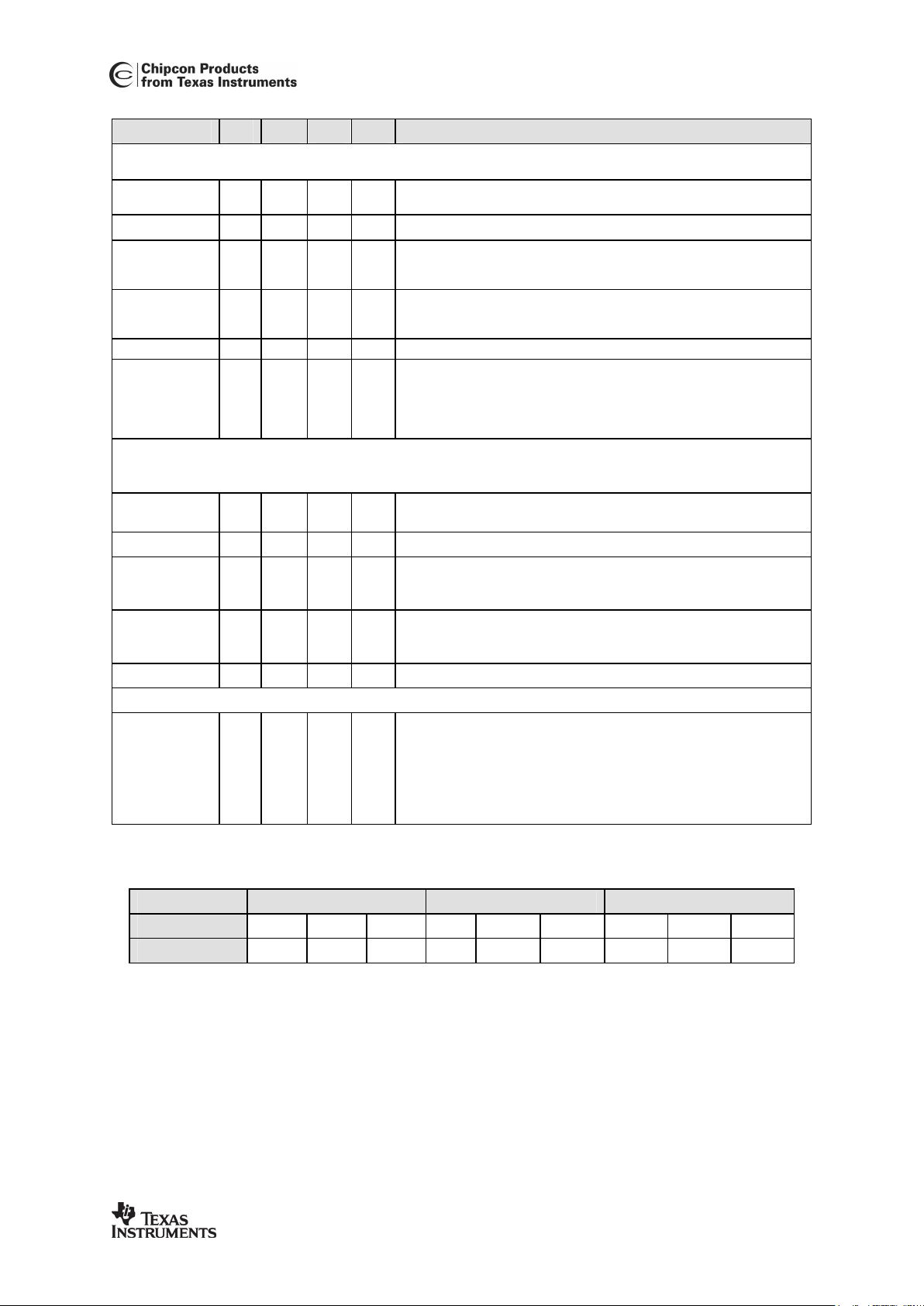
7.1 Current Consumption
T
A
= 25 °C, VDD = 3.0 V if nothing else stated. All measurement results are obtained using the
CC2510EM reference design ([1]).
Parameter Min Typ Max Unit Condition
4.8 mA System clock running at 26 MHz.
4.6 mA System clock running at 24 MHz.
Active mode, full
speed (high speed
crystal oscillator)
1
.
Low CPU activity.
Digital regulator on. High speed crystal oscillator and low power
RCOSC running. No peripherals running.
Low CPU activity: No flash access (i.e. only cache hit), no RAM
access
Active mode, full
speed (HS
RCOSC)
1
.
Low CPU activity.
2.5 mA System clock running at 26 MHz.
Digital regulator on. HS RCOSC and low power RCOSC running.
System clock running at 13 MHz. No peripherals running.
Low CPU activity: No flash access (i.e. only cache hit), no RAM
access
Digital regulator on. High speed crystal oscillator and low power
RCOSC running. Radio in RX mode (sensitivity optimized
MDMCFG2.DEM_DCFILT_OFF=0)
19.8 mA 2.4 kBaud, input at sensitivity limit, system clock running at 26 MHz.
17.1 mA 2.4 kBaud, input at sensitivity limit, system clock running at 203 kHz.
19.8 mA 2.4 kBaud, input well above sensitivity limit, system clock running at
26 MHz.
21.5 mA 10 kBaud, input at sensitivity limit, system clock running at 26 MHz.
18.8 mA 10 kBaud, input at sensitivity limit, system clock running at 203 kHz.
19.0 mA 10 kBaud, input well above sensitivity limit, system clock running at
26 MHz.
22.9 mA 250 kBaud, input at sensitivity limit, system clock running at 26 MHz.
20.5 mA 250 kBaud, input at sensitivity limit, system clock running at 1.625
MHz.
19.6 mA 250 kBaud, input well above sensitivity limit, system clock running at
26 MHz. See Figure 2 for typical variation over operating conditions
19.7 mA 500 kBaud, input at sensitivity limit, system clock running at 26 MHz.
17.5 mA 500 kBaud, input at sensitivity limit, system clock running at 3.25
MHz.
16.7 mA 500 kBaud, input well above sensitivity limit
Digital regulator on. High speed crystal oscillator and low power
RCOSC running. Radio in RX mode (current optimized
MDMCFG2.DEM_DCFILT_OFF=1)
17.4 mA 2.4 kBaud, input at sensitivity limit, system clock running at 26 MHz.
14.7 mA 2.4 kBaud, input at sensitivity limit, system clock running at 203 kHz.
17.4 mA 2.4 kBaud, input well above sensitivity limit, system clock running at
26 MHz.
19.4 mA 10 kBaud, input at sensitivity limit, system clock running at 26 MHz.
15.7 mA 10 kBaud, input at sensitivity limit, system clock running at 203 kHz.
Active mode with
radio in RX
16.9 mA 10 kBaud, input well above sensitivity limit, system clock running at
26 MHz.
1
Note: In order to reduce the current consumption in active mode, the clock speed can be reduced by
setting CLKCON.CLKSPD ≠ 000 (see section 13.1 for details). Figure 1 shows typical current
consumption in active mode for different clock speeds
C2510Fx / CC2511Fx
SWRS055D Page 11 of 243
Parameter Min Typ Max Unit Condition
System clock running at 24 MHz.
Digital regulator on. High speed crystal oscillator and low power
RCOSC running. Radio in RX mode (sensitivity optimized
MDMCFG2.DEM_DCFILT_OFF=0)
20.6 mA 2.4 kBaud, input at sensitivity limit
22.1 mA 10 kBaud, input at sensitivity limit
22.7 mA 250 kBaud, input at sensitivity limit
Active mode with
radio in RX
20.8 mA 500 kBaud, input at sensitivity limit
System clock running at 26 MHz.
Digital regulator on. High speed crystal oscillator and low power
RCOSC running. Radio in TX mode
26 mA
0 dBm output power (PA_TABLE0=0xFE). See Table 7 for typical
variation over operating conditions
18.5 mA
-6 dBm output power (PA_TABLE0=0x7F)
15.5 mA
-12 dBm output power (PA_TABLE0=0x95)
Active mode with
radio in TX
26 mA System clock running at 24 MHz.
Digital regulator on. High speed crystal oscillator and low power
RCOSC running. Radio in TX mode
w
/0 dBm output power
(PA_TABLE0=0xFE)
PM0 4.3 mA Same as active mode, but the CPU is not running (see 13.1.2.2 for
details). System clock running at 26 MHz
PM1 220
µA
Digital regulator on. HS RCOSC and high speed crystal oscillator off.
32.768 kHz XOSC or low power RCOSC running (see 13.1.2.3 for
details)
PM2 0.5 1
µA
Digital regulator off. HS RCOSC and high speed crystal oscillator off.
Low power RCOSC running (see 13.1.2.4 for details)
PM3 0.3 1
µA
Digital regulator off. No crystal oscillators or RC oscillators are
running (see 13.1.2.5 for details)
Peripheral
Current
Consumption
Add to the figures above if the peripheral unit is activated
Timer 1 2.7
µA/MHz
When running
Timer 2 1.3
µA/MHz
When running
Timer 3 1.6
µA/MHz
When running
Timer 4 2
µA/MHz
When running
ADC 1.2 mA During conversion
Table 6: Current Consumption
C2510Fx / CC2511Fx
SWRS055D Page 12 of 243
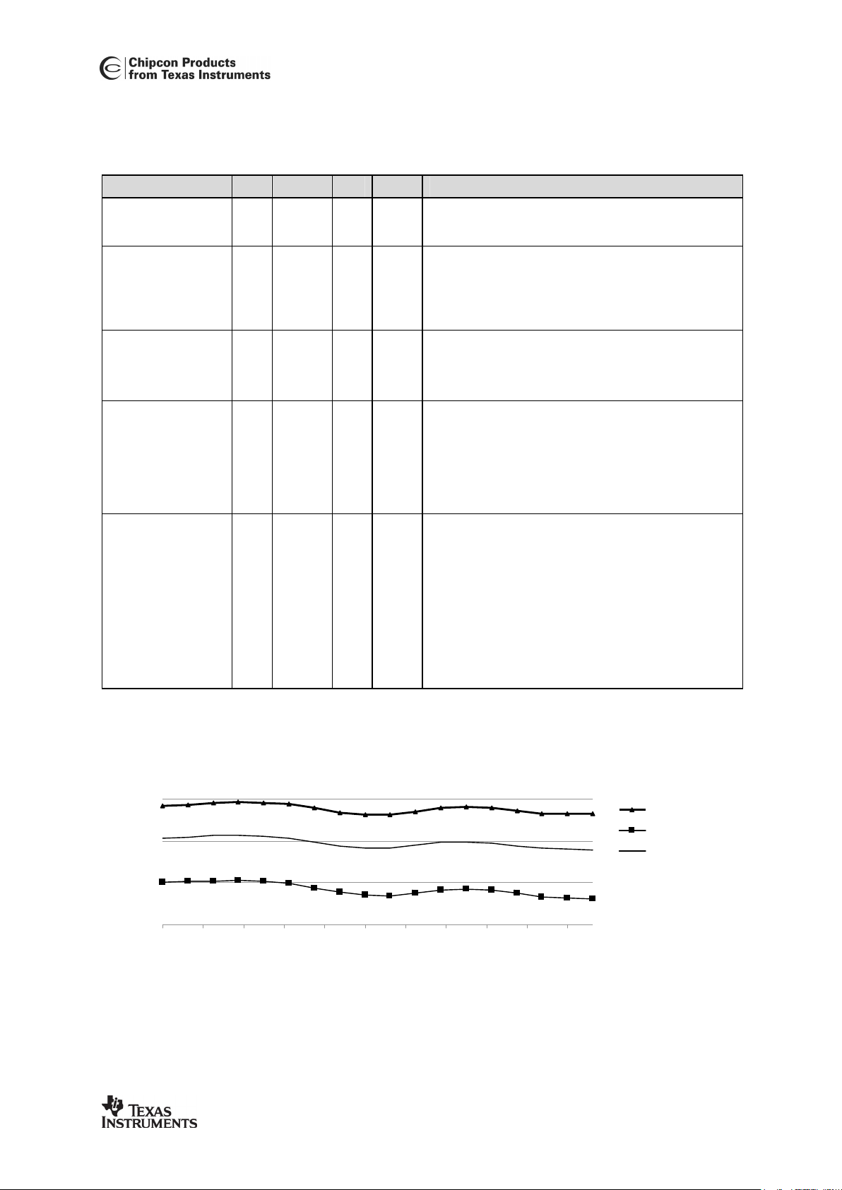
Figure 1: Current Consumption (Active Mode) vs. Clock Speed
Figure 2:
Typical Variation in RX Current Consumption over Temperature and Input Power Level.
Data Rate = 250 kBaud.
Supply Voltage, VDD = 2 V Supply Voltage, VDD = 3 V Supply Voltage, VDD = 3.6 V
Temperature [°C] -40 +25 +85 -40 +25 +85 -40 +25 +85
Current [mA] 26 25.6 26 26.3 26 26.3 26.5 26.2 26.6
Table 7: Typical Variation in TX Current Consumption over Temperature and Supply Voltage
Typical Variation in RX Current Consumption over
Temperature and Input Power Level.
Data Rate = 250 kBaud
15.0
17.0
19.0
21.0
23.0
25.0
-120 -100 -80 -60 -40 -20 0
Input Power Level [dBm]
Current [mA]
-40 °C
+25 °C
+85 °C
Current Consumption Active Mode. No Peripherals Running.
f
xosc
= 26 MHz
0,0
1,0
2,0
3,0
4,0
5,0
6,0
0 2 4 6 8 10121416182022242628
Clock Speed [MHz]
Measurements done for all valid CLKCON.CLKSPD settings
(000 – 111 for HS XOSC, 001 – 111 for HS RCOSC)
Current [mA]
HS XOSC
HS RCOSC
C2510Fx / CC2511Fx
SWRS055D Page 13 of 243
7.2 RF Receive Section
T
A
= 25 °C, VDD = 3.0 V if nothing else stated. All measurement results are obtained using the
CC2510EM reference design ([1]).
Parameter Min Typ Max Unit Condition/Note
Digital channel
filter bandwidth
58 812 kHz User programmable (see Section 14.6). The bandwidth limits are
proportional to crystal frequency (given values assume a 26.0 MHz
crystal).
2.4 kBaud data rate, sensitivity optimized, MDMCFG2.DEM_DCFILT_OFF=0
(2-FSK, 1% packet error rate, 20 bytes packet length, 203 kHz digital channel filter bandwidth)
Receiver
sensitivity
-103
dBm
The RX current consumption can be reduced by approximately 2.4 mA
by setting MDMCFG2.DEM_DCFILT_OFF=1. The typical sensitivity is then
-101 dBm.
The sensitivity can be improved to typically -105 dBm with
MDMCFG2.DEM_DCFILT_OFF=0
by changing registers TEST2 and
TEST1 (see Page 227). The temperature range is then from 0
o
C to +85
o
C.
Saturation -10 dBm
Adjacent
channel
rejection
23 dB Desired channel 3 dB above the sensitivity limit. 250 kHz channel
spacing
Alternate
channel
rejection
32 dB Desired channel 3 dB above the sensitivity limit. 250 kHz channel
spacing
See Figure 54 for plot of selectivity versus frequency offset
Blocking
±10 MHz offset
±20 MHz offset
±50 MHz offset
64
70
71
dB
dB
dB
Wanted signal 3 dB above sensitivity level.
Compliant with ETSI EN 300 440 class 2 receiver requirements.
10 kBaud data rate, sensitivity optimized, MDMCFG2.DEM_DCFILT_OFF=0
(2-FSK, 1% packet error rate, 20 bytes packet length, 232 kHz digital channel filter bandwidth)
Receiver
sensitivity
-98 dBm The RX current consumption can be reduced by approximately 2.2 mA
by setting MDMCFG2.DEM_DCFILT_OFF=1. The typical sensitivity is then
-97 dBm.
The sensitivity can be improved to typically -100 dBm with
MDMCFG2.DEM_DCFILT_OFF=0
by changing registers TEST2 and
TEST1 (see Page 227). The temperature range is then from 0
o
C to +85
o
C.
Saturation -9 dBm
Adjacent
channel
rejection
19 dB Desired channel 3 dB above the sensitivity limit. 250 kHz channel
spacing
Alternate
channel
rejection
25 dB Desired channel 3 dB above the sensitivity limit. 250 kHz channel
spacing
See Figure 55 for plot of selectivity versus frequency offset
Blocking
±10 MHz offset
±20 MHz offset
±50 MHz offset
59
65
66
dB
dB
dB
Wanted signal 3 dB above sensitivity level.
Compliant with ETSI EN 300 440 class 2 receiver requirements.
C2510Fx / CC2511Fx
SWRS055D Page 14 of 243
Parameter Min Typ Max Unit Condition/Note
250 kBaud data rate, sensitivity optimized, MDMCFG2.DEM_DCFILT_OFF=0
(MSK, 1% packet error rate, 20 bytes packet length, 540 kHz digital channel filter bandwidth)
Receiver
sensitivity
-90 dBm See Table 9 for typical variation over operating conditions
Saturation -11 dBm
Adjacent
channel
rejection
21 dB Desired channel 3 dB above the sensitivity limit. 750 kHz channel
spacing
Alternate
channel
rejection
30 dB Desired channel 3 dB above the sensitivity limit. 750 kHz channel
spacing
See Figure 56 for plot of selectivity versus frequency offset
Blocking
±10 MHz offset
±20 MHz offset
±50 MHz offset
46
53
55
dB
dB
dB
Wanted signal 3 dB above sensitivity level.
Compliant with ETSI EN 300 440 class 2 receiver requirements.
500 kBaud data rate, sensitivity optimized, MDMCFG2.DEM_DCFILT_OFF=0 (MDMCFG2.DEM_DCFILT_OFF=1 cannot
be used for data rates >100 kBaud)
(MSK, 1% packet error rate, 20 bytes packet length, 812 kHz digital channel filter bandwidth)
Receiver
sensitivity
-82 dBm
Saturation -15 dBm
Adjacent
channel
rejection
12 dB Desired channel 3 dB above the sensitivity limit. 1 MHz channel spacing
Alternate
channel
rejection
23 dB Desired channel 3 dB above the sensitivity limit. 1 MHz channel spacing
See Figure 58 for plot of selectivity versus frequency offset
General
Spurious
emissions
Conducted measurement in a 50 Ω single ended load. Complies with EN
300 328, EN 300 440 class 2, FCC CFR47, Part 15 and ARIB STD-T-66.
25 MHz –
1 GHz
-57 dBm
Above 1 GHz
-47 dBm
Table 8: RF Receive Section
Supply Voltage, VDD = 2 V Supply Voltage, VDD = 3 V Supply Voltage, VDD = 3.6 V
Temperature [°C] -40 +25 +85 -40 +25 +85 -40 +25 +85
Sensitivity [dBm] -91.5 -90.3 -88.7 -90 -89.6 -88.1 -88.7 -89.3 -88.4
Table 9: Typical Variation in Sensitivity over Temperature and Supply Voltage @ 2.44 GHz and
250 kBaud Data Rate
C2510Fx / CC2511Fx
SWRS055D Page 15 of 243
7.3 RF Transmit Section
T
A
= 25 °C, VDD = 3.0 V if nothing else stated. All measurement results are obtained using the
CC2510EM reference designs ([1]).
Parameter Min Typ Max Unit Condition/Note
Differential load
impedance
80 + j74
Ω
Differential impedance as seen from the RF-port (RF_P and
RF_N) towards the antenna. Follow the CC2510EM
reference design [1] available from TI’s website.
Output power, highest
setting
+1 dBm Output power is programmable and is available across the
entire frequency band. See Figure 3 typical variation over
operating conditions (output power is 0 dBm)
Delivered to a 50 Ω single-ended load via the CC2510EM
reference design [1] RF matching network.
Output power, lowest
setting
-30 dBm Output power is programmable and is available across the
entire frequency band
Delivered to a 50 Ω single-ended load via the CC2510EM
reference design [1] RF matching network.
Occupied bandwidth
(99%)
-28
-27
-22
-21
dBc
dBc
dBc
dBc
2.4 kBaud, 38.2 kHz deviation, 2-FSK, 250 kHz channel
spacing
10 kBaud, 38.2 kHz deviation, 2-FSK, 250 kHz channel
spacing
250 kBaud, MSK, 750 kHz channel spacing
500 kBaud, MSK, 1 MHz channel spacing
Spurious emissions 0 dBm output power.
25 MHz – 1 GHz -36 dBm
47 - 74, 87.5 - 118,
174 - 230, and 470 862 MHz
-54 dBm
1800-1900 MHz -47 dBm Restricted band in Europe
At 2·RF and 3·RF -41 dBm Restricted bands in USA
Otherwise above
1 GHz
-30 dBm
Table 10: RF Transmit Section
Figure 3: Typical Variation in Output Power over Frequency and Temperature
(0 dBm output power)
Typical Variation in Output Power (0 dBm) over Frequency and
Temperature
2
2400 2408 2416 2424 2432 2440 2448 2456 2464 2472 2480
Frequency [MHz]
Output Power [dBm]
A
vg -40 °C
A
vg +85 °C
A
vg +25 °C
0
-2
-2

C2510Fx / CC2511Fx
SWRS055D Page 16 of 243
7.4 Crystal Oscillators
7.4.1
CC2510Fx
Crystal Oscillator
T
A
= 25 °C, VDD = 3.0 V if nothing else is stated.
Parameter Min Typ Max Unit Condition/Note
Crystal frequency 24 26 27 MHz Referred to as f
XOSC.
For operation in the range 24 – 26 MHz, please
refer to Table 4 for Operating Conditions.
Crystal frequency
accuracy
requirement
±40 ppm This is the total tolerance including a) initial tolerance, b) crystal
loading, c) aging, and d) temperature dependence.
The acceptable crystal tolerance depends on RF frequency and
channel spacing / bandwidth.
C0 1 5 7 pF Simulated over operating conditions
Load capacitance 10 13 20 pF Simulated over operating conditions
ESR 100
Ω
Simulated over operating conditions
Start-up time 250 µs f
XOSC
= 26 MHz
Note: A Ripple counter of 12 bit is included to ensure duty-cycle
requirements. Start-up time includes ripple counter delay until
SLEEP.XOSC_STB is asserted
Table 11:
CC2510Fx
Crystal Oscillator Parameters
7.4.2
CC2511Fx
Crystal Oscillator
T
A
= 25 °C, VDD = 3.0 V if nothing else is stated.
Parameter Min Typ Max Unit Condition/Note
Crystal frequency 48 MHz Referred to as f
XOSC
Crystal frequency
accuracy
requirement
±40 ppm This is the total tolerance including a) initial tolerance, b) crystal
loading, c) aging, and d) temperature dependence.
The acceptable crystal tolerance depends on RF frequency and
channel spacing / bandwidth.
C0
Fundamental 0.85 1 1.15 pF Simulated over operating conditions. Variation given by reference
crystal NX2520SA from NDK
3rd overtone 2 3 7 pF
Load capacitance 15 16 17 pF Simulated over operating conditions
ESR 60
Ω
Simulated over operating conditions
Start-up time
Note: A Ripple counter of 14 bit is included to ensure duty-cycle
requirements. Start-up time includes ripple counter delay until
SLEEP.XOSC_STB is asserted
Fundamental 650 µs
3rd overtone 3 ms Simulated value
Table 12:
CC2511Fx
Crystal Oscillator Parameters
C2510Fx / CC2511Fx
SWRS055D Page 17 of 243
7.5 32.768 kHz Crystal Oscillator
T
A
= 25 °C, VDD = 3.0V if nothing else is stated.
Parameter Min Typ Max Unit Condition/Note
Crystal frequency 32.768 kHz
C0 0.9 2.0 pF Simulated over operating conditions
Load capacitance 12 16 pF Simulated over operating conditions
ESR 40 130
kΩ
Simulated over operating conditions
Start-up time 400 ms Value is simulated
Table 13: 32.768 kHz Crystal Oscillator Parameters
C2510Fx / CC2511Fx
SWRS055D Page 18 of 243
7.6 Low Power RC Oscillator
T
A
= 25 °C, VDD = 3.0 V if nothing else is stated.
Parameter Min Typ Max Unit Condition/Note
Calibrated frequency2 32.0 34.7 36.0 kHz Calibrated low power RC oscillator frequency is
f
XOSC
/ 750
Frequency accuracy after
calibration
±1 %
Temperature coefficient +0.5
%/°C
Frequency drift when temperature changes after
calibration
Supply voltage coefficient +3 %/V Frequency drift when supply voltage changes after
calibration
Initial calibration time 2 ms When the low power RC oscillator is enabled,
calibration is continuously done in the background
as long as the high speed crystal oscillator is
running.
Table 14: Low Power RC Oscillator Parameters
7.7 High Speed RC Oscillator
T
A
= 25 °C, VDD = 3.0 V if nothing else is stated.
Parameter Min Typ Max Unit Condition/Note
Calibrated frequency2 12 13 13.5 MHz Calibrated HS RCOSC frequency is f
XOSC
/ 2
Uncalibrated frequency
accuracy
±15
%
Calibrated frequency
accuracy
±1
%
Start-up time 10 µs
Temperature coefficient -325
ppm/°C
Frequency drift when temperature changes after
calibration
Supply voltage coefficient 28 ppm/V Frequency drift when supply voltage changes after
calibration
Initial calibration time 65 µs The HS RCOSC will be calibrated once when the
high speed crystal oscillator is selected as system
clock source (CLKCON.OSC is set to 0), and also
when the system wakes up from PM{1-3}. See
13.1.5.1 for details).
Table 15: High Speed RC Oscillator Parameters
2
Min figures are given using f
XOSC
= 24 MHz. Typ figures are given using f
XOSC
= 26 MHz, and Max
figures are given using f
XOSC
= 27 MHz
C2510Fx / CC2511Fx
SWRS055D Page 19 of 243
7.8 Frequency Synthesizer Characteristics
T
A
= 25 °C, VDD = 3.0 V if nothing else stated. All measurement results are obtained using the
CC2510EM reference designs ([1]).
Parameter Min Typ Max Unit Condition/Note
Programmed frequency
resolution
367 397 412 Hz 24 - 27 MHz crystal.
Frequency resolution = f
XOSC
/ 216
Synthesizer frequency
tolerance
±40 ppm Given by crystal used. Required accuracy (including
temperature and aging) depends on frequency band and
channel bandwidth / spacing.
RF carrier phase noise -77 dBc/Hz @ 50 kHz offset from carrier
RF carrier phase noise -77 dBc/Hz @ 100 kHz offset from carrier
RF carrier phase noise -78 dBc/Hz @ 200 kHz offset from carrier
RF carrier phase noise -88 dBc/Hz @ 500 kHz offset from carrier
RF carrier phase noise -98 dBc/Hz @ 1 MHz offset from carrier
RF carrier phase noise -107 dBc/Hz @ 2 MHz offset from carrier
RF carrier phase noise -116 dBc/Hz @ 5 MHz offset from carrier
RF carrier phase noise -125 dBc/Hz @ 10 MHz offset from carrier
PLL turn-on / hop time3 85.1 88.4 95.8
µs
Time from leaving the IDLE state until arriving in the RX,
FSTXON, or TX state, when not performing calibration.
Crystal oscillator running.
PLL RX/TX settling time3 9.3 9.6 10.4
µs
Settling time for the 1·IF frequency step from RX to TX
PLL TX/RX settling time3 20.7 21.5 23.3
µs
Settling time for the 1·IF frequency step from TX to RX
PLL calibration time3 694 721 780.8
µs
Calibration can be initiated manually or automatically
before entering or after leaving RX/TX.
Table 16: Frequency Synthesizer Parameters
7.9 Analog Temperature Sensor
T
A
= 25 °C, VDD = 3.0V if nothing else stated. All measurement results are obtained using the
CC2510EM reference designs ([1]).
Parameter Min Typ Max Unit Condition/Note
Output voltage at -40 °C
0.654 V
Output voltage at 0 °C
0.750 V
Output voltage at +40 °C
0.848 V
Output voltage at +80 °C
0.946 V
Temperature coefficient 2.43
mV/°C Fitted from -20 °C to +80 °C
Error in calculated
temperature, calibrated
-2
*
0 2
*
°C From -20°C to +80°C when using 2.43 mV / °C, after 1-point
calibration at room temperature
*
The indicated minimum and maximum error with 1-point
calibration is based on measured values for typical process
parameters
Current consumption
increase when enabled
0.3 mA
Table 17: Analog Temperature Sensor Parameters
3
Min figures are given using f
XOSC
= 27 MHz. Typ figures are given using f
XOSC
= 26 MHz, and Max
figures are given using f
XOSC
= 24 MHz.
C2510Fx / CC2511Fx
SWRS055D Page 20 of 243
7.10 7-12 bit ADC
T
A
= 25 °C, VDD = 3.0V if nothing else stated. The numbers given here are based on tests performed
in accordance with IEEE Std 1241-2000 [7]. The ADC data are from
CC2430
characterization. As the
CC2510x/C2511Fx
uses the same ADC, the numbers listed in Table 18 should be good indicators of the
performance to be expected from
CC2510x
and
CC2511x
. Note that these numbers will apply for 24 MHz
operated systems (like
CC2510x
using a 24 MHz crystal or
CC2511x
using a 48 MHz crystal).
Performance will be slightly different for other crystal frequencies (e.g. 26 MHz and 27 MHz).
Parameter Min Typ Max Unit Condition/Note
Input voltage 0 AVDD V AVDD is voltage on AVDD pin
External reference voltage 0 AVDD V AVDD is voltage on AVDD pin
External reference voltage
differential
0 AVDD V AVDD is voltage on AVDD pin
Input resistance, signal 197
kΩ
Simulated using 4 MHz clock speed (see Section
13.10.2.7)
Full-Scale Signal4 2.97 V Peak-to-peak, defines 0 dBFS
ENOB4 5.7 bits 7-bits setting
Single ended input 7.5 9-bits setting
9.3 10-bits setting
10.8 12-bits setting
ENOB4 6.5 bits 7-bits setting
Differential input 8.3 9-bits setting
10.0 10-bits setting
11.5 12-bits setting
Useful Power Bandwidth 0-20 kHz 7-bits setting, both single and differential
THD4
-Single ended input -75.2 dB 12-bits setting, -6 dBFS
-Differential input -86.6 dB 12-bits setting, -6 dBFS
Signal To Non-Harmonic Ratio4
-Single ended input 70.2 dB 12-bits setting
-Differential input 79.3 dB 12-bits setting
Spurious Free Dynamic Range4
-Single ended input 78.8 dB 12-bits setting, -6 dBFS
-Differential input 88.9 dB 12-bits setting, -6 dBFS
CMRR, differential input <-84 dB 12- bit setting, 1 kHz Sine (0 dBFS), limited by ADC
resolution
Crosstalk, single ended input <-84 dB 12- bit setting, 1 kHz Sine (0 dBFS), limited by ADC
resolution
Offset -3 mV Mid. Scale
Gain error 0.68 %
DNL4 0.05 LSB 12-bits setting, mean
0.9 LSB 12-bits setting, max
INL4 4.6 LSB 12-bits setting, mean
13.3 LSB 12-bits setting, max
SINAD4 35.4 dB 7-bits setting
4
Measured with 300 Hz Sine input and VDD as reference.
C2510Fx / CC2511Fx
SWRS055D Page 21 of 243
Parameter Min Typ Max Unit Condition/Note
Single ended input 46.8 dB 9-bits setting
(-THD+N) 57.5 dB 10-bits setting
66.6 dB 12-bits setting
SINAD4 40.7 dB 7-bits setting
Differential input 51.6 dB 9-bits setting
(-THD+N) 61.8 dB 10-bits setting
70.8 dB 12-bits setting
Conversion time 20
µs
7-bits setting
36
µs
9-bits setting
68
µs
10-bits setting
132
µs
12-bits setting
Current consumption 1.2 mA
Table 18: 7-12 bit ADC Characteristics
7.11 Control AC Characteristics
T
A
= 25 °C, VDD = 3.0 V if nothing else stated. All measurement results are obtained using the
CC2510EM reference designs ([1]).
Parameter Min Typ Max Unit Condition/Note
System clock,
f
SYSCLK
t
SYSCLK
= 1/ f
SYSCLK
CC2510Fx
0.1875 26 27 MHz High speed crystal oscillator used as source (HS XOSC)
MHz Calibrated HS RCOSC used as source. 0.1875 13 13.5
HS
XOSC
HS
RCOSC
Min: f
XOSC
= 24 MHz, CLKCON.CLKSPD =
Typ: f
XOSC
= 26 MHz, CLKCON.CLKSPD =
Max: f
XOSC
= 27 MHz, CLKCON.CLKSPD =
111
000
000
111
001
001
0.1875 24
24
MHz
CC2511Fx
High speed crystal oscillator used as source.
0.1875 12 12 HS RCOSC used as source.
Min: f
XOSC
= 48 MHz, CLKCON.CLKSPD = 111
Typ and Max: f
XOSC
= 48 MHz, CLKCON.CLKSPD = 000
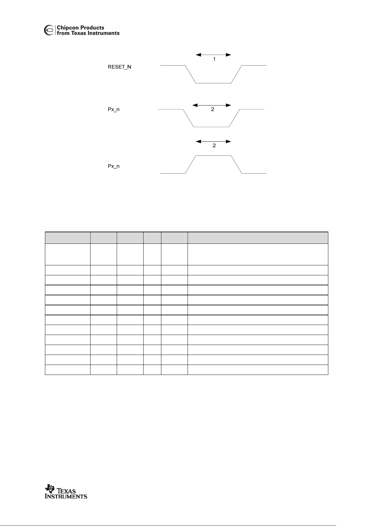
RESET_N low
width
250 ns See item 1, Figure 4. This is the shortest pulse that is
guaranteed to be recognized as a reset pin request.
Note: Shorter pulses may be recognized but will not lead to
complete reset of all modules within the chip.
Interrupt pulse
width
t
SYSCLK
See item 2, Figure 4. This is the shortest pulse that is
guaranteed to be recognized as an interrupt request. In PM2/3
the internal synchronizers are bypassed so this requirement
does not apply in PM2/3.
Table 19: Control Inputs AC Characteristics
C2510Fx / CC2511Fx
SWRS055D Page 22 of 243
Figure 4: Control Inputs AC Characteristics
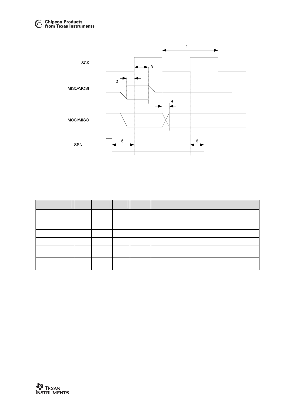
7.12 SPI AC Characteristics
T
A
= 25 °C, VDD = 3.0V if nothing else stated. All measurement results are obtained using the
CC2510EM reference designs ([1]).
Parameter Min Typ Max Unit Condition/Note
SCK period See
Section
13.14.3
ns Master. See item 1, Figure 5
SCK duty cycle 50 % Master.
SSN low to SCK 2·t
SYSCLK
See item 5, Figure 5
SCK to SSN high 30 ns See item 6, Figure 5
MISO setup 10 ns Master. See item 2, Figure 5
MISO hold 10 ns Master. See item 3, Figure 5
SCK to MOSI 25 ns Master. See item 4, Figure 5, load = 10 pF
SCK period 100 ns Slave. See item 1, Figure 5
SCK duty cycle 50 % Slave.
MOSI setup 10 ns Slave. See item 2, Figure 5
MOSI hold 10 ns Slave. See item 3, Figure 5
SCK to MISO 25 ns Slave. See item 4, Figure 5, load = 10 pF
Table 20: SPI AC Characteristics
C2510Fx / CC2511Fx
SWRS055D Page 23 of 243
Figure 5: SPI AC Characteristics
7.13 Debug Interface AC Characteristics
T
A
= 25 °C, VDD = 3.0 V if nothing else stated. All measurement results are obtained using the
CC2510EM reference designs ([1]).
Parameter Min Typ Max Unit Condition/Note
Debug clock
period
125 ns See item 1, Figure 6
Note: CLKCON.CLKSPD must be 000 or 001 when using
the debug interface
Debug data setup 5 ns See item 2, Figure 6
Debug data hold 5 ns See item 3, Figure 6
Clock to data
delay
10 ns See item 4, Figure 6, load = 10 pF
RESET_N inactive
after P2_2 rising
10 ns See item , Figure 6
Table 21: Debug Interface AC Characteristics
C2510Fx / CC2511Fx
SWRS055D Page 24 of 243
Figure 6: Debug Interface AC Characteristics
7.14 Port Outputs AC Characteristics
T
A
= 25 °C, VDD = 3.0 V if nothing else stated. All measurement results are obtained using the
CC2510EM reference designs ([1]).
Parameter Min Typ Max Unit Condition/Note
P0_[0:7], P1_[2:7],
P2_[0:4] Port output
rise time
(PICTL.PADSC=0 /
PICTL.PADSC=1)
3.15 /
1.34
ns Load = 10 pF
Timing is with respect to 10% VDD and 90% VDD levels.
Values are estimated
P0_[0:7], P1_[2:7],
P2_[0:4] Port output
fall time
(PICTL.PADSC=0 /
PICTL.PADSC=1)
3.2 / 1.44 ns Load = 10 pF
Timing is with respect to 90% VDD and 10% VDD.
Values are estimated
Table 22: Port Outputs AC Characteristics
7.15 Timer Inputs AC Characteristics
T
A
= 25 °C, VDD = 3.0 V if nothing else stated. All measurement results are obtained using the
CC2510EM reference designs ([1]).
Parameter Min Typ Max Unit Condition/Note
Input capture
pulse width
t
SYSCLK
Synchronizers determine the shortest input pulse that can be
recognized. The synchronizers operate from the current
system clock rate (see Table 19)
Table 23: Timer Inputs AC Characteristics
7.16 DC Characteristics
The DC Characteristics of
CC2510Fx/CC2511Fx
are listed in Table 24 below.
T
A
= 25 °C, VDD = 3.0 V if nothing else stated. All measurement results are obtained using the
CC2510EM reference designs ([1]).
Digital Inputs/Outputs Min Typ Max Unit Condition

C2510Fx / CC2511Fx
SWRS055D Page 25 of 243
Logic "0" input voltage 30 % Of VDD supply (2.0 – 3.6 V)
Logic "1" input voltage 70 % Of VDD supply (2.0 – 3.6 V)
Logic "0" input current per pin NA 12 nA Input equals 0 V
Logic "1" input current per pin NA 12 nA Input equals VDD
Total logic “0” input current all pins 70 nA
Total logic “1” input current all pins 70 nA
I/O pin pull-up and pull-down resistor 20
kΩ
Table 24: DC Characteristics
C2510Fx / CC2511Fx
SWRS055D Page 26 of 243
8 Pin and I/O Port Configuration
The
CC2510Fx
pin-out is shown in Figure 7 and Table 25. See Section 13.4 for details on the I/O
configuration.
AGND
Exposed die
attached pad
DVDD
36 35 34 33 32 31 30 29 28
9
8
7
6
5
4
3
2
1
27
26
25
24
23
22
21
20
19
10 11 12 13 14 15 16 17 18
P1_1
P1_0
P0_0
P0_1
P0_2
P0_3
P0_4
AVDD
XOSC_Q2
AVDD
RF_N
AVDD
AVDD
RBIAS
XOSC_Q1
RF_P
P1_2
Figure 7:
CC2510Fx
Pinout Top View
Note: The exposed die attach pad must be connected to a solid ground plane as this is the ground
connection for the chip.
C2510Fx / CC2511Fx
SWRS055D Page 27 of 243
Pin Pin Name Pin Type Description
AGND Ground The exposed die attach pad must be connected to a solid ground
plane
1 P1_2 D I/O Port 1.2
2 DVDD Power (Digital) 2.0 V - 3.6 V digital power supply for digital I/O
3 P1_1 D I/O Port 1.1
4 P1_0 D I/O Port 1.0
5 P0_0 D I/O Port 0.0
6 P0_1 D I/O Port 0.1
7 P0_2 D I/O Port 0.2
8 P0_3 D I/O Port 0.3
9 P0_4 D I/O Port 0.4
10 DVDD Power (Digital) 2.0 V - 3.6 V digital power supply for digital I/O
11 P0_5 D I/O Port 0.5
12 P0_6 D I/O Port 0.6
13 P0_7 D I/O Port 0.7
14 P2_0 D I/O Port 2.0
15 P2_1 D I/O Port 2.1
16 P2_2 D I/O Port 2.2
17 P2_3/XOSC32_Q1 D I/O Port 2.3/32.768 kHz crystal oscillator pin 1
18 P2_4/XOSC32_Q2 D I/O Port 2.4/32.768 kHz crystal oscillator pin 2
19 AVDD Power (Analog) 2.0 V - 3.6 V analog power supply connection
20 XOSC_Q2 Analog I/O 26 MHz crystal oscillator pin 2
21 XOSC_Q1 Analog I/O 26 MHz crystal oscillator pin 1, or external clock input
22 AVDD Power (Analog) 2.0 V - 3.6 V analog power supply connection
23 RF_P RF I/O Positive RF input signal to LNA in receive mode
Positive RF output signal from PA in transmit mode
24 RF_N RF I/O Negative RF input signal to LNA in receive mode
Negative RF output signal from PA in transmit mode
25 AVDD Power (Analog) 2.0 V – 3.6 V analog power supply connection
26 AVDD Power (Analog) 2.0 V - 3.6 V analog power supply connection
27 RBIAS Analog I/O External precision bias resistor for reference current
28 GUARD Power (Digital) Power supply connection for digital noise isolation
29 AVDD_DREG Power (Digital) 2.0 V - 3.6 V digital power supply for digital core voltage regulator
30 DCOUPL Power decoupling 1.8 V digital power supply decoupling
31 RESET_N DI Reset, active low
32 P1_7 D I/O Port 1.7
33 P1_6 D I/O Port 1.6
34 P1_5 D I/O Port 1.5
35 P1_4 D I/O Port 1.4
36 P1_3 D I/O Port 1.3
Table 25:
CC2510Fx
Pin-out Overview

C2510Fx / CC2511Fx
SWRS055D Page 28 of 243
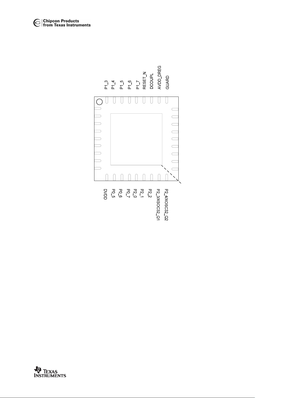
The
CC2511Fx
pin-out is shown in Figure 8 and Table 26. See Section 13.4 for details on the I/O
configuration.
AGND
Exposed die
attached pad
DVDD
36 35 34 33 32 31 30 29 28
9
8
7
6
5
4
3
2
1
27
26
25
24
23
22
21
20
19
10 11 12 13 14 15 16 17 18
P1_1
P1_0
P0_0
P0_1
P0_2
P0_3
P0_4
AVDD
XOSC_Q2
AVDD
RF_N
AVDD
AVDD
R_BIAS
XOSC_Q1
RF_P
P1_2
Figure 8:
CC2511Fx
Pin-out Top View
Note: The exposed die attach pad must be connected to a solid ground plane as this is the ground
connection for the chip.
C2510Fx / CC2511Fx
SWRS055D Page 29 of 243
Pin Pin Name Pin Type Description
AGND Ground The exposed die attach pad must be connected to a solid ground
plane
1 P1_2 D I/O Port 1.2
2 DVDD Power (Digital) 2.0 V - 3.6 V digital power supply for digital I/O
3 P1_1 D I/O Port 1.1
4 P1_0 D I/O Port 1.0
5 P0_0 D I/O Port 0.0
6 P0_1 D I/O Port 0.1
7 P0_2 D I/O Port 0.2
8 P0_3 D I/O Port 0.3
9 P0_4 D I/O Port 0.4
10 DP USB I/O USB Differential Data Bus Plus
11 DM USB I/O USB Differential Data Bus Minus
12 DVDD Power (Digital) 2.0 V - 3.6 V digital power supply for digital I/O
13 P0_5 D I/O Port 0.5
14 P2_0 D I/O Port 2.0
15 P2_1 D I/O Port 2.1
16 P2_2 D I/O Port 2.2
17 P2_3/XOSC32_Q1 D I/O Port 2.3/32.768 kHz crystal oscillator pin 1
18 P2_4/XOSC32_Q2 D I/O Port 2.4/32.768 kHz crystal oscillator pin 2
19 AVDD Power (Analog) 2.0 V - 3.6 V analog power supply connection
20 XOSC_Q2 Analog I/O 48 MHz crystal oscillator pin 2
21 XOSC_Q1 Analog I/O 48 MHz crystal oscillator pin 1, or external clock input
22 AVDD Power (Analog) 2.0 V - 3.6 V analog power supply connection
23 RF_P RF I/O Positive RF input signal to LNA in receive mode
Positive RF output signal from PA in transmit mode
24 RF_N RF I/O Negative RF input signal to LNA in receive mode
Negative RF output signal from PA in transmit mode
25 AVDD Power (Analog) 2.0 V - 3.6 V analog power supply connection
26 AVDD Power (Analog) 2.0 V - 3.6 V analog power supply connection
27 RBIAS Analog I/O External precision bias resistor for reference current
28 GUARD Power (Digital) Power supply connection for digital noise isolation
29 AVDD_DREG Power (Digital) 2.0 V - 3.6 V digital power supply for digital core voltage regulator
30 DCOUPL Power
decoupling
1.8 V digital power supply decoupling
31 RESET_N DI Reset, active low
32 P1_7 D I/O Port 1.7
33 P1_6 D I/O Port 1.6
34 P1_5 D I/O Port 1.5
35 P1_4 D I/O Port 1.4
36 P1_3 D I/O Port 1.3
Table 26:
CC2511Fx
Pin-out Overview
C2510Fx / CC2511Fx
SWRS055D Page 30 of 243
9 Circuit Description
SFR bus SFR bus
MEMORY
ARBITRATOR
8051 CPU
CORE
DMA
32 KB
FLASH
4 KB
SRAM
FLASH CTRL
DEBUG
INTERFACE
RESET
RESET_N
P2_4
P2_3
P2_2
P2_1
P2_0
P1_4
P1_3
P1_2
P1_1
P1_0
P1_7
P1_6
P1_5
P0_4
P0_3
P0_2
P0_1
P0_0
P0_5
32.768 kHz
CRYSTAL OSC
HIGH SPEED
CRYSTAL OSC
(24 – 27 MHz)
HIGH SPEED
RC-OSC
LOW PWR
RC-OSC
CLOCK MUX &
CALIBRATION
RAM
I/O CONTROLLER
USART 0
USART 1
TIMER 1 (16-bit) + Module
TIMER 3 (8-bit)
TIMER 2 (8-bit MAC Timer)
TIMER 4 (8-bit)
AES
ENCRYPTION &
DECRYPTION
WATCHDOG TIMER
RADIO DATA INTERFACE
IRQ
CTRL
FLASH
UNIFIED
FRAME CONTROL
AGC
RF_P RF_N
SYNTH
MODULATORDEMODULATOR
POWER ON RESET
RADIO / I2S REGISTERS
POWER MGT. CONTROLLER
SLEEP TIMER
CODE
XDATA
DATA
SFR
XOSC_Q2
XOSC_Q1
RECEIVE
CHAIN
TRANSMIT
CHAIN
ADC
AUDIO / DC
DIGITAL
ANALOG
MIXED
VDD (2.0 - 3.6 V)
DCOUPL
ON-CHIP VOLTAGE
REGULATOR
FREQUENCY
SYNTHESIZER
USB
USB BUS
USB PHY
DM
DP
1 KB
FIFO SRAM
P0_7
P0_6
I2S
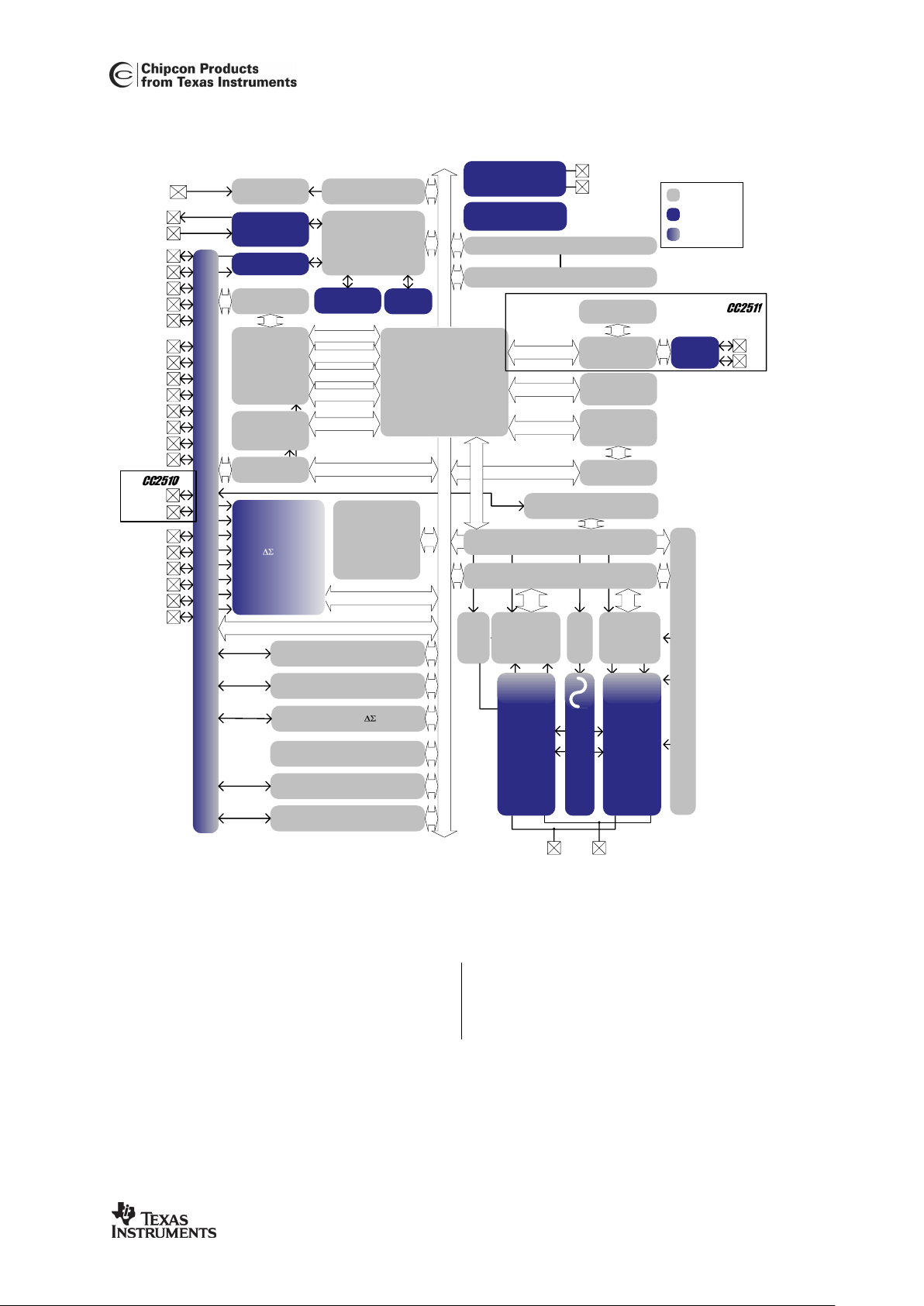
Figure 9:
C C2510Fx/CC2511Fx
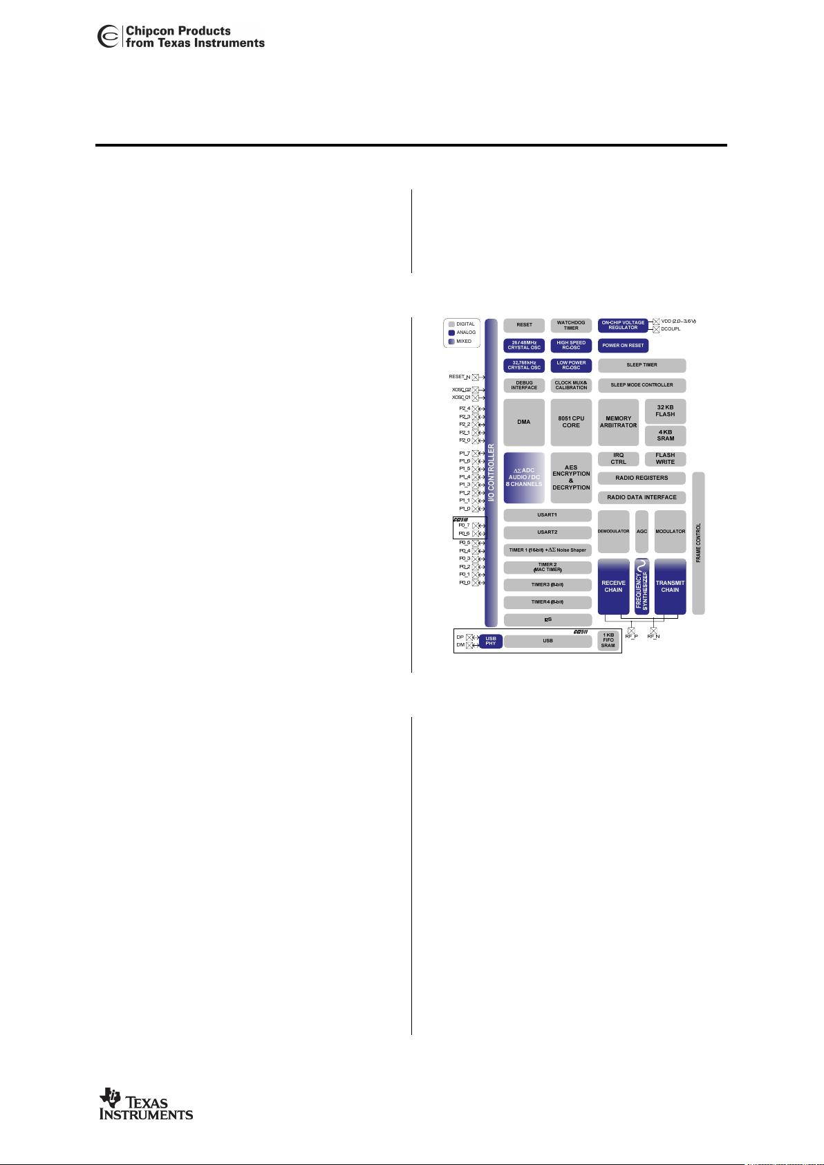
Block Diagram
A block diagram of
CC2510Fx/CC2511Fx
is
shown in Figure 9. The modules can be
divided into one out of three categories: CPUrelated modules, radio-related modules, and
modules related to power, test, and clock
distribution. In the following subsections, a
short description of each module that appears
in Figure 9.

C2510Fx / CC2511Fx
SWRS055D Page 31 of 243
9.1 CPU and Peripherals
The 8051 CPU core is a single-cycle 8051compatible core. It has three different memory
access buses (SFR, DATA and
CODE/XDATA), a debug interface, and an
extended interrupt unit servicing 18 interrupt
sources. See Section 9.1 for details on the
CPU.
The memory crossbar/arbitrator is at the
heart of the system as it connects the CPU
and DMA controller with the physical
memories and all peripherals through the SFR
bus. The memory arbitrator has four memory
access points, access at which can map to
one of three physical memories on the
CC2510Fx
and one of four physical memories
on the
CC2511Fx
: a 1/2/4 KB SRAM, 8/16/32 KB
flash memory, RF/I
2
S registers, and USB
registers (
CC2511Fx
). The memory arbitrator is
responsible for performing arbitration and
sequencing between simultaneous memory
accesses to the same physical memory.
The SFR bus is drawn conceptually in the
block diagram as a common bus that connects
all hardware peripherals, except USB, to the
memory arbitrator. The SFR bus also provides
access to the radio registers and I
2
S registers
in the radio register bank even though these
are indeed mapped into XDATA memory
space.
The 1/2/4 KB SRAM maps to the DATA
memory space and part of the XDATA and
CODE memory spaces. The memory is an
ultra-low-power SRAM that retains its contents
even when the digital part is powered off (PM2
and PM3).
The 8/16/32 KB flash block provides in-circuit
programmable non-volatile program memory
for the device and maps into the CODE and
XDATA memory spaces. Table 27 shows the
available devices in the CC2510/CC2511
family. The available devices differ only in
flash memory size. Writing to the flash block is
performed through a Flash Controller that
allows page-wise (1024 byte) erasure and 2byte-wise reprogramming. See Section 13.3
for details.
Device Flash [KB]
CC2510-F8 8
CC2511-F8 8
CC2510-F16 16
CC2511-F16 16
CC2510-F32 32
CC2511-F32 32
Table 27:
CC2510/CC2511
Flash Memory Options
A versatile five-channel DMA controller is
available in the system. It accesses memory
using a unified memory space and has
therefore access to all physical memories.
Each channel is configured (trigger event,
priority, transfer mode, addressing mode,
source and destination pointers, and transfer
count) with DMA descriptors anywhere in
memory. Many of the hardware peripherals
rely on the DMA controller for efficient
operation (AES core, Flash Controller,
USARTs, Timers, and ADC interface) by
performing data transfers between a single
SFR address and flash/SRAM. See 13.5 for
details.
The interrupt controller services 18 interrupt
sources, divided into six interrupt groups, each
of which is associated with one out of four
interrupt priorities. An interrupt request is
serviced even if the device is in PM1, PM2, or
PM3 by bringing the
CC2510Fx/CC2511Fx
back to
active mode.
The debug interface implements a proprietary
two-wire serial interface that is used for incircuit debugging. Through this debug
interface it is possible to perform an erasure of
the entire flash memory, control which
oscillators are enabled, stop and start
execution of the user program, execute
supplied instructions on the 8051 core, set
code breakpoints, and single step through
instructions in the code. Using these
techniques it is possible to perform in-circuit

C2510Fx / CC2511Fx
SWRS055D Page 32 of 243
debugging and external flash programming.
See Section 12 for details.
The I/O-controller is responsible for all
general-purpose I/O pins. The CPU can
configure whether peripheral modules control
certain pins or if they are under software
control. In the latter case, each pin can be
configured as an input or output and it is also
possible to configure the input mode to be pullup, pull-down, or tristate. Each peripheral that
connects to the I/O-pins can choose between
two different I/O pin locations to ensure
flexibility in various applications. See Section
13.4 for details.
The Sleep Timer is an ultra-low power timer
which uses a 32.768 kHz crystal oscillator or a
low power RC oscillator as clock source. The
Sleep Timer runs continuously in all operating
modes except active mode and PM3 and is
typically used to get out of PM0, PM1, or PM2.
See Section 13.8 for details.
A built-in watchdog timer allows the
CC2510Fx/CC2511Fx
to reset itself in case the
firmware hangs. When enabled, the watchdog
timer must be cleared periodically, otherwise it
will reset the device when it times out. See
Section 13.13 for details.
Timer 1 is a 16-bit timer which supports typical
timer/counter functions such as input capture,
output compare, and PWM functions. The
timer has a programmable prescaler, a 16-bit
period value, and three independent
capture/compare channels. Each of the
channels can be used as PWM outputs or to
capture the timing of edges on input signals. A
second order Sigma-Delta noise shaper mode
is also supported for audio applications. See
Section 13.6 for details.
Timer 2 (MAC timer) is specially designed to
support time-slotted protocols in software. The
timer has a configurable timer period and a
programmable prescaler range. See Section
13.7 for details.
Timers 3 and Timer 4 are two 8-bit timers
which supports typical timer/counter functions
such as output compare and PWM functions.
They have a programmable prescaler, an 8-bit
period value, and two compare channels each,
which can be used as PWM outputs. See
Section 13.9 for details.
USART 0 and USART 1 are each
configurable as either an SPI master/slave or
a UART. They provide hardware flow-control
and double buffering on both RX and TX and
are thus well suited for high-throughput, fullduplex applications. Each has its own high-
precision baud-rate generator, hence leaving
the ordinary timers free for other uses. When
configured as an SPI slave they sample the
input signal using SCK directly instead of
using some over-sampling scheme and are
therefore well-suited for high data rates. See
Section 13.14 for details.
The AES encryption/decryption core allows
the user to encrypt and decrypt data using the
AES algorithm with 128-bit keys. See Section
13.12 for details.
The ADC supports 7 to 12 bits of resolution in
a 30 kHz to 4 kHz bandwidth respectively. DC
and audio conversions with up to eight input
channels (P0) are possible (
CC2511Fx
is limited
to six channels). The inputs can be selected
as single ended or differential. The reference
voltage can be internal, AVDD, or a single
ended or differential external signal. The ADC
also has a temperature sensor input channel.
The ADC can automate the process of
periodic sampling or conversion over a
sequence of channels. See Section 13.10 for
details.
The USB allows the
CC2511Fx
to implement a
Full-Speed USB 2.0 compatible device. The
USB has a dedicated 1 KB SRAM that is used
for the endpoint FIFOs. 5 endpoints are
available in addition to control endpoint 0.
Each of these endpoints must be configured
as Bulk/Interrupt or Isochronous and can be
used as IN, OUT or IN/OUT. Double buffering
of packets is also supported for endpoints 1-5.
The maximum FIFO memory available for
each endpoint is as follows: 32 bytes for
endpoint 0, 32 bytes for endpoint 1, 64 bytes
for endpoint 2, 128 bytes for endpoint 3, 256
bytes for endpoint 4, and 512 bytes for
endpoint 5. When an endpoint is used as
IN/OUT, the FIFO memory available for the
endpoint can be distributed between IN and
OUT depending on the demands of the
application. The USB does not exist on the
CC2510Fx
. See Section 13.16 for details.
The I
2
S can be used to send/receive audio
samples to/from an external sound processor
or DAC and may operate at full or half duplex.
Samples of up to 16-bits resolution can be
used although the I
2
S can be configured to
send more low order bits if necessary to be
compliant with the resolution of the receiver
(up to 32 bit). The maximum bit-rate supported
is 3.5 Mbps. The I
2
S can be configured as a
master or slave device and supports both
mono and stereo. Automatic µ-Law expansion
and compression can also be configured. See
Section 13.15 for details.

C2510Fx / CC2511Fx
SWRS055D Page 33 of 243
9.2 Radio
CC2510Fx/CC2511Fx
features an RF transceiver
based on the industry-leading
CC2500
,
requiring very few external components. See
Section 14 for details.
10 Application Circuit
Only a few external components are required
for using the
CC2510Fx/CC2511Fx
. The
recommended application circuit for
CC2510Fx
is shown in Figure 10. The recommended
application circuits for
CC2511Fx
are shown in
Figure 11 and Figure 12. The first of the
recommended
CC2511Fx
circuit uses a
fundamental crystal and the second uses a 3
rd
overtone crystal. The external components are
described in Table 28, and typical values are
given inTable 29.
10.1 Bias Resistor
The bias resistor R271 is used to set an
accurate bias current.
10.2 Balun and RF Matching
The balanced RF input and output of
CC2510Fx/CC2511Fx
share two common pins and
are designed for a simple, low-cost matching
and balun network on the printed circuit board.
The RX- and TX switching at the
CC2510Fx/CC2511Fx
front-end is controlled by a
dedicated on-chip function, eliminating the
need for an external RX/TX-switch.
A few passive external components combined
with the internal RX/TX switch/termination
circuitry ensures match in both RX and TX
mode.
Although
CC2510Fx/CC2511Fx
has a balanced
RF input/output, the chip can be connected to
a single-ended antenna with few external low
cost capacitors and inductors.
The passive matching/filtering network
connected to
CC2510Fx/CC2511Fx
should have
the following differential impedance as seen
from the RF-port (RF_P and RF_N) towards
the antenna:
Z
out
= 80 + j74 Ω
C232, C242, and two inductive transmission
PCB lines form the recommended balun that
converts the differential RF port on
CC2510Fx
to
a single-ended RF signal. For the
CC2511Fx
balun, the inductive PCB lines are replaced by
L241 and L231. Note that either of the
solutions (PCB lines or discrete components)
can be used for both the chips. C241 and
C231 are needed for DC blocking. Together
with an appropriate LC filter network, the balun
components also transform the impedance to
match a 50 Ω antenna (or cable). Component
values for the RF balun and LC network are
found in the latest CC2510EM and
CC2511Dongle reference designs ([1] and [2]).
Suggested values are also listed in Table 29.
The balun and LC filter component values,
their placement and layout are important in
order to keep the performance of the
CC2510Fx/CC2511Fx
optimized. It is highly
recommended to follow the CC2510EM /
CC2511Dongle reference designs. Gerber
files for the reference designs are available for
download from the TI website

C2510Fx / CC2511Fx
SWRS055D Page 34 of 243
10.3 Crystal
The crystal oscillator for the
CC2510Fx
uses an
external crystal X1, with two loading capacitors
(C201 and C211).
The
CC2511Fx
should use a 48 MHz
fundamental (X3) or a 48 MHz 3
rd
overtone low
cost external crystal (X4). Depending on the
option selected, different loading capacitors
(C203 and C214 or C202, C212, and C213)
must be used. When X4 is used, an inductor
(L281) must also be connected in series with
C212.
The recommended application circuits also
show the connections for an optional 32.768
kHz crystal oscillator with external crystal X2
and loading capacitors C181 and C171. This
crystal can be used by the Sleep Timer if more
accurate wake-up intervals are needed than
what the internal RC oscillator can provide.
When not using X2, P2_3 and P2_4 may be
used as general IO pins.
The loading capacitor values depend on the
total load capacitance, C
L
, specified for the
crystal. The total load capacitance seen
between the crystal terminals should equal C
L
for the crystal to oscillate at the specified
frequency. For the
CC2510Fx
using the crystal
X1, the load capacitance C
L
is given as:
ParasiticL
C
CC
C +
+
=
201211
11
1
The parasitic capacitance is constituted by pin
input capacitance and PCB stray capacitance.
Total parasitic capacitance is typically 2.5 pF.
The crystal oscillator is amplitude regulated.
This means that a high current is used to start
up the oscillations. When the amplitude builds
up, the current is reduced to what is necessary
to maintain approximately 0.4 Vpp signal
swing. This ensures a fast start-up, and keeps
the drive level to a minimum. The ESR of the
crystal should be within the specification in
order to ensure a reliable start-up
10.4 USB (
CC2511Fx
)
For the
CC2511Fx
, the DP and DM pins need
series resistors R262 and R263 for impedance
matching and the D+ line must have a pull-up
resistor, R264. The series resistors should
match the 90 Ω ±15% characteristic
impedance of the USB bus.
Notice that the pull-up resistor must be tied to
a voltage source between 3.0 and 3.6 V
(typically 3.3 V). The voltage source must be
derived from or controlled by the V
BUS
power
supply provided by the USB cable. In this way,
the pull-up resistor does not provide current to
the D+ line when V
BUS
is removed. The pull-up
resistor may be connected directly between
V
BUS
and the D+ line. As an alternative, if the
CC2511Fx
firmware needs the ability to
disconnect from the USB bus, an I/O pin on
the
CC2511Fx
can be used to control the pull-up
resistor.
10.5 Power Supply Decoupling
The power supply must be properly decoupled
close to the supply pins. Note that decoupling
capacitors are not shown in the application
circuit. The placement and the size of the
decoupling capacitors are very important to
achieve the optimum performance. TI provides
reference designs that should be followed
closely ([1] and [2]).
Note: The high speed crystal oscillator
must be stable (SLEEP.XOSC_STB=1)
before usin
g
the radio.

C2510Fx / CC2511Fx
SWRS055D Page 35 of 243
20 XOSC_Q2
19 AVDD
21 XOSC_Q1
AVDD_DREG 29
GUARD 28
RBIAS 27
18 XOSC32_Q2
17 XOSC32_Q1
Figure 10: Application Circuit for
CC2510Fx
(excluding supply decoupling capacitors)
20 XOSC_Q2
19 AVDD
21 XOSC_Q1
AVDD_DREG 29
GUARD 28
RBIAS 27
18 XOSC32_Q2
17 XOSC32_Q1
Figure 11: Application Circuit for
CC2511Fx
with Fundamental Crystal (excluding supply decoupling
capacitors)

C2510Fx / CC2511Fx
SWRS055D Page 36 of 243
20 XOSC_Q2
19 AVDD
21 XOSC_Q1
AVDD_DREG 29
GUARD 28
RBIAS 27
18 XOSC32_Q2
17 XOSC32_Q1
Figure 12: Application Circuit for
CC2511Fx
with 3rd Overtone Crystal (excluding supply decoupling
capacitors)
Component Description
C301 Decoupling capacitor for on-chip voltage regulator to digital part
C203/C214 Crystal loading capacitors (X3)
C202/C212/C213 Crystal loading capacitors (X4)
C201/C211 Crystal loading capacitors (X1)
C231/C241 RF balun DC blocking capacitors
C232/C241 RF balun/matching capacitors
C233/C234 RF LC filter/matching capacitors
C181/C171 Crystal loading capacitors if X2 is used.
L231/L241 RF balun/matching inductors (inexpensive multi-layer type)
L232 RF LC filter inductor (inexpensive multi-layer type)
L281 Crystal inductor
R271 Resistor for internal bias current reference
R264 D+ Pull-up resistor
R262/R263 D+ / D- series resistors for impedance matching
X1 24 - 27 MHz crystal
X2 32.768 kHz crystal, optional
X3 48 MHz crystal (fundamental)
X4 48 MHz crystal (3rd overtone)
Table 28: Overview of External Components (excluding supply decoupling capacitors)

C2510Fx / CC2511Fx
SWRS055D Page 37 of 243
Component Value
C301 1 µF ±10%, 0402 X5R
C203/C214 33 pF
C202 56 pF
C212 10 nF
C213 33 pF
C201, C211 27 pF ±5%, 0402 NP0
C231, C241 100 pF ±5%, 0402 NP0
C171, C181 15 pF ±5%, 0402 NP0
C232, C242 1.0 pF ±0.25 pF, 0402 NP0
C233 1.8 pF ±0.25 pF, 0402 NP0
C234 1.5 pF ±0.25 pF, 0402 NP0
L231, L232, L241 1.2 nH ±0.3 nH, 0402 monolithic, Murata LQG-15 series
L281 470 nH ±10%, Murata LQM18NNR47K00
R271 56 kΩ ±1%, 0402
R264 1.5 kΩ ±5%
R262/R263 33 Ω ±2%
X1 26.0 MHz surface mount crystal
X2 32.768 kHz surface mount crystal (optional)
X3 48.0 MHz surface mount crystal (fundamental)
X4 48.0 MHz surface mount crystal (3rd overtone)
Table 29: Bill Of Materials for the CC2510Fx/CC2511Fx Application Circuits (subject to changes)
10.6 PCB Layout Recommendations
The top layer should be used for signal routing,
and the open areas should be filled with
metallization connected to ground using
several vias.
The area under the chip is used for grounding
and shall be connected to the bottom ground
plane with several vias for good thermal
performance and sufficiently low inductance to
ground. In the CC2510EM reference designs
[1] 9 vias are placed inside the exposed die
attached pad. These vias should be “tented”
(covered with solder mask) on the component
side of the PCB to avoid migration of solder
through the vias during the solder reflow
process.
The solder paste coverage should not be
100%. If it is, out gassing may occur during the
reflow process, which may cause defects
(splattering, solder balling). Using “tented” vias
reduces the solder paste coverage below
100%.
See Figure 13 for top solder resist and top
paste masks recommendations.
Each decoupling capacitor should be placed
as close as possible to the supply pin it is
supposed to decouple. The best routing is from
the power line to the decoupling capacitor and
then to the
CC2510Fx
supply pin. Supply power
filtering is very important.
Each decoupling capacitor ground pad should
be connected to the ground plane using a
separate via. Direct connections between
neighboring power pins will increase noise
coupling and should be avoided unless
absolutely necessary.
The external components should ideally be as
small as possible (0402 is recommended) and
surface mount devices are highly
recommended. Please note that components
smaller than those specified may have differing
characteristics.
Schematic, BOM, and layout Gerber files are
all available from the TI website for both the
CC2510EM reference design [1] and the
CC2511 USB Dongle reference design [2].

C2510Fx / CC2511Fx
SWRS055D Page 38 of 243
Figure 13: Left: Top Solder Resist Mask (negative). Right: Top Paste Mask. Circles are Vias.
11 8051 CPU
This section describes the 8051 CPU core,
with interrupts, memory, and instruction set.
11.1 8051 Introduction
The
CC2510Fx/CC2511Fx
includes an 8-bit CPU
core which is an enhanced version of the
industry standard 8051 core.
The enhanced 8051 core uses the standard
8051 instruction set. Instructions execute
faster than the standard 8051 due to the
following:
• One clock per instruction cycle is used
as opposed to 12 clocks per instruction
cycle in the standard 8051.
• Wasted bus states are eliminated.
Since an instruction cycle is aligned with
memory fetch when possible, most of the
single byte instructions are performed in a
single clock cycle. In addition to the speed
improvement, the enhanced 8051 core also
includes architectural enhancements:
• A second data pointer
• Extended 18-source interrupt unit
The 8051 core is object code compatible with
the industry standard 8051 microcontroller.
That is, object code compiled with an industry
standard 8051 compiler or assembler
executes on the 8051 core and is functionally
equivalent. However, because the 8051 core
uses a different instruction-timing than many
other 8051 variants, existing code with timing
loops may require modification. Also because
the peripheral units such as timers and serial
ports differ from those on other 8051 cores,
code which includes instructions using the
peripheral units SFRs will not work correctly.
11.2 Memory
The 8051 CPU architecture has four different
memory spaces. The 8051 has separate
memory spaces for program memory and data
memory. The 8051 memory spaces are the
following (see Section 11.2.1 and 11.2.2 for
details):
CODE. A 16-bit read-only memory space for
program memory.
DATA. An 8-bit read/write data memory
space, which can be directly or indirectly,
accessed by a single cycle CPU instruction,
thus allowing fast access. The lower 128 bytes
of the DATA memory space can be addressed
either directly or indirectly, the upper 128 bytes
only indirectly.
XDATA. A 16-bit read/write data memory
space, which usually requires 4 - 5 CPU

C2510Fx / CC2511Fx
SWRS055D Page 39 of 243
instruction cycles to access, thus giving slow
access. XDATA assesses is also slower in
hardware than DATA accesses as the CODE
and XDATA memory spaces share a common
bus on the CPU core (instruction pre-fetch
from CODE can not be performed in parallel
with XDATA accesses).
SFR. A 7-bit read/write register memory
space, which can be directly accessed by a
single CPU instruction. For SFRs whose
address is divisible by eight, each bit is also
individually addressable.
The four different memory spaces are distinct
in the 8051 architecture, but are partly
overlapping in the
CC2510Fx/CC2511Fx
to ease
DMA transfers and hardware debugger
operation.
How the different memory spaces are mapped
onto the three physical memories (8/16/32 KB
flash program memory, 1/2/48 KB SRAM, and
hardware registers (SFR, radio, I
2
S, and USB
(
CC2511Fx
)) is described in Section 11.2.1 and
Section 11.2.2.
11.2.1 Memory Map
This section gives an overview of the memory
map.
Both the DATA and the SFR memory space is
mapped to the XDATA and CODE memory
space as shown in Figure 14, Figure 15, and
Figure 16 (the CODE and XDATA memory
spaces are mapped identically), and
CC2510FX/CC2511FX
has what can be called a
unified memory space.
Mapping all the memory spaces to XDATA
allows the DMA controller access to all
physical memory and thus allows DMA
transfers between the different 8051 memory
spaces. This also means that any instruction
that read, write, or manipulate an XDATA
variable can be used on the entire unified
memory space, except writing to or changing
data in flash.
Mapping all memory spaces to the CODE
memory space is primarily done to allow
program execution out of the SRAM/XDATA.
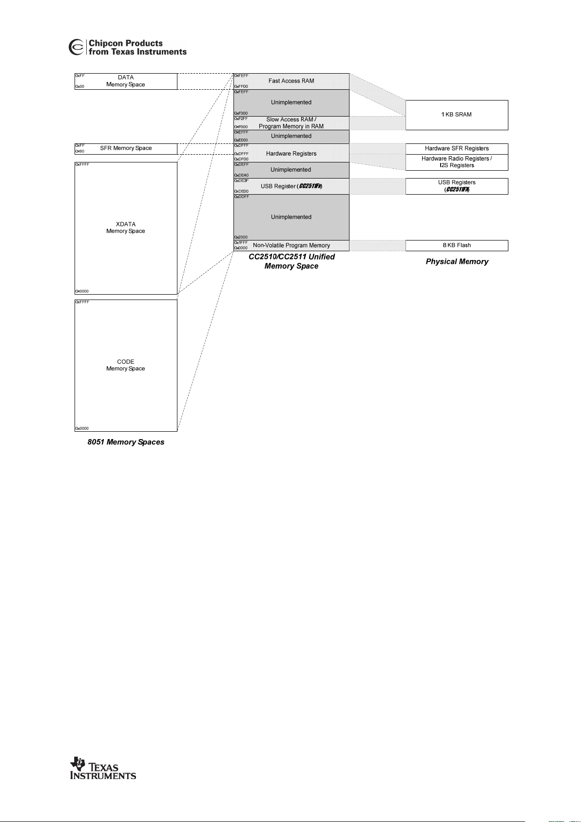
C2510Fx / CC2511Fx
SWRS055D Page 40 of 243
Figure 14:
CC2510F8/CC2511F8
Memory Mapping

C2510Fx / CC2511Fx
SWRS055D Page 41 of 243
Figure 15:
CC2510F16/CC2511F16
Memory Mapping

C2510Fx / CC2511Fx
SWRS055D Page 42 of 243
Figure 16:
CC2510F32/CC2511F32
Memory Mapping
Details about the mapping of all 8051 memory
spaces are given in the next section.
11.2.2 8051 Memory Space
This section describes the details of each
standard 8051 memory space. Any differences
between the standard 8051 and
CC2510Fx/CC2511Fx
is described.
11.2.2.1 XDATA Memory Space
On a standard 8051 this memory space would
hold any extra RAM available.
The 8, 16, and 32 KB flash program memory is
mapped into the address ranges 0x0000 0x1FFF, 0x0000 - 0x3FFF, and 0x0000 0x7FFF respectively.
The
CC2510Fx/CC2511Fx
has a total of 1, 2, or 4
KB SRAM, starting at address 0xF000.
Compilers/assemblers must take into
consideration that the first address of usable
SRAM start at 0xF000 instead of 0x0000.
The 350 bytes of XDATA in location 0xFDA20xFEFF on
CC2510F32
and
CC2511F32
do not
retain data when power modes PM2 or PM3
are entered. Refer to Section 13.1.2 on Page
75 for a detailed description of power modes.
The 256 bytes from 0xFF00 to 0xFFFF are the
DATA memory space mapped to XDATA.
These bytes are also reached through the
DATA memory space.
In addition the following is mapped into the
XDATA memory space:
• Radio registers are mapped into
address range 0xDF00 - 0xDF3D.
• I
2
S registers are mapped into the
address range 0xDF40 - 0xDF48.

C2510Fx / CC2511Fx
SWRS055D Page 43 of 243
• All SFR except the registers shown in
gray in Table 30 are mapped into
address range 0xDF80-0xDFFF.
• The USB registers are mapped into the
address range 0xDE00 - 0xDE3F on the
CC2511Fx
, but are not implemented on
the
CC2510Fx
.
This memory mapping allows the DMA
controller (and the CPU) access to all the
physical memories in a single unified address
space.
Be aware that access to unimplemented areas
in the unified memory space will give an
undefined result.
11.2.2.2 CODE Memory Space
On a standard 8051 this memory space would
hold the program memory, where the MCU
reads the program/instructions.
All memory spaces are mapped into the CODE
memory space and the mapping is identical to
the XDATA memory space, hence the
CC2510Fx/CC2511Fx
has what can be referred to
as a unified memory space.
Due to this, the
CC2510Fx/CC2511Fx
allows
execution of a program stored in SRAM. This
allows the program to be easily updated
without writing to flash (which have a limited
erase/write cycles) This is particularly useful
on the
CC2511Fx
, where parts of the firmware
can be downloaded from the windows USB
driver.
Executing a program from SRAM instead of
flash will also result in a lower power
consumption and may be interesting for battery
powered devices.
11.2.2.3 DATA Memory Space
The 8-bit address range of DATA memory
space is mapped into address 0xFF00 –
0xFFFF and is accessible through the unified
memory space. Just like on a standard 8051,
the upper 128 byte share address with the
SFR and can only be accessed indirectly, the
stack is normally located here. The lower 48
bytes are reserved, and hold 4 register banks
used by the MCU. The 16 bytes on addresses
0x20 to 0x2F are bit addressable.
The DATA memory will retain its contents in all
four power modes.
11.2.2.4 SFR Memory Space
The SFR memory space is identical to a
standard 8051.
The 128 hardware SFRs are accessed through
this memory space.
Unlike on a standard 8051, the SFRs are also
accessible through the XDATA and CODE
memory space at the address range 0xDF80 0xDFFF.
Some CPU-specific SFRs reside inside the
CPU core and can only be accessed using the
SFR memory space and not through the
duplicate mapping into XDATA/CODE memory
space. These registers are shown in gray in
Table 30. Be aware that these registers can
not be accessed using DMA.
11.2.3 Physical Memory
11.2.3.1 SRAM
The
CC2510Fx/CC2511Fx
contains static RAM. At
power-on the contents of RAM is undefined.
The RAM size is 1, 2, or 4 KB in total, mapped
to the memory range 0xF000 – 0xFFFF. In the
F8 version, memory range 0xF400 - 0xFFFF is
unimplemented while on the F16 version,
memory range 0xF800 – 0xFFFF is
unimplemented.
The memory locations 0xFDA2 - 0xFEFF
consisting of 350 bytes in unified memory
space do not retain data when power modes
PM2 or PM3 is entered. All other RAM memory
locations are retained in all power modes.
11.2.3.2 Flash Memory
The on-chip flash memory consists of 8192,
16384, or 32768 bytes (F8, F16, and F32). The
flash memory is primarily intended to hold
program code. The flash memory has the
following features:
• Flash page erase time: 20 ms
• Flash chip (mass) erase time: 200 ms
• Flash write time (2 bytes): 20 µs
• Data retention (at room temperature):
100 years
• Program/erase endurance: Minimum
1,000 cycles
The flash memory consists of the Flash Main
Pages (up to 32 times 1 KB) which is where
the CPU reads program code and data. The
flash memory also contains a Flash

C2510Fx / CC2511Fx
SWRS055D Page 44 of 243
Information Page (1 KB) which contains the
Flash Lock Bits. The lock protect bits are
written as a normal flash write to FWDATA but
the Debug Interface needs to select the Flash
Information Page first instead of the Flash
Main Page. The Information Page is selected
through the Debug Configuration which is
written through the Debug Interface only. The
Flash Controller (see Section 13.3) is used to
write and erase the contents of the flash main
memory.
When the CPU reads instructions from flash
memory, it fetches the next instruction through
a cache. The instruction cache is provided
mainly to reduce power consumption by
reducing the amount of time the flash memory
itself is accessed. The use of the instruction
cache may be disabled with the
MEMCTR.CACHDIS register bit, but doing so
will increase power consumption.
11.2.3.3 Special Function Registers
The Special Function Registers (SFRs) control
several of the features of the 8051 CPU core
and/or peripherals. Many of the 8051 core
SFRs are identical to the standard 8051 SFRs.
However, there are additional SFRs that
control features that are not available in the
standard 8051. The additional SFRs are used
to interface with the peripheral units and RF
transceiver.
Table 30 shows the address to all SFRs in
CC2510Fx/CC2511Fx
. The 8051 internal SFRs are
shown with grey background, while the other
SFRs are specific to
CC2510Fx/CC2511Fx
.
Note: All internal SFRs (shown with grey
background in Table 30, can only be accessed
through SFR memory space as these registers
are not mapped into XDATA memory space.
Table 31 lists the additional SFRs that are not
standard 8051 peripheral SFRs or CPUinternal SFRs. The additional SFRs are
described in the relevant sections for each
peripheral function.
8 Bytes
80 P0 SP DPL0 DPH0 DPL1 DPH1 U0CSR PCON 87
88 TCON P0IFG P1IFG P2IFG PICTL P1IEN P0INP 8F
90 P1 RFIM DPS MPAGE ENDIAN 97
98 S0CON IEN2 S1CON T2CT T2PR T2CTL 9F
A0 P2 WORIRQ WORCTRL WOREVT0 WOREVT1 WORTIME0 WORTIME1 A7
A8 IEN0 IP0 FWT FADDRL FADDRH FCTL FWDATA AF
B0 ENCDI ENCDO ENCCS ADCCON1 ADCCON2 ADCCON3 B7
B8 IEN1 IP1 ADCL ADCH RNDL RNDH SLEEP BF
C0 IRCON U0DBUF U0BAUD U0UCR U0GCR CLKCON MEMCTR C7
C8 WDCTL T3CNT T3CTL T3CCTL0 T3CC0 T3CCTL1 T3CC1 CF
D0 PSW DMAIRQ DMA1CFGL DMA1CFGH DMA0CFGL DMA0CFGH DMAARM DMAREQ D7
D8 TIMIF RFD T1CC0L T1CC0H T1CC1L T1CC1H T1CC2L T1CC2H DF
E0 ACC RFST T1CNTL T1CNTH T1CTL T1CCTL0 T1CCTL1 T1CCTL2 E7
E8 IRCON2 RFIF T4CNT T4CTL T4CCTL0 T4CC0 T4CCTL1 T4CC1 EF
F0 B PERCFG ADCCFG P0SEL P1SEL P2SEL P1INP P2INP F7
F8 U1CSR U1DBUF U1BAUD U1UCR U1GCR P0DIR P1DIR P2DIR FF
Table 30: SFR Address Overview

C2510Fx / CC2511Fx
SWRS055D Page 45 of 243
Register
Name
SFR
Address
Module Description Retention5
ADCCON1 0xB4 ADC ADC Control 1 Y
ADCCON2 0xB5 ADC ADC Control 2 Y
ADCCON3 0xB6 ADC ADC Control 3 Y
ADCL 0xBA ADC ADC Data Low Y
ADCH 0xBB ADC ADC Data High Y
RNDL 0xBC ADC Random Number Generator Data Low Y
RNDH 0xBD ADC Random Number Generator Data High Y
ENCDI 0xB1 AES Encryption/Decryption Input Data N
ENCDO 0xB2 AES Encryption/Decryption Output Data N
ENCCS 0xB3 AES Encryption/Decryption Control and Status N
DMAIRQ 0xD1 DMA DMA Interrupt Flag Y
DMA1CFGL 0xD2 DMA DMA Channel 1-4 Configuration Address Low Y
DMA1CFGH 0xD3 DMA DMA Channel 1-4 Configuration Address High Y
DMA0CFGL 0xD4 DMA DMA Channel 0 Configuration Address Low Y
DMA0CFGH 0xD5 DMA DMA Channel 0 Configuration Address High Y
DMAARM 0xD6 DMA DMA Channel Arm Y
DMAREQ 0xD7 DMA DMA Channel Start Request and Status Y
FWT 0xAB FLASH Flash Write Timing Y
FADDRL 0xAC FLASH Flash Address Low Y
FADDRH 0xAD FLASH Flash Address High Y
FCTL 0xAE FLASH Flash Control [7:1]Y, [1:0]N
FWDATA 0xAF FLASH Flash Write Data Y
P0IFG 0x89 IOC Port 0 Interrupt Status Flag Y
P1IFG 0x8A IOC Port 1 Interrupt Status Flag Y
P2IFG 0x8B IOC Port 2 Interrupt Status Flag Y
PICTL 0x8C IOC Port Pins Interrupt Mask and Edge Y
P1IEN 0x8D IOC Port 1 Interrupt Mask Y
P0INP 0x8F IOC Port 0 Input Mode Y
PERCFG 0xF1 IOC Peripheral I/O Control Y
ADCCFG 0xF2 IOC ADC Input Configuration Y
P0SEL 0xF3 IOC Port 0 Function Select Y
P1SEL 0xF4 IOC Port 1 Function Select Y
P2SEL 0xF5 IOC Port 2 Function Select Y
P1INP 0xF6 IOC Port 1 Input Mode Y
P2INP 0xF7 IOC Port 2 Input Mode Y
P0DIR 0xFD IOC Port 0 Direction Y
P1DIR 0xFE IOC Port 1 Direction Y
P2DIR 0xFF IOC Port 2 Direction Y
MEMCTR 0xC7 MEMORY Memory System Control Y
5
Registers without retention are in their reset state after PM2 or PM3. This is only applicable for
registers / bits that are defined as R/W

C2510Fx / CC2511Fx
SWRS055D Page 46 of 243
Register
Name
SFR
Address
Module Description Retention5
SLEEP 0xBE PMC Sleep Mode Control [6:2]Y, [7,1:0]N
CLKCON 0xC6 PMC Clock Control Y
RFIM 0x91 RF RF Interrupt Mask Y
RFD 0xD9 RF RF Data N
RFIF 0xE9 RF RF Interrupt flags Y
RFST 0xE1 RF RF Strobe Commands NA
WORIRQ 0xA1 Sleep Timer Sleep Timer Interrupts Y
WORCTRL 0xA2 Sleep Timer Sleep Timer Control Y
WOREVT0 0xA3 Sleep Timer Sleep Timer Event 0 Timeout Low Byte Y
WOREVT1 0xA5 Sleep Timer Sleep Timer Event 0 Timeout High Byte Y
WORTIME0 0xA4 Sleep Timer Sleep Timer Low Byte Y
WORTIME1 0xA6 Sleep Timer Sleep Timer High Byte Y
T1CC0L 0xDA Timer1 Timer 1 Channel 0 Capture/Compare Value Low Y
T1CC0H 0xDB Timer1 Timer 1 Channel 0 Capture/Compare Value High Y
T1CC1L 0xDC Timer1 Timer 1 Channel 1 Capture/Compare Value Low Y
T1CC1H 0xDD Timer1 Timer 1 Channel 1 Capture/Compare Value High Y
T1CC2L 0xDE Timer1 Timer 1 Channel 2 Capture/Compare Value Low Y
T1CC2H 0xDF Timer1 Timer 1 Channel 2 Capture/Compare Value High Y
T1CNTL 0xE2 Timer1 Timer 1 Counter Low Y
T1CNTH 0xE3 Timer1 Timer 1 Counter High Y
T1CTL 0xE4 Timer1 Timer 1 Control and Status Y
T1CCTL0 0xE5 Timer1 Timer 1 Channel 0 Capture/Compare Control Y
T1CCTL1 0xE6 Timer1 Timer 1 Channel 1 Capture/Compare Control Y
T1CCTL2 0xE7 Timer1 Timer 1 Channel 2 Capture/Compare Control Y
T2CT 0x9C Timer2 Timer 2 Timer Count N
T2PR 0x9D Timer2 Timer 2 Prescaler N
T2CTL 0x9E Timer2 Timer 2 Control N
T3CNT 0xCA Timer3 Timer 3 Counter Y
T3CTL 0xCB Timer3 Timer 3 Control Y,[2]N
T3CCTL0 0xCC Timer3 Timer 3 Channel 0 Capture/Compare Control Y
T3CC0 0xCD Timer3 Timer 3 Channel 0 Capture/Compare Value Y
T3CCTL1 0xCE Timer3 Timer 3 Channel 1 Capture/Compare Control Y
T3CC1 0xCF Timer3 Timer 3 Channel 1 Capture/Compare Value Y
T4CNT 0xEA Timer4 Timer 4 Counter Y
T4CTL 0xEB Timer4 Timer 4 Control Y,[2]N
T4CCTL0 0xEC Timer4 Timer 4 Channel 0 Capture/Compare Control Y
T4CC0 0xED Timer4 Timer 4 Channel 0 Capture/Compare Value Y
T4CCTL1 0xEE Timer4 Timer 4 Channel 1 Capture/Compare Control Y
T4CC1 0xEF Timer4 Timer 4 Channel 1 Capture/Compare Value Y
TIMIF 0xD8 TMINT Timers 1/3/4 Joint Interrupt Mask/Flags Y
U0CSR 0x86 USART0 USART 0 Control and Status Y
U0DBUF 0xC1 USART0 USART 0 Receive/Transmit Data Buffer Y

C2510Fx / CC2511Fx
SWRS055D Page 47 of 243
Register
Name
SFR
Address
Module Description Retention5
U0BAUD 0xC2 USART0 USART 0 Baud Rate Control Y
U0UCR 0xC4 USART0 USART 0 UART Control Y,[7]N
U0GCR 0xC5 USART0 USART 0 Generic Control Y
U1CSR 0xF8 USART1 USART 1 Control and Status Y
U1DBUF 0xF9 USART1 USART 1 Receive/Transmit Data Buffer Y
U1BAUD 0xFA USART1 USART 1 Baud Rate Control Y
U1UCR 0xFB USART1 USART 1 UART Control Y,[7]N
U1GCR 0xFC USART1 USART 1 Generic Control Y
ENDIAN 0x95 MEMORY
USB Endianess Control (
CC2511Fx
)
Y
WDCTL 0xC9 WDT Watchdog Timer Control Y
Table 31: CC2510Fx/CC2511Fx Specific SFR Overview
11.2.3.4 Radio Registers
The radio registers are all related to Radio
configuration and control. The RF registers can
only be accessed through XDATA memory
space and reside in address range 0xDF00 0xDF3D.
Table 32 gives a descriptive overview of these
registers. Each register is described in detail in
Section 14.18, starting on Page 213.
XDATA
Address
Register Description Retention6
0xDF00 SYNC1 Sync word, high byte Y
0xDF01 SYNC0 Sync word, low byte Y
0xDF02 PKTLEN Packet length Y
0xDF03 PKTCTRL1 Packet automation control Y
0xDF04 PKTCTRL0 Packet automation control Y
0xDF05 ADDR Device address Y
0xDF06 CHANNR Channel number Y
0xDF07 FSCTRL1 Frequency synthesizer control Y
0xDF08 FSCTRL0 Frequency synthesizer control Y
0xDF09 FREQ2 Frequency control word, high byte Y
0xDF0A FREQ1 Frequency control word, middle byte Y
0xDF0B FREQ0 Frequency control word, low byte Y
0xDF0C MDMCFG4 Modem configuration Y
0xDF0D MDMCFG3 Modem configuration Y
0xDF0E MDMCFG2 Modem configuration Y
0xDF0F MDMCFG1 Modem configuration Y
0xDF10 MDMCFG0 Modem configuration Y
0xDF11 DEVIATN Modem deviation setting Y
0xDF12 MCSM2 Main Radio Control State Machine configuration Y
6
Registers without retention are in their reset state after PM2 or PM3. This is only applicable for
registers / bits that are defined as R/W

C2510Fx / CC2511Fx
SWRS055D Page 48 of 243
XDATA
Address
Register Description Retention6
0xDF13 MCSM1 Main Radio Control State Machine configuration Y
0xDF14 MCSM0 Main Radio Control State Machine configuration Y
0xDF15 FOCCFG Frequency Offset Compensation configuration Y
0xDF16 BSCFG Bit Synchronization configuration Y
0xDF17 AGCTRL2 AGC control Y
0xDF18 AGCTRL1 AGC control Y
0xDF19 AGCTRL0 AGC control Y
0xDF1A FREND1 Front end RX configuration Y
0xDF1B FREND0 Front end TX configuration Y
0xDF1C FSCAL3 Frequency synthesizer calibration N
0xDF1D FSCAL2 Frequency synthesizer calibration N
0xDF1E FSCAL1 Frequency synthesizer calibration N
0xDF1F FSCAL0 Frequency synthesizer calibration Y
0xDF20
0xDF22
Reserved Y
0xDF23 TEST2 Various Test Settings Y
0xDF24 TEST1 Various Test Settings Y
0xDF25 TEST0 Various Test Settings Y
0xDF27
0xDF2D
Reserved Y
0xDF2E PA_TABLE0 PA output power setting Y
0xDF2F IOCFG2 Radio test signal configuration (P1_7) Y
0xDF30 IOCFG1 Radio test signal configuration (P1_6) Y
0xDF31 IOCFG0 Radio test signal configuration (P1_5) Y
0xDF36 PARTNUM Chip ID[16:8] NA
0xDF37 VERSION Chip ID[7:0] NA
0xDF38 FREQEST Frequency Offset Estimate NA
0xDF39 LQI Link Quality Indicator NA
0xDF3A RSSI Received Signal Strength Indication NA
0xDF3B MARCSTATE Main Radio Control State NA
0xDF3C PKSTATUS Packet status NA
0xDF3D VCO_VC_DAC PLL calibration current NA
Table 32: Overview of RF Registers
11.2.3.5 I
2
S Registers
The I
2
S registers are all related to I2S
configuration and control. The I
2
S registers can
only be accessed through XDATA memory
space and reside in address range 0xDF40 -
0xDF48. Table 33 gives a descriptive overview
of these registers. Each register is described in
detail in Section 13.15.13, starting on Page
167.
XDATA
Address
Register Description Retention7

C2510Fx / CC2511Fx
SWRS055D Page 49 of 243
XDATA
Address
Register Description Retention7
0xDF40 I2SCFG0 I2S Configuration Register 0 Y
0xDF41 I2SCFG1 I2S Configuration Register 1 Y
0xDF42 I2SDATL I2S Data Low Byte N
0xDF43 I2SDATH I2S Data High Byte N
0xDF44 I2SWCNT I2S Word Count Register NA
0xDF45 I2SSTAT I2S Status Register NA
0xDF46 I2SCLKF0 I2S Clock Configuration Register 0 Y
0xDF47 I2SCLKF1 I2S Clock Configuration Register 1 Y
0xDF48 I2SCLKF2 I2S Clock Configuration Register 2 Y
Table 33: Overview of I2S Registers
11.2.3.6 USB Registers
The USB registers are all related to USB
configuration and control. The USB registers
can only be accessed through XDATA
memory space and reside in address range
0xDE00 - 0xDE3F. These registers can be
divided into three groups: The Common USB
Registers (Table 34), The Indexed Endpoint
Registers (Table 35), and the Endpoint FIFO
Registers (Table 36). Each register is
described in detail in Section 13.16.11, starting
on Page 179. Notice that the upper register
addresses 0xDE2C – 0xDE3F are reserved.
XDATA
Address
Register Description
0xDE00 USBADDR Function Address
0xDE01 USBPOW Power/Control Register
0xDE02 USBIIF IN Endpoints and EP0 Interrupt Flags
0xDE03 Reserved
0xDE04 USBOIF OUT Endpoints Interrupt Flags
0xDE05 Reserved
0xDE06 USBCIF Common USB Interrupt Flags
0xDE07 USBIIE IN Endpoints and EP0 Interrupt Enable Mask
0xDE08 Reserved
0xDE09 USBOIE Out Endpoints Interrupt Enable Mask
0xDE0A Reserved
0xDE0B USBCIE Common USB Interrupt Enable Mask
0xDE0C USBFRML Current Frame Number (Low byte)
0xDE0D USBFRMH Current Frame Number (High byte)
0xDE0E USBINDEX
Selects current endpoint. Make sure this register has the required value before any of the
registers in Table 35 are accessed. This register must be set to a value in the range 0 – 5.
Table 34: Overview of Common USB Registers
Note: All USB registers lose data in PM2
and PM3, meaning that these power
modes cannot be used on the
CC2511Fx

C2510Fx / CC2511Fx
SWRS055D Page 50 of 243
XDATA
Address
Register Description Valid USBINDEX
Value(s)
0xDE10 USBMAXI Max. packet size for IN endpoint 1 – 5
USBCS0 EP0 Control and Status (USBINDEX = 0) 0
0xDE11
USBCSIL IN EP{1-5} Control and Status Low 1 – 5
0xDE12 USBCSIH IN EP{1-5} Control and Status High 1 – 5
0xDE13 USBMAXO Max. packet size for OUT endpoint 1 – 5
0xDE14 USBCSOL OUT EP{1-5} Control and Status Low 1 – 5
0xDE15 USBCSOH OUT EP{1-5} Control and Status High 1 – 5
USBCNT0 Number of received bytes in EP0 FIFO (USBINDEX = 0) 0
0xDE16
USBCNTL Number of bytes in OUT FIFO Low 1 – 5
0xDE17 USBCNTH Number of bytes in OUT FIFO High 1 – 5
Table 35: Overview of Indexed Endpoint Registers
C2510Fx / CC2511Fx
SWRS055D Page 51 of 243
XDATA
Address
Register Description
0xDE20 USBF0 Endpoint 0 FIFO
0xDE22 USBF1 Endpoint 1 FIFO
0xDE24 USBF2 Endpoint 2 FIFO
0xDE26 USBF3 Endpoint 3 FIFO
0xDE28 USBF4 Endpoint 4 FIFO
0xDE2A USBF5 Endpoint 5 FIFO
Table 36: Overview of Endpoint FIFO Registers
11.2.4 XDATA Memory Access
The
CC2510Fx/CC2511Fx
provides an additional
SFR named MPAGE. This register is used
during instructions MOVX A,@Ri and MOVX
@Ri,A. MPAGE gives the 8 most significant
address bits, while the register Ri gives the 8
least significant bits.
In some 8051 implementations, this type of
XDATA access is performed using P2 to give
the most significant address bits. Existing
software may therefore have to be adapted to
make use of MPAGE instead of P2.
MPAGE (0x93) – Memory Page Select
Bit Name Reset R/W Description
7:0 MPAGE[7:0] 0x00 R/W Memory page, high-order bits of address in MOVX instruction
11.2.5 Memory Arbiter
The
CC2510Fx/CC2511Fx
includes a memory
arbiter which handles CPU and DMA access to
all memory space.
A control register MEMCTR is used to control
the flash cache. The MEMCTR register is
described below.
MEMCTR (0xC7) – Memory Arbiter Control
Bit Name Reset R/W Description
7:2
0 R/W Not used
Flash cache disable. Invalidates contents of instruction cache and forces all
instruction read accesses to read straight from flash memory. Disabling will
increase power consumption and is provided for debug purposes.
0 Cache enabled
1
CACHDIS
0 R/W
1 Cache disabled
Flash prefetch disable. When set prefetch of flash data is disabled, when
cleared the next two bytes in flash are fetched when last byte in cache is
read.
0 Prefetch enabled
0
PREFDIS
1 R/W
1 Prefetch disabled

C2510Fx / CC2511Fx
SWRS055D Page 52 of 243
11.3 CPU Registers
This section describes the internal registers
found in the CPU.
11.3.1 Data Pointers
The
CC2510Fx/CC2511Fx
has two data pointers,
DPTR0 and DPTR1, to accelerate the
movement of data blocks to/from memory. The
data pointers are generally used to access
CODE or XDATA space e.g.
MOVC A,@A+DPTR
MOV A,@DPTR.
The data pointer select bit, bit 0 in the Data
Pointer Select register DPS, chooses which
data pointer to use during the execution of an
instruction that uses the data pointer, e.g. in
one of the above instructions.
The data pointers are two bytes wide
consisting of the following SFRs:
• DPTR0 – DPH0:DPL0
• DPTR1 – DPH1:DPL1
DPH0 (0x83) – Data Pointer 0 High Byte
Bit Name Reset R/W Description
7:0 DPH0[7:0] 0 R/W Data pointer 0, high byte
DPL0 (0x82) – Data Pointer 0 Low Byte
Bit Name Reset R/W Description
7:0 DPL0[7:0] 0 R/W Data pointer 0, low byte
DPH1 (0x85) – Data Pointer 1 High Byte
Bit Name Reset R/W Description
7:0 DPH1[7:0] 0 R/W Data pointer 1, high byte
DPL1 (0x84) – Data Pointer 1 Low Byte
Bit Name Reset R/W Description
7:0 DPL1[7:0] 0 R/W Data pointer 1, low byte
DPS (0x92) – Data Pointer Select
Bit Name Reset R/W Description
7:1 0 R/W Not used
Data pointer select
0 DPTR0
0 DPS 0 R/W
1 DPTR1
11.3.2 Registers R0 - R7
The
CC2510Fx/CC2511Fx
provides four register
banks of eight registers each. These register
banks are in the DATA memory space at
addresses 0x00-0x07, 0x08-0x0F, 0x10-0x17
and 0x18-0x1F and are mapped to address
range 0xFF00 to 0xFF1F in the unified
memory space. Each register bank contains
the eight 8-bit register R0 - R7. The register
bank to be used is selected through the
Program Status Word PSW.RS[1:0].
11.3.3 Program Status Word
The Program Status Word (PSW) contains
several bits that show the current state of the
CPU. The Program Status Word is accessible
as an SFR and it is bit-addressable. The PSW
register contains the Carry flag, Auxiliary Carry

C2510Fx / CC2511Fx
SWRS055D Page 53 of 243
flag for BCD operations, Register Select bits,
Overflow flag, and Parity flag. Two bits in PSW
are uncommitted and can be used as userdefined status flags.
PSW (0xD0) – Program Status Word
Bit Name Reset R/W Description
7 CY 0 R/W Carry flag. Set to 1 when the last arithmetic operation resulted in a carry
(during addition) or borrow (during subtraction), otherwise cleared to 0 by all
arithmetic operations.
6 AC 0 R/W Auxiliary carry flag for BCD operations. Set to 1 when the last arithmetic
operation resulted in a carry into (during addition) or borrow from (during
subtraction) the high order nibble, otherwise cleared to 0 by all arithmetic
operations.
5 F0 0 R/W User-defined, bit-addressable
Register bank select bits. Selects which set of R7 - R0 registers to use from
four possible register banks in DATA space.
00 Bank 0, 0x00 – 0x07
01 Bank 1, 0x08 – 0x0F
10 Bank 2, 0x10 – 0x17
4:3 RS[1:0] 00 R/W
11 Bank 3, 0x18 – 0x1F
2 OV 0 R/W Overflow flag, set by arithmetic operations. Set to 1 when the last arithmetic
operation resulted in a carry (addition), borrow (subtraction), or overflow
(multiply or divide). Otherwise, the bit is cleared to 0 by all arithmetic
operations.
1 F1 0 R/W User-defined, bit-addressable
0 P 0 R/W Parity flag, parity of accumulator set by hardware to 1 if it contains an odd
number of 1’s, otherwise it is cleared to 0
11.3.4 Accumulator
ACC is the accumulator. This is the source
and destination of most arithmetic instructions,
data transfer and other instructions. The
mnemonic for the accumulator (in instructions
involving the accumulator) refers to A instead
of ACC.
ACC (0xE0) – Accumulator
Bit Name Reset R/W Description
7:0 ACC[7:0] 0x00 R/W Accumulator
11.3.5 B Register
The B register is used as the second 8-bit
argument during execution of multiply and
divide instructions. When not used for these
purposes it may be used as a scratch-pad
register to hold temporary data.
B (0xF0) – B Register
Bit Name Reset R/W Description
7:0 B[7:0] 0x00 R/W B register. Used in MUL and DIV instructions.
11.3.6 Stack Pointer
The stack resides in DATA memory space and
grows upwards. The PUSH instruction first
increments the Stack Pointer (SP) and then
copies the byte into the stack. The Stack
Pointer is initialized to 0x07 after a reset and it
is incremented once to start from location
0x08, which is the first register (R0) of the

C2510Fx / CC2511Fx
SWRS055D Page 54 of 243
second register bank. Thus, in order to use
more than one register bank, the SP should be
initialized to a different location not used for
data storage.
SP (0x81) – Stack Pointer
Bit Name Reset R/W Description
7:0 SP[7:0] 0x07 R/W Stack Pointer
11.4 Instruction Set Summary
The 8051 instruction set is summarized in
Table 37. All mnemonics copyrighted © Intel
Corporation 1980.
The following conventions are used in the
instruction set summary:
• Rn – Register R7-R0 of the currently
selected register bank.
• direct – 8-bit internal data location’s
address. This can be DATA area (0x00
– 0x7F) or SFR area (0x80 – 0xFF).
• @Ri – 8-bit internal data location, DATA
area (0x00 – 0xFF) addressed indirectly
through register R1 or R0.
• #data – 8-bit constant included in
instruction.
• #data16 – 16-bit constant included in
instruction.
• addr16 – 16-bit destination address.
Used by LCALL and LJMP. A branch
can be anywhere within the 8/16/32 KB
CODE memory space.
• addr11 – 11-bit destination address.
Used by ACALL and AJMP. The branch
will be within the same 2 KB page of
program memory as the first byte of the
following instruction.
• rel – Signed (two’s complement) 8-bit
offset byte. Used by SJMP and all
conditional jumps. Range is –128 to
+127 bytes relative to first byte of the
following instruction.
• bit – direct addressed bit in DATA area
or SFR.
The instructions that affect CPU flag settings
located in PSW are listed in Table 38 on Page
58. Note that operations on the PSW register or
bits in PSW will also affect the flag settings.
Mnemonic Description Hex
Opcode
Bytes Cycles
Arithmetic Operations
ADD A,Rn Add register to accumulator 28-2F 1 1
ADD A,direct Add direct byte to accumulator 25 2 2
ADD A,@Ri Add indirect RAM to accumulator 26-27 1 2
ADD A,#data Add immediate data to accumulator 24 2 2
ADDC A,Rn Add register to accumulator with carry flag 38-3F 1 1
ADDC A,direct Add direct byte to A with carry flag 35 2 2
ADDC A,@Ri Add indirect RAM to A with carry flag 36-37 1 2
ADDC A,#data Add immediate data to A with carry flag 34 2 2
SUBB A,Rn Subtract register from A with borrow 98-9F 1 1
SUBB A,direct Subtract direct byte from A with borrow 95 2 2
SUBB A,@Ri Subtract indirect RAM from A with borrow 96-97 1 2
SUBB A,#data Subtract immediate data from A with borrow 94 2 2
INC A Increment accumulator 04 1 1
INC Rn Increment register 08-0F 1 2
INC direct Increment direct byte 05 2 3

C2510Fx / CC2511Fx
SWRS055D Page 55 of 243
Mnemonic Description Hex
Opcode
Bytes Cycles
INC @Ri Increment indirect RAM 06-07 1 3
INC DPTR Increment data pointer A3 1 1
DEC A Decrement accumulator 14 1 1
DEC Rn Decrement register 18-1F 1 2
DEC direct Decrement direct byte 15 2 3
DEC @Ri Decrement indirect RAM 16-17 1 3
MUL AB Multiply A and B A4 1 5
DIV Divide A by B 84 1 5
DA A Decimal adjust accumulator D4 1 1
Logical Operations
ANL A,Rn AND register to accumulator 58-5F 1 1
ANL A,direct AND direct byte to accumulator 55 2 2
ANL A,@Ri AND indirect RAM to accumulator 56-57 1 2
ANL A,#data AND immediate data to accumulator 54 2 2
ANL direct,A AND accumulator to direct byte 52 2 3
ANL direct,#data AND immediate data to direct byte 53 3 4
ORL A,Rn OR register to accumulator 48-4F 1 1
ORL A,direct OR direct byte to accumulator 45 2 2
ORL A,@Ri OR indirect RAM to accumulator 46-47 1 2
ORL A,#data OR immediate data to accumulator 44 2 2
ORL direct,A OR accumulator to direct byte 42 2 3
ORL direct,#data OR immediate data to direct byte 43 3 4
XRL A,Rn Exclusive OR register to accumulator 68-6F 1 1
XRL A,direct Exclusive OR direct byte to accumulator 65 2 2
XRL A,@Ri Exclusive OR indirect RAM to accumulator 66-67 1 2
XRL A,#data Exclusive OR immediate data to accumulator 64 2 2
XRL direct,A Exclusive OR accumulator to direct byte 62 2 3
XRL direct,#data Exclusive OR immediate data to direct byte 63 3 4
CLR A Clear accumulator E4 1 1
CPL A Complement accumulator F4 1 1
RL A Rotate accumulator left 23 1 1
RLC A Rotate accumulator left through carry 33 1 1
RR A Rotate accumulator right 03 1 1
RRC A Rotate accumulator right through carry 13 1 1
SWAP A Swap nibbles within the accumulator C4 1 1
Data Transfers
MOV A,Rn Move register to accumulator E8-EF 1 1
MOV A,direct Move direct byte to accumulator E5 2 2
MOV A,@Ri Move indirect RAM to accumulator E6-E7 1 2
MOV A,#data Move immediate data to accumulator 74 2 2
MOV Rn,A Move accumulator to register F8-FF 1 2
MOV Rn,direct Move direct byte to register A8-AF 2 4

C2510Fx / CC2511Fx
SWRS055D Page 56 of 243
Mnemonic Description Hex
Opcode
Bytes Cycles
MOV Rn,#data Move immediate data to register 78-7F 2 2
MOV direct,A Move accumulator to direct byte F5 2 3
MOV direct,Rn Move register to direct byte 88-8F 2 3
MOV direct1,direct2 Move direct byte to direct byte 85 3 4
MOV direct,@Ri Move indirect RAM to direct byte 86-87 2 4
MOV direct,#data Move immediate data to direct byte 75 3 3
MOV @Ri,A Move accumulator to indirect RAM F6-F7 1 3
MOV @Ri,direct Move direct byte to indirect RAM A6-A7 2 5
MOV @Ri,#data Move immediate data to indirect RAM 76-77 2 3
MOV DPTR,#data16 Load data pointer with a 16-bit constant 90 3 3
MOVC A,@A+DPTR Move code byte relative to DPTR to accumulator 93 1 3
MOVC A,@A+PC Move code byte relative to PC to accumulator 83 1 3
MOVX A,@Ri Move external RAM (8-bit address) to A E2-E3 1 3-10
MOVX A,@DPTR Move external RAM (16-bit address) to A E0 1 3-10
MOVX @Ri,A Move A to external RAM (8-bit address) F2-F3 1 4-11
MOVX @DPTR,A Move A to external RAM (16-bit address) F0 1 4-11
PUSH direct Push direct byte onto stack C0 2 4
POP direct Pop direct byte from stack D0 2 3
XCH A,Rn Exchange register with accumulator C8-CF 1 2
XCH A,direct Exchange direct byte with accumulator C5 2 3
XCH A,@Ri Exchange indirect RAM with accumulator C6-C7 1 3
XCHD A,@Ri Exchange low-order nibble indirect. RAM with A D6-D7 1 3
Program Branching
ACALL addr11 Absolute subroutine call xxx11 2 6
LCALL addr16 Long subroutine call 12 3 6
RET Return from subroutine 22 1 4
RETI Return from interrupt 32 1 4
AJMP addr11 Absolute jump xxx01 2 3
LJMP addr16 Long jump 02 3 4
SJMP rel Short jump (relative address) 80 2 3
JMP @A+DPTR Jump indirect relative to the DPTR 73 1 2
JZ rel Jump if accumulator is zero 60 2 3
JNZ rel Jump if accumulator is not zero 70 2 3
JC rel Jump if carry flag is set to 1 40 2 3
JNC Jump if carry flag is 0 50 2 3
JB bit,rel Jump if direct bit is set to 1 20 3 4
JNB bit,rel Jump if direct bit is 0 30 3 4
JBC bit,direct rel Jump if direct bit is set to 1 and clear the bit to 0 10 3 4
CJNE A,direct rel Compare direct byte to A and jump if not equal B5 3 4
CJNE A,#data rel Compare immediate to A and jump if not equal B4 3 4
CJNE Rn,#data rel Compare immediate to reg. and jump if not equal B8-BF 3 4
CJNE @Ri,#data rel Compare immediate to indirect and jump if not equal B6-B7 3 4

C2510Fx / CC2511Fx
SWRS055D Page 57 of 243
Mnemonic Description Hex
Opcode
Bytes Cycles
DJNZ Rn,rel Decrement register and jump if not zero D8-DF 2 3
DJNZ direct,rel Decrement direct byte and jump if not zero D5 3 4
NOP No operation 00 1 1
Boolean Variable Operations
CLR C Clear carry flag C3 1 1
CLR bit Clear direct bit C2 2 3
SETB C Set carry flag to 1 D3 1 1
SETB bit Set direct bit to 1 D2 2 3
CPL C Complement carry flag B3 1 1
CPL bit Complement direct bit B2 2 3
ANL C,bit AND direct bit to carry flag 82 2 2
ANL C,/bit AND complement of direct bit to carry B0 2 2
ORL C,bit OR direct bit to carry flag 72 2 2
ORL C,/bit OR complement of direct bit to carry A0 2 2
MOV C,bit Move direct bit to carry flag A2 2 2
MOV bit,C Move carry flag to direct bit 92 2 3
Mich.
TRAP Set SW breakpoint in debug mode A5 1 1
Table 37: Instruction Set Summary

C2510Fx / CC2511Fx
SWRS055D Page 58 of 243
Instruction CY OV AC
ADD x x x
ADDC x x x
SUBB x x x
MUL 0 x -
DIV 0 x -
DA x - -
RRC x - -
RLC x - -
SETB C 1 - -
CLR C x - -
CPL C x - -
ANL C,bit x - -
ANL C,/bit x - -
ORL C,bit x - -
ORL C,/bit x - -
MOV C,bit x - -
CJNE x - -
“0” = Clear to 0, “1” = Set to 1, “x” = Set to 1/Clear to 0, “-“ = Not affected
Table 38: Instructions that Affect Flag Settings
11.5 Interrupts
The CPU has 18 interrupt sources. Each
source has its own request flag located in a
set of Interrupt Flag SFRs. Each interrupt can
be individually enabled or disabled. The
definitions of the interrupt sources and the
interrupt vectors are given in Table 39.
I
2
S and USART1 share interrupts. On the
CC2511Fx
USB shares interrupt with Port 2
inputs. The interrupt aliases for I
2
S and USB
are listed in Table 40. However, in the
following sections the original interrupt names,
masks, and flags listed in Table 39 are
the ones used.
The interrupts are grouped into a set of priority
level groups with selectable priority levels.
The interrupt enable registers are described in
Section 11.5.1 and the interrupt priority
settings are described in Section 11.5.2 on
Page 66.
11.5.1 Interrupt Masking
Each interrupt can be individually enabled or
disabled by the interrupt enable bits in the
Interrupt Enable SFRs IEN0, IEN1, and IEN2.
The Interrupt Enable SFRs are described
below and summarized in Table 39.
Note that some peripherals have several
events that can generate the interrupt request
associated with that peripheral. This applies to
P0, P1, P2, DMA, Timer 1, Timer 2, Timer 3,
Timer 4, and Radio. These peripherals have
interrupt mask bits for each internal interrupt
source in the corresponding SFRs. Note that
I
2
S has its own interrupt enable bits even if it
has only one event per interrupt. For the
peripherals that have their own mask bits, one
or more of these bits must be set for the
associated CPU interrupt flag to be asserted.
In order to use any of the interrupts in the
CC2510Fx/CC2511Fx
the following steps must be
taken:

C2510Fx / CC2511Fx
SWRS055D Page 59 of 243
1. Clear interrupt flags (see Section
11.5.2)
2. Set individual interrupt enable bit in the
peripherals SFR, if any
3. Set the corresponding individual,
interrupt enable bit in the IEN0, IEN1,
or IEN2 registers to 1
4. Enable global interrupt by setting the
IEN0.EA = 1
5. Begin the interrupt service routine at the
corresponding vector address of that
interrupt. See Table 39 for
addresses
Interrupt
Number
Description Interrupt
Name
Interrupt
Vector
CPU Interrupt
Mask
CPU Interrupt Flag
0 RF TX done / RX ready RFTXRX 0x03
IEN0.RFTXRXIE
TCON.RFTXRXIF
8
1 ADC end of conversion ADC 0x0B
IEN0.ADCIE
TCON.ADCIF
8
2 USART0 RX complete URX0 0x13
IEN0.URX0IE TCON.URX0IF
8
3 USART1 RX complete
(Note: I
2
S RX complete, see Table
40)
URX1 0x1B
IEN0.URX1IE TCON.URX1IF
8
4 AES encryption/decryption
complete
ENC 0x23
IEN0.ENCIE S0CON.ENCIF
5 Sleep Timer compare ST 0x2B
IEN0.STIE IRCON.STIF
6 Port 2 inputs
(Note: Also used for USB on
CC2511Fx,, see Table 40)
P2INT 0x33
IEN2.P2IE IRCON2.P2IF
9
7 USART0 TX complete UTX0 0x3B
IEN2.UTX0IE IRCON2.UTX0IF
8 DMA transfer complete DMA 0x43
IEN1.DMAIE IRCON.DMAIF
9 Timer 1 (16-bit)
capture/Compare/overflow
T1 0x4B
IEN1.T1IE IRCON.T1IF
8,9
10 Timer 2 (MAC Timer) overflow T2 0x53
IEN1.T2IE IRCON.T2IF
8,9
11 Timer 3 (8-bit) compare/overflow T3 0x5B
IEN1.T3IE IRCON.T3IF
8, 9
12 Timer 4 (8-bit) compare/overflow T4 0x63
IEN1.T4IE IRCON.T4IF
8, 9
13 Port 0 inputs
(Note: P0_7 interrupt used for USB
Resume interrupt on CC2511Fx)
P0INT 0x6B
IEN1.P0IE IRCON.P0IF
9
14 USART1 TX complete
(Note: I
2
S TX complete, see Table
40)
UTX1 0x73
IEN2.UTX1IE IRCON2.UTX1IF
15 Port 1 inputs P1INT 0x7B
IEN2.P1IE IRCON2.P1IF
9
16 RF general interrupts RF 0x83
IEN2.RFIE S1CON.RFIF
9
17 Watchdog overflow in timer mode WDT 0x8B
IEN2.WDTIE IRCON2.WDTIF
Table 39: Interrupts Overview

C2510Fx / CC2511Fx
SWRS055D Page 60 of 243
Interrupt
Number
Description Interrupt
Name
Interrupt
Vector
CPU Interrupt
Mask Alias
CPU Interrupt Flag
Alias
3 I2S RX complete URX1/
I2SRX
1Bh
IEN0.I2SRXIE TCON.I2SRXIF
10
6
USB Interrupt pending (
CC2511Fx
)
P2INT/
USB
33h
IEN2.USBIE IRCON2.USBIF
11
13
USB resume interrupt (
CC2511Fx
).
P0_6 and P0_7 does not exist on
CC2510Fx
. USB resume interrupt
configured like P0_7 interrupt on
CC2510Fx
P0INT 0x6B
IEN1.P0IE IRCON.P0IF
14 I2S TX complete UTX1/
I2STX
73h
IEN2.I2STXIE IRCON2.I2STXIF
10
Table 40: Shared Interrupt Vectors (I2S and USB)

C2510Fx / CC2511Fx
SWRS055D Page 61 of 243
IEN1 (0xB8) – Interrupt Enable 1 Register
Bit Name Reset R/W Description
7
0 R/W Not used
6
- R0 Not used
Port 0 interrupt enable
0 Interrupt disabled
5
P0IE
0 R/W
1 Interrupt enabled
Timer 4 interrupt enable
0 Interrupt disabled
4
T4IE
0 R/W
1 Interrupt enabled
Timer 3 interrupt enable
0 Interrupt disabled
3
T3IE
0 R/W
1 Interrupt enabled
Timer 2 interrupt enable
0 Interrupt disabled
2
T2IE
0 R/W
1 Interrupt enabled
Timer 1 interrupt enable
0 Interrupt disabled
1
T1IE
0 R/W
1 Interrupt enabled
DMA transfer interrupt enable
0 Interrupt disabled
0
DMAIE
0 R/W
1 Interrupt enabled

C2510Fx / CC2511Fx
SWRS055D Page 62 of 243
IEN2 (0x9A) – Interrupt Enable 2 Register
Bit Name Reset R/W Description
7:6
0 R/W Not used
Watchdog timer interrupt enable
0 Interrupt disabled
5
WDTIE
0 R/W
1 Interrupt enabled
Port 1 interrupt enable
0 Interrupt disabled
4
P1IE
0 R/W
1 Interrupt enabled
USART1 TX interrupt enable / I2S TX interrupt enable
0 Interrupt disabled
3
UTX1IE /
I2STXIE
0 R/W
1 Interrupt enabled
USART0 TX interrupt enable
0 Interrupt disabled
2
UTX0IE
0 R/W
1 Interrupt enabled
Port 2 interrupt enable (Also used for USB interrupt enable on
CC2511Fx
)
0 Interrupt disabled
1
P2IE /
USBIE
0 R/W
1 Interrupt enabled
RF general interrupt enable
0 Interrupt disabled
0
RFIE
0 R/W
1 Interrupt enabled
11.5.2 Interrupt Processing
When an interrupt occurs, the CPU will vector
to the interrupt vector address shown in Table
39, if this particular interrupt has been
enabled. Once an interrupt service has begun,
it can be interrupted only by a higher priority
interrupt. The interrupt service is terminated by
a RETI (return from interrupt) instruction.
When a RETI is performed, the CPU will return
to the instruction that would have been next
when the interrupt occurred.
When the interrupt condition occurs, an
interrupt flag bit will be set in one of the CPU
interrupt flag registers and in the peripherals
interrupt flag register, if this is available. These
bits are asserted regardless of whether the
interrupt is enabled or disabled. If the interrupt
is enabled when an interrupt flag is asserted,
then on the next instruction cycle the interrupt
will be acknowledged by hardware forcing an
LCALL to the appropriate vector address.
Interrupt response will require a varying
amount of time depending on the state of the
CPU when the interrupt occurs. If the CPU is
performing an interrupt service with equal or
greater priority, the new interrupt will be
pending until it becomes the interrupt with
highest priority. In other cases, the response
time depends on the current instruction. The
fastest possible response to an interrupt is
seven instruction cycles. This includes one
machine cycle for detecting the interrupt and
six cycles to perform the LCALL.
Clearing interrupt flags must be done correctly
to ensure that no interrupts are lost or
processed more than once. For pulsed or
edge shaped interrupt sources one should
clear the CPU interrupt flag prior to clearing
the module interrupt flag, if available, for flags
that are not automatically cleared. For level
triggered interrupts (port interrupts) one has to
clear the module interrupt flag prior to clearing
the CPU interrupt flag. When handling
interrupts where the CPU interrupt flag is
cleared by hardware, the software should only
clear the module interrupt flag. The following
interrupts are cleared by hardware:
• RFTXRX • T1
• ADC • T2
• URX0 • T3
• URX1/I2SRX • T4
One or more module flags can be cleared at
once. However the safest approach is to only

C2510Fx / CC2511Fx
SWRS055D Page 63 of 243
handle one interrupt source each time the
interrupt is triggered, hence clearing only one
module flag. When any module flag is cleared
the chip will check if there are any module
interrupt flags left that are both enabled and
asserted, if so the CPU interrupt flag will be
asserted and a new interrupt triggered.
The following code example shows how only
one module flag is handled and cleared each
time the interrupt occurs:
TCON (0x88) – CPU Interrupt Flag 1
Bit Name Reset R/W Description
USART1 RX interrupt flag / I2S RX interrupt flag
Set to 1 when USART1 RX interrupt occurs and cleared when CPU vectors
to the interrupt service routine.
0 Interrupt not pending
7
URX1IF /
I2SRXIF
0 R/W
H0
1 Interrupt pending
6
0 R/W Not used
ADC interrupt flag. Set to 1 when ADC interrupt occurs and cleared when
CPU vectors to the interrupt service routine.
0 Interrupt not pending
5
ADCIF
0 R/W
H0
1 Interrupt pending
4
0 R/W Not used
USART0 RX interrupt flag. Set to 1 when USART0 interrupt occurs and
cleared when CPU vectors to the interrupt service routine.
0 Interrupt not pending
3
URX0IF
0 R/W
H0
1 Interrupt pending
2
1 R/W Reserved. Must always be set to 1.
RF TX/RX complete interrupt flag. Set to 1 when RFTXRX interrupt occurs
and cleared when CPU vectors to the interrupt service routine.
0 Interrupt not pending
1
RFTXRXIF
0 R/W
H0
1 Interrupt pending
0
1 R/W Reserved. Must always be set to 1.
#pragma vector = RF_VECTOR
__interrupt void rf_interrupt (void)
{
S1CON &= ~0x03; // Clear CPU interrupt flag
if(RFIF & 0x80) // TX underflow
{
irq_txunf(); // Handle TX underflow
RFIF = ~0x80; // Clear module interrupt flag
}
else if(RFIF & 0x40) // RX overflow
{
irq_rxovf(); // Handle RX overflow
RFIF = ~0x40; // Clear module interrupt flag
}
// Use ”else if” to check and handle other RFIF flags
}

C2510Fx / CC2511Fx
SWRS055D Page 64 of 243
S0CON (0x98) – CPU Interrupt Flag 2
Bit Name Reset R/W Description
7:2
0 R/W Not used
AES interrupt. ENCIF has two interrupt flags, ENCIF_1 and ENCIF_0.
Interrupt source sets both ENCIF_1 and ENCIF_0, but setting one of these
flags in SW will generate an interrupt request. Both flags are set when the
AES co-processor requests the interrupt.
0 Interrupt not pending
1
ENCIF_1
0 R/W
1 Interrupt pending
AES interrupt. ENCIF has two interrupt flags, ENCIF_1 and ENCIF_0.
Interrupt source sets both ENCIF_1 and ENCIF_0, but setting one of these
flags in SW will generate an interrupt request. Both flags are set when the
AES co-processor requests the interrupt.
0 Interrupt not pending
0
ENCIF_0
0 R/W
1 Interrupt pending
S1CON (0x9B) – CPU Interrupt Flag 3
Bit Name Reset R/W Description
7:6
0 R/W Not used
RF general interrupt. RFIF has two interrupt flags, RFIF_1 and RFIF_0.
Interrupt source sets both RFIF_1 and RFIF_0, but setting one of these
flags in SW will generate an interrupt request. Both flags are set when the
radio requests the interrupt.
0 Interrupt not pending
1
RFIF_1
0 R/W
1 Interrupt pending
RF general interrupt. RFIF has two interrupt flags, RFIF_1 and RFIF_0.
Interrupt source sets both RFIF_1 and RFIF_0, but setting one of these
flags in SW will generate an interrupt request. Both flags are set when the
radio requests the interrupt.
0 Interrupt not pending
0
RFIF_0
0 R/W
1 Interrupt pending

C2510Fx / CC2511Fx
SWRS055D Page 65 of 243
IRCON (0xC0) – CPU Interrupt Flag 4
Bit Name Reset R/W Description
Sleep Timer interrupt flag
0 Interrupt not pending
7
STIF
0 R/W
1 Interrupt pending
6
0 R/W Reserved. Must always be set to 0. Failure to do so will lead to ISR toggling
(interrupt routine sustained)
Port 0 interrupt flag
0 Interrupt not pending
5
P0IF
0 R/W
1 Interrupt pending
Timer 4 interrupt flag. Set to 1 when Timer 4 interrupt occurs and cleared
when CPU vectors to the interrupt service routine.
0 Interrupt not pending
4
T4IF
0 R/W
H0
1 Interrupt pending
Timer 3 interrupt flag. Set to 1 when Timer 3 interrupt occurs and cleared
when CPU vectors to the interrupt service routine.
0 Interrupt not pending
3
T3IF
0 R/W
H0
1 Interrupt pending
Timer 2 interrupt flag. Set to 1 when Timer 2 interrupt occurs and cleared
when CPU vectors to the interrupt service routine.
0 Interrupt not pending
2
T2IF
0 R/W
H0
1 Interrupt pending
Timer 1 interrupt flag. Set to 1 when Timer 1 interrupt occurs and cleared
when CPU vectors to the interrupt service routine.
0 Interrupt not pending
1
T1IF
0 R/W
H0
1 Interrupt pending
DMA complete interrupt flag.
0 Interrupt not pending
0
DMAIF
0 R/W
1 Interrupt pending

C2510Fx / CC2511Fx
SWRS055D Page 66 of 243
IRCON2 (0xE8) – CPU Interrupt Flag 5
Bit Name Reset R/W Description
7:5
0 R/W Not used
Watchdog timer interrupt flag
0 Interrupt not pending
4
WDTIF
0 R/W
1 Interrupt pending
Port 1 interrupt flag.
0 Interrupt not pending
3
P1IF
0 R/W
1 Interrupt pending
USART1 TX interrupt flag / I2S TX interrupt flag
0 Interrupt not pending
2
UTX1IF /
I2STXIF
0 R/W
1 Interrupt pending
USART0 TX interrupt flag
0 Interrupt not pending
1
UTX0IF
0 R/W
1 Interrupt pending
Port2 interrupt flag / USB interrupt flag
0 Interrupt not pending
0
P2IF /
USBIF
0 R/W
1 Interrupt pending
11.5.3 Interrupt Priority
The interrupts are grouped into six interrupt
priority groups and the priority for each group
is set by the registers IP0 and IP1. The
interrupt priority groups with assigned interrupt
sources are shown in Table 42. Each group is
assigned one of four priority levels, and by
default all six interrupt priority groups are
assign the lowest priority. In order to assign a
higher priority to an interrupt, i.e. to its interrupt
group, the corresponding bits in IP0 and IP1
must be set as shown in Table 41 on Page 67.
While an interrupt service request is in
progress, it cannot be interrupted by a lower or
same level interrupt. In the case when
interrupt requests of the same priority level are
received simultaneously, the polling sequence
shown in Table 43 is used to resolve the
priority of each requests.
IP1 (0xB9) – Interrupt Priority 1
Bit Name Reset R/W Description
7:6
0 R/W Not used
5
IP1_IPG5
0 R/W Interrupt group 5, priority control bit 1, refer to Table 41
4
IP1_IPG4
0 R/W Interrupt group 4, priority control bit 1, refer to Table 41
3
IP1_IPG3
0 R/W Interrupt group 3, priority control bit 1, refer to Table 41
2
IP1_IPG2
0 R/W Interrupt group 2, priority control bit 1, refer to Table 41
1
IP1_IPG1
0 R/W Interrupt group 1, priority control bit 1, refer to Table 41
0
IP1_IPG0
0 R/W Interrupt group 0, priority control bit 1, refer to Table 41

C2510Fx / CC2511Fx
SWRS055D Page 67 of 243
IP0 (0xA9) – Interrupt Priority 0
Bit Name Reset R/W Description
7:6
0 R/W Not used
5
IP0_IPG5
0 R/W Interrupt group 5, priority control bit 0, refer to Table 41
4
IP0_IPG4
0 R/W Interrupt group 4, priority control bit 0, refer to Table 41
3
IP0_IPG3
0 R/W Interrupt group 3, priority control bit 0, refer to Table 41
2
IP0_IPG2
0 R/W Interrupt group 2, priority control bit 0, refer to Table 41
1
IP0_IPG1
0 R/W Interrupt group 1, priority control bit 0, refer to Table 41
0
IP0_IPG0
0 R/W Interrupt group 0, priority control bit 0, refer to Table 41
IP1_x IP0_x Priority Level
0 0
0 (lowest)
0 1
1
1 0
2
1 1
3 (highest)
Table 41: Priority Level Setting
Group Interrupts
IPG0 RFTXRX RF DMA
IPG1 ADC T1 P2INT / USB
IPG2 URX0 T2 UTX0
IPG3 URX1 / I2SRX T3 UTX1 / I2STX
IPG4 ENC T4 P1INT
IPG5 ST P0INT (USB Resume) WDT
Table 42: Interrupt Priority Groups

C2510Fx / CC2511Fx
SWRS055D Page 68 of 243
Interrupt Number Interrupt Name
0 RFTXRX
16 RF
8 DMA
1 ADC
9 T1
2 URX0
10 T2
3 URX1 / I2SRX
11 T3
4 ENC
12 T4
5 ST
13 P0INT / (USB Resume)
6 P2INT / USB
7 UTX0
14 URX1 / I2STX
15 P1INT
17 WDT
Polling sequence
Table 43: Interrupt Polling Sequence
12 Debug Interface
The
CC2510Fx/CC2511Fx
includes an on-chip
debug module which communicates over a
two-wire interface. The debug interface allows
programming of the on-chip flash. It also
provides access to memory and registers
contents, and debug features such as
breakpoints, single-stepping, and register
modification.
The debug interface uses the I/O pins P2_1 as
Debug Data and P2_2 as Debug Clock during
Debug mode. These I/O pins can be used as
general purpose I/O only while the device is
not in Debug mode. Thus the debug interface
does not interfere with any peripheral I/O pins.
12.1 Debug Mode
Debug mode is entered by forcing two rising
edge transitions on pin P2_2 (Debug Clock)
while the RESET_N input is held low.
While in Debug mode pin P2_1 is the Debug
Data bi-directional pin and P2_2 is the Debug
Clock input pin.
12.2 Debug Communication
The debug interface uses an SPI-like two-wire
interface consisting of the P2_1 (Debug Data)
and P2_2 (Debug Clock) pins. Data is driven
on the bi-directional Debug Data pin at the
positive edge of Debug Clock and data is
sampled on the negative edge of this clock.
Debug commands are sent by an external host
and consist of 1 to 4 output bytes (including
Note: Debugging of PM2 and PM3 is not
supported. Also note that CLKCON.CLKSPD
must be 000 or 001 when using the debug
interface

C2510Fx / CC2511Fx
SWRS055D Page 69 of 243
command byte) from the host and an optional
input byte read by the host. Command and
data is transferred with MSB first. Figure 17
shows a timing diagram of data on the debug
interface.
Figure 17: Debug Interface Timing Diagram
12.3 Debug Lock Bit
For software and/or access protection, a set of
lock bits can be written. This information is
contained in the Flash Information Page (see
Section 11.2.3.2), at location 0x000. The Flash
Information Page can only be accessed
through the debug interface. There are three
kinds of lock protect bits as described in this
section.
The lock size bits LSIZE[2:0] are used to
define which section of the flash memory
should be write protected, if any. The size of
the write protected area can be set to 0 (no
pages), 1, 2, 4, 8, 16, 24, or 32 KB (all pages),
starting from top of flash memory and defining
a section below this. Note that for
CC2510F8
,
CC2511F8, CC2510F16
, and
CC2511F16
, the only
supported value for LSIZE[2:0]is 0 and 7
(all or no pages respectively).
The second type of lock protect bits is
BBLOCK, which is used to lock the boot sector
page (page 0 ranging from address 0x0000 to
0x03FF). When BBLOCK is set to 0, the boot
sector page is locked.
The third type of lock protect bit is DBGLOCK,
which is used to disable hardware debug
support through the Debug Interface. When
DBGLOCK is set to 0, almost all debug
commands are disabled.
When the Debug Lock bit, DBGLOCK, is set to
0 (see Table 44) all debug commands except
CHIP_ERASE, READ_STATUS and
GET_CHIP_ID are disabled and will not
function. The status of the Debug Lock bit can
be read using the READ_STATUS command
(see Section 12.4.2).
Note that after the Debug Lock bit has
changed due to a Flash Information Page write
or a flash mass erase, a HALT, RESUME,
DEBUG_INSTR, STEP_INSTR, or
STEP_REPLACE command must be executed
so that the Debug Lock value returned by
READ_STATUS shows the updated Debug
Lock value. For example a dummy NOP
DEBUG_INSTR command could be executed.
The Debug Lock bit will also be updated after
a device reset so an alternative is to reset the
chip and reenter debug mode.
The CHIP_ERASE command will set all bits in
flash memory to 1. This means that after
issuing a CHIP_ERASE command the boot
sector will be writable, no pages will be writeprotected, and all debug commands are
enabled.
The lock protect bits are written as a normal
flash write to FWDATA (see Section 13.3.2), but
the Debug Interface needs to select the Flash
Information Page first instead of the Flash
Main Page which is the default setting. The
Information Page is selected through the
Debug Configuration which is written through
the Debug Interface only. Refer to Section
12.4.1 and Table 46 for details on how the
Flash Information Page is selected using the
Debug Interface.
Table 44 defines the byte containing the flash
lock protection bits. Note that this is not an
SFR, but instead the byte stored at location
0x000 in Flash Information Page.

C2510Fx / CC2511Fx
SWRS055D Page 70 of 243
Bit Name Description
7:5 Reserved, write as 0
Boot Block Lock
0 Page 0 is write protected
4 BBLOCK
1 Page 0 is writeable, unless LSIZE is 000
Lock Size. Sets the size of the upper flash area which is write-protected. Byte
sizes are listed below
000 32 KB (all pages)
001 24 KB CC2510F32 and CC2511F32 only
010 16 KB CC2510F32 and CC2511F32 only
011 8 KB CC2510F32 and CC2511F32 only
100 4 KB CC2510F32 and CC2511F32 only
101 2 KB CC2510F32 and CC2511F32 only
110 1 KB CC2510F32 and CC2511F32 only
3:1 LSIZE[2:0]
111 0 bytes (no pages)
Debug lock bit
0 Disable debug commands
0 DBGLOCK
1 Enable debug commands
Table 44: Flash Lock Protection Bits Definition
12.4 Debug Commands
The debug commands are shown in Table 45.
Some of the debug commands are described
in further detail in the following sections
12.4.1 Debug Configuration
The commands WR_CONFIG and
RD_CONFIG are used to access the debug
configuration data byte. The format and
description of this configuration data is shown
in Table 46
12.4.2 Debug Status
A debug status byte is read using the
READ_STATUS command. The format and
description of this debug status is shown in
Table 47.
The READ_STATUS command is used e.g.
for polling the status of flash chip erase after a
CHIP_ERASE command or oscillator stable
status required for debug commands HALT,
RESUME, DEBUG_INSTR, STEP_REPLACE,
and STEP_INSTR.
12.4.3 Hardware Breakpoints
The debug command SET_HW_BRKPNT is
used to set a hardware breakpoint. The
CC2510Fx/CC2511Fx
supports up to four
hardware breakpoints. When a hardware
breakpoint is enabled it will compare the CPU
address bus with the breakpoint. When a
match occurs, the CPU is halted.
When issuing the SET_HW_BRKPNT debug
command, the external host must supply three
data bytes that define the hardware
breakpoint. The hardware breakpoint itself
consists of 18 bits while three bits are used for
control purposes. The format of the three data
bytes for the SET_HW_BRKPNT command is
as follows.
The first data byte consists of the following:
Bit Description
7:5 Unused
4:3 Breakpoint number; 0 - 3
Breakpoint enable
0 Disable
2
1 Enable
1:0 Reserved. Must be 00.
The second data byte consists of bits 15 - 8 of
the hardware breakpoint while the third data
byte consists of bits 7-0 of the hardware

C2510Fx / CC2511Fx
SWRS055D Page 71 of 243
breakpoint. This means that the second and
third data byte sets the CPU CODE address
where the CPU is halted.
12.4.4 Flash Programming
Programming of the on-chip flash is performed
via the debug interface. The external host
must initially send instructions using the
DEBUG_INSTR debug command to perform
the flash programming with the Flash
Controller as described in Section 13.3.
Command Instruction Code Description
CHIP_ERASE 0001 0100 Perform flash chip erase (mass erase). The debug interface will be enabled
and no parts of flash will be write-protected after issuing this command. Do
not use any other commands than READ_STATUS until mass erase has
completed. Return 1 status byte to host
WR_CONFIG 0001 1101 Write configuration data. Return 1 status byte to host. Refer to Table 46 for
details.
RD_CONFIG 0010 0100 Read configuration data. Return value set by WR_CONFIG command
GET_PC 0010 1000 Return value of 16-bit program counter
READ_STATUS 0011 0100 Read status byte. Refer to Table 47
SET_HW_BRKPNT 0011 1011 Set hardware breakpoint
HALT 0100 0100 Halt CPU operation. Return 1 status byte to host
RESUME 0100 1100 Resume CPU operation. To run this command, the CPU must have been
halted. Return 1 status byte to host
DEBUG_INSTR 0101 01yy Run debug instruction. The supplied instruction will be executed by the CPU
without incrementing the program counter. To run this command, the CPU
must have been halted. Return 1 status byte to host.
yy: Number of bytes in the CPU instruction (see Table 37). Valid values are
01, 10, and 11
STEP_INSTR 0101 1100 Step CPU instruction. The CPU will execute the next instruction from
program memory and increment the program counter after execution. To run
this command, the CPU must have been halted. Return 1 status byte to host
STEP_REPLACE 0110 01 yy
Step and replace CPU instruction. The supplied instruction will be executed
by the CPU instead of the next instruction in program memory. The program
counter will be incremented after execution. To run this command, the CPU
must have been halted. Return 1 status byte to host.
yy: Number of bytes in the CPU instruction (see Table 37). Valid values are
01, 10, and 11
GET_CHIP_ID 0110 1000
Return value of 16-bit chip ID (PARTNUM:VERSION).
Table 45: Debug Commands

C2510Fx / CC2511Fx
SWRS055D Page 72 of 243
Bit Name Description
7:4
Not used. Must be set to 0000
Disable timer operation (Timer 1/2/3/4). This overrides the
TIMER_SUSPEND bit and its function.
0 Do not disable timers
3 TIMERS_OFF
1 Disable timers
DMA pause
0 Enable DMA transfers
2 DMA_PAUSE
1 Pause all DMA transfers
Suspend timers (Timer 1/2/3/4). Timer operation is suspended for
debug instructions and if a step instruction is a branch. If not
suspended, these instructions would result an extra timer count
during the clock cycle in which the branch is executed
0 Do not suspend timers
1 TIMER_SUSPEND
1 Suspend timers
Select Flash Information Page in order to write flash lock bits (1
KB lowest part of flash)
0 Select flash Main Page
0 SEL_FLASH_INFO_PAGE
1 Select Flash Information Page
Table 46: Debug Configuration

C2510Fx / CC2511Fx
SWRS055D Page 73 of 243
Bit Name Description
Flash chip erase done
0 Chip erase in progress
7 CHIP_ERASE_DONE
1 Chip erase done
PCON idle
0 CPU is running
6 PCON_IDLE
1 CPU is idle (clock gated)
CPU halted
0 CPU running
5 CPU_HALTED
1 CPU halted
Power Mode 0
0 Power Mode 1-3 selected
4 POWER_MODE_0
1 Power Mode 0 selected (active mode if the CPU is running)
Halt status. Returns cause of last CPU halt
0 CPU was halted by HALT debug command
3 HALT_STATUS
1 CPU was halted by software or hardware breakpoint
Debug locked. Returns value of DBGLOCK bit
0 Debug interface is not locked
2 DEBUG_LOCKED
1 Debug interface is locked
Oscillators stable. This bit represents the status of the SLEEP.XSOC_STB
and SLEEP.HFRC_STB
register bits.
0 Oscillators not stable
1 OSCILLATOR_STABLE
1 Oscillators stable
Stack overflow. This bit indicates when the CPU writes to DATA memory
space at address 0xFF, which is possibly a stack overflow
0 No stack overflow
0 STACK_OVERFLOW
1 Stack overflow
Table 47: Debug Status

C2510Fx / CC2511Fx
SWRS055D Page 74 of 243
13 Peripherals
In the following sub-sections, each
CC2510Fx/CC2511Fx
peripheral is described in
detail.
13.1 Power Management and Clocks
This section describes the Power Management
Controller. The Power Management Controller
controls the use of active mode, power modes,
and clock control.
13.1.1 Power Management Introduction
The
CC2510Fx/CC2511Fx
uses different operating
modes to allow low-power operation. Ultra-lowpower operation is obtained by turning off
power supply to modules to avoid static
(leakage) power consumption and also by
using clock gating and turning off oscillators to
reduce dynamic power consumption.
The
CC2510Fx/CC2511Fx
has one active mode
and four power modes, called PM0, PM1, PM2
and PM3, where PM3 has the lowest power
consumption. The different operating modes
are shown in Table 48.
Operating Mode High-speed Oscillator Low-speed Oscillator Digital Voltage
Regulator
CPU
A
None
A
None
B
High speed XOSC
B
Low power RCOSC
Configuration
C
HS RCOSC
C
32.768 kHz XOSC
Active B and / or C B or C On Running
PM0 B and / or C B or C On Idle
PM1 A B or C On Idle
PM2 A B or C Off Idle
PM3 A A Off Idle
Table 48: Operating Modes
Active mode: The full functional mode. The
voltage regulator to the digital core is on and
either the high speed RC oscillator or the high
speed crystal oscillator or both are running.
Either the Low power RC oscillator or the
32.768 kHz crystal oscillator is running.
PM0: Same as active mode, but the CPU is
idle, meaning that no code is being executed.
PM1: The voltage regulator to the digital part is
on. Neither the high speed crystal oscillator nor
the high speed RC oscillator is running. Either
the low power RC oscillator or the 32.768 kHz
crystal oscillator is running. The system will go
to active mode on reset or an external interrupt
or when the Sleep Timer expires.
PM2: The voltage regulator to the digital core
is turned off. Neither the high speed crystal
oscillator nor the high speed RC oscillator is
running. Either the low power RC oscillator or
the 32.768 kHz crystal oscillator is running.
The system will go to active mode on reset or
an external interrupt or when the Sleep Timer
expires. The
CC2511Fx
will lose all USB state
information when PM2 is entered. Thus, PM2
should not be used with USB.
PM3: The voltage regulator to the digital core
is turned off. None of the oscillators are
running. The system will go to active mode on
reset or an external interrupt. The
CC2511Fx
will
lose all USB state information when PM3 is
entered. Thus, PM3 should not be used with
USB.
When an external interrupt occurs in PM1,
PM2, or PM3, or a Sleep Timer interrupt occur
in PM1 and PM2, active mode will be entered
and the code will start executing from where it
entered PM1/2/(3). Any enabled interrupt will
take the device from PM0 to active mode, and
also in this case the code will start executing

C2510Fx / CC2511Fx
SWRS055D Page 75 of 243
from where it entered PM0. A reset, however,
will take the chip from any of the four power
modes to active mode, but the code will start
executing from the start of the program.
13.1.2 Active Mode and Power Modes
The different operating modes are described in
detail in the five following sections.
13.1.2.1 Active Mode
This is the full functional mode of operation
where the CPU, peripherals, and RF
transceiver are active. The voltage regulator to
the digital core is on and either the high speed
RC oscillator or the high speed crystal
oscillator or both are running together with
either the Low power RC oscillator or the
32.768 kHz crystal oscillator.
13.1.2.2 PM0
If the PCON.IDLE bit is set to 1 while in active
mode, the CPU will be idle (clock gated) until
any interrupt occur. All other peripherals will
function as normal while the CPU is halted.
13.1.2.3 PM1
In PM1, the high speed oscillators (high speed
XOSC and HS RCOSC) are powered down
thereby halting the CPU and peripherals. The
digital voltage regulator, the power-on reset,
external interrupts, the low power RC oscillator
or the 32.768 kHz crystal oscillator and Sleep
Timer peripherals are active. I/O pins retain the
I/O mode and output value set before entering
PM1. When PM1 is entered, a power down
sequence is run.
PM1 is used when the expected time until a
wakeup event is relatively short since PM1
uses a fast power down/up sequence.
13.1.2.4 PM2
PM2 has the second lowest power
consumption. In PM2, the power-on reset,
external interrupts, the low power RC oscillator
or the 32.768 kHz crystal oscillator and Sleep
Timer peripherals are active. I/O pins retain the
I/O mode and output value set before entering
PM2. The content of RAM and most registers
is preserved in this mode (see Table 31, Table
32, and Table 33). All other internal circuits are
powered down. When PM2 is entered, a power
down sequence is run.
PM2 is typically entered when using the Sleep
Timer as the wakeup event. Please see
Section 13.8.1 for minimum sleep time when
using the Sleep Timer.
13.1.2.5 PM3
In PM3 the internal voltage regulator and all
oscillators are turned off.
This power mode is used to achieve the
operating mode with the lowest power
consumption. In PM3 all internal circuits that
are powered from internal voltage regulators
are turned off.
Reset (POR, or external) and external I/O port
interrupts are the only functions that are
operating in this mode. I/O pins retain the I/O
mode and output value set before entering
PM3. A reset or external interrupt condition will
wake the device and make it enter active
mode. The content of RAM and registers is
preserved in this mode. PM3 uses the same
power down/up sequence as PM2.
PM3 is used to achieve ultra low power
consumption when waiting for an external
event.
When entering active mode from PM1, PM2, or
PM3, the high-speed oscillators, which where
running when entering PM{1_3}, are started. If
the high speed crystal oscillator is selected as
source for the system clock (CLKCON.OSC=0),
the system clock will use the HS RCOSC as
clock source until the high speed crystal
oscillator is stable (SLEEP.XOSC_STB=1).
13.1.3 Power Management Control
The required power mode is selected by the
SLEEP.MODE setting. Setting the IDLE bit in
the PCON SFR after setting the MODE bits,
makes the
CC2511Fx/CC2511Fx
enter the
selected power mode. The following procedure
must be followed to be able to safely put the
device into one of the power modes PM{1-3}:
An interrupt from port pins or Sleep Timer (not
PM3), or a power-on reset will wake the device
and bring it into active mode by resetting the
MODE bits and clear the IDLE bit. Since an
interrupt can occur before the device has
// Pseudo Code
SLEEP.MODE = PM{1-3}
NOP();
NOP();
NOP();
If (SLEEP_MODE != 0)
PCON.IDLE = 1;

C2510Fx / CC2511Fx
SWRS055D Page 76 of 243
actually entered PM{1-3}, it is necessary to
clear the MODE bits before returning from all
ISRs associated with interrupts that can be
used to wake the device from PM{1-3}. It
should be noted that all port interrupts and
Sleep Timer interrupt are blocked when
SLEEP.MODE is different from 00, thus the time
between setting SLEEP.MODE ≠ 0 and
asserting PCON.IDLE should be as short as
possible. The SLEEP.MODE will be cleared to
00 by HW when power mode is entered, thus
interrupts are enabled during power modes. All
interrupts not to be used to wake up from PM
modes must be disabled before setting
SLEEP.MODE ≠ 0.
13.1.4 Power Management Registers
This section describes the Power Management
registers. All register bits retain their previous
values when entering PM2 or PM3 unless
otherwise stated.
PCON (0x87) – Power Mode Control
Bit Name Reset R/W Description
7:2 0 R/W Not used
1 0 R0/W1 Reserved. Must be set to 0. Failure to do so will stop CPU from operating.
0 IDLE 0 R0/W1
H0
Power mode control. Writing a 1 to this bit forces
CC2510Fx/CC2511Fx
to enter
the power mode set by SLEEP.MODE. This bit is always read as 0.
All interrupt requests will clear this bit and
CC2510Fx/CC2511Fx
will reenter active
mode.
Note: See Section 13.1.3 for details on how this bit should be used.
C2510Fx / CC2511Fx
SWRS055D Page 77 of 243
SLEEP (0xBE) – Sleep Mode Control
Bit Name Reset R/W Description
USB Enable (
CC2511Fx
). This bit is unused for
CC2510Fx
0 Disable (Setting this bit to 0 will reset the USB controller)
1 Enable
7 USB_EN 0 R/W
This bit will be 0 when returning from PM2 and PM3
High speed crystal oscillator (f
XOSC
) stable status
0 Oscillator is not powered up or not yet stable
6 XOSC_STB 0 R
1 Oscillator is powered up and stable
High speed RC oscillator (HS RCOSC) stable status
0 Oscillator is not powered up or not yet stable
5 HFRC_STB 0 R
1 Oscillator is powered up and stable
Status bit indicating the cause of the last reset. If there are multiple resets, the
register will only contain the last event.
00 Power-on reset or Brown-out reset
01 External reset
4:3 RST[1:0] XX R
10 Watchdog timer reset
High speed XOSC and HS RCOSC power down setting. The bit is cleared if
the CLKCON.OSC bit is toggled. If there is a calibration in progress and the
CPU attempts to set this bit, the bit will be updated at the end of calibration.
0 Both oscillators powered up
2 OSC_PD 1 R/W
H0
1 Oscillator not selected by CLKCON.OSC bit powered down
Power mode setting
00 PM0
01 PM1
10 PM2
11 PM3
1:0 MODE[1:0] 00 R/W
These bits will be set to 00 when entering PM{1-3}.
Note: It is necessary to clear the MODE bits before returning from all ISRs
associated with interrupts that can be used to wake the device from PM{1-3}.
See Section 13.1.3 for details
13.1.5 Oscillators and Clocks
The
CC2510Fx/CC2511Fx
has one internal
system clock. The source for the system clock
can be either a high speed RC oscillator or a
high speed crystal oscillator. The crystal
oscillator for
CC2510Fx
operates at 24 - 27 MHz
while the crystal oscillator for
CC2511Fx
operates at 48 MHz. The 24 - 27 MHz clock is
used directly as the system clock for
CC2510Fx
.
On
CC2511Fx
, the 48 MHz clock is used by the
USB Controller only while a derived 24 MHz
clock is used as the system clock. The source
for the system clock is selected by the
CLKCON.OSC bit.
There is also one 32 kHz clock source that can
either be a low power RCOSC or a 32.768 kHz
crystal oscillator. This is controlled by the
CLKCON.OSC32K bit.
The choice of oscillator allows a trade-off
between high-accuracy in the case of the
crystal oscillator and low power consumption
when the RC oscillator is used. Note that
operation of the RF transceiver requires that
the high speed crystal oscillator is used.
Note: The high speed crystal oscillator
must be stable (SLEEP.XOSC_STB=1)
before usin
g
the radio.

C2510Fx / CC2511Fx
SWRS055D Page 78 of 243
13.1.5.1 High Speed Oscillators
Two high speed oscillators are present in the
device:
• High speed crystal oscillator (24 – 27
MHz for
CC2510Fx
and 48 MHz for
CC2511Fx
)
• High speed RC oscillator (12 – 13.5
MHz for
CC2510Fx
and 12 MHz for
CC2511Fx
)
The high speed crystal oscillator startup time
may be too long for some applications, and the
device can therefore run on the high speed
RCOSC until the crystal oscillator is stable.
The HS RCOSC consumes less power than
the crystal oscillator, but since it is not as
accurate as the crystal oscillator it can not be
used for RF transceiver operation.
The CLKCON.OSC bit selects the source of the
system clock (high speed crystal oscillator or
high speed RC oscillator). The system clock
will not change clock source before the
selected clock source is stable (indicated by
SLEEP.XOSC_STB and SLEEP.HFRC_STB
).
The oscillator not selected as the system clock
source, will be set in power-down mode by
setting SLEEP.OSC_PD to 1 (the default state).
Thus the HS RCOSC may be turned off when
the high speed crystal oscillator has been
selected as system clock source and vice
versa. When SLEEP.OSC_PD is 0, both
oscillators are powered up and running. Be
aware that SLEEP.OSC_PD is cleared if the
CLKCON.OSC bit is toggled.
When the high speed crystal oscillator is
selected as system clock source
(CLKCON.OSC is set to 0), the HS RCOSC will
be calibrated once. If SLEEP.OSC_PD=0, the
HS RCOSC will run on the calibrated value
once the calibration is completed (see Table
15 for initial calibration time). If
SLEEP.OSC_PD=1, the HS RCOSC will be
turned off after calibration, but the calibration
value will be stored and used when the HS
RCOSC is started again. In order to calibrate
the HS RCOSC regularly (if so found
necessary based on the drift parameters listed
in Table 15) one should switch between using
the HS RCOSC and the high speed crystal
oscillator as system clock source.
If CLKCON.OSC is set to 0 when entering
PM{1-3}, the HS RCOSC will be calibrated
once when returning to active mode.
13.1.5.2 System clock speed and radio
When the radio is to be used the system must
run on HS XOSC. The RF part will be
unaffected by the CLKCON.CLKSPD setting.
There is however parts of the RF core that
runs on the system clock affected by and this
will cause limitations in manageable data rates
in RF link. These limitations are summarized in
Table 49 below. Note that these numbers does
not apply for FEC usage. Using FEC requires
CLKCON.CLKSPD to be 000.
CLKCON
Maksimum datarate, kBaud
CLKSPD
MSK GFSK 2FSK
000
500 250 500
001
500 250 500
010
500 250 500
011
500 250 500
100
400 250 400
101
200 200 200
110
100 100 100
111
50 50 50
Table 49: System clock speed VS data rate
13.1.5.3 Low Speed Oscillators (32 kHz clock
source)
Two low speed oscillators are present in the
device:
• Low speed crystal oscillator (32.768
kHz)
• Low power RC oscillator (32 – 36 kHz
for
CC2510Fx
and 32 kHz for
CC2511Fx
)
The low speed crystal oscillator is designed to
operate at 32.768 kHz and provide a stable
clock signal for systems requiring time
accuracy. The low power RC oscillator run at
f
XOSC
/ 750 for
CC2510Fx
and f
XOSC
/ 1500 for
CC2511Fx
, when calibrated. The calibration can
only take place when the high speed crystal
oscillator is enabled and stable. The low power
RC oscillator should be used to reduce cost
and power consumption compared to the
32.768 kHz crystal oscillator solution. The two
low speed oscillators can not be operated
simultaneously.
By default, after a reset, the low power RC
oscillator is enabled and selected as the 32
kHz clock source. The RC oscillator consumes
less power, but is less accurate than the

C2510Fx / CC2511Fx
SWRS055D Page 79 of 243
32.768 kHz crystal oscillator. Refer to 7.5 and
7.6 for characteristics of these oscillators.
The CLKCON.OSC32K bit selects the source of
the 32 kHz clock. This bit must only be
changed while using the HS RCOSC as the
system clock source. When the high speed
crystal oscillator is selected and it is stable, i.e.
SLEEP.XOSC_STB is 1, calibration of the low
power RC oscillator is continuously performed.
This calibration is only performed in active
mode and PM0. The result of the calibration is
a RC clock running at 32 – 36 kHz for
CC2510Fx
and 32 kHz for
CC2511Fx
.
The low power RC oscillator calibration may
take up to 2 ms to complete. The ongoing
calibration must be completed before entering
PM1 or PM2.

C2510Fx / CC2511Fx
SWRS055D Page 80 of 243
CLKCON (0xC6) – Clock Control
Bit Name Reset R/W Description
32 kHz clock oscillator select. The HS RCOSC must be selected as system clock
source when this bit is to be changed.
0 32.768 kHz crystal oscillator
1
Low power RC oscillator (32 – 36 kHz for
CC2510Fx
and 32 kHz for
CC2511Fx
)
7 OSC32K 1 R/W
Note: This bit is not retained in PM2 and PM3. After re-entry to active mode from
one of these power modes this bit will be at the reset value 1.
System clock oscillator select.
0 High speed crystal oscillator
1 HS RC oscillator
6 OSC 1 R/W
This setting will only take effect when the selected oscillator is powered up and
stable. If the high speed crystal oscillator is not powered up, it should be enabled
by setting SLEEP.OSC_PD to 0 prior to selecting it as source. If the HS RCOSC
is to be the source and it is powered down, setting this bit will turn it on.
Timer ticks output setting. The value of TICKSPD cannot be higher than CLKSPD.
CLKCON.OSC=0
HS XOSC used as clock source
for system clock
CLKCON.OSC=1
Calibrated HS RCOSC used as
clock source for system clock
000
f
Ref
26 MHz* NA NA
001 f
Ref
/2 13 MHz* f
Ref
/2 13 MHz
010 f
Ref
/4 6.5 MHz* f
Ref
/4 6.5 MHz
011 f
Ref
/8 3.25 MHz* f
Ref
/8 3.25 MHz
100 f
Ref
/16 1.625 MHz* f
Ref
/16 1.625 MHz
101 f
Ref
/32 812.5 kHz* f
Ref
/32 812.5 kHz
110 f
Ref
/64 406.25 kHz* f
Ref
/64 406.25 kHz
111 f
Ref
/128 203.125 kHz* f
Ref
/128 203.125 kHz
5:3 TICKSPD[2:0] 001 R/W
f
Ref
= f
xosc
for
CC2510Fx
and f
Ref
= f
xosc
/2 for
CC2511Fx
Numbers above are for
CC2510Fx
with f
xosc
= 26 MHz
Clock speed setting. When a new CLKSPD value is written, the new setting is
read when the clock has changed.
CLKCON.OSC=0
HS XOSC used as clock source
for system clock
CLKCON.OSC=1
Calibrated HS RCOSC used as
clock source for system clock
000
f
Ref
26 MHz NA NA
001 f
Ref
/2 13 MHz f
Ref
/2 13 MHz
010 f
Ref
/4 6.5 MHz f
Ref
/4 6.5 MHz
011 f
Ref
/8 3.25 MHz f
Ref
/8 3.25 MHz
100 f
Ref
/16 1.625 MHz f
Ref
/16 1.625 MHz
101 f
Ref
/32 812.5 kHz f
Ref
/32 812.5 kHz
110 f
Ref
/64 406.25 kHz f
Ref
/64 406.25 kHz
111 f
Ref
/128 203.125 kHz f
Ref
/128 203.125 kHz
2:0 CLKSPD[2:0] 001 R/W
f
Ref
= f
xosc
for
CC2510Fx
and f
Ref
= f
xosc
/2 for
CC2511Fx
Numbers above are for
CC2510Fx
with f
xosc
= 26 MHz

C2510Fx / CC2511Fx
SWRS055D Page 81 of 243
13.1.6 Timer Tick Generation
The power management controller generates
a tick or enable signal for the peripheral
timers, thus acting as a prescaler for the
timers. This is a global clock division for Timer
1, Timer 2, Timer 3, and Timer 4. The tick
speed is programmed from 0.203 to 26 MHz
for
CC2510Fx
assuming a 26 MHz crystal or
from 0.1875 to 24 MHz for
CC2511Fx
by setting
the CLKCON.TICKSPD register appropriately.
13.1.7 Data Retention
In PM2 and PM3, power is removed from most
of the internal circuitry. However, parts of
SRAM will retain its contents. The content of
internal registers is also retained in PM2 and
PM3, with some exceptions (see Table 31,
Table 32, and Table 33).
The XDATA memory locations 0xF0000xFFFF (4096 bytes) retain data in PM2 and
PM3. Please note the following exception:
The XDATA memory locations 0xFDA20xFEFF (350 bytes) will lose all data when
PM2 or PM3 is entered. These locations will
contain undefined data when active mode is
re-entered.
The registers which retain their contents are
the CPU registers, peripheral registers and RF
registers, unless otherwise specified for a
given register bit field. Switching to power
modes PM2 and PM3 appears transparent to
software with the following exception:
• Watchdog timer 15-bit counter is reset
to 0x0000 when entering PM2 or PM3
13.1.8 I/O and Radio
I/O port pins P1_0 and P1_1 do not have
internal pull-up/pull-down resistors. These pins
should therefore be set as outputs or pulled
high/low externally to avoid leakage current.
To save power, the radio should be turned off
when it is not used.
13.2 Reset
The
CC2510Fx/CC2511Fx
has four reset sources.
The following events generate a reset:
• Forcing RESET_N input pin low
• A power-on reset condition
• A brown-out reset condition
• Watchdog timer reset condition
The initial conditions after a reset are as
follows:
• I/O pins are configured as inputs with
pull-up, except P1_0 and P1_1.
• CPU program counter is loaded with
0x0000 and program execution starts at
this address
• All peripheral registers are initialized to
their reset values (refer to register
descriptions)
• Watchdog timer is disabled
13.2.1 Power On Reset and Brown Out
Detector
The
CC2510Fx/CC2511Fx
includes a Power On
Reset (POR) providing correct initialization
during device power-on. Also included is a
Brown Out Detector (BOD) operating on the
regulated 1.8 V digital power supply only, The
BOD will protect the memory contents during
supply voltage variations which cause the
regulated 1.8 V power to drop below the
minimum level required by flash memory and
SRAM.
When power is initially applied to the
CC2510Fx/CC2511Fx
the Power On Reset (POR)
and Brown Out Detector (BOD) will hold the
device in reset state until the supply voltage
reaches above the Power On Reset and
Brown Out voltages.
Figure 18 shows the POR/BOD operation with
the 1.8V (typical) regulated supply voltage
together with the active low reset signals
BOD_RESET and POR_RESET shown in the
bottom of the figure (note that these signals
are not available but are included on the figure
for illustration purposes).
The cause of the last reset can read from the
register bits SLEEP.RST. It should be noted
that a BOD reset will be read as a POR reset.
Note: CLKCON.TICKSPD cannot be set
higher than CLKCON.CLKSPD.

C2510Fx / CC2511Fx
SWRS055D Page 82 of 243
0
UNREGULATED
1.8V REGULATED
POR RESET ASSERT FALLING VDD
BOD RESET ASSERT
POR RESET DEASSERT RISING VDD
VOLT
POR OUTPUT
BOD RESET
POR RESET
X
X
X
X
X
X
Figure 18: Power-On-Reset and Brown Out Detector Operation
13.3 Flash Controller
The
CC2510Fx/CC2511Fx
contains 8, 16 or 32 KB
flash memory for storage of program code.
The flash memory is programmable from the
user software and through the debug interface.
See Table 27 on Page 31 for flash memory
size options.
The Flash Controller handles writing to the
embedded flash memory and erasing of the
same memory. The embedded flash memory
consists of 8, 16, or 32 pages (each page is
1024 bytes) depending on the total flash size.
The Flash Controller has the following
features:
• 16-bit word programmable
• Page erase
• Lock bits for write-protection and code
security
• Flash page erase time: 20 ms
• Flash chip erase time: 200 ms
• Flash write time (2 bytes): 20 µs
• Auto power-down during low-frequency
CPU clock read access (divided clock
source, CLKCON.CLKSPD)
13.3.1 Flash Memory Organization
The flash memory is divided into 8, 16, or 32
flash pages consisting of 1 KB each. A flash
page is the smallest erasable unit in the
memory, while a 16-bit word is the smallest
writable unit that may be addressed through
the Flash Controller.
When performing write operations, the flash
memory is word-addressable using a 14-bit
address written to the address registers
FADDRH:FADDRL.
When performing page erase operations, the
flash memory page to be erased is addressed
through the register bits FADDRH[5:1].
Note the difference in addressing the flash
memory; when accessed by the CPU to read
code or data, the flash memory is byteaddressable. When accessed by the Flash
Controller, the flash memory is wordaddressable, where a word consists of 16 bits.
The next sections describe the procedures for
flash write and flash page erase in detail.
13.3.2 Flash Write
Data is written to the flash memory by using a
program command initiated by writing a 1 to
FCTL.WRITE. Flash write operations can
program any number of words in the flash
memory, single words or block of words in
sequence starting at the address set by
FADDRH:FADDRL. A bit in a word can be
change from 1 to 0, but not from 0 - 1 (writing a
1 to a bit that is 0 will be ignored). The only
way to change a 0 to a 1 is by doing a page
erase or chip erase through the debug
interface, as the erased bits are set to 1.
A write operation is performed using one out of
two methods;
• Through DMA transfer
• Through CPU SFR access
The DMA transfer method is the preferred way
to write to the flash memory.

C2510Fx / CC2511Fx
SWRS055D Page 83 of 243
A write operation is initiated by writing a 1 to
FCTL.WRITE. The address to start writing at is
given by FADDRH:FADDRL. During each single
write operation FCTL.SWBSY is set high.
During a write operation, the data written to the
FWDATA register is forwarded to the flash
memory. The flash memory is 16-bit wordprogrammable, meaning data is written as 16bit words. The first byte written to FWDATA is
the LSB of the 16-bit word. The actual writing
to flash memory takes place each time two
bytes have been written to FWDATA, meaning
that the number of bytes written to flash must
be a multiple of two.
0x0000 0x0001
0x03FE 0x03FF
0x0800 0x0801
0x0BFF
0x7C01
0x7FFF
0x7C00
0x7FFE
0x0BFE
PAGE 0
PAGE 2
PAGE 32
.
.
.
.
.
.
.
.
.
.
.
.
.
.
.
.
.
.
Figure 19: Flash Address (in unified memory
space)
When accessed by the Flash Controller, the
flash memory is word-addressable. Each page
in flash consists of 512 words, addressed
through FADDRH[0]:FADDRL[7:0].
FADDRH[5:1] is used to indicate the page
number. That means that if one wants to write
to the byte in flash mapped to address 0x0BFE
(see Figure 19), FADDRH:FADDRL should be
0x05FF (page 2, word 511).
The CPU will not be able to access the flash,
e.g. to read program code, while a flash write
operation is in progress. Therefore the
program code executing the flash write must
be executed from RAM, meaning that the
program code must reside in the area 0xF000
to 0xFEFF in CODE memory space (unified).
When using the DMA to write to flash, the code
can be executed from within flash memory.
When a flash write operation is executed from
RAM, the CPU continues to execute code from
the next instruction after initiation of the flash
write operation (FCTL.WRITE=1).
The FCTL.SWBSY bit must be 0 before
accessing the flash after a flash write,
otherwise an access violation occurs. This
means that FCTL.SWBSY must be 0 before
program execution can continue from a
location in flash memory.
13.3.2.1 DMA Flash Write
When using the DMA to write to flash, the data
to be written is stored in the XDATA memory
space (RAM or flash). A DMA channel should
be configured to have the location of the stored
data as source address and the Flash Write
Data register, FWDATA, as the destination
address. The DMA trigger event FLASH
should be selected (TRIG[4:0]=10010).
Please see Section 13.5 for more details
regarding DMA operation. Thus the Flash
Controller will trigger a DMA transfer when the
Flash Write Data register, FWDATA, is ready to
receive new data.
When the DMA channel is armed, starting a
flash write by setting FCTL.WRITE to 1 will
trigger the first DMA transfer.
Figure 20 shows an example on how a DMA
channel is configured and how a DMA transfer
is initiated to write a block of data from a
location in XDATA to flash memory.
The DMA channel should be configured to
operate in single transfer mode, the transfer
count should be equal the size of the data
block to be transferred (must be a multiple of
2), and each transfer should be a byte. Source
address should be incremented by one for
each transfer, while the destination address
should be fixed.

C2510Fx / CC2511Fx
SWRS055D Page 84 of 243
Figure 20: Flash Write Using DMA
When performing DMA flash write while
executing code from within flash memory, the
instruction that triggers the first DMA trigger
event FLASH (TRIG[4:0]=10010) must be
aligned on a 2-byte boundary. Figure 21 shows
an example of code that correctly aligns the
instruction for triggering DMA (Note that this
code is IAR specific). The code below is
shown for
CC2510Fx
, but will also work for
CC2511Fx
if the include file is being replaced by
ioCC2511.h
; Write flash and generate FLASH DMA trigger
; Code is executed from flash memory
;
#include “ioCC2510.h”
MODULE flashDmaTrigger.s51
RSEG RCODE (1)
PUBLIC halFlashDmaTrigger
FUNCTION halFlashDmaTrigger, 0203H
halFlashDmaTrigger:
ORL FCTL, #0x02;
RET;
END;
Figure 21: DMA Flash Write Executed from within Flash Memory
13.3.2.2 CPU Flash Write
The CPU can also write directly to the flash
when executing program code from RAM using
unified memory space. The CPU writes data to
the Flash Write Data register, FWDATA. The
flash memory is written each time two bytes
have been written to FWDATA, if a write has
been enabled by setting FCTL.WRITE to 1.
The CPU can poll the FCTL.SWBSY status to
determine when the flash is ready for two new
bytes to be written to FWDATA.
Note that there exist a timeout period of 40 µs
for writing one flash word to FWDATA, thus
writing two bytes to the FWDATA register has
to end within 40 µs after FCTL.SWBSY went
low and also within 40 µs after a write has
been initiated by writing a 1 to FCTL.WRITE
(see Figure 23). Failure to do so will clear the
FCTL.BYSY bit. FADDRH:FADDRL will contain
the address of the location where write
operation failed. A new write operation can be
started by setting FCTL.WRITE to 1 again and
write two bytes to FWDATA. If one wants to do

C2510Fx / CC2511Fx
SWRS055D Page 85 of 243
the whole write operation over again and not
just start from where it failed, one has to erase
the page, writing the start address to
FADDRH:FADDRL, and setting FCTL.WRITE
to 1 (see Section 13.3.3).
The steps required to start a CPU flash write
operation are shown in Figure 22. Note that
code must be run from RAM in unified memory
space.
Disable interrupts
FCTL.BUSY=1?
Setup FCTL, FWT,
FADDRH, FADDRL
Write two bytes to
FWDATA
FCTL.SWBSY=1?
Transfer
Completed?
YES
YES
NO
NO
YES
NO
Figure 22: CPU Flash Write Executed from RAM
Set FCTL.WRITE = 1
FADDRH:FADDRL = n
FCTL.BUSY
40 µs
Write two bytes
to FWDATA
(D0 and D1)
FCTL.SWBSY
Write two bytes
to FWDATA
40 µs 40 µs
Write two bytes
to FWDATA
Write D0 and D1 to
flash addres n
FADDRH:FADDRL = n + 1
Write D2 and D3 to
flash address n + 1
FADDRH:FADDRL = n + 2
Write D4 and D5 to
flash address n + 2
Write operation failed due
to a timeout.
Figure 23. Flash Write Timeout
13.3.3 Flash Page Erase
After a flash page erase, all bytes in the
erased page are set to 1.
A page erase is initiated by setting
FCTL.ERASE to 1. The page addressed by
FADDRH[5:1] is erased when a page erase is
initiated. Note that if a page erase is initiated
simultaneously with a page write, i.e.
FCTL.WRITE is set to 1, the page erase will be
performed before the page write operation.
The FCTL.BUSY bit can be polled to see when
the page erase has completed.

C2510Fx / CC2511Fx
SWRS055D Page 86 of 243
The steps required to perform a flash page
erase from within flash memory are outlined in
Figure 24.
Note that, while executing program code from
within flash memory, when a flash erase or
write operation is initiated, program execution
will resume from the next instruction when the
Flash Controller has completed the operation.
The flash erase operation requires that the
instruction that starts the erase i.e. writing to
FCTL.ERASE is followed by a NOP instruction
as shown in the example code. Omitting the
NOP instruction after the flash erase operation
will lead to undefined behavior.
Figure 24: Flash Page Erase Performed from Flash Memory
13.3.4 Flash DMA trigger
When the DMA channel is armed and the
FLASH trigger selected TRIG[4:0]=10010,
starting a flash write by setting FCTL.WRITE
to 1 will trigger the first DMA transfer. The
following DMA transfers will be triggered by
the Flash Controller when the Flash Write
Data register, FWDATA, is ready to receive new
data.
13.3.5 Flash Write Timing
The Flash Controller contains a timing
generator, which controls the timing sequence
of flash write and erase operations. The timing
generator uses the information set in the Flash
Write Timing register, FWT.FWT[5:0], to set
the internal timing. FWT.FWT[5:0] must be
set to a value according to the currently
selected system clock frequency.
The value used for FWT.FWT[5:0] is given by
the following equation:
9
10*16
21000 F
FWT∗=
where F is the system clock frequency. The
initial value held in FWT.FWT[5:0] after a
reset is 0x11, which corresponds to 13 MHz
system clock frequency (calibrated HS
RCOSC frequency for
CC2510Fx
when using a
26 MHz XOSC).
13.3.6 Flash Controller Registers
The Flash Controller registers are described in
this section.
; Erase page 1 in flash memory
; Assumes 26 MHz system clock is used
;
CLR EA ; Mask interrupts
C1: MOV A,FCTL ; Wait until flash controller is ready
JB ACC.7,C1
MOV FADDRH,#02h ; Setup flash address (FADDRH[5:1] = 1)
MOV FWT,#2Ah ; Setup flash timing
MOV FCTL,#01h ; Erase page
NOP ; Must always execute a NOP after erase
RET ; Continues here when flash is ready
Note: If flash erase operations are
performed from within flash memory and
the watchdog timer is enabled, a watchdog
timer interval must be selected that is
longer than 20 ms, the duration of the flash
page erase operation, so that the CPU will
manage to clear the watchdog timer.

C2510Fx / CC2511Fx
SWRS055D Page 87 of 243
FCTL (0xAE) – Flash Control
Bit Name Reset R/W Description
7 BUSY 0 R Indicates that write or erase is in operation when set to 1
6 SWBSY 0 R Indicates that a flash write is in progress. This byte is set to 1 after two bytes
has been written to FWDATA.
Do not write to FWDATA register while this bit is set.
5 - R0 Not used
Continuous read enable
0 Disable. To avoid wasting power, continuous read should only be
enabled when needed
4 CONTRD R/W 0
1 Enable. Reduces internal switching of read enables, but greatly
increases power consumption.
3:2 - R0 Not used
1 WRITE 0 R0/W When set to 1, a program command used to write data to flash memory is
initiated.
If ERASE is set to 1at the same time as this bit is set to 1, a page erase of the
whole page addressed by FADDRH[6:1] is performed before the write.
This bit will be 0 when returning from PM2 and PM3
0 ERASE 0 R0/W
Page Erase. Erase page given by FADDRH[5:1].
This bit will be 0 when returning from PM2 and PM3
FWDATA (0xAF) – Flash Write Data
Bit Name Reset R/W Description
7:0 FWDATA[7:0] 0x00 R/W
If FCTL.WRITE is set to 1, writing two bytes in a row to this register starts the
actual writing to flash memory. FCTL.SWBSY will be 1 during the actual flash
write
FADDRH (0xAD) – Flash Address High Byte
Bit Name Reset R/W Description
7:6 0 R/W Not used
5:0 FADDRH[6:0] 000000 R/W Page address / High byte of flash word address
Bits 5:1 will select which page to access.
FADDRL (0xAC) – Flash Address Low Byte
Bit Name Reset R/W Description
7:0 FADDRL[7:0] 0x00 R/W Low byte of flash address
FWT (0xAB) – Flash Write Timing
Bit Name Reset R/W Description
7:6 0 R/W Not used
5:0 FWT[5:0] 0x11 R/W Flash Write Timing. Controls flash timing generator.
9
10*16
21000 F
FWT
∗
=
, where F is the system clock frequency (see Section
13.3.5)

C2510Fx / CC2511Fx
SWRS055D Page 88 of 243
13.4 I/O Ports
Note: P0_6 and P0_7 do not exist on
CC2511Fx
.
The
CC2511Fx
has 19 digital input/output pins
available and the ADC inputs A6 and A7 can
not be used. Apart from this, all information in
this section applies to both
CC2511Fx
and
CC2510Fx
. For all registers in this section, an x
in the register name can be replaced by 0, 1,
or, 2, referring to the port number, if nothing
else is stated.
The
CC2510Fx
has 21 digital input/output pins
that can be configured as general purpose
digital I/O or as peripheral I/O signals
connected to the ADC, Timers, I
2
S, or USART
peripherals. The usage of the I/O ports is fully
configurable from user software through a set
of configuration registers.
The I/O ports have the following key features:
• 21 digital input/output pins
• General purpose I/O or peripheral I/O
• Pull-up or pull-down capability on inputs,
except on P1_0 and P1_1.
• External interrupt capability
The external interrupt capability is available on
all 21 I/O pins. Thus, external devices may
generate interrupts if required. The external
interrupt feature can also be used to wake up
from all four power modes (PM{0-3}).
13.4.1 General Purpose I/O
When used as general purpose I/O, the pins
are organized as three 8-bit ports, port 0, 1,
and 2, denoted P0, P1, and P2. P0 and P1 are
complete 8-bit wide ports while P2 has only
five usable bits (P2_0 to P2_4). All ports are
both bit- and byte addressable through the
SFRs P0, P1 and P2. Each port pin can
individually be set to operate as a general
purpose I/O or as a peripheral I/O.
To use a port as a general purpose I/O pin the
pin must first be configured. The registers
PxSEL are used to configure each pin in a port
either as a general purpose I/O pin or as a
peripheral I/O signal. All digital input/output
pins are configured as general-purpose I/O
pins by default.
By default, all general-purpose I/O pins are
configured as inputs. To change the direction
of a port pin, at any time, the registers PxDIR
are used to set each port pin to be either an
input or an output. Thus by setting the
appropriate bit within PxDIR to 1, the
corresponding pin becomes an output.
When reading the port registers P0, P1, and
P2, the logic values on the input pins are
returned regardless of the pin configuration.
This does not apply during the execution of
read-modify-write instructions. The readmodify-write instructions are: ANL, ORL, XRL,
JBC, CPL, INC, DEC, DJNZ, and MOV, CLR,
or SETB. Operating on a port registers the
following is true: When the destination is an
individual bit in a port register P0, P1 or P2 the
value of the register, not the value on the pin,
is read, modified, and written back to the port
register.
When used as an input, the general purpose
I/O port pins can be configured to have a pullup, pull-down, or tri-state mode of operation.
By default, inputs are configured as inputs with
pull-up. To de-select the pull-up/pull-down
function on an input the appropriate bit within
the PxINP must be set to 1. The I/O port pins
P1_0 and P1_1 do not have pull-up/pull-down
capability.
In PM1, PM2, and PM3 the I/O pins retain the
I/O mode and output value (if applicable) that
was set when PM1/2/3 was entered.
13.4.2 Unused I/O Pins
Unused I/O pins should have a defined level
and not be left floating. One way to do this is
to leave the pin unconnected and configure
the pin as a general purpose I/O input with
pull-up resistor. This is the default state of all
pins after reset except for P1_0 and P1_1
which do not have pull-up/pull-down resistors
(note that only P2_2 has pull-up during reset).
Alternatively the pin can be configured as a
general purpose I/O output. In both cases the
pin should not be connected directly to VDD or
GND in order to avoid excessive power
consumption.
13.4.3 Low I/O Supply Voltage
In applications where the digital I/O power
supply voltage pin DVDD is below 2.6 V, the
register bit PICTL.PADSC should be set to 1
in order to obtain output DC characteristics
specified in Section 7.16.
Note: P1_0 and P1_1 have LED driving
ca
p
abilities.

C2510Fx / CC2511Fx
SWRS055D Page 89 of 243
13.4.4 General Purpose I/O Interrupts
General purpose I/O pins configured as inputs
can be used to generate interrupts. The
interrupts can be configured to trigger on
either a rising or falling edge of the external
signal. Each of the P0, P1 and P2 ports have
separate interrupt enable bits common for all
bits within the port located in the IENx
registers as follows:
• IEN1.P0IE : P0 interrupt enable
• IEN2.P1IE : P1 interrupt enable
• IEN2.P2IE : P2 interrupt enable
In addition to these common interrupt enables,
the bits within each port have interrupt enable
bits located in I/O port SFRs. Each bit within
P1 has an individual interrupt enable bit,
P1_xIEN, where x is 0 - 7, located in the
P1IEN register. For P0, the low-order nibble
and the high-order nibble have their individual
interrupt enables, P0IENL and P0IENH
respectively, found in the PICTL register. For
the P2_0 – P2_4 inputs there is a common
interrupt enable, P2IEN, in the PICTL
register.
When an interrupt condition occurs on one of
the general purpose I/O pins, the
corresponding interrupt status flag in the P0 P2 interrupt status flag registers, P0IFG ,
P1IFG, or P2IFG will be set to 1. The
interrupt status flag is set regardless of
whether the pin has its interrupt enable set.
The CPU interrupt flags located in IRCON2 for
P1 and P2, and IRCON for P0, will only be
asserted if one or more of the interrupt enable
bits found in P1IEN (P1) and PICTL (P0 and
P2) are set to 1. Note that the module interrupt
flag needs to be cleared prior to clearing the
CPU interrupt flag.
The SFRs used for I/O interrupts are
described in Section 11.5 on Page 58. The
registers are the following:
• P1IEN: P1 interrupt enables
• PICTL: P0/P2 interrupt enables and P0,
P1, and P2 edge configuration
• P0IFG: P0 interrupt status flags
• P1IFG: P1 interrupt status flags
• P2IFG: P2 interrupt status flags
13.4.5 General Purpose I/O DMA
When used as general purpose I/O pins, the
P0_1 and P1_3 pins are each associated with
one DMA trigger. These DMA triggers are
IOC_0 for P0_1 and IOC_1 for P1_3 as shown
in Table 51 on Page 105.
The IOC_0 DMA trigger is activated when
there is a rising edge on P0_1
(P0SEL.SELP0_1 and P0DIR.P0_1 must be
0) and IOC_1 is activated when there is a
falling edge on P1_3 (P1SEL.SELP1_3 and
P1DIR.P1_3 must be 0). Note that only input
transitions on pins configured as general
purpose I/O, inputs will produce a DMA trigger.
13.4.6 Peripheral I/O
This section describes how the digital
input/output pins are configured as peripheral
I/Os. For each peripheral unit that can
interface with an external system through the
digital input/output pins, a description of how
peripheral I/Os are configured is given in the
following sub-sections.
In general, setting the appropriate PxSEL bits
to 1 is required to select peripheral I/O function
on a digital I/O pin.
Note that peripheral units have two alternative
locations for their I/O pins. Please see Table
50.

C2510Fx / CC2511Fx
SWRS055D Page 90 of 243
Periphery /
Function
P0 P1 P2
712 612 5 4 3 2 1 0 7 6 5 4 3 2 1 0 4 3 2 1 0
ADC A7 A6 A5 A4 A3 A2 A1 A0
C SS M0 MI USART0 Alt. 1
SPI Alt. 2
MO MI C SS
RT CT TX RX USART0 Alt. 1
UART Alt. 2
TX RX RT CT
MI M0 C SS USART1 Alt. 1
SPI Alt. 2
MI M0 C SS
RX TX RT CT USART1 Alt. 1
UART Alt. 2
RX TX RT CT
2 1 0 TIMER1 Alt. 1
Alt. 2
0 1 2
1 0 TIMER3 Alt. 1
Alt. 2
1 0
1 0 TIMER4 Alt. 1
Alt. 2
1 0
CK WS RX TX I2S Alt. 1
Alt. 2
CK WS RX TX
32.768 kHz
XOSC
Q2 Q1
DEBUG DC DD
Table 50: Peripheral I/O Pin Mapping
13.4.6.1 USART0
The SFR bit PERCFG.U0CFG selects whether
to use alternative 1 or alternative 2 locations.
In Table 50, the USART0 signals are shown
as follows:
SPI:
• SCK: C
• SSN: SS
13
• MOSI: MO
• MISO: MI
UART:
• RXDATA: RX
• TXDATA: TX
• RTS: RT
• CTS: CT
P2DIR.PRIP0 selects the order of
precedence when assigning two peripherals to
the same pin location on P0. When set to 00,
USART0 has precedence if both USART0 and
USART1 are assigned to the same pins. Note
that if USART0 is configured to operate in
UART mode with hardware flow control
disabled, USART1 or timer 1 will have
precedence to use ports P0_4 and P0_5. It is
the user’s responsibility to not assign more
than two peripherals to the same pin locations,
as P2DIR.PRIP0 will not give a conclusive
order of precedence if more than two
peripherals are in conflict on a pin.
P2SEL.PRI3P1, P2SEL.PRI2P1,
P2SEL.PRI1P1, and P2SEL.PRI0P1 select
the order of precedence when assigning two,
and in some cases three, peripherals to P1.
An example is if both the USARTs are assign
to P1 together with Timer 1 (channel 2, 1, and
0). By setting both PRI3P1 and PRI0P1 to 0,
USART0 will have precedence. Note that if
USART0 is configured to operate in UART
mode with hardware flow control disabled,
USART1 can still use P1_7 and P1_6, while
Timer 1 can use P1_2, P1_1, and P1_0. Also
on P1 it is the user’s responsibility to make
sure that there is a conclusive order of
precedence based on the PERCFG and P2SEL
settings.
13.4.6.2 USART1
The SFR bit PERCFG.U1CFG selects whether
to use alternative 1 or alternative 2 locations.
In Table 50, the USART1 signals are shown
as follows:
SPI:
• SCK: C

C2510Fx / CC2511Fx
SWRS055D Page 91 of 243
• SSN: SS14
• MOSI: MO
• MISO: MI
UART:
• RXDATA: RX
• TXDATA: TX
• RTS: RT
• CTS: CT
P2DIR.PRIP0 selects the order of
precedence when assigning two peripherals to
the same pin location on P0. When set to 01,
USART1 has precedence if both USART0 and
USART1 are assigned to the same pins. Note
that if USART1 is configured to operate in
UART mode with hardware flow control
disabled, USART0 or timer 1 will have
precedence to use ports P0_3 and P0_2. It is
the user’s responsibility to not assign more
than two peripherals to the same pin locations,
as P2DIR.PRIP0 will not give a conclusive
order of precedence if more than two
peripherals are in conflict on a pin.
P2SEL.PRI3P1, P2SEL.PRI2P1,
P2SEL.PRI1P1, and P2SEL.PRI0P1 select
the order of precedence when assigning two,
and in some cases three, peripherals to P1. By
setting PRI3P1 to 1 and PRI2P1 to 0,
USART1 will have precedence over both
USART0 and Timer 3. However, if USART1 is
configured to operate in UART mode with
hardware flow control disabled, there will be a
conflict on P1_4 between USART0 and Timer
3 (channel 1), which the P2SEL register
settings do not solve. It is the user’s
responsibility to avoid configurations where the
order of precedence is not conclusive.
13.4.6.3 Timer 1
PERCFG.T1CFG selects whether to use
alternative 1 or alternative 2 locations.
In Table 50, the Timer 1 signals are shown as
follows:
• Channel 0 capture/compare pin: 0
• Channel 1 capture/compare pin: 1
• Channel 2 capture/compare pin: 2
P2DIR.PRIP0 selects the order of
precedence when assigning two peripherals to
the same pin location on P0. When set to 10
or 11, Timer 1 has precedence over USART1
and USART0 respectively. It is the user’s
responsibility to not assign more than two
peripherals to the same pin locations
P2SEL.PRI3P1, P2SEL.PRI2P1,
P2SEL.PRI1P1, and P2SEL.PRI0P1 select
the order of precedence when assigning two,
and in some cases three, peripherals to P1.
When P2SEL.PRI1P1 = 0 and
P2SEL.PRI0P1 = 1, Timer 1 has precedence
over Timer 4 and USART0 respectively. It is
the user’s responsibility to avoid configurations
where the order of precedence is not
conclusive.
13.4.6.4 Timer 3
PERCFG.T3CFG selects whether to use
alternative 1 or alternative 2 locations.
In Table 50, the Timer 3 signals are shown as
follows:
• Channel 0 compare pin: 0
• Channel 1 compare pin: 1
P2SEL.PRI3P1, P2SEL.PRI2P1,
P2SEL.PRI1P1, and P2SEL.PRI0P1 select
the order of precedence when assigning two,
and in some cases three, peripherals to P1.
Setting P2SEL.PRI2P1 = 1 gives Timer 3
precedence over USART1. It is the user’s
responsibility to avoid configurations where the
order of precedence is not conclusive.
13.4.6.5 Timer 4
PERCFG.T4CFG selects whether to use
alternative 1 or alternative 2 locations.
In Table 50, the Timer 4 signals are shown as
follows:
• Channel 0 compare pin: 0
• Channel 1 compare pin: 1
P2SEL.PRI3P1, P2SEL.PRI2P1,
P2SEL.PRI1P1, and P2SEL.PRI0P1 select
the order of precedence when assigning two,
and in some cases three, peripherals to P1.
Setting P2SEL.PRI12P1 = 1 gives Timer 4
precedence over Timer 1. It is the user’s
responsibility to avoid configurations where the
order of precedence is not conclusive.
13.4.6.6 I
2
S
The I
2
S configuration register bit
I2SCFG1.IOLOC selects whether to use
alternative 1 or alternative 2 locations.
In Table 50, the I
2
S signals are shown as
follows:

C2510Fx / CC2511Fx
SWRS055D Page 92 of 243
• Continuous Serial Clock (SCK): CK
• Word Select: WS
• Serial Data In: RX
• Serial Data Out: TX
The I
2
S interface will have precedence in
cases where other peripherals (except for the
debug interface) are configured to be on the
same location.
13.4.7 ADC
When using the ADC in an application, some
or all of the P0 pins must be configured as
ADC inputs. The port pins are mapped to the
ADC inputs so that P0_7 – P0_0 corresponds
to AIN7 - AIN0. To configure a P0 pin to be
used as an ADC input the corresponding bit in
the ADCCFG register must be set to 1. The
default values in this register select the Port 0
pins as non-ADC input i.e. digital
input/outputs.
The settings in the ADCCFG register override
the settings in P0SEL (the register used to
select a pin to be either GPIO or to have a
peripheral function).
The ADC can be configured to use the
general-purpose I/O pin P2_0 as an external
trigger to start conversions. P2_0 must be
configured as a general-purpose I/O in input
mode, when being used for ADC external
trigger.
Refer to Section 13.10 on Page 140 for a
detailed description on how to use the ADC.
13.4.8 Debug Interface
Ports P2_1 and P2_2 are used for debug data
and clock signals, respectively. These are
shown as DD (debug data) and DC (debug
clock) in Table 50. The state of P2SEL is
overridden by the debug interface. Also,
P2DIR.DIRP2_1 and P2DIR.DIRP2_2 is
overridden when the chip changes the
direction to supply the external host with data.
13.4.9 32.768 kHz XOSC Input
Ports P2_3 and P2_4 are used to connect to
an external 32.768 kHz crystal. These port
pins will be set in analog mode and used by
the 32.768 kHz crystal oscillator when
CLKCON.OSC32K is low, regardless of the
configurations of these pins.
13.4.10 Radio Test Output Signals
For debug and test purposes, a number of
internal status signals in the radio may be
output on the port pins P1_7 – P1_5. This
debug option is controlled through the RF
registers IOCFG2-IOCFG0 (see Section 16 for
more details).
Setting IOCFGx.GDOx_CFG to a value other
than 0 will override the P1SEL_SELP1_7,
P1SEL_SELP1_6, and P1SEL_SELP1_5
settings, and the pins will automatically
become outputs. These pins cannot be used
when the I
2
S interface is enabled.
13.4.11 I/O Registers
The registers for the IO ports are described in
this section. The registers are:
• P0 Port 0
• P1 Port 1
• P2 Port 2
• PERCFG Peripheral Control
• ADCCFG ADC Input Configuration
• P0SEL Port 0 Function Select
• P1SEL Port 1 Function Select
• P2SEL Port 2 Function Select
• P0DIR Port 0 Direction
• P1DIR Port 1 Direction
• P2DIR Port 2 Direction
• P0INP Port 0 Input Mode
• P1INP Port 1 Input Mode
• P2INP Port 2 Input Mode
• P0IFG Port 0 Interrupt Status Flag
• P1IFG Port 1 Interrupt Status Flag
• P2IFG Port 2 Interrupt Status Flag
• PICTL Port Interrupt Control
• P1IEN Port 1 Interrupt Mask
Note: P0_6 and P0_7 do not exist on
CC2511Fx
, hence six input channels are
available (AIN0 – AIN5)

C2510Fx / CC2511Fx
SWRS055D Page 93 of 243
P0 (0x80) – Port 0
Bit Name Reset R/W Description
7:0 P0[7:0] 0xFF R/W Port 0. General purpose I/O port. Bit-addressable.
P1 (0x90) – Port 1
Bit Name Reset R/W Description
7:0 P1[7:0] 0xFF R/W Port 1. General purpose I/O port. Bit-addressable.
P2 (0xA0) – Port 2
Bit Name Reset R/W Description
7:5 1 R/W Not used
4:0 P2[4:0] 0x1F R/W Port 2. General purpose I/O port. Bit-addressable.
PERCFG (0xF1) – Peripheral Control
Bit Name Reset R/W Description
7 - R0 Not used
Timer 1 I/O location
0 Alternative 1 location
6 T1CFG 0 R/W
1 Alternative 2 location
Timer 3 I/O location
0 Alternative 1 location
5 T3CFG 0 R/W
1 Alternative 2 location
Timer 4 I/O location
0 Alternative 1 location
4 T4CFG 0 R/W
1 Alternative 2 location
3:2 - R0 Not used
USART1 I/O location
0 Alternative 1 location
1 U1CFG 0 R/W
1 Alternative 2 location
USART0 I/O location
0 Alternative 1 location
0 U0CFG 0 R/W
1 Alternative 2 location

C2510Fx / CC2511Fx
SWRS055D Page 94 of 243
ADCCFG (0xF2) – ADC Input Configuration
Bit Name Reset R/W Description
ADC input configuration. ADCCFG[7:0] select P0_7 - P0_0 as ADC inputs
AIN7 – AIN0
0 ADC input disabled
7:0 ADCCFG[7:0] 0x00 R/W
1 ADC input enabled
P0SEL (0xF3) – Port 0 Function Select
Bit Name Reset R/W Description
P0_7 to P0_0 function select
0 General purpose I/O
7:0 SELP0_[7:0] 0x00 R/W
1 Peripheral function
P1SEL (0xF4) – Port 1 Function Select
Bit Name Reset R/W Description
P1_7 to P1_0 function select
0 General purpose I/O
7:0 SELP1_[7:0] 0 R/W
1 Peripheral function

C2510Fx / CC2511Fx
SWRS055D Page 95 of 243
P2SEL (0xF5) – Port 2 Function Select
Bit Name Reset R/W Description
7 - R0 Not used
Port 1 peripheral priority control. These bits shall determine the order of
precedence in the case when PERCFG assigns USART0 and USART1 to the
same pins.
0 USART0 has priority
6 PRI3P1 0 R/W
1 USART1 has priority
Port 1 peripheral priority control. These bits shall determine the order of
precedence in the case when PERCFG assigns USART1 and timer 3 to the
same pins.
0 USART1 has priority
5 PRI2P1 0 R/W
1 Timer 3 has priority
Port 1 peripheral priority control. These bits shall determine the order of
precedence in the case when PERCFG assigns timer 1 and timer 4 to the
same pins.
0 Timer 1 has priority
4 PRI1P1 0 R/W
1 Timer 4 has priority
Port 1 peripheral priority control. These bits shall determine the order of
precedence in the case when PERCFG assigns USART0 and timer 1 to the
same pins.
0 USART0 has priority
3 PRI0P1 0 R/W
1 Timer 1 has priority
P2_4 function select
0 General purpose I/O
2 SELP2_4 0 R/W
1 Peripheral function
P2_3 function select
0 General purpose I/O
1 SELP2_3 0 R/W
1 Peripheral function
P2_0 function select
0 General purpose I/O
0 SELP2_0 0 R/W
1 Peripheral function
P0DIR (0xFD) – Port 0 Direction
Bit Name Reset R/W Description
P0_7 to P0_0 I/O direction
0 Input
7:0 DIRP0_[7:0] 0x00 R/W
1 Output
P1DIR (0xFE) – Port 1 Direction
Bit Name Reset R/W Description
P1_7 to P1_0 I/O direction
0 Input
7:0 DIRP1_[7:0] 0x00 R/W
1 Output

C2510Fx / CC2511Fx
SWRS055D Page 96 of 243
P2DIR (0xFF) – Port 2 Direction
Bit Name Reset R/W Description
Port 0 peripheral priority control. These bits shall determine the order of
precedence in the case when PERCFG assigns two peripherals to the same
pins
00 USART0 – USART1
01 USART1 – USART0
10 Timer 1 channels 0 and 1 – USART1
7:6 PRIP0[1:0] 00 R/W
11 Timer 1 channel 2 – USART0
5 - R0 Not used
P2_4 to P2_0 I/O direction
0 Input
4:0 DIRP2_[4:0] 00000 R/W
1 Output
P0INP (0x8F) – Port 0 Input Mode
Bit Name Reset R/W Description
P0_7 to P0_0 I/O input mode
0 Pull-up / pull-down
7:0 MDP0_[7:0] 0x00 R/W
1 Tristate
P1INP (0xF6) – Port 1 Input Mode
Bit Name Reset R/W Description
P1_7 to P1_2 I/O input mode
0 Pull-up / pull-down
7:2 MDP1_[7:2] 000000 R/W
1 Tristate
1:0 - R0 Not used
P2INP (0xF7) – Port 2 Input Mode
Bit Name Reset R/W Description
Port 2 pull-up/down select. Selects function for all Port 2 pins configured as
pull-up/pull-down inputs.
0 Pull-up
7 PDUP2 0 R/W
1 Pull-down
Port 1 pull-up/down select. Selects function for all Port 1 pins configured as
pull-up/pull-down inputs.
0 Pull-up
6 PDUP1 0 R/W
1 Pull-down
Port 0 pull-up/down select. Selects function for all Port 0 pins configured as
pull-up/pull-down inputs.
0 Pull-up
5 PDUP0 0 R/W
1 Pull-down
P2_4 to P2_0 I/O input mode
0 Pull-up / pull-down
4:0 MDP2_[4:0] 00000 R/W
1 Tristate

C2510Fx / CC2511Fx
SWRS055D Page 97 of 243
P0IFG (0x89) – Port 0 Interrupt Status Flag
CC2510Fx
Bit Name Reset R/W Description
Port 0, inputs 7 to 0 interrupt status flags.
0 No interrupt pending
7:0 P0IF[7:0] 0x00 R/W0
1 Interrupt pending
CC2511Fx
Bit Name Reset R/W Description
7 USB_RESUME 0 R/W0 USB resume detected during suspend mode
6 0 R/W0 Not used
Port 0, inputs 5 to 0 interrupt status flags.
0 No interrupt pending
5:0 P0IF[5:0] 0 R/W0
1 Interrupt pending
P1IFG (0x8A) – Port 1 Interrupt Status Flag
Bit Name Reset R/W Description
Port 1, inputs 7 to 0 interrupt status flags.
0 No interrupt pending
7:0 P1IF[7:0] 0x00 R/W0
1 Interrupt pending
P2IFG (0x8B) – Port 2 Interrupt Status Flag
Bit Name Reset R/W Description
7:5 - R0 Not used
Port 2, inputs 4 to 0 interrupt status flags.
0 No interrupt pending
4:0 P2IF[4:0] 0 R/W0
1 Interrupt pending

C2510Fx / CC2511Fx
SWRS055D Page 98 of 243
PICTL (0x8C) – Port Interrupt Control
Bit Name Reset R/W Description
7 - R0 Not used
Drive strength control for I/O pins in output mode. Selects output drive
capability to account for low I/O supply voltage on pin DVDD.
0 Minimum drive capability. DVDD equal or greater than 2.6V
6 PADSC 0 R/W
1 Maximum drive capability. DVDD less than 2.6V
Port 2, inputs 4 to 0 interrupt enable.
0 Interrupts are disabled
5 P2IEN 0 R/W
1 Interrupts are enabled
Port 0, inputs 7 to 4 interrupt enable.
0 Interrupts are disabled
4 P0IENH 0 R/W
1 Interrupts are enabled
Port 0, inputs 3 to 0 interrupt enable.
0 Interrupts are disabled
3 P0IENL 0 R/W
1 Interrupts are enabled
Port 2, inputs 4 to 0 interrupt configuration. This bit selects the interrupt
request condition for all port 2 inputs
0 Rising edge on input gives interrupt
2 P2ICON 0 R/W
1 Falling edge on input gives interrupt
Port 1, inputs 7 to 0 interrupt configuration. This bit selects the interrupt
request condition for all port 1 inputs
0 Rising edge on input gives interrupt
1 P1ICON 0 R/W
1 Falling edge on input gives interrupt
Port 0, inputs 7 to 0 interrupt configuration. This bit selects the interrupt
request condition for all port 0 inputs. For
CC2511Fx
, this bit must be set to 0
when USB is used, since the internal USB resume interrupt mapped to P0[7]
uses rising edge.
0 Rising edge on input gives interrupt
0 P0ICON 0 R/W
1 Falling edge on input gives interrupt
P1IEN (0x8D) – Port 1 Interrupt Mask
Bit Name Reset R/W Description
Port P1_7 to P1_0 interrupt enable
0 Interrupts are disabled
7:0 P1_[7:0]IEN 0x00 R/W
1 Interrupts are enabled

C2510Fx / CC2511Fx
SWRS055D Page 99 of 243
13.5 DMA Controller
The
CC2510Fx/CC2511Fx
includes a direct
memory access (DMA) controller, which can
be used to relieve the 8051 CPU core of
handling data movement operations. Because
of this, the
CC2510Fx/CC2511Fx
can achieve high
overall performance with good power
efficiency. The DMA controller can move data
from a peripheral unit such as the ADC or RF
transceiver to memory with minimum CPU
intervention.
The DMA controller coordinates all DMA
transfers, ensuring that DMA requests are
prioritized appropriately relative to each other
and CPU memory access. The DMA controller
contains 5 programmable DMA channels for
data movement.
The DMA controller controls data movement
over the entire XDATA memory space. Since
most of the SFRs are mapped into the XDATA
memory space these flexible DMA channels
can be used to unburden the CPU in
innovative ways, e.g. feed a USART and I
2
S
with data from memory, periodically transfer
samples between ADC and memory, transfer
data to and from USB FIFOs (
CC2511Fx
) etc.
Use of the DMA can also reduce system
power consumption by keeping the CPU idle
and not have it to wake up to move data to or
from a peripheral unit (see Section 13.1.2).
Note that Section 11.2.3.3 describes which
SFRs are not mapped into XDATA memory
space.
The main features of the DMA controller are
as follows:
• Five independent DMA channels
• Three configurable levels of DMA
channel priority
• 31 configurable transfer trigger events
• Independent control of source and
destination address
• Single, block, and repeated transfer
modes
• Supports variable transfer length by
including the length field in the transfer
data
• Can operate in either word-size or byte-
size mode
13.5.1 DMA Operation
There are five DMA channels available in the
DMA controller numbered channel 0 to
channel 4. Each DMA channel can move data
from one place within XDATA memory space
to another i.e. between XDATA locations.
Some CPU-specific SFRs reside inside the
CPU core and can only be accessed using the
SFR memory space and can therefore not be
accessed using DMA. These registers are
shown in gray in Table 30 on Page 44.
In order to use a DMA channel it must first be
configured as described in Sections 13.5.2
and Section 13.5.3.
Once a DMA channel has been configured it
must be armed before any transfers are
allowed to be initiated. A DMA channel is
armed by setting the appropriate bit DMAARMn
in the DMA Channel Arm register DMAARM.
When a DMA channel is armed a transfer will
begin when the configured DMA trigger event
occurs. Note that it takes 9 system clocks from
the arm bit is set until the new configuration is
loaded. While the new configuration is being
loaded, the DMA channel will be able to
accept triggers. This will, however, not be the
trigger stored in the configuration data that are
currently loaded, but the trigger last used with
this channel (after a reset this will be trigger
number 0, manual trigger using the
DMAREQ.DMAREQn bit). If n channels are
armed at the same time, loading the
configuration takes n x 9 clock cycles. Channel
1 will first be ready, then channel 2, and finally
channel 0. It can not be assumed that channel
1 is ready after 9 clock cycles, channel 2 after
18 clock cycles, etc. To avoid having the DMA
channels starting transfers on unwanted
triggers when changing configuration, a
dummy configuration should be loaded inbetween configuration changes, setting TRIG
to 0. Alternatively, abort the currently armed
DMA channel before rearming it. There are 31
possible DMA trigger events, e.g. UART
transfer, Timer overflow etc. The DMA trigger
events are listed in Table 51.
Figure 25 shows a DMA operation flow chart.
Note: In the following sections, an n in the
register name represent the channel
number 0, 1, 2, 3, or 4 if nothing else is
stated

C2510Fx / CC2511Fx
SWRS055D Page 100 of 243
Initialization
Write DMA channel
configuration
DMA Channel Idle
DMAARM.DMAARMn=1?
DMA Channel Armed
Trigger or
DMAREQ.DMAREQn=1?
Transfer one byte or word
when channel is granted
access
Load DMA Channel
configuration
Yes
No
Yes
No
Yes
Modify source/destination
address
Reached transfer
count?
Set interrupt flag.
(IRCON.DMAIF=1
DMAIRQ.DMAIFn=1 if
IRQMASK=1)
DMAARMn=0
NoYes
Repetitive transfer
mode?
No
Repetitive transfer
mode?
Reconfigure?
No
Yes
Yes
No
Setting DMAARM.ABORT=1 will abort all
channels where the DMAARMn bit is set
simultaneously.
I.e., setting DMAARM=0x85 will abort
channel 1 and channel 3
Figure 25: DMA Operation
 Loading...