

Page 1
Z-Accel 2.4 GHz ZigBee® Processor
Accelerate your ZigBee Development
Applications
CC2480
• ZigBee™ systems
• Home/Building automation
• Industrial control and monitoring
Description
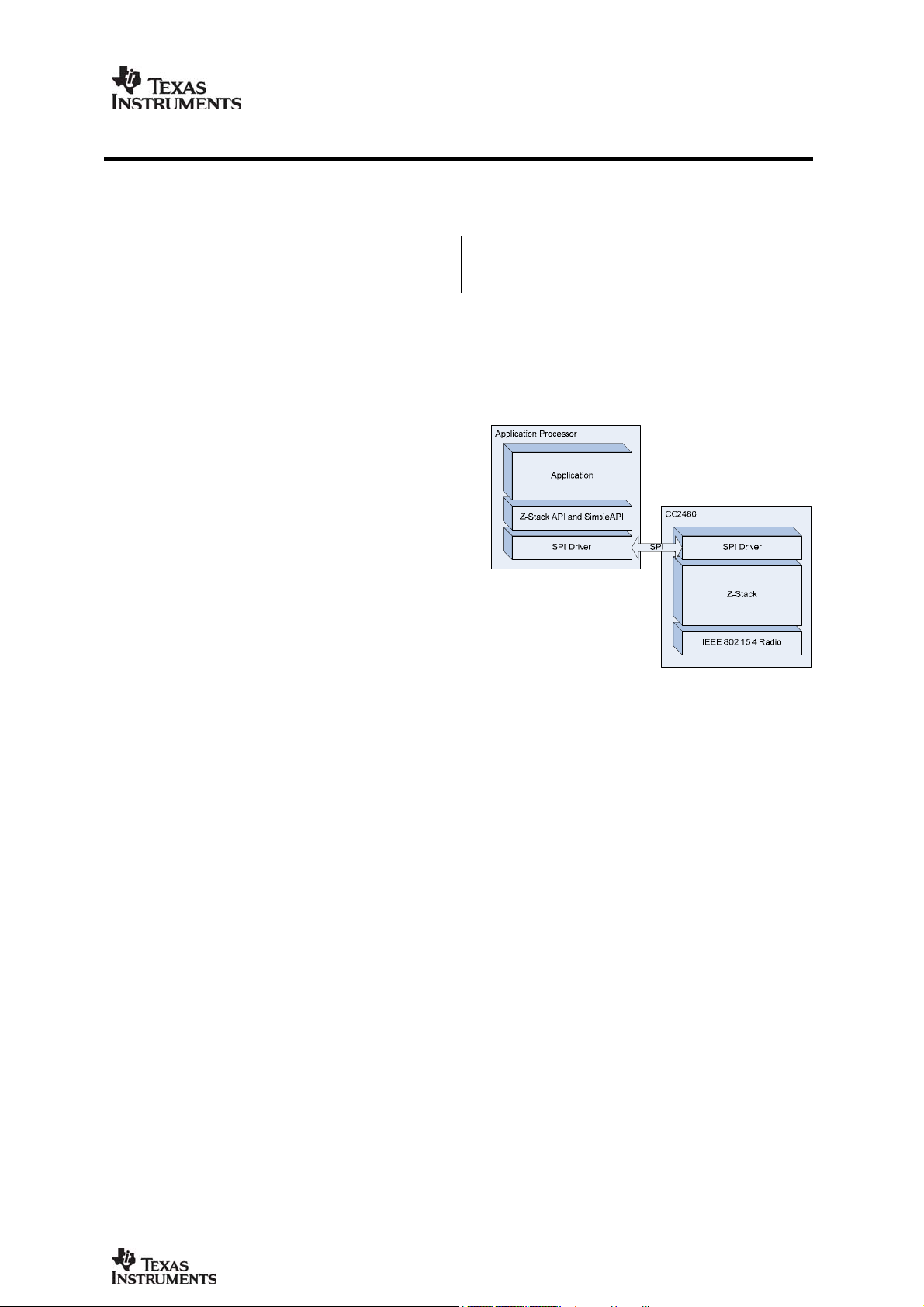
The
CC2480
is a cost-effective, low power, Z-Accel ZigBee
Processor that provides full ZigBee
functionality with a minimal development effort.
Z-Accel is a solution where TI’s ZigBee stack,
Z-Stack, runs on a ZigBee Processor and the
application runs on an external microcontroller.
CC2480
The
processing intensive ZigBee protocol tasks,
and leaves the resources of the application
microcontroller free to handle the application.
Z-Accel makes it easy to add ZigBee to new or
existing products at the same time as it
provides great flexibility in choice of
microcontroller.
CC2480
an SPI or UART interface. There is no need to
learn a new microcontroller or new tools.
CC2480
MSP430.
(formerly known as CCZACC06)
handles all the timing critical and
interfaces any microcontroller through
can for example be combined with an
• Low power wireless sensor networks
• Set-top boxes and remote controls
• Automated Meter Reading
CC2480
has only 10 API calls to learn, which drastically
simplifies the development of ZigBee
applications.
supports TI’s SimpleAPI. SimpleAPI
Key Features
• Simple integration of ZigBee into any
design
• Running the mature and stable ZigBee
2006 compliant TI Z-Stack
• SPI or UART interface to any
microcontroller running the application
• Simple API and full ZigBee API supported
• Can implement any type of ZigBee device:
Coordinator, Router or End Device
• Automatically enters low power mode (<0.5
uA) in idle periods when configured as End
Device
• Radio
o Fully integrated and robust IEEE
802.15.4-compliant 2.4 GHz DSSS
RF transceiver
o Excellent receiver sensitivity and
best in class robustness to
interferers
• Power Supply
o Wide supply voltage range (2.0V –
3.6V)
o Low current consumption (RX: 27
mA, TX: 27 mA) and fast transition
times.
• External System
o Very few external components
o RoHS compliant 7x7mm QLP48
package
• Peripherals and Supporting Functions
o Port expander with 4 general I/O
pins, two with increased sink/source
capability
o Battery monitor and temperature
sensor
o 7-12 bits ADC with two channels
o Robust power-on-reset and brown-
out-reset circuitry
• Tools and Development
o Packet sniffer PC software
o Reference designs
CC2480 Data Sheet SWRS074A Page 1 of 43
Page 2

CC2480
Table Of Contents
APPLICATIONS..............................................................................................................................................1
DESCRIPTION ................................................................................................................................................1
KEY FEATURES.............................................................................................................................................1
TABLE OF CONTENTS.................................................................................................................................2
1 ABBREVIATIONS................................................................................................................................4
2 REFERENCES...................................................................................................................................... 5
3 ABSOLUTE MAXIMUM RATINGS..................................................................................................6
4 OPERATING CONDITIONS...............................................................................................................6
5 ELECTRICAL SPECIFICATIONS....................................................................................................7
5.1 GENERAL CHARACTERISTICS ................................................................................................................8
5.2 RF RECEIVE SECTION ...........................................................................................................................9
5.3 RF TRANSMIT SECTION......................................................................................................................... 9
5.4 32 MHZ CRYSTAL OSCILLATOR..........................................................................................................10
5.5 32.768 KHZ CRYSTAL OSCILLATOR....................................................................................................10
5.6 32 KHZ RC OSCILLATOR.....................................................................................................................11
5.7 16 MHZ RC OSCILLATOR ...................................................................................................................11
5.8 FREQUENCY SYNTHESIZER CHARACTERISTICS ...................................................................................12
5.9 ANALOG TEMPERATURE SENSOR........................................................................................................12
5.10 ADC ...................................................................................................................................................12
5.11 CONTROL AC CHARACTERISTICS........................................................................................................14
5.12 SPI AC CHARACTERISTICS .................................................................................................................15
5.13 PORT OUTPUTS AC CHARACTERISTICS...............................................................................................15
5.14 DC CHARACTERISTICS ........................................................................................................................15
6 PIN AND I/O PORT CONFIGURATION ........................................................................................17
7 CIRCUIT DESCRIPTION ................................................................................................................. 19
8 APPLICATION CIRCUIT.................................................................................................................20
8.1 INPUT / OUTPUT MATCHING................................................................................................................. 20
8.2 BIAS RESISTORS ..................................................................................................................................20
8.3 CRYSTAL.............................................................................................................................................20
8.4 VOLTAGE REGULATORS ......................................................................................................................20
8.5 POWER SUPPLY DECOUPLING AND FILTERING......................................................................................21
9 PERIPHERALS...................................................................................................................................23
9.1 RESET .................................................................................................................................................23
9.2 I/O PORTS............................................................................................................................................ 23
9.3 ADC...................................................................................................................................................25
9.4 RANDOM NUMBER GENERATOR .........................................................................................................27
9.5 USART...............................................................................................................................................28
10 RADIO..................................................................................................................................................29
10.1 IEEE 802.15.4 MODULATION FORMAT...............................................................................................30
10.2 DEMODULATOR, SYMBOL SYNCHRONIZER AND DATA DECISION .......................................................31
10.3 FRAME FORMAT..................................................................................................................................31
10.4 SYNCHRONIZATION HEADER ...............................................................................................................32
10.5 MAC PROTOCOL DATA UNIT ...............................................................................................................32
10.6 FRAME CHECK SEQUENCE ................................................................................................................... 32
10.7 LINEAR IF AND AGC SETTINGS .......................................................................................................... 33
10.8 CLEAR CHANNEL ASSESSMENT...........................................................................................................33
10.9 VCO AND PLL SELF-CALIBRATION.................................................................................................... 33
10.10 INPUT / OUTPUT MATCHING................................................................................................................33
10.11 SYSTEM CONSIDERATIONS AND GUIDELINES...................................................................................... 34
10.12 PCB LAYOUT RECOMMENDATION...................................................................................................... 35
10.13 ANTENNA CONSIDERATIONS...............................................................................................................35
CC2480 Data Sheet SWRS074A Page 2 of 43
Page 3

11 VOLTAGE REGULATORS...............................................................................................................36
11.1 VOLTAGE REGULATORS POWER-ON....................................................................................................36
12 PACKAGE DESCRIPTION (QLP 48)..............................................................................................37
12.1 RECOMMENDED PCB LAYOUT FOR PACKAGE (QLP 48)...................................................................... 38
12.2 PACKAGE THERMAL PROPERTIES......................................................................................................... 38
12.3 SOLDERING INFORMAT ION ..................................................................................................................38
12.4 TRAY SPECIFICATION ..........................................................................................................................38
12.5 CARRIER TAPE AND REEL SPECIFICA TION............................................................................................ 38
13 ORDERING INFORMATION...........................................................................................................40
14 GENERAL INFORMATION.............................................................................................................41
14.1 DOCUMENT HISTORY ..........................................................................................................................41
15 ADDRESS INFORMATION.............................................................................................................. 41
16 TI WORLDWIDE TECHNICAL SUPPORT...................................................................................41
CC2480
CC2480 Data Sheet SWRS074A Page 3 of 43
Page 4

1 Abbreviations
ADC Analog to Digital Converter
AES Advanced Encryption Standard
AGC Automatic Gain Control
API Application Programming Interface
ARIB Association of Radio Industries and
Businesses
BOD Brown Out Detector
BOM Bill of Materials
CCA Clear Channel Assessment
CFR Code of Federal Regulations
CPU Central Processing Unit
CRC Cyclic Redundancy Check
CSMA-CA Carrier Sense Multiple Access with
Collision Avoidance
CW Continuous Wave
DAC Digital to Analog Converter
DC Direct Current
DNL Differential Nonlinearity
DSM Delta Sigma Modulator
DSSS Direct Sequence Spread Spectrum
EM Evaluation Module
ENOB Effective Number of bits
ESD Electro Static Discharge
ESR Equivalent Series Resistance
ETSI European Telecommunications
Standards Institute
EVM Error Vector Magnitude
FCC Federal Communications Commission
FCF Frame Control Field
FCS Frame Check Sequence
I/O Input / Output
I/Q In-phase / Quadrature-phase
IEEE Institute of Electrical and Electronics
Engineers
IF Intermediate Frequency
INL Integral Nonlinearity
ISM Industrial, Scientific and Medical
JEDEC Joint Electron Device Engineering
Council
KB 1024 bytes
kbps kilo bits per second
LFSR Linear Feedback Shift Register
LNA Low-Noise Amplifier
LO Local Oscillator
LQI Link Quality Indication
LSB Least Significant Bit / Byte
CC2480
LSB Least Significant Byte
MAC Medium Access Control
MISO Master In Slave Out
MOSI Master Out Slave In
MPDU MAC Protocol Data Unit
MSB Most Significant Byte
MUX Multiplexer
NA Not Available
NC Not Connected
O-QPSK Offset - Quadrature Phase Shift Keying
PA Power Amplifier
PCB Printed Circuit Board
PER Packet Error Rate
PHY Physical Layer
PLL Phase Locked Loop
PM{0-3} Power Mode 0-3
POR Power On Reset
PWM Pulse Width Modulator
QLP Quad Leadless Package
RAM Random Access Memory
RC Resistor-Capacitor
RCOSC RC Oscillator
RF Radio Frequency
RoHS Restriction on Hazardous Substances
RSSI Receive Signal Strength Indicator
RX Receive
SCK Serial Clock
SFD Start of Frame Delimiter
SHR Synchronization Header
SINAD Signal-to-noise and distortion ratio
SPI Serial Peripheral Interface
SRAM Static Random Access Memory
ST Sleep Timer
T/R Tape and reel
T/R Transmit / Receive
TBD To Be Decided / To Be Defined
THD Total Harmonic Distortion
TI Texas Instruments
TX Transmit
UART Universal Asynchronous
USART Universal Synchronous/Asynchronous
VGA Variable Gain Amplifier
XOSC Crystal Oscillator
Receiver/Transmitter
Receiver/Transmitter
CC2480 Data Sheet SWRS074A Page 4 of 43
Page 5

2 References
IEEE std. 802.15.4 - 2006: Wireless Medium Access Control (MAC) and Physical Layer (PHY)
[1]
specifications for Low Rate Wireless Personal Area Networks (LR-WPANs).
http://standards.ieee.org/getieee802/download/802.15.4-2006.pdf
CC2480 Interface Specification
[2]
http://www.ti.com/lit/pdf/swra175
CC2480
CC2480 Data Sheet SWRS074A Page 5 of 43
Page 6
CC2480
3 Absolute Maximum Ratings
Under no circumstances must the absolute maximum ratings given in Table 1 be violated. Stress
exceeding one or more of the limiting values may cause permanent damage to the device.
Table 1: Absolute Maximum Rati ngs
Parameter Min Max Units Condition
Supply voltage, VDD –0.3 3.9 V All supply pins must have the same voltage
Voltage on any digital pin –0.3 VDD+0.3,
Voltage on the 1.8V pins (pin no.
22, 25-40 and 42)
Input RF level 10 dBm
Storage temperature range –50 150
Reflow soldering temperature 260
ESD
–0.3 2.0 V
max 3.9
<500 V
700 V
200 V
V
Device not programmed
°C
According to IPC/JEDEC J-STD-020C
°C
On RF pads (RF_P, RF_N, AVDD_RF1,
and AVDD_RF2), according to Human
Body Model, JEDEC STD 22, method A114
All other pads, according to Human Body
Model, JEDEC STD 22, method A114
According to Charged Device Model,
JEDEC STD 22, method C101
Caution! ESD sensitive device. Precaution should be used
when handling the device in order to prevent
permanent damage.
4 Operating Conditions
The operating conditions for
Parameter Min Max Unit Condition
Operating ambient temperature
range, T
Operating supply voltage 2.0 3.6 V The supply pins to the radio part must be driven
A
CC2480
are listed in Table 2.
Table 2: Operating Conditi ons
-40 85
°C
by the 1.8 V on-chip regulator
CC2480 Data Sheet SWRS074A Page 6 of 43
Page 7
5 Electrical Specifications
CC2480
Measured on Texas Instruments
CC2480
EM reference design with TA=25°C and VDD=3.0V
unless stated otherwise.
Table 3: Electrical Specifications
Parameter Min Typ Max Unit Condition
Current Consumption
CPU Active Mode, 16 MHz,
low CPU activity
CPU Active Mode, 16 MHz,
medium CPU activity
CPU Active Mode, 16 MHz,
high CPU activity
CPU Active Mode, 32 MHz,
low CPU activity
CPU Active Mode, 32 MHz,
medium CPU activity
CPU Active Mode, 32 MHz,
high CPU activity
CPU Active and RX Mode 26.7 mA
CPU Active and TX Mode, 0dBm 26.9 mA
Power mode 1 190
Power mode 2 0.5
Power mode 3 0.3
Peripheral Current
Consumption
Sleep Timer 0.2
ADC 1.2 mA
Flash write 3 mA
Flash erase 3 mA
4.3 mA
5.1 mA
5.7 mA
9.5 mA
10.5 mA
12.3 mA
Digital regulator on. 16 MHz RCOSC running. No radio,
crystals, or peripherals active.
Low CPU activity: no flash access (i.e. only cache hit), no
RAM access.
Digital regulator on. 16 MHz RCOSC running. No radio,
crystals, or peripherals active.
Medium CPU activity: normal flash access
access.
Digital regulator on. 16 MHz RCOSC running. No radio,
crystals, or peripherals active.
High CPU activity: normal flash access, extensive RAM
access and heavy CPU load.
32 MHz XOSC running. No radio or peripherals active.
Low CPU activity : no flash access (i.e. only cache hit),
no RAM access
32 MHz XOSC running. No radio or peripherals active.
Medium CPU activity: normal flash access
access.
32 MHz XOSC running. No radio or peripherals active.
High CPU activity: normal flash access
access and heavy CPU load.
CPU running at full speed (32MHz), 32MHz XOSC
running, radio in RX mode, -50 dBm input power. No
peripherals active. Low CPU activity.
CPU running at full speed (32MHz), 32MHz XOSC
running, radio in TX mode, 0dBm output power. No
peripherals active. Low CPU activity.
Digital regulator on, 16 MHz RCOSC and 32 MHz crystal
µA
oscillator off. 32.768 kHz XOSC, POR and ST active.
RAM retention.
Digital regulator off, 16 MHz RCOSC and 32 MHz crystal
µA
oscillator off. 32.768 kHz XOSC, POR and ST active.
RAM retention.
No clocks. RAM retention. POR active.
µA
Adds to the figures above if the peripheral unit is
activated
Including 32.753 kHz RCOSC.
µA
When converting.
Estimated value
Estimated value
1
, minor RAM
1
, minor RAM
1
, extensive RAM
1
Normal Flash access means that the code used exceeds the cache storage so cache misses will
happen frequently.
CC2480 Data Sheet SWRS074A Page 7 of 43
Page 8
5.1 General Characteristics
CC2480
Measured on Texas Instruments
CC2480
EM reference design with TA=25°C and VDD=3.0V
unless stated otherwise.
Table 4: General Characteristics
Parameter Min Typ Max Unit Condition/Note
Wake-Up and Timing
Power mode 1 Æ power
mode 0
Power mode 2 or 3 Æ power
mode 0
Active Æ TX or RX
32MHz XOSC initially OFF.
Voltage regulator initially OFF
Active Æ TX or RX
Voltage regulator initially OFF
Active Æ RX or TX 192
RX/TX turnaround 192
Radio part
RF Frequency Range 2400 2483.5 MHz Programmable in 1 MHz steps, 5 MHz
Radio bit rate 250 kbps As defined by [1]
4.1
120
525
320
µs
µs
µs
µs
µs
µs
Digital regulator on, 16 MHz RCOSC and
32 MHz crystal oscillator off. Start-up of
16 MHz RCOSC.
Digital regulator off, 16 MHz RCOSC and
32 MHz crystal oscillator off. Start-up of
regulator and 16 MHz RCOSC.
Time from enabling radio part in power
mode 0, until TX or RX starts. Includes
start-up of voltage regulator and crystal
oscillator in parallel. Crystal ESR=16Ω.
Time from enabling radio part in power
mode 0, until TX or RX starts. Includes
start-up of voltage regulator.
Radio part already enabled.
Time until RX or TX starts.
between channels for compliance with
[1]
Radio chip rate
2.0 MChip/s As defined by [1]
CC2480 Data Sheet SWRS074A Page 8 of 43
Page 9
5.2 RF Receive Section
CC2480
Measured on Texas Instruments
CC2480
EM reference design with TA=25°C and VDD=3.0V
unless stated otherwise.
Table 5: RF Receive Parameters
Parameter Min Typ Max Unit Condition/Note
Receiver sensitivity
Saturation (maximum input
level)
Adjacent channel rejection
+ 5 MHz channel spacing
Adjacent channel rejection
- 5 MHz channel spacing
Alternate channel rejection
+ 10 MHz channel spacing
Alternate channel rejection
- 10 MHz channel spacing
Channel rejection
≥ + 15 MHz
≤ - 15 MHz
Co-channel rejection
Blocking / Desensitization
+ 5 MHz from band edge
+ 10 MHz from band edge
+ 20 MHz from band edge
+ 50 MHz from band edge
- 5 MHz from band edge
- 10 MHz from band edge
- 20 MHz from band edge
- 50 MHz from band edge
Spurious emission
30 – 1000 MHz
1 – 12.75 GHz
Frequency error tolerance ±140 ppm Difference between centre frequency of the received
Symbol rate error tolerance ±900 ppm Difference between incoming symbol rate and the
-92 dBm PER = 1%, as specified by [1]
Measured in 50 Ω single endedly through a balun.
[1] requires –85 dBm
10 dBm PER = 1%, as specified by [1]
Measured in 50 Ω single endedly through a balun.
[1] requires –20 dBm
41
30
55
53
55
53
-6 dB
-42
-29
-26
-22
-31
-36
-24
-25
−64
−75
Wanted signal -88dBm, adjacent modulated channel
at +5 MHz, PER = 1 %, as specified by [1].
dB
[1] requires 0 dB
Wanted signal -88dBm, adjacent modulated channel
at -5 MHz, PER = 1 %, as specified by [1].
dB
[1] requires 0 dB
Wanted signal -88dBm, adjacent modulated channel
at +10 MHz, PER = 1 %, as specified by [1]
dB
[1] requires 30 dB
Wanted signal -88dBm, adjacent modulated channel
at -10 MHz, PER = 1 %, as specified by [1]
dB
[1] requires 30 dB
Wanted signal @ -82 dBm. Undesired signal is an
802.15.4 modulated channel, stepped through all
dB
channels from 2405 to 2480 MHz. Signal level for
dB
PER = 1%. Values are estimated.
Wanted signal @ -82 dBm. Undesired signal is
802.15.4 modulated at the same frequency as the
desired signal. Signal level for PER = 1%.
dBm
Wanted signal 3 dB above the sensitivity level, CW
dBm
jammer, PER = 1%. Measured according to EN 300
dBm
440 class 2.
dBm
dBm
dBm
dBm
dBm
dBm
Conducted measurement in a 50 Ω single ended
dBm
load. Complies with EN 300 328, EN 300 440 class
2, FCC CFR47, Part 15 and ARIB STD-T-66.
RF signal and local oscillator frequency.
[1] requires minimum 80 ppm
internally generated symbol rate
[1] requires minimum 80 ppm
5.3 RF Transmit Section
Measured on Texas Instruments
CC2480
EM reference design with TA=25°C, VDD=3.0V, and
nominal output power unless stated otherwise.
CC2480 Data Sheet SWRS074A Page 9 of 43
Page 10
Table 6: RF Transmit Parameters
Parameter Min Typ Max Unit Condition/Note
Nominal output
power
Harmonics
nd
2
harmonic
rd
3
harmonic
th
4
harmonic
th
5
harmonic
Spurious emission
30 - 1000 MHz
1– 12.75 GHz
1.8 – 1.9 GHz
5.15 – 5.3 GHz
EVM 11 % Measured as defined by [1]
Optimum load
impedance
0 dBm
-50.7
-55.8
-54.2
-53.4
-47
-43
-58
-56
60
+ j164
Delivered to a single ended 50 Ω load through a balun.
[1] requires minimum –3 dBm
Measurement conducted with 100 kHz resolution bandwidth on
dBm
spectrum analyzer. Output Delivered to a single ended 50 Ω load
dBm
through a balun.
dBm
dBm
Maximum output power.
Texas Instruments
dBm
EN 300 328, EN 300 440, FCC CFR47 Part 15 and ARIB STD-
dBm
T-66.
Transmit on 2480MHz under FCC is supported by duty-cycling
dBm
The peak conducted spurious emission is -47 dBm @ 192 MHz
dBm
which is in an EN 300 440 restricted band limited to -54 dBm. All
radiated spurious emissions are within the limits of
ETSI/FCC/ARIB. Conducted spurious emission (CSE) can be
reduced with a simple band pass filter connected between
matching network and RF connector (1.8 pF in parallel with 1.6
nH reduces the CSE by 20 dB), this filter must be connected to
good RF ground.
[1] requires max. 35 %
Ω
Differential impedance as seen from the RF-port (
RF_N) towards the antenna
CC2480
CC2480
EM reference design complies with
2
.
RF_P and
5.4 32 MHz Crystal Oscillator
Measured on Texas Instruments
CC2480
EM reference design with TA=25°C and VDD=3.0V
unless stated otherwise.
Table 7: 32 MHz Crystal Oscillator Parameters
Parameter Min Typ Max Unit Condition/Note
Crystal frequency 32 MHz
Crystal frequency
accuracy
requirement
ESR 6 16 60
C0 1 1.9 7 pF Simulated over operating conditions
CL 10 13 16 pF Simulated over operating conditions
Start-up time 212 µs
- 40 40 ppm Including aging and temperature dependency, as specified by [1]
Simulated over operating conditions
Ω
5.5 32.768 kHz Crystal Oscillator
Measured on Texas Instruments
CC2480
EM reference design with TA=25°C and VDD=3.0V
unless stated otherwise.
2
This is for 2440MHz
CC2480 Data Sheet SWRS074A Page 10 of 43
Page 11
Table 8: 32.768 kHz Crystal Oscillator Parameters
Parameter Min Typ Max Unit Condition/Note
Crystal frequency 32.768 kHz
Crystal frequency
accuracy
requirement
ESR 40 130
C0 0.9 2.0 pF Simulated over operating conditions
CL 12 16 pF Simulated over operating conditions
Start-up time 400 ms Value is simulated.
5.6 32 kHz RC Oscillator
–40 40 ppm Including aging and temperature dependency, as specified by [1]
Simulated over operating conditions
kΩ
CC2480
Measured on Texas Instruments
CC2480
EM reference design with TA=25°C and VDD=3.0V
unless stated otherwise.
Table 9: 32 kHz RC Oscillator parameters
Parameter Min Typ Max Unit Condition/Note
Calibrated frequency 32.753 kHz The calibrated 32 kHz RC Oscillator frequency
Frequency accuracy after
calibration
Temperature coefficient +0.4
Supply voltage coefficient +3 % / V Frequency drift when supply voltage changes
Initial calibration time 1.7 ms
±0.2 % Value is estimated.
% / °C
is the 32 MHz XTAL frequency divided by 977
Frequency drift when temperature changes
after calibration. Value is estimated.
after calibration. Value is estimated.
When the 32 kHz RC Oscillator is enabled,
calibration is continuously done in the
background as long as the 32 MHz crystal
oscillator is running.
5.7 16 MHz RC Oscillator
Measured on Texas Instruments
CC2480
EM reference design with TA=25°C and VDD=3.0V
unless stated otherwise.
Table 10: 16 MHz RC Oscillator parameters
Parameter Min Typ Max Unit Condition/Note
Frequency 16 MHz The calibrated 16 MHz RC Oscillator
Uncalibrated frequency
accuracy
Calibrated frequency
accuracy
Start-up time 10 µs
Temperature coefficient -325
Supply voltage coefficient 28
Initial calibration time 50 µs When the 16 MHz RC Oscillator is enabled it
±18
±0.6 ±1
%
%
ppm / °C
ppm / mV
frequency is the 32 MHz XTAL frequency
divided by 2
Frequency drift when temperature changes
after calibration
Frequency drift when supply voltage changes
after calibration
will be calibrated continuously when the
32MHz crystal oscillator is running.
CC2480 Data Sheet SWRS074A Page 11 of 43
Page 12
5.8 Frequency Synthesizer Characteristics
CC2480
Measured on Texas Instruments
CC2480
EM reference design with TA=25°C and VDD=3.0V
unless stated otherwise.
Table 11: Frequency Synthesizer Parameters
Parameter Min Typ Max Unit Condition/Note
Phase noise
−116
−117
−118
PLL lock time
192
dBc/Hz
dBc/Hz
dBc/Hz
µs
Unmodulated carrier
At ±1.5 MHz offset from carrier
At ±3 MHz offset from carrier
At ±5 MHz offset from carrier
The startup time until RX/TX turnaround. The crystal
oscillator is running.
5.9 Analog Temperature Sensor
Measured on Texas Instruments
CC2480
EM reference design with TA=25°C and VDD=3.0V
unless stated otherwise.
Table 12: Analog Temperature Sensor Parameters
Parameter Min Typ Max Unit Condition/Note
Output voltage at –40°C
Output voltage at 0°C
Output voltage at +40°C
Output voltage at +80°C
Temperature coefficient 2.45
Absolute error in calculated
temperature
Error in calculated
temperature, calibrated
Current consumption
increase when enabled
0.648 V Value is estimated
0.743 V Value is estimated
0.840 V Value is estimated
0.939 V Value is estimated
mV/°C Fitted from –20°C to +80°C on estimated values.
–8
-2 0 2
280 µA
°C From –20°C to +80°C when assuming best fit for
absolute accuracy on estimated values: 0.743V at
0°C and 2.45mV / °C.
°C From –20°C to +80°C when using 2.45mV / °C,
after 1-point calibration at room temperature.
Values are estimated. Indicated min/max with 1point calibration is based on simulated values for
typical process parameters
5.10 ADC
Measured with T
Instruments’
=25°C and VDD=3.0V. Note that other data may result when using Texas
A
CC2480
EM reference design.
Table 13: ADC Characteristics
Parameter Min Typ Max Unit Condition/Note
Input voltage 0 VDD V VDD is voltage on AVDD_SOC pin
Input resistance, signal 197 kΩ Simulated using 4 MHz clock speed.
Full-Scale Signal3 2.97 V Peak-to-peak, defines 0dBFS
3
Measured with 300 Hz Sine input and VDD as reference.
CC2480 Data Sheet SWRS074A Page 12 of 43
Page 13
CC2480
Parameter Min Typ Max Unit Condition/Note
ENOB3 5.7 bits 7-bits setting.
Single ended input 7.5 9-bits setting.
9.3 10-bits setting.
10.8 12-bits setting.
Error! Bookmark not defined.
ENOB
Differential input 8.3 9-bits setting.
10.0 10-bits setting.
11.5 12-bits setting.
Useful Power Bandwidth 0-20 kHz 7-bits setting
THD3
-Single ended input -75.2 dB 12-bits setting, -6dBFS
-Differential input -86.6 dB 12-bits setting, -6dBFS
Signal To Non-Harmonic Ratio3
-Single ended input 70.2 dB 12-bits setting
-Differential input 79.3 dB 12-bits setting
Spurious Free Dynamic Range3
-Single ended input 78.8 dB 12-bits setting, -6dBFS
-Differential input 88.9 dB 12-bits setting, -6dBFS
CMRR, differential input <-84 dB 12- bit setting, 1 kHz Sine (0dBFS), limited by ADC
Crosstalk, single ended input <-84 dB 12- bit setting, 1 kHz Sine (0dBFS), limited by ADC
Offset -3 mV Mid. Scale
Gain error 0.68 %
DNL3 0.05 LSB 12-bits setting, mean
0.9 LSB 12-bits setting, max
INL3 4.6 LSB 12-bits setting, mean
13.3 LSB 12-bits setting, max
SINAD3 35.4 dB 7-bits setting.
Single ended input 46.8 dB 9-bits setting.
(-THD+N) 57.5 dB 10-bits setting.
66.6 dB 12-bits setting.
Error! Bookmark not defined.
SINAD
Differential input 51.6 dB 9-bits setting.
(-THD+N) 61.8 dB 10-bits setting.
70.8 dB 12-bits setting.
Conversion time 20
36
68
132
Power Consumption 1.2 mA
6.5 bits 7-bits setting.
resolution
resolution
40.7 dB 7-bits setting.
7-bits setting.
µs
9-bits setting.
µs
10-bits setting.
µs
12-bits setting.
µs
CC2480 Data Sheet SWRS074A Page 13 of 43
Page 14
5.11 Control AC Characteristics
= -40°C to 85°C, VDD=2.0V to 3.6V if nothing else stated.
T
A
Table 14: Control Inputs AC Characteristics
Parameter Min Typ Max Unit Condition/Note
CC2480
System clock,
f
SYSCLK
t
= 1/ f
SYSCLK
RESET_N low
width
Interrupt pulse
width
SYSCLK
16 32 MHz System clock is 32 MHz when crystal oscillator is used.
250 ns See item 1, Figure 1. This is the shortest pulse that is
t
ns See item 2, Figure 1.This is the shortest pulse that is
SYSCLK
RESET_N
GPIOx
GPIOx
System clock is 16 MHz when calibrated 16 MHz RC
oscillator is used.
guaranteed to be recognized as a complete reset pin
request. Note that shorter pulses may be recognized but
will not lead to complete reset of all modules within the
chip.
guaranteed to be recognized as an interrupt request. In
PM2/3 the internal synchronizers are bypassed so this
requirement does not apply in PM2/3.
1
2
2
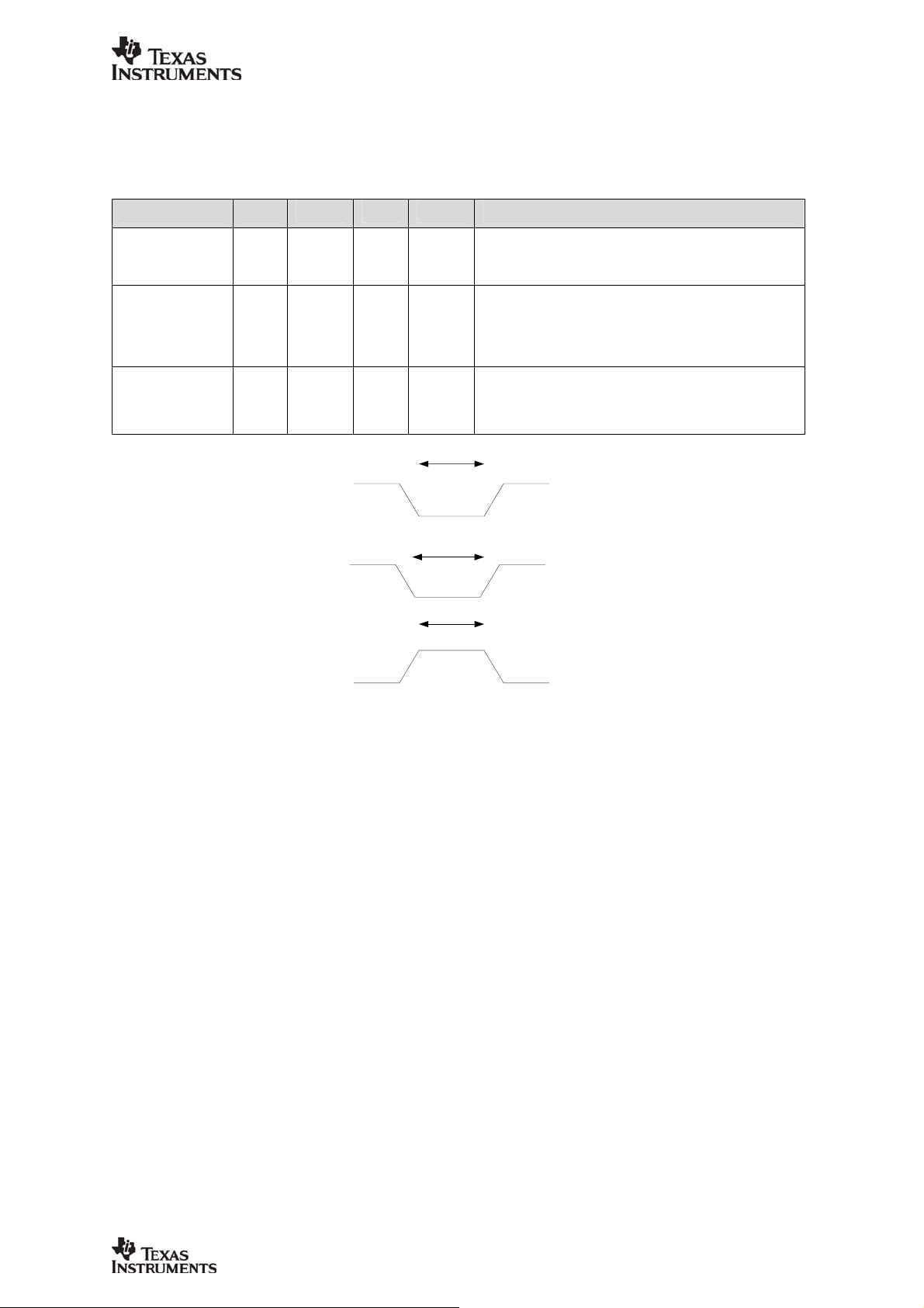
Figure 1: Control Inputs AC Characteristics
CC2480 Data Sheet SWRS074A Page 14 of 43
Page 15

5.12 SPI AC Characteristics
= -40°C to 85°C, VDD=2.0V to 3.6V if nothing else stated.
T
A
Table 15: SPI AC Characteristics
Parameter Min Typ Max Unit Condition/Note
CC2480
SSN low to SCK 2*t
SCK to SSN high 30 ns See item 6 Figure 2
SCK period 100 ns See item 1 Figure 2
SCK duty cycle 50%
SI setup 10 ns See item 2 Figure 2
SI hold 10 ns See item 3 Figure 2
SCK to SO 25 ns See item 4 Figure 2, load = 10 pF
See item 5 Figure 2
SYSCLK
Figure 2: SPI AC Characteristics
5.13 Port Outputs AC Characteristics
= 25°C, VDD=3.0V if nothing else stated.
T
A
Table 16: Port Outputs AC Characteristics
Parameter Min Typ Max Unit Condition/Note
GPIO/USART output
rise time
(SC=0/SC=1)
fall time
(SC=0/SC=1)
3.15/
1.34
3.2/
1.44
ns
Load = 10 pF
Timing is with respect to 10% VDD and 90% VDD levels.
Values are estimated
Load = 10 pF
Timing is with respect to 90% VDD and 10% VDD.
Values are estimated
5.14 DC Characteristics
The DC Characteristics of
=25°C, VDD=3.0V if nothing else stated.
T
A
CC2480
are listed in Table 17 below.
Table 17: DC Characteristics
CC2480 Data Sheet SWRS074A Page 15 of 43
Page 16

Digital Inputs/Outputs Min Typ Max Unit Condition
Logic "0" input voltage 30 % Of VDD supply (2.0 – 3.6 V)
Logic "1" input voltage 70 % Of VDD supply (2.0 – 3.6 V)
Logic "0" input current per pin NA 12 nA Input equals 0V
Logic "1" input current NA 12 nA Input equals VDD
Total logic “0” input current all pins 70 nA
Total logic “1” input current all pins 70 nA
I/O pin pull-up and pull-down
resistor
20 kΩ
CC2480
CC2480 Data Sheet SWRS074A Page 16 of 43
Page 17
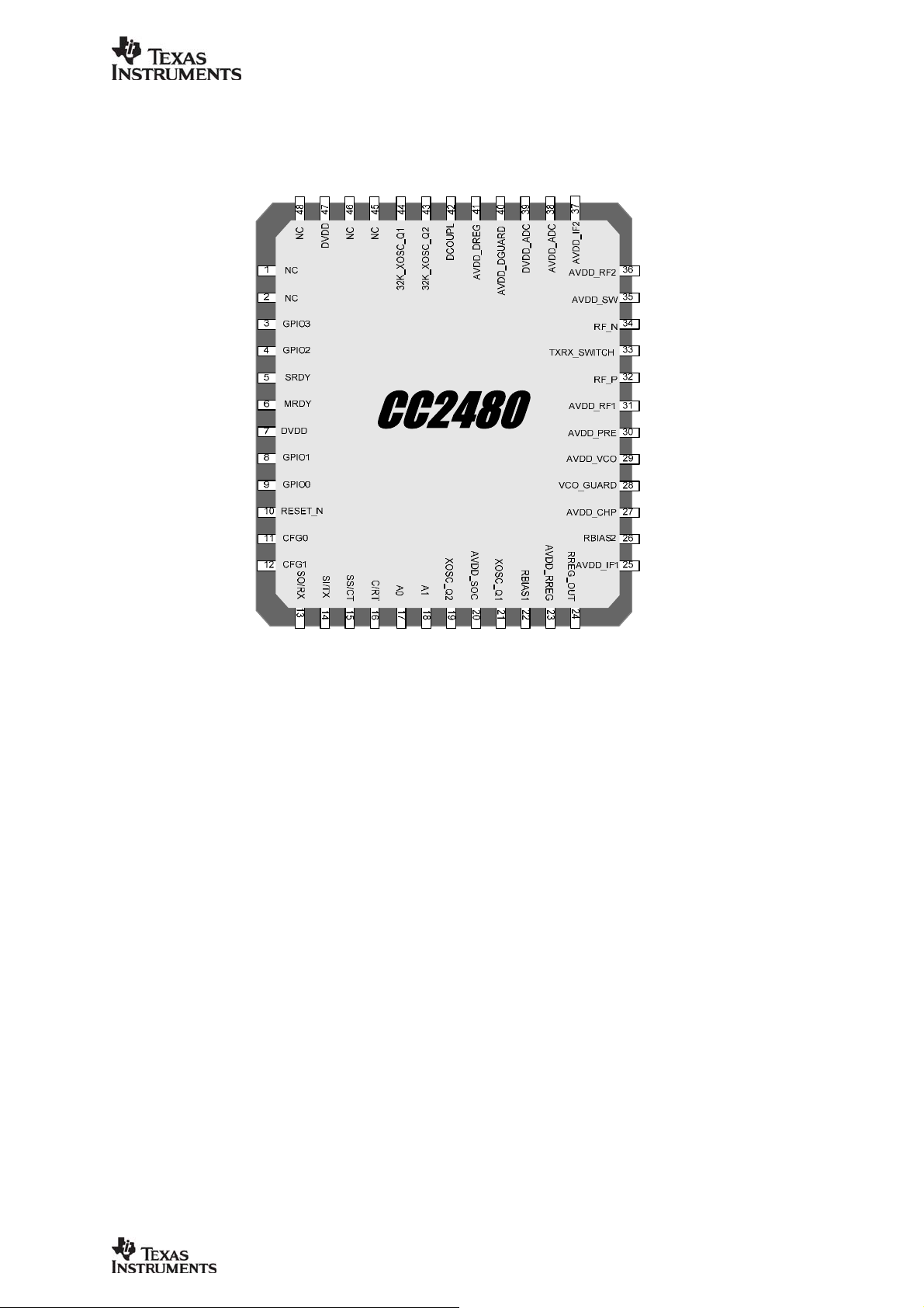
6 Pin and I/O Port Configuration
The
CC2480
pinout is shown in Figure 3 with details in Table 18.
CC2480
Figure 3: Pinout top view
Note: The exposed die attach pad must be connected to a solid ground plane as this is the
ground connection for the chip.
CC2480 Data Sheet SWRS074A Page 17 of 43
Page 18

CC2480
Table 18: Pinout overview
Pin Pin name Pin type Description
- GND Ground The exposed die attach pad must be connected to a solid ground plane
1 NC N/A
2 NC N/A
3 GPIO3 Digital I/O General I/O pin 3
4 GPIO2 Digital I/O General I/O pin 2
5 SRDY Digital Output Slave ready. Mandatory for SPI, optional for UART.
6 MRDY Digital Input Master ready. Optional for SPI and UART.
7 DVDD Power (Digital) 2.0V-3.6V digital power supply for digital I/O
8 GPIO1 Digital I/O General I/O pin 1 – increased drive capability
9 GPIO0 Digital I/O General I/Opin 0 – increased drive capability
10 RESET_N Digital input Reset, active low
11 CFG0 Digital Input Configuration input 0
12 CFG1 Digital Input Configuration input 1
13 SO/RX Digital Input SPI slave output or UART RX data
14 SI/TX Digital Output SPI slave input or UART TX data
15 SS/CT Digital I/O SPI slave select (in) or UART CTS (out)
16 C/RT Digital Input SPI clock or UART RTS
17 A0 Analog Input ADC input A0
18 A1 Analog Input ADC input A1
19 XOSC_Q2 Analog I/O 32 MHz crystal oscillator pin 2
20 AVDD_SOC Power (Analog) 2.0V-3.6V analog power supply connection
21 XOSC_Q1 Analog I/O 32 MHz crystal oscillator pin 1, or external clock input
22 RBIAS1 Analog I/O External precision bias resistor for reference current
23 AVDD_RREG Power (Analog) 2.0V-3.6V analog power supply connection
24 RREG_OUT Power output 1.8V Voltage regulator power supply output. Only intended for supplying the analog
25 AVDD_IF1 Power (Analog) 1.8V Power supply for the receiver band pass filter, analog test module, global bias
26 RBIAS2 Analog output
27 AVDD_CHP Power (Analog) 1.8V Power supply for phase detector, charge pump and first part of loop filter
28 VCO_GUARD Power (Analog) Connection of guard ring for VCO (to AVDD) shielding
29 AVDD_VCO Power (Analog) 1.8V Power supply for VCO and last part of PLL loop filter
30 AVDD_PRE Power (Analog) 1.8V Power supply for Prescaler, Div-2 and LO buffers
31 AVDD_RF1 Power (Analog) 1.8V Power supply for LNA, front-end bias and PA
32 RF_P RF I/O Positive RF input signal to LNA during RX. Positive RF output signal from PA during
33 TXRX_SWITCH Power (Analog) Regulated supply voltage for PA
34 RF_N RF I/O Negative RF input signal to LNA during RX
35 AVDD_SW Power (Analog) 1.8V Power supply for LNA / PA switch
36 AVDD_RF2 Power (Analog) 1.8V Power supply for receive and transmit mixers
37 AVDD_IF2 Power (Analog) 1.8V Power supply for transmit low pass filter and last stages of VGA
38 AVDD_ADC Power (Analog) 1.8V Power supply for analog parts of ADCs and DACs
39 DVDD_ADC Power (Digital) 1.8V Power supply for digital parts of ADCs
40 AVDD_DGUARD Power (Digital) Power supply connection for digital noise isolation
41 AVDD_DREG Power (Digital) 2.0V-3.6V digital power supply for digital core voltage regulator
42 DCOUPL Power (Digital) 1.8V digital power supply decoupling. Do not use for supplying external circuits.
43 32K_XOSC_Q2 Analog I/O 32.768 kHz XOSC
44 32K_XOSC_Q1 Analog I/O 32.768 kHz XOSC
45 NC N/A
46 NC N/A
47 DVDD Power (Digital) 2.0V-3.6V digital power supply for digital I/O
48 NC N/A
1.8V part (power supply for pins 25, 27-31, 35-40).
and first part of the VGA
External precision resistor, 43 kΩ, ±1 %
TX
Negative RF output signal from PA during TX
CC2480 Data Sheet SWRS074A Page 18 of 43
Page 19

7 Circuit Description
DIGITAL
ANALOG
MIXED
32K_XOSC_Q2
32K_XOSC_Q1
32 MHz
CRYSTAL OSC
HIGH SPEED
RC-OSC
ON-CHIP VOLTAGE
REGULATOR
POWER ON RESET
BROWN OUT
VDD (2.0 - 3.6 V)
DCOUPL
CC2480
XOSC_Q2
XOSC_Q1
GPIO3
GPIO2
GPIO1
GPIO0
SRDY
MRDY
SI/TX
SO/RX
SS/CT
C/RT
32.768 kHz
CRYSTAL OSC
RESETRESET_N
GP
DMA
I/O
A1
A0
∆Σ ADC
AUDIO / DC
2 CHANNELS
32 kHz RC-OSC
CLOCK MUX &
CALIBRATION
ENCRYPTION
DECRYPTION
USART
8051 CPU
CORE
AES
&
SLEEP TIMER
SLEEP MODE CONTROLLER
MEMORY
ARBITRATOR
IRQ
CTRL
DEMODULATOR
RECEIVE
CHAIN
AGC
FREQUENCY
128 KB
FLASH
8 KB
SRAM
FLASH
WRITE
MODULATOR
TRANSMIT
SYNTHESIZER
IEEE 802.15.4 MAC TIMER
CHAIN
FIFO AND FRAME CONTROL
Figure 4: CC2480 Block Diagram
A block diagram of
CC2480
4. The modules can be rough
one of three categori d modules,
es: CPU-relate
own in Figure
is sh
ly divided into features an
modules related to power and clock
RF_P RF_N
distribution, and radio-related modules.
IEEE 802.15.4 compliant radio
based on the leading
CC2420
transceive
Section 10 for details.
CC2480
r. See
CC2480 Data Sheet SWRS074A Page 19 of 43
Page 20

8 Application Circuit
CC2480
Few external components are required for the
operation of
circuit is shown in Figure 5. Typical values and
8.1 Input / output matching
The RF input/output is high impedance and
differential. The optimum differential load for
the RF port is 60 + j164 Ω
When using an unbalanced antenna such as a
monopole, a balun should be used in order to
optimize performance. The balun can be
implemented using low-cost discrete inductors
and capacitors. The recommended balun
shown, consists of C341, L341, L321 and
L331 together with a PCB microstrip
transmission line (λ/2-dipole), and will match
the RF input/output to 50 Ω. An internal T/R
switch circuit is used to switch between the
4
This is for 2440MHz.
8.2 Bias resistors
The bias resistors are R221 and R261. The
bias resistor R221 is used to set an accurate
bias current for the 32 MHz crystal oscillator.
CC2480
. A typical application
4
.
description of external components are shown
in Table 19.
LNA (RX) and the PA (TX). See Input/output
matching section on page 33 for more details.
If a balanced antenna such as a folded dipole
is used, the balun can be omitted. If the
antenna also provides a DC path from
TXRX_SWITCH pin to the RF pins, inductors
are not needed for DC bias.
Figure 5 shows a suggested application circuit
using a differential antenna. The antenna type
is a standard folded dipole. The dipole has a
virtual ground point; hence bias is provided
without degradation in antenna performance.
Also refer to the section Antenna
Considerations on page 35.
8.3 Crystal
An external 32 MHz crystal, XTAL1, with two
loading capacitors (C191 and C211) is used
for the 32 MHz crystal oscillator. See page 10
for details. The load capacitance seen by the
32 MHz crystal is given by:
C +
=
1
+
CC
XTAL2 is an optional 32.768 kHz crystal, with
two loading capacitors (C441 and C431), used
for the 32.768 kHz crystal oscillator. The
32.768 kHz crystal oscillator is used in
applications where you need both very low
8.4 Voltage regulators
The on chip voltage regulators supply all 1.8 V
power supply pins and internal power supplies.
C
11
211191
parasiticL
sleep current consumption and accurate wake
up times. The load capacitance seen by the
32.768 kHz crystal is given by:
C +
=
1
+
CC
A series resistor may be used to comply with
the ESR requirement.
C241 and C421 are required for stability of the
regulators.
C
11
431441
parasiticL
CC2480 Data Sheet SWRS074A Page 20 of 43
Page 21

8.5 Power supply decoupling and filtering
CC2480
Proper power supply decoupling must be used
for optimum performance. The placement and
size of the decoupling capacitors and the
power supply filtering are very important to
achieve the best performance in an
application. TI provides a compact reference
design that should be followed very closely.
C441
optional
4847464544434241403938
NC
DVDD
1
NC
2
NC
3
GPIO3
GPIO2
4
5
SRDY
6
MRDY
7
DVDD
GPIO1
8
9
GPIO0
RESET_N
10
11
CFG0
CFG1
12
SO/RX
SI/TX
13
14
C431
C421
2.0 - 3.6V Power Supply
XTAL2
NC
NC
DCOUPL
AVDD_DREG
32K_XOSC_Q2
32K_XOSC_Q1
AVDD_DGUARD
QLP48
CC2480
7x7
AVDD_SOC
XOSC_Q2
SS/CT
C/RT
A1
A0
15
16
171819
XOSC_Q1
202122
XTAL1
C211C191
DVDD_ADC
RBIAS1
R221
37
AVDD_IF2
AVDD_ADC
AVDD_RF2
AVDD_SW
TXRX_SWITCH
AVDD_RF1
AVDD_PRE
AVDD_VCO
VCO_GUARD
AVDD_CHP
RBIAS2
AVDD_RREG
RREG_OUT
AVDD_IF1
24
23
C241
RF_N
RF_P
36
35
34
33
32
31
30
29
28
27
26
25
Refer to the section PCB Layout
Recommendation on page 35.
Figure 5:
CC2480
Applicatio
n Circuit.
(Digital I/O
and ADC
interface
not
connected
).
Antenna
(50 Ohm)
Decouplin
g
capacitors
shownot n.
L321
R261
λ/4
L331
λ/4
L331
L341
C341
or
Folded Dipole PCB
Antenna
L321
CC2480 Data Sheet SWRS074A Page 21 of 43
Page 22

Table 19: Overview of external components (excluding supply decoupling capacitors)
CC2480
Component Description
C191 32 MHz crystal load capacitor 33 pF, 5%, NP0, 0402 33 pF, 5%, NP0, 0402
C211 32 MHz crystal load capacitor 27 pF, 5%, NP0, 0402 27 pF, 5%, NP0, 0402
C241 Load capacitance for analogue power
supply voltage regulators
C421 Load capacitance for digital power supply
voltage regulators
Note: For RF connector a LP filter can be
connected between this C, the antenna
and good ground in order to remove
conducted spurious emission by using
1.8pF in parallel with 1.6nH
C431, C441 32.768 kHz crystal load capacitor (if low-
frequency crystal is needed in application)
L321 Discrete balun and match 6.8 nH, 5%,
L331 Discrete balun and match 22 nH, 5%,
L341 Discrete balun and match 1.8 nH, +/-0.3 nH,
R221 Precision resistor for current reference
generator to system-on-chip part
R261 Precision resistor for current reference
generator to RF part
XTAL1 32 MHz Crystal 32 MHz crystal,
XTAL2 Optional 32.768 kHz watch crystal (if low-
frequency crystal is needed in application)
Single Ended 50Ω Output
220 nF, 10%, 0402 220 nF, 10%, 0402
1 µF, 10%, 0402 1 µF, 10%, 0402
5.6 pF, 5%, NP0, 0402 Not used C341 DC block to antenna and match
1.8 pF, Murata COG 0402,
GRM15
1.6 nH, Murata 0402,
LQG15HS1N6S02
15 pF, 5%, NP0, 0402 15 pF, 5%, NP0, 0402
Monolithic/multilayer, 0402
Monolithic/multilayer, 0402
Monolithic/multilayer, 0402
56 kΩ, 1%, 0402 56 kΩ, 1%, 0402
43 kΩ, 1%, 0402 43 kΩ, 1%, 0402
ESR < 60 Ω
32.768 kHz crystal,
Epson MC 306.
Differential Antenna
12 nH 5%,
Monolithic/multilayer, 0402
27 nH, 5%,
Monolithic/multilayer, 0402
Not used
32 MHz crystal,
ESR < 60 Ω
32.768 kHz crystal,
Epson MC 306.
CC2480 Data Sheet SWRS074A Page 22 of 43
Page 23

9 Peripherals
In the following sub-sections the useraccessible
CC2480
described in detail.
9.1 Reset
peripheral modules are
CC2480
The
CC2480
has four reset sources. The
following events generate a reset:
• Forcing RESET_N input pin low
• A power-on reset condition
• A brown-out reset condition
• A firmware-generated reset
(SYS_RESET_REQ [2])
9.1.1 Power On Reset and Brown Out Detector
The
CC2480
includes a Power On Reset (POR)
providing correct initialization during device
power-on. Also includes is a Brown Out
Detector (BOD) operating on the regulated
1.8V digital power supply only, The BOD will
protect the memory contents during supply
voltage variations which cause the regulated
1.8V power to drop below the minimum level
required by flash memory and SRAM.
When power is initially applied to the
CC2480
the Power On Reset (POR) and Brown Out
Detector (BOD) will hold the device in reset
VOLT
1.8V REGULATED
The initial conditions after a reset are as
follows:
• I/O pins are configured as inputs with pull-
up
• See the
CC2480
Interface Specification [2]
for a description of the interaction between
CC2480 and the host processor after
reset.
state until the supply voltage reaches above
the Power On Reset and Brown Out voltages.
Figure 6 shows the POR/BOD operation with
the 1.8V (typical) regulated supply voltage
together with the active low reset signals
BOD_RESET and POR_RESET shown in the
bottom of the figure (note that signals are not
available, just for illustration of events).
UNREGULATED
BOD RESET ASSERT
POR RESET DEASSERT RISING VDD
POR RESET ASSERT FALLING VDD
0
POR OUTPUT
BOD RESET
POR RESET
Figure 6 : Power On Reset and Brown Out Detector Operation
9.2 I/O ports
The
CC2480
has digital input/output pins that
have the following key features:
X
X
X
• General purpose I/O or peripheral I/O
• Pull-up or pull-down capability on inputs
• External interrupt capability
Two of the I/O pins have external interrupts
that can be used to wake up the device from
sleep modes.
CC2480 Data Sheet SWRS074 Page 23 of 43
X
X
X
Page 24

9.2.1 Unused I/O pins
CC2480
Unused I/O pins should have a defined level
and not be left floating. One way to do this is to
leave the pin unconnected and configured with
9.2.2 Low I/O Supply Voltage
In applications where the digital I/O power
supply voltage pin DVDD is below 2.6 V, the
SC bit should be set to 1 in order to obtain
output DC characteristics specified in section
9.2.3 General Purpose I/O
See the
of how to configure and use the GPIO pins.
The output drive strength is 4 mA on all
outputs, except for the two high-drive outputs,
GPIO0 and GPIO1, which each have ~20 mA
output drive strength.
When used as an input, the general purpose
I/O port pins can be configured to have a pull-
CC2480
user guide [2] for a description
pull-up resistor. This is also the state of all pins
after reset.
5.14. See the
description of how to do this.
up, pull-down or tri-state mode of operation. By
default, after a reset, inputs are configured as
inputs with pull-up. Please note that GPIO0
and GPIO1 do not have pull-up or pull-down
capabilities.
In power modes PM2 and PM3 the I/O pins
retain the I/O mode and output value (if
applicable) that was set when PM2/3 was
entered
CC2480
user guide [2] for a
CC2480 Data Sheet SWRS074 Page 24 of 43
Page 25

9.3 ADC
9.3.1 ADC Introduction
CC2480
The ADC supports up to 12-bit analog-todigital conversion. The ADC includes an
analog multiplexer with up to two individually
configurable channels and reference voltage
generator.
The main features of the ADC are as follows:
A1
A0
VDD/3
TMP_SENSOR
Int 1.25V
input
input
mux
mux
Sigma-delta
modulator
Figure 7: ADC block diagram.
• Selectable decimation rates which also
sets the resolution (7 to 12 bits).
• Two individual input channels, singleended or differential
• Internal voltage reference
• Temperature sensor input
• Battery measurement capability
Decimation
filter
Clock generation and
control
9.3.2 ADC Operation
This section describes the general setup and
operation of the ADC.
9.3.2.1 ADC Core
The ADC includes an ADC capable of
converting an analog input into a digital
representation with up to 12 bits resolution.
9.3.2.2 ADC Inputs
The signals from input pins A0 and A1 are
used as single-ended ADC inputs. The ADC
automatically performs a sequence of
conversions when the SYS_ADC_READ
command is issued.
In addition to the input pins A0-1, the output of
an on-chip temperature sensor can be
9.3.2.3 ADC conversion sequences
The
CC2480
connected to external pins. Additionally, the
ADC can measure the chip voltage and
temperature.
The ADC conversions are done channel by
channel incrementally.
The two external pin inputs A0 and A1 can be
used as single-ended or differential inputs.
has two ADC channels that are
The ADC uses a selectable positive reference
voltage.
selected as an input to the ADC for
temperature measurements.
It is also possible to select a voltage
corresponding to AVDD_SOC/3 as an ADC
input. This input allows the implementation of
e.g. a battery monitor in applications where
this feature is required.
In the case where differential inputs are
selected, the differential inputs consist of the
input pair A0-1. Note that no negative supply
can be applied to these pins, nor a supply
larger than VDD (unregulated power). It is the
difference between the pairs that are
converted in differential mode.
CC2480 Data Sheet SWRS074 Page 25 of 43
Page 26

CC2480
In addition to the input pins A0-1, the output of
an on-chip temperature sensor can be
selected as an input to the ADC for
temperature measurements.
9.3.2.4 ADC Operating Modes
This section describes the operating modes
and initialization of conversions.
The ADC uses an internal voltage reference
for single-ended conversions.
9.3.2.5 ADC Conversion Results
The digital conversion result is represented in
two's complement form. The result is always
positive. This is because the result is the
difference between ground and input signal
which is always posivitely signed
(Vconv=Vinp-Vinn, where Vinn=0V). The
maximum value is reached when the input
amplitude is equal VREF, the internal voltage
reference.
9.3.2.6 ADC Reference Voltage
It is also possible to select a voltage
corresponding to AVDD_SOC/3 as an ADC
input. This input allows the implementation of
e.g. a battery monitor in applications where
this feature is required.
The decimation rate (and thereby also the
resolution and time required to complete a
conversion and sample rate) is configurable
from 7-12 bits.
For differential configurations the difference
between the pins is converted and this
difference can be negatively signed. For 12-bit
resolution the digital conversion result is 2047
when the analog input, Vconv, is equal to
VREF, and the conversion result is -2048
when the analog input is equal to –VREF.
The positive reference voltage for analog-todigital conversions is an internally generated
1.25V voltage.
9.3.2.7 ADC Conversion Timing
The ADC is run on the 32MHz system clock,
which is divided by 8 to give a 4 MHz clock.
The time required to perform a conversion
depends on the selected decimation rate.
When the decimation rate is set to for instance
128, the decimation filter uses exactly 128 of
the 4 MHz clock periods to calculate the result.
When a conversion is started, the input
multiplexer is allowed 16 4 MHz clock cycles to
settle in case the channel has been changed
since the previous conversion. The 16 clock
cycles settling time applies to all decimation
rates. Thus in general, the conversion time is
given by:
Tconv = (decimation rate + 16) x 0.25 µs.
CC2480 Data Sheet SWRS074 Page 26 of 43
Page 27

+
+
XXX
9.4 Random Number Generator
9.4.1 Introduction
CC2480
The random number generator has the
following features.
• Generate pseudo-random bytes which can
be read by the external microprocessor.
15 14 13 12 11 10 9 8 7 6 5 4 3 2 1 0
+ +
in_bit
9.4.2 Semi random sequence generation
The operation is to clock the LFSR once (13x
unrolling) each time the external
microprocessor reads the random value. This
+
Figure 8: Basic structure of the Random Number Generator
The random number generator is a 16-bit
Linear Feedback Shift Register (LFSR) with
polynomial
It uses different levels of unrolling depending
on the operation it performs. The basic version
(no unrolling) is shown in Figure 8.
leads to the availability of a fresh pseudorandom byte from the LSB end of the LFSR.
21516
1
+
(i.e. CRC16).
CC2480 Data Sheet SWRS074 Page 27 of 43
Page 28
9.5 USART
CC2480
The USART is a serial communications
interface that can be operated in either
9.5.1 UART mode
For asynchronous serial interfaces, the UART
mode is provided. In the UART mode the
interface uses a two-wire or four-wire interface
consisting of the pins RXD, TXD and optionally
RTS and CTS. The UART mode of operation
is as follows:
• Baud rate: 115200.
• Hardware (RTS/CTS) flow control.
9.5.2 SPI Mode
This section describes the SPI mode of
operation for synchronous communication. In
SPI mode, the USART communicates with an
external system through a 3-wire or 4-wire
interface. The interface consists of the pins SI,
SO, SCK and SS_N. The SPI mode is as
follows:
asynchronous UART mode or in synchronous
SPI mode.
• 8N1 byte format.
• DCE signal connection.
The UART mode provides full duplex
asynchronous transfers, and the
synchronization of bits in the receiver does not
interfere with the transmit function. A UART
byte transfer consists of a start bit, eight data
bits, a parity bit, and one stop bit.
• SPI slave.
• Clock speed up to 4 MHz.
• Clock polarity 0 and clock phase 0 on
CC2480
• Bit order: MSB first.
.
9.5.2.1 SPI Slave Operation
An SPI byte transfer in slave mode is
controlled by the external system. The data on
the SI input is shifted into the receive register
controlled by the serial clock SCK which is an
9.5.3 SSN Slave Select Pin
When the USART is operating in SPI mode,
configured as an SPI slave, a 4-wire interface
is used with the Slave Select (SSN) pin as an
input to the SPI (edge controlled). At falling
edge of SSN the SPI slave is active and
receives data on the SI input and outputs data
on the SO output. At rising edge of SSN, the
SPI slave is inactive and will not receive data.
input in slave mode. At the same time the byte
in the transmit register is shifted out onto the
SO output.
Note that the SO output is not tri-stated after
rising edge on SSn. This could be achieved
using an external buffer. Also note that release
of SSn (rising edge) must be aligned to end of
byte recived or sent. If released in a byte the
next received byte will not be received
properly as information about previous byte is
present in SPI system.
CC2480 Data Sheet SWRS074 Page 28 of 43
Page 29

10 Radio
LNA
TXRX SWITCH
AUTOMATIC GAIN CONTROL
DIGITAL
ADC
ADC
DEMODULATOR
- Digital RSSI
- Gain Control
- Image Suppression
- Channel Filtering
- Demodulation
- Frame
synchronization
FFCTRL
CC2480
RADIO
REGISTER
BANK
CSMA/CA
STROBE
PROCESSOR
Register bus
0
90
TX POWER CONTROL
Power
Control
PA
Σ
Figure 9: CC2480 Radio Module
A simplified block diagram of the IEEE
802.15.4 compliant radio inside
CC2480
is
shown in Figure 9. The radio core is based on
the industry leading
CC2480
features a low-IF receiver. The
CC2420
RF transceiver.
received RF signal is amplified by the lownoise amplifier (LNA) and down-converted in
quadrature (I and Q) to the intermediate
frequency (IF). At IF (2 MHz), the complex I/Q
signal is filtered and amplified, and then
digitized by the RF receiver ADCs.
The
CC2480
transmitter is based on direct upconversion. The preamble and start of frame
delimiter are generated in hardware. Each
symbol (4 bits) is spread using the IEEE
802.15.4 spreading sequence to 32 chips and
output to the digital-to-analog converters
(DACs).
An analog low pass filter passes the signal to
the quadrature (I and Q) up-conversion mixers.
FREQ
SYNTH
DAC
LOGIC
CONTROL
DIGITAL
MODULATOR
- Data spreading
- Modulation
INTERFACE
RADIO DATA
IRQ
HANDLING
SFR bus
DAC
The RF signal is amplified in the power
amplifier (PA) and fed to the antenna.
The internal T/R switch circuitry makes the
antenna interface and matching easy. The RF
connection is differential. A balun may be used
for single-ended antennas. The biasing of the
PA and LNA is done by connecting
TXRX_SWITCH to RF_P and RF_N through an
external DC path.
The frequency synthesizer includes a
completely on-chip LC VCO and a 90 degrees
phase splitter for generating the I and Q LO
signals to the down-conversion mixers in
receive mode and up-conversion mixers in
transmit mode. The VCO operates in the
frequency range 4800 – 4966 MHz, and the
frequency is divided by two when split into I
and Q signals.
An on-chip voltage regulator delivers the
regulated 1.8 V supply voltage.
CC2480 Data Sheet SWRS074 Page 29 of 43
Page 30

10.1 IEEE 802.15.4 Modulation Format
CC2480
This section is meant as an introduction to the
2.4 GHz direct sequence spread spectrum
(DSSS) RF modulation format defined in IEEE
802.15.4. For a complete description, please
refer to [1].
The modulation and spreading functions are
illustrated at block level in Figure 10 [1]. Each
byte is divided into two symbols, 4 bits each.
The least significant symbol is transmitted first.
Transmitted
bit-stream
(LSB first)
Bit-to-
Symbol
Symbol-
to-Chip
Figure 10: Modulation and spreading functions [1]
The modulation format is Offset – Quadrature
Phase Shift Keying (O-QPSK) with half-sine
chip shaping. This is equivalent to MSK
modulation. Each chip is shaped as a half-
Table 20: IEEE 802.15. 4 sym bol -to-chi p ma pping [1]
Symbol Chip sequence (C0, C1, C2, … , C31)
0
1
2
3
4
5
6
7
8
9
10
11
12
13
14
15
1 1 0 1 1 0 0 1 1 1 0 0 0 0 1 1 0 1 0 1 0 0 1 0 0 0 1 0 1 1 1 0
1 1 1 0 1 1 0 1 1 0 0 1 1 1 0 0 0 0 1 1 0 1 0 1 0 0 1 0 0 0 1 0
0 0 1 0 1 1 1 0 1 1 0 1 1 0 0 1 1 1 0 0 0 0 1 1 0 1 0 1 0 0 1 0
0 0 1 0 0 0 1 0 1 1 1 0 1 1 0 1 1 0 0 1 1 1 0 0 0 0 1 1 0 1 0 1
0 1 0 1 0 0 1 0 0 0 1 0 1 1 1 0 1 1 0 1 1 0 0 1 1 1 0 0 0 0 1 1
0 0 1 1 0 1 0 1 0 0 1 0 0 0 1 0 1 1 1 0 1 1 0 1 1 0 0 1 1 1 0 0
1 1 0 0 0 0 1 1 0 1 0 1 0 0 1 0 0 0 1 0 1 1 1 0 1 1 0 1 1 0 0 1
1 0 0 1 1 1 0 0 0 0 1 1 0 1 0 1 0 0 1 0 0 0 1 0 1 1 1 0 1 1 0 1
1 0 0 0 1 1 0 0 1 0 0 1 0 1 1 0 0 0 0 0 0 1 1 1 0 1 1 1 1 0 1 1
1 0 1 1 1 0 0 0 1 1 0 0 1 0 0 1 0 1 1 0 0 0 0 0 0 1 1 1 0 1 1 1
0 1 1 1 1 0 1 1 1 0 0 0 1 1 0 0 1 0 0 1 0 1 1 0 0 0 0 0 0 1 1 1
0 1 1 1 0 1 1 1 1 0 1 1 1 0 0 0 1 1 0 0 1 0 0 1 0 1 1 0 0 0 0 0
0 0 0 0 0 1 1 1 0 1 1 1 1 0 1 1 1 0 0 0 1 1 0 0 1 0 0 1 0 1 1 0
0 1 1 0 0 0 0 0 0 1 1 1 0 1 1 1 1 0 1 1 1 0 0 0 1 1 0 0 1 0 0 1
1 0 0 1 0 1 1 0 0 0 0 0 0 1 1 1 0 1 1 1 1 0 1 1 1 0 0 0 1 1 0 0
1 1 0 0 1 0 0 1 0 1 1 0 0 0 0 0 0 1 1 1 0 1 1 1 1 0 1 1 1 0 0 0
For multi-byte fields, the least significant byte
is transmitted first.
Each symbol is mapped to one out of 16
pseudo-random sequences, 32 chips each.
The symbol to chip mapping is shown in Table
20. The chip sequence is then transmitted at 2
MChips/s, with the least significant chip (C
)
0
transmitted first for each symbol.
O-QPSK
Modulator
Modulated
Signal
sine, transmitted alternately in the I and Q
channels with one half chip period offset. This
is illustrated for the zero-symbol in Figure 11.
CC2480 Data Sheet SWRS074 Page 30 of 43
Page 31

T
C
CC2480
I-phase
Q-phase
1
01
1101
2T
C
0
1
00
1001
1
0
00
1100
Figure 11: I / Q Phases when transmitting a zero-symbol chip sequence, T
10.2 Demodulator, Symbol Synchronizer and Data Deci sion
The block diagram for the
CC2480
demodulator
is shown in Figure 12. Channel filtering and
frequency offset compensation is performed
digitally. The signal level in the channel is
estimated to generate the RSSI level. Data
filtering is also included for enhanced
performance.
With the ±40 ppm frequency accuracy
requirement from [1], a compliant receiver
must be able to compensate for up to 80 ppm
or 200 kHz. The
CC2480
demodulator tolerates
up to 300 kHz offset without significant
Soft decision is used at the chip level, i.e. the
demodulator does not make a decision for
each chip, only for each received symbol. Despreading is performed using over-sampling
symbol correlators. Symbol synchronization is
achieved by a continuous start of frame
delimiter (SFD) search.
CC2480
The
rate errors in excess of 120 ppm without
performance degradation. Resynchronization
is performed continuously to adjust for error in
the incoming symbol rate.
degradation of the receiver performance.
0
1
11
0010
1
= 0.5 µs
C
demodulator also handles symbol
I / Q Analog
IF signal
ADC
Digital
IF Channel
Filtering
Compensation
Figure 12: Demodulator Simplified Block Diagram
10.3 Frame Format
CC2480
has hardware support for parts of the
IEEE 802.15.4 frame format. This section
gives a brief summary to the IEEE 802.15.4
frame format, and describes how
CC2480
is
set up to comply with this.
Frequency
Offset
RSSI
Generator
RSSI
Digital
Data
Filtering
Symbol
Correlators and
Synchronisation
Correlation
Value (may be
used for LQI)
Average
Data
Symbol
Output
Figure 13 [1] shows a schematic view of the
IEEE 802.15.4 frame format. Similar figures
describing specific frame formats (data
frames, beacon frames, acknowledgment
frames and MAC command frames) are
included in [1].
CC2480 Data Sheet SWRS074 Page 31 of 43
Page 32

CC2480
2
MAC
Layer
PHY
Layer
Bytes:
4
Preamble
Sequence
Synchronisation Header
(SHR)
1
Start of frame
Delimiter
(SFD)
1
Frame
Length
PHY Header
(PHR)
Frame
Control Field
(FCF)
11 + (0 to 20) + n
PHY Protocol Data Unit
Figure 13: Schematic view of the IEEE 802.15.4 Frame Format [1]
10.4 Synchronization header
The synchronization header (SHR) consists of
the preamble sequence followed by the start of
frame delimiter (SFD). In [1], the preamble
sequence is defined to be four bytes of 0x00.
The SFD is one byte, set to 0xA7.
1Bytes:
Data
Sequence
Number
MAC Header (MHR) MAC Payload
(PPDU)
0 to 20
Address
Information
5 + (0 to 20) + n
MAC Protocol
Data Unit
(MPDU)
PHY Service Data Unit
(PSDU)
n
Frame payload
A synchronization header is always
transmitted first in all transmit modes.
In receive mode
CC2480
sequence for symbol synchronization and
frequency offset adjustments. The SFD is
used for byte synchronization.
2
Frame Check
Sequence
(FCS)
MAC Footer
(MFR)
uses the preamble
10.5 MAC protocol data unit
The FCF, data sequence number and address
information follows the length field as shown in
The format of the FCF is shown in Figure 14.
Please refer to [1] for details.
Figure 13. Together with the MAC data
payload and Frame Check Sequence, they
form the MAC Protocol Data Unit (MPDU).
Bits: 0-2 3 4 5 6 7-9 10-11 12-13 14-15
Frame
Type
Security
Enabled
Frame
Pending
Acknowledge
request
Intra
Reserved Destination
PAN
addressing
mode
Reserved Source
addressing
mode
Figure 14: Format of the Frame Control Field (FCF) [1]
10.6 Frame check sequence
A 2-byte frame check sequence (FCS) follows
the last MAC payload byte as shown in Figure
13. The FCS is calculated over the MPDU, i.e.
the length field is not part of the FCS.
The FCS polynomial is [1]:
16
12
x
+ x
+ x5 + 1
The
CC2480
hardware implementation is
shown in Figure 15. Please refer to [1] for
further details.
In transmit mode the FCS is appended at the
correct position defined by the length field.
The most significant bit in the last byte of each
frame is set high if the CRC of the received
frame is correct and low otherwise.
Data
input
(LSB
first)
r0 r1 r2 r3 r4 r5 r6 r7 r8 r9 r10 r11 r12 r13 r14 r15
Figure 15:
CC2480
Frame Check Sequence (FCS) hardware implementation [1]
CC2480 Data Sheet SWRS074 Page 32 of 43
Page 33

10.7 Linear IF and AGC Settings
CC2480
CC2480
signal amplification is done in an analog VGA
(variable gain amplifier). The gain of the VGA
is digitally controlled.
10.8 Clear Channel Assessment
The clear channel assessment signal is based
on the measured RSSI value and a
programmable threshold. The clear channel
assessment function is used to implement the
10.9 VCO and PLL Self-Calibration
10.9.1 VCO
The VCO is completely integrated and
operates at 4800 – 4966 MHz. The VCO
frequency is divided by 2 to generate
10.9.2 PLL self-calibration
The VCO's characteristics will vary with
temperature, changes in supply voltages, and
the desired operating frequency.
is based on a linear IF chain where the
The AGC (Automatic Gain Control) loop
ensures that the ADC operates inside its
dynamic range by using an analog/digital
feedback loop.
CSMA-CA functionality specified in [1]. CCA is
valid when the receiver has been enabled for
at least 8 symbol periods.
frequencies in the desired band (2400-2483.5
MHz).
In order to ensure reliable operation the VCO’s
bias current and tuning range are
automatically calibrated every time the RX
mode or TX mode is enabled.
10.10 Input / Output Matching
The RF input / output is differential (RF_N and
RF_P). In addition there is supply switch output
pin (TXRX_SWITCH) that must have an
external DC path to RF_N and RF_P.
In RX mode the TXRX_SWITCH pin is at
ground and will bias the LNA. In TX mode the
TXRX_SWITCH pin is at supply rail voltage and
will properly bias the internal PA.
The RF output and DC bias can be done using
different topologies. Some are shown in Figure
5 on page 21.
Component values are given in Table 19 on
page 22. If a differential antenna is
implemented, no balun is required.
If a single ended output is required (for a
single ended connector or a single ended
antenna), a balun should be used for optimum
performance.
CC2480 Data Sheet SWRS074 Page 33 of 43
Page 34

10.11 System Considerations and Guidelines
10.11.1 SRD regulations
CC2480
International regulations and national laws
regulate the use of radio receivers and
transmitters. SRDs (Short Range Devices) for
license free operation are allowed to operate
in the 2.4 GHz band worldwide. The most
10.11.2 Frequency hopping and multi-channel systems
The 2.4 GHz band is shared by many systems
both in industrial, office and home
environments.
spread spectrum (DSSS) as defined by [1] to
10.11.3 Crystal accuracy and drift
A crystal accuracy of ±40 ppm is required for
compliance with IEEE 802.15.4 [1]. This
accuracy must also take ageing and
temperature drift into consideration.
A crystal with low temperature drift and low
aging could be used without further
compensation. A trimmer capacitor in the
crystal oscillator circuit (in parallel with C191 in
Figure 5) could be used to set the initial
frequency accurately.
For non-IEEE 802.15.4 systems, the robust
demodulator in
CC2480
CC2480
uses direct sequence
allows up to 140 ppm
important regulations are ETSI EN 300 328
and EN 300 440 (Europe), FCC CFR-47 part
15.247 and 15.249 (USA), and ARIB STD-T66
(Japan).
spread the output power, thereby making the
communication link more robust even in a
noisy environment.
total frequency offset between the transmitter
and receiver. This could e.g. relax the
accuracy requirement to 60 ppm for each of
the devices.
Optionally in a star network topology, the fullfunction device (FFD) could be equipped with
a more accurate crystal thereby relaxing the
requirement on the reduced-function device
(RFD). This can make sense in systems where
the reduced-function devices ship in higher
volumes than the full-function devices.
10.11.4 Communication robustness
CC2480
and co channel rejection, image frequency
suppression and blocking properties. The
CC2480
the requirements imposed by [1]. These are
10.11.5 Communication security
The hardware encryption and authentication
operations in
communication, which is required for many
applications. Security operations require a lot
10.11.6 Low cost systems
As the
channel performance without any external
filters, a very low cost system can be made
(e.g. two layer PCB with single-sided
component mounting).
10.11.7 Battery operated systems
In low power applications, the
be placed in the low-power modes PM2 or
PM3 when not active. Ultra low power
provides very good adjacent, alternate
performance is significantly better than
CC2480
CC2480
provides 250 kbps multi-
enable secure
CC2480
should
highly important parameters for reliable
operation in the 2.4 GHz band, since an
increasing number of devices/systems are
using this license free frequency band.
of data processing, which is costly in an 8-bit
microcontroller system. The hardware support
CC2480
within
with minimum CPU processing requirements.
A differential antenna will eliminate the need
for a balun, and the DC biasing can be
achieved in the antenna topology.
consumption may be achieved since the
voltage regulators are turned off.
enables a high level of security
CC2480 Data Sheet SWRS074 Page 34 of 43
Page 35

10.12 PCB Layout Recommendation
CC2480
In the Texas Instruments reference design, the
top layer is used for signal routing, and the
open areas are filled with metallization
connected to ground using several vias. The
area under the chip is used for grounding and
must be well connected to the ground plane
with several vias.
The ground pins should be connected to
ground as close as possible to the package
pin using individual vias. The de-coupling
capacitors should also be placed as close as
possible to the supply pins and connected to
the ground plane by separate vias. Supply
power filtering is very important.
10.13 Antenna Considerations
CC2480
types of antennas. A differential antenna like a
dipole would be the easiest to interface not
needing a balun (balanced to un-balanced
transformation network).
The length of the λ/2-dipole antenna is given
by:
where f is in MHz, giving the length in cm. An
antenna for 2450 MHz should be 5.8 cm. Each
arm is therefore 2.9 cm.
Other commonly used antennas for shortrange communication are monopole, helical
and loop antennas. The single-ended
monopole and helical would require a balun
network between the differential output and
the antenna.
Monopole antennas are resonant antennas
with a length corresponding to one quarter of
the electrical wavelength (λ/4). They are very
easy to design and can be implemented
simply as a “piece of wire” or even integrated
into the PCB.
can be used together with various
L = 14250 / f
The external components should be as small
as possible (0402 is recommended) and
surface mount devices must be used.
If using any external high-speed digital
devices, caution should be used when placing
these in order to avoid interference with the
RF circuitry.
It is strongly advised that this reference layout
is followed very closely in order to obtain the
best performance.
The schematic, BOM and layout Gerber files
for the reference designs are all available from
the TI website.
the antenna. Many vendors offer such
antennas intended for PCB mounting.
Helical antennas can be thought of as a
combination of a monopole and a loop
antenna. They are a good compromise in size
critical applications. Helical antennas tend to
be more difficult to optimize than the simple
monopole.
Loop antennas are easy to integrate into the
PCB, but are less effective due to difficult
impedance matching because of their very low
radiation resistance.
For low power applications the differential
antenna is recommended giving the best
range and because of its simplicity.
The antenna should be connected as close as
possible to the IC. If the antenna is located
away from the RF pins the antenna should be
matched to the feeding transmission line
(50Ω).
The length of the λ/4-monopole antenna is
given by:
L = 7125 / f
where f is in MHz, giving the length in cm. An
antenna for 2450 MHz should be 2.9 cm.
Non-resonant monopole antennas shorter than
λ/4 can also be used, but at the expense of
range. In size and cost critical applications
such an antenna may very well be integrated
into the PCB.
Enclosing the antenna in high dielectric
constant material reduces the overall size of
CC2480 Data Sheet SWRS074 Page 35 of 43
Page 36

11 Voltage Regulators
CC2480
The
CC2480
regulators. These are used to provide a 1.8 V
power supply to the
power supplies.
Note: It is recommended that the voltage
regulators are not used to provide power to
external circuits. This is because of limited
power sourcing capability and due to noise
considerations. External circuitry can be
powered if they can be used when internal
power consumption is low and can be set I PD
mode when internal power consumption I high.
11.1 Voltage Regulators Power-on
When the analog voltage regulator is poweredon before use of the radio, there will be a
delay before the regulator is enabled.
includes two low drop-out voltage
CC2480
analog and digital
The analog voltage regulator input pin
AVDD_RREG is to be connected to the
unregulated 2.0 to 3.6 V power supply. The
regulated 1.8 V voltage output to the analog
parts, is available on the RREG_OUT pin. The
digital regulator input pin AVDD_DREG is also
to be connected to the unregulated 2.0 to 3.6
V power supply. The output of the digital
regulator is connected internally within the
CC2480
The voltage regulators require external
components as described in section 8 on page
20.
The digital voltage regulator is disabled when
the
reduce power consumption.
to the digital power supply.
CC2480
is placed in low power modes to
CC2480 Data Sheet SWRS074 Page 36 of 43
Page 37

12 Package Description (QLP 48)
CC2480
All dimensions are in millimeters, angles in degrees. NOTE: The
free package only. Compliant with JEDEC MS-020.
Table 21: Package dimensions
Quad Leadless Package (QLP)
D D1 E E1 e b L D2 E2
QLP 48 Min
The overall package height is 0.85 +/- 0.05
All dimensions in mm
Max
6.9
7.0
7.1
6.65
6.75
6.85
6.9
7.0
7.1
6.65
6.75
6.85
0.5
0.18
0.30
CC2480
0.3
0.4
0.5
is available in RoHS lead-
5.05
5.05
5.10
5.10
5.15
5.15
Figure 16: Package dimensions drawing
CC2480 Data Sheet SWRS074 Page 37 of 43
Page 38

12.1 Recommended PCB layout for package (QLP 48)
CC2480
Figure 17: Recommended PCB layout for QLP 48 package
Note: The figure is an illustration only and not to scale. There are nine 14 mil diameter via holes
distributed symmetrically in the ground pad under the package. See also the
design
12.2 Package thermal properties
Table 22: Thermal properties of QLP 48 package
Thermal resistance
Air velocity [m/s] 0
Rth,j-a [K/W] 25.6
12.3 Soldering information
The recommendations for lead-free solder reflow in
12.4 Tray specification
Table 23: Tray specification
Tray Specification
Package Tray Width Tray Height Tray Length Units per Tray
QLP 48 135.9mm ± 0.25mm 7.62mm ± 0.13mm 322.6mm ± 0.25mm 260
IPC/JEDEC J-STD-020C should be followed.
CC2480
EM reference
12.5 Carrier tape and reel specification
Carrier tape and reel is in accordance with EIA Specification 481.
CC2480 Data Sheet SWRS074 Page 38 of 43
Page 39
Table 24: Carrier tape and reel specification
Tape and Reel Specification
Package Tape Width Component
Pitch
QLP 48 16mm 12mm 4mm 13 inches 2500
Hole
Pitch
Reel
Diameter
Units per Reel
CC2480
CC2480 Data Sheet SWRS074 Page 39 of 43
Page 40

13 Ordering Information
Table 25: Ordering Information
CC2480
Ordering part number Description
CC2480A1RTC
CC2480A1RTCR
eZ430-RF2480 CC2480 Demonstration Board based on the eZ430-RF platform 1
MOQ = Minimum Order Quantity T&R = tape and reel
CC2480, QLP48 package, RoHS compliant Pb-free assembly, trays with 260 pcs per
tray, ZigBee 2006 Network Processor.
CC2480, QLP48 package, RoHS compliant Pb-free assembly, T&R with 2500 pcs
per reel, ZigBee 2006 Network Processor.
MOQ
260
2,500
CC2480 Data Sheet SWRS074 Page 40 of 43
Page 41

14 General Information
14.1 Document History
Table 26: Document History
Revision Date Description/Changes
1.0 2008-04-02
15 Address Information
Texas Instruments Norway AS
Gaustadalléen 21
N-0349 Oslo
NORWAY
Tel: +47 22 95 85 44
Fax: +47 22 95 85 46
Web site: http://www.ti.com/lpw
16 TI Worldwide Technical Support
First data sheet for released product.
CC2480
Internet
TI Semiconductor Product Information Center Home Page: support.ti.com
TI Semiconductor KnowledgeBase Home Page: support.ti.com/sc/knowledgebase
Product Information Centers
Americas
Phone: +1(972) 644-5580
Fax: +1(972) 927-6377
Internet/Email:
Europe, Middle East and Africa
Phone:
Belgium (English) +32 (0) 27 45 54 32
Finland (English) +358 (0) 9 25173948
France +33 (0) 1 30 70 11 64
Germany +49 (0) 8161 80 33 11
Israel (English) 180 949 0107
Italy 800 79 11 37
Netherlands (English) +31 (0) 546 87 95 45
Russia +7 (0) 95 363 4824
Spain +34 902 35 40 28
Sweden (English) +46 (0) 8587 555 22
United Kingdom +44 (0) 1604 66 33 99
Fax: +49 (0) 8161 80 2045
Internet:
support.ti.com/sc/pic/americas.htm
support.ti.com/sc/pic/euro.htm
CC2480 Data Sheet SWRS074 Page 41 of 43
Page 42

Japan
Fax International +81-3-3344-5317
Domestic 0120-81-0036
Internet/Email International
Domestic www.tij.co.jp/pic
Asia
Phone International +886-2-23786800
Domestic Toll-Free Number
Australia 1-800-999-084
China 800-820-8682
Hong Kon 800-96-5941
India +91-80-51381665 (Toll)
Indonesia 001-803-8861-1006
Korea 080-551-2804
Malaysia 1-800-80-3973
New Zealand 0800-446-934
Philippines 1-800-765-7404
Singapore 800-886-1028
Taiwan 0800-006800
Thailand 001-800-886-0010
Fax +886-2-2378-6808
Email
Internet support.ti.com/sc/pic/asia.htm
support.ti.com/sc/pic/japan.htm
tiasia@ti.com or ti-china@ti.com
CC2480
CC2480 Data Sheet SWRS074 Page 42 of 43
Page 43

Page 44

IMPORTANT NOTICE
Texas Instruments Incorporated and its subsidiaries (TI) reserve the right to make corrections, modifications, enhancements, improvements,
and other changes to its products and services at any time and to discontinue any product or service without notice. Customers should
obtain the latest relevant information before placing orders and should verify that such information is current and complete. All products are
sold subject to TI’s terms and conditions of sale supplied at the time of order acknowledgment.
TI warrants performance of its hardware products to the specifications applicable at the time of sale in accordance with TI’s standard
warranty. Testing and other quality control techniques are used to the extent TI deems necessary to support this warranty. Except where
mandated by government requirements, testing of all parameters of each product is not necessarily performed.
TI assumes no liability for applications assistance or customer product design. Customers are responsible for their products and
applications using TI components. To minimize the risks associated with customer products and applications, customers should provide
adequate design and operating safeguards.
TI does not warrant or represent that any license, either express or implied, is granted under any TI patent right, copyright, mask work right,
or other TI intellectual property right relating to any combination, machine, or process in which TI products or services are used. Information
published by TI regarding third-party products or services does not constitute a license from TI to use such products or services or a
warranty or endorsement thereof. Use of such information may require a license from a third party under the patents or other intellectual
property of the third party, or a license from TI under the patents or other intellectual property of TI.
Reproduction of TI information in TI data books or data sheets is permissible only if reproduction is without alteration and is accompanied
by all associated warranties, conditions, limitations, and notices. Reproduction of this information with alteration is an unfair and deceptive
business practice. TI is not responsible or liable for such altered documentation. Information of third parties may be subject to additional
restrictions.
Resale of TI products or services with statements different from or beyond the parameters stated by TI for that product or service voids all
express and any implied warranties for the associated TI product or service and is an unfair and deceptive business practice. TI is not
responsible or liable for any such statements.
TI products are not authorized for use in safety-critical applications (such as life support) where a failure of the TI product would reasonably
be expected to cause severe personal injury or death, unless officers of the parties have executed an agreement specifically governing
such use. Buyers represent that they have all necessary expertise in the safety and regulatory ramifications of their applications, and
acknowledge and agree that they are solely responsible for all legal, regulatory and safety-related requirements concerning their products
and any use of TI products in such safety-critical applications, notwithstanding any applications-related information or support that may be
provided by TI. Further, Buyers must fully indemnify TI and its representatives against any damages arising out of the use of TI products in
such safety-critical applications.
TI products are neither designed nor intended for use in military/aerospace applications or environments unless the TI products are
specifically designated by TI as military-grade or "enhanced plastic." Only products designated by TI as military-grade meet military
specifications. Buyers acknowledge and agree that any such use of TI products which TI has not designated as military-grade is solely at
the Buyer's risk, and that they are solely responsible for compliance with all legal and regulatory requirements in connection with such use.
TI products are neither designed nor intended for use in automotive applications or environments unless the specific TI products are
designated by TI as compliant with ISO/TS 16949 requirements. Buyers acknowledge and agree that, if they use any non-designated
products in automotive applications, TI will not be responsible for any failure to meet such requirements.
Following are URLs where you can obtain information on other Texas Instruments products and application solutions:
Products Applications
Amplifiers amplifier.ti.com Audio www.ti.com/audio
Data Converters dataconverter.ti.com Automotive www.ti.com/automotive
DSP dsp.ti.com Broadband www.ti.com/broadband
Clocks and Timers www.ti.com/clocks Digital Control www.ti.com/digitalcontrol
Interface interface.ti.com Medical www.ti.com/medical
Logic logic.ti.com Military www.ti.com/military
Power Mgmt power.ti.com Optical Networking www.ti.com/opticalnetwork
Microcontrollers microcontroller.ti.com Security www.ti.com/security
RFID www.ti-rfid.com Telephony www.ti.com/telephony
RF/IF and ZigBee® Solutions www.ti.com/lprf Video & Imaging www.ti.com/video
Mailing Address: Texas Instruments, Post Office Box 655303, Dallas, Texas 75265
Copyright © 2008, Texas Instruments Incorporated
Wireless www.ti.com/wireless
 Loading...