

CC2400
CC2400
2.4 GHz Low-Power RF Transceiver
Applications
• 2.4 GHz MHz ISM/SRD band systems
• Game controllers
• Sports and leisure equipment
Product Description
The
CC2400
RF transceiver designed for low-power
and low-voltage wireless applications. The
RF transceiver is integrated with a
baseband modem supporting data rates
up to 1 Mbps.
The
CC2400
solution enabling robust wireless
communication in the 2.4 - 2.4835 GHz
unlicensed ISM band. It is intended for
systems compliant with world-wide
regulations covered by EN 300 440
(Europe), CFR47 Part 15 (US) and ARIB
STD-T66 (Japan).
Targeting a wide range of applications at
2.4 GHz, the
data rates of 10 kbps, 250 kbps and
1 Mbps without requiring any modifications
to the hardware.
The
support for packet handling, data
buffering, burst transmissions, data coding
is a true single-chip 2.4 GHz
is a low-cost, highly integrated
CC2400
supports over-the-air
CC2400
provides extensive hardware
• Wireless audio
• PC peripherals
• Advanced toys
and error detection reducing the workload
on the host microcontroller.
The main operating parameters of
can be programmed via an SPI-bus. In a
typical system
together with a microcontroller and a few
external, passive components.
CC2400
is based on Chipcon’s SmartRF-
03 technology in 0.18 µm CMOS.
CC2400
CC2400
will be used
Key Features
• True single-chip 2.4 GHz RF
transceiver with baseband modem
• 10 kbps, 250 kbps and 1 Mbps over-
the-air data rates
• Low current consumption (RX: 24 mA)
• Low core supply voltage (1.8 V)
• Programmable output power
• No external RF switch / filter needed
• I/Q low-IF receiver
• I/Q direct up-conversion transmitter
• Few external components
• FIFO allows bursting of data
This document contains information on a pre-production product. Specifications and information herein are subject to
change without notice.
SWRS042A Page 1 of 83
• Packet handling hardware
• Data buffering
• Digital RSSI output
• Small size (QFN 48 package), 7x7 mm
• Reference design complies with EN
300 328, EN 300 440, FCC CFR47 part
15 and ARIB STD-T66
• Powerful and flexible development
tools available
• Easy-to-use software for generating
the
CC2400
configuration data

CC2400
Table of contents
1 ABBREVIATIONS.............................................................................................................. 4
2 FEATURES........................................................................................................................5
3 ABSOLUTE MAXIMUM RATINGS.................................................................................... 6
4 OPERATING CONDITIONS .............................................................................................. 6
5 ELECTRICAL SPECIFICATIONS ..................................................................................... 7
6 GENERAL CHARACTERISTICS...................................................................................... 7
7 RF TRANSMIT SECTION............................................................ ...................................... 8
8 RF RECEIVE SECTION............................................................ ......................................... 9
9 AFC SECTION........................................................................................ ......................... 10
10 RSSI / CARRIER SENSE SECTION............................................................................ 11
11 IF SECTION.................................................................................................................. 11
12 FREQUENCY SYNTHESIZER SECTION.................................................................... 11
13 DIGITAL INPUTS/OUTPUTS....................................................................................... 12
14 PIN ASSIGNMENT....................................................................................................... 13
15 CIRCUIT DESCRIPTION ............................................................................................. 15
16 APPLICATION CIRCUIT.............................................................................................. 17
16.1 INPUT / OUTPUT MATCHING ....................................................................................... 17
16.2 BIAS RESISTOR ........................................................................................................ 17
16.3 CRYSTAL................................................................................................................. 17
16.4 DIGITAL I/O ............................................................................................................. 17
16.5 POWER SUPPLY DECOUPLING AND FILTERING ............................................................ 17
16.6 POWER SUPPLY SWITCHING...................................................................................... 17
17 CONFIGURATION OVERVIEW................................................................................... 20
18 CONFIGURATION SOFTWARE.................................................................................. 20
19 4-WIRE SERIAL CONFIGURATION INTERFACE...................................................... 21
20 OVERVIEW OF CONFIGURATIONS AND HARDWARE SUPPORT ........................ 24
21 MICROCONTROLLER INTERFACE AND PIN CONFIGURATION ........................... 25
21.1 CONFIGURATION INTERFACE ..................................................................................... 25
21.2 SIGNAL INTERFACE IN UN-BUFFERED MODE................................................................ 25
21.3 GENERAL CONTROL AND STATUS PINS....................................................................... 25
22 DATA BUFFERING...................................................................................................... 27
22.1 BUFFERED MODE ..................................................................................................... 27
22.2 BUFFERED MODE HARDWARE SUPPORT..................................................................... 27
23 PACKET HANDLING HARDWARE SUPPORT.......................................................... 29
23.1 DATA PACKET FORMAT ............................................................................................. 29
23.2 ERROR DETECTION .................................................................................................. 29
23.3 HARDWARE INTERFACE ............................................................................................ 31
24 DATA / LINE ENCODING ............................................................................................ 31
24.1 DATA ENCODING IN BUFFERED MODE......................................................................... 31
24.2 DATA ENCODING IN UN-BUFFERED MODE ................................................................... 32
25 RADIO CONTROL STATE MACHINE ........................................................................ 34
26 POWER MANAGEMENT FLOW CHART ................................................................... 36
27 FSK MODULATION FORMATS .................................................................................. 38
28 BUILT-IN TEST PATTERN GENERATOR.................................................... .............. 38
29 RECEIVER CHANNEL BANDWIDTH ......................................................................... 39
30 DATA RATE PROGRAMMING.................................................................................... 40
31 DEMODULATOR, BIT SYNCHRONIZER AND DATA DECISION............................. 41
32 AUTOMATIC FREQUENCY CONTROL ..................................................................... 42
33 LINEAR IF AND AGC SETTINGS ............................................................................... 43
34 RSSI.............................................................................................................................. 44
35 CARRIER SENSE ........................................................................................................ 45
36 INTERFACING AN EXTERNAL LNA OR PA ............................................................. 45
37 GENERAL PURPOSE / TEST OUTPUT CONTROL PINS......................................... 45
38 FREQUENCY PROGRAMMING.................................................................................. 47
SWRS042A Page 2 of 83

CC2400
38.1 TRANSMIT MODE ...................................................................................................... 47
38.2 RECEIVE MODE ........................................................................................................ 47
39 ALTERNATE TX IF SETTING ..................................................................................... 47
40 VCO.............................................................................................................................. 48
41 VCO SELF-CALIBRATION.......................................................................................... 48
42 OUTPUT POWER PROGRAMMING........................................................................... 48
43 CRYSTAL OSCILLATOR ............................................................................................ 49
44 INPUT / OUTPUT MATCHING..................................................................................... 50
45 TYPICAL PERFORMANCE GRAPHS......................................................................... 50
46 SYSTEM CONSIDERATIONS AND GUIDELINES ..................................................... 53
46.1 SRD REGULATIONS.................................................................................................. 53
46.2 FREQUENCY HOPPING AND MULTI-CHANNEL SYSTEMS ................................................ 53
46.3 DATA BURST TRANSMISSIONS ................................................................................... 53
46.4 CONTINUOUS TRANSMISSIONS.................................................................................. 53
46.5 CRYSTAL DRIFT COMPENSATION ............................................................................... 53
46.6 SPECTRUM EFFICIENT MODULATION .......................................................................... 54
46.7 LOW LATENCY SYSTEMS........................................................................................... 54
46.8 LOW COST SYSTEMS ................................................................................................ 54
46.9 BATTERY OPERATED SYSTEMS.................................................................................. 54
46.10 INCREASING OUTPUT POWER .................................................................................... 54
47 PCB LAYOUT RECOMMENDATIONS ....................................................................... 56
48 ANTENNA CONSIDERATIONS .................................................................................. 57
49 CONFIGURATION REGISTERS ................................................................................. 58
50 PACKAGE DESCRIPTION (QFN48)........................................................................... 76
51 RECOMMENDED LAYOUT FOR PACKAGE (/QFN48)............................................. 77
52 PACKAGE THERMAL PROPERTIES......................................................................... 77
53 SOLDERING INFORMATION...................................................................................... 77
54 IC MARKING................................................................................................................ 78
55 PLASTIC TUBE SPECIFICATION............................................................................... 80
56 CARRIER TAPE AND REEL SPECIFICATION .......................................................... 80
57 ORDERING INFORMATION............................................................... ......................... 80
58 GENERAL INFORMATION..................................................................... ..................... 81
58.1 DOCUMENT HISTORY ............................................................................................... 81
58.2 PRODUCT STATUS DEFINITIONS................................................................................ 82
58.3 DISCLAIMER............................................................................................................. 82
58.4 TRADEMARKS .......................................................................................................... 82
58.5 LIFE SUPPORT POLICY ............................................................................................. 82
59 ADDRESS INFORMATION.......................................................................................... 83
SWRS042A Page 3 of 83

1 Abbreviations
ACP Adjacent Channel Power
ACR Adjacent Channel Rejection
ADC Analog-to-Digital Converter
AFC Automatic Frequency Correction
AGC Automatic Gain Control
BER Bit Error Rate
BOM Bill Of Materials
bps bits per second
BT Bandwidth-Time product (for GFSK)
CRC Cyclic Redundancy Check
CSMA Carrier Sense Multiple Access
CSMA / CA Carrier Sense Multiple Access / Collision Avoidance
DAC Digital-to-Analog Converter
ESR Equivalent Series Resistance
FH Frequency Hopping
FHSS Frequency Hopping Spread Spectrum
FIFO First In First Out (queue)
FS Frequency Synthesizer
FSK Frequency Shift Keying
GFSK Gaussian Frequency Shift Keying
IF Intermediate Frequency
ISM Industrial Scientific Medical
kbps kilo bits per second
LNA Low Noise Amplifier
Mbps Mega bits per second
MCU Micro Controller Unit
NRZ Non Return to Zero
PA Power Amplifier
PD Phase Detector
PCB Printed Circuit Board
PN9 Pseudo-random Bit Sequence (9-bit)
PLL Phase Locked Loop
PRN Pseudo Random Number
PRNG Pseudo Random Number Generator
RF Radio Frequency
RSSI Received Signal Strength Indicator
RX Receive (mode)
SPI Serial Peripheral Interface
SRD Short Range Device
TBD To Be Decided/Defined
TDMA Time Division Multiple Access
TX Transmit (mode)
VCO Voltage Controlled Oscillator
VGA Variable Gain Amplifier
CC2400
SWRS042A Page 4 of 83

2 Features
CC2400
• 2400 – 2483 MHz RF transceiver
• GFSK and FSK modulation
• Very low current consumption (RX:
24 mA)
• Over-the-air data rates of 10 kbps,
250 kbps and 1 Mbps
• High sensitivity (-87 dBm @ 1Mbps,
BER=10
• Agile frequency synthesizer (40 us
settling time)
• On-chip VCO, LNA and PA
• Low core supply voltage (1.6-2.0 V)
• Flexible I/O supply voltage
(1.6–3.6 V) to match the signal
levels of the interfacing
microcontroller
• Programmable output power
• I/Q low-IF receiver
• I/Q direct up-conversion transmitter
• Few external components
• Only reference crystal and a few
passives needed
• No external filters needed
• Programmable baseband modem
• 4-wire SPI interface
• Serial clock up to 20 MHz
• Digital RSSI output
-3
)
• Packet handling hardware support
• Preamble generator with
programmable length
• Programmable synchronization
word insertion/detection
• CRC computation over the data
field
• 8B/10B line coding option
• Data buffering
• 32 byte FIFO
• Provides for flexible communication
with the host controller.
• Burst transmission reduces the
average power consumption.
• Powerful and flexible development
tools available
• Fully equipped development kit
• Demonstration board reference
design with microcontroller code
• Easy-to-use SmartRF Studio
software for generating the
configuration data
• Small size (QFN 48 package) 7 x 7 mm
• Reference design complies with EN
300 328, EN 300 440, FCC CFR47 part
15 and ARIB STD-T66
CC2400
SWRS042A Page 5 of 83
CC2400
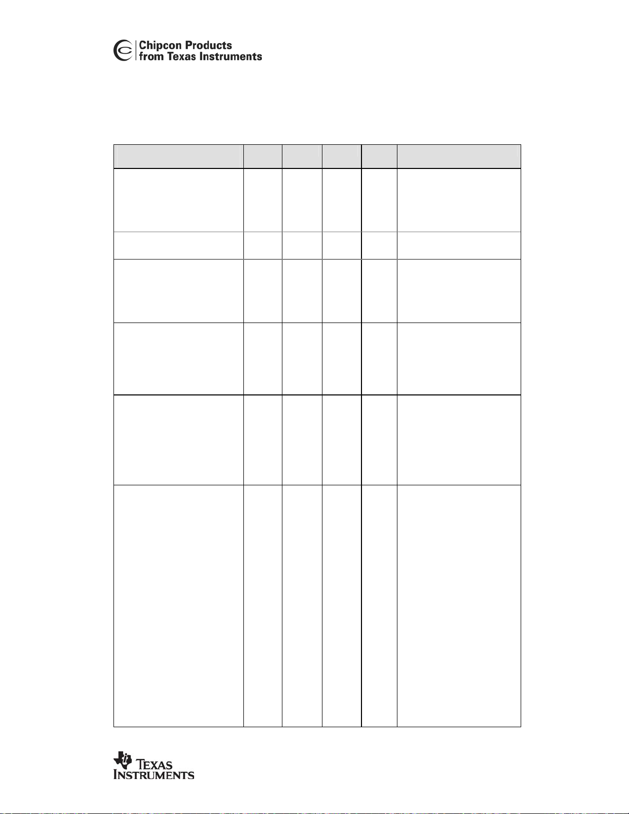
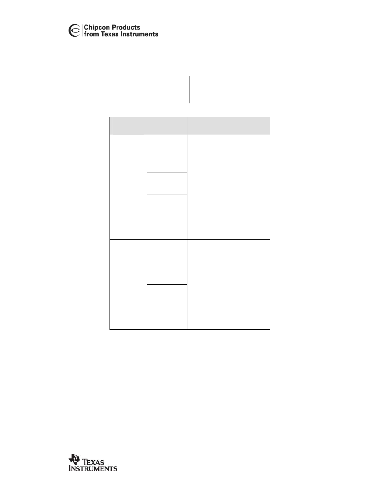
3 Absolute Maximum Ratings
Supply voltage, chip core,
AVDD/DVDD1.8=VDD
Supply voltage (DVDD3.3=VDDIO), digital I/O −0.3 3.6 V
Voltage on any pin, core −0.3 VDD+0.3,
Voltage on any pin, digital I/O (pin no. 27-35) −0.3 VDDIO+0.3,
Input RF level 10 dBm
Storage temperature range −50 150
Reflow solder temperature 260
NOTE:
The supply voltage to the chip core (AVDD/DVDD1.8) should not be switched off when the digital IO (DVDD3.3)
supply voltage is still applied to the chip. If this is done, a large current will flow inside the
be damaged as a result.
If the core supply needs to be switched off to lower the power consumption, please see page 17 for a suggested
solution.
The absolute maximum ratings given
above should under no circumstances be
violated. Stress exceeding one or more of
Parameter Min. Max. Units Condition
−0.3 2.0 V
max 2.0
max 3.6
V
V
°C
°C
CC2400
the limiting values may cause permanent
damage to the device.
Caution! ESD sensitive device.
Precaution should be used when handling
the device in order to prevent permanent
damage.
T = 10 s
and the chip may
4 Operating Conditions
Parameter Min. Typ. Max. Unit Condition
Supply voltage, chip core,
AVDD/DVDD1.8
Supply voltage (DVDD3.3), digital
I/O, VDDIO
Recommended supply voltage, chip
core, AVDD/DVDD1.8
Recommended supply voltage
(DVDD3.3), digital I/O
Operating ambient temperature
range
1.6 2.0 V
1.6 3.6 V The digital I/O voltage (DVDD3.3
1.8V
1.8V/
3.3V
−40 85
SWRS042A Page 6 of 83
pin) must match the interfacing
circuit.
°C
5 Electrical Specificati ons
CC2400
Parameter
Current Consumption,
Power Down mode (OFF)
Current Consumption,
Idle mode (IDLE)
Current Consumption,
Frequency synthesizer (FS_ON)
Current Consumption,
Receive mode
Current Consumption,
Transmit mode:
P=−25 dBm
P=−5 dBm
P=0 dBm
Current Consumption, crystal
oscillator core
Min. Typ. Max. Unit Condition / Note
1.5
1.2
6.3
24 mA
11
15
19
38
5
Oscillator core off
µA
mA
mA
mA
The output power is delivered
differentially to a 50Ω single-
mA
ended load through a balun, see
also p. 50.
mA
16 MHz, 16 pF load crystal
µA
Table 1 Electrical specifications
6 General Characteristics
Tc = 25°C, AVDD/DVDD1.8 = 1.8 V, DVDD3.3 = 3.3V (digital I/O) if nothing else stated. Measured on Chipcon’s
CC2400EM reference design.
Parameter
RF Frequency Range 2400
Data rate
Min. Typ. Max. Unit Condition / Note
10
250
1
2483 MHz Programmable in 1 MHz channel
kbps
Mbps
steps.
Data rate is
kbps
programmable/selectable, see
page 40
Table 2 General characteristics
SWRS042A Page 7 of 83
CC2400
7 RF Transmit section
Tc = 25°C, AVDD/DVDD1.8 = 1.8 V, DVDD3.3 = 3.3V (digital I/O) if nothing else stated. Measured on Chipcon’s
CC2400EM reference design.
Parameter
Binary FSK frequency deviation
Nominal output power 0 dBm Default settings.
Programmable output power range
Min. Typ. Max. Unit Condition / Note
0
250 500
25 dB
±kHz
The frequency corresponding to
the digital "0" is denoted f
f
corresponds to a digital "1".
1
The frequency deviation is given
by f
=±(f1−f0)/2. The RF carrier
d
frequency, f
f
=(f0+f1)/2.
c
Power delivered to a 50 Ω singleended load through a balun. The
output power is programmable in
8 steps.
, is then given by
c
0
, while
20 dB bandwidth
FSK
GFSK
Adjacent Channel Power (ACP)
FSK
GFSK
Harmonics
nd
2
order harmonic
rd
3
order harmonic
Spurious emission
30 - 1000 MHz
1– 12.75 GHz
1.8 – 1.9 GHz
5.15 – 5.3 GHz
Optimum load impedance 110
1.2
1.0
-30
-43
-41
-54
-65
-41
-69
-65
+ j130
Table 3 Transmit characteristics
-36
-30
-47
-47
MHz
MHz
dBc
dBc
dBm
dBm
dBm
dBm
dBm
dBm
Ω
Maximum output power.
Modulation is 1 Mbps, NRZ data,
± 250 kHz frequency deviation.
Maximum output power.
Modulation is 1 Mbps, NRZ data,
± 250 kHz frequency deviation.
Measured at 2 MHz offset.
At max output power delivered to
50 Ω single-ended load through a
balun. Carrier modulated with
pseudo-random data. See p.50.
Maximum output power.
Modulation is 1 Mbps FSK, NRZ
data, ±250 kHz frequency
deviation.
Complying with EN 300 440,
CFR47 Part 15 and ARIB STDT66
Differential impedance as seen
from the RF-port (RF_P and
RF_N) towards the antenna. For
matching details see “Input/
output matching” page 50 as well
as the application circuit
description on page 17.
SWRS042A Page 8 of 83
CC2400
8 RF Receive section
Tc = 25°C, AVDD/DVDD1.8 = 1.8 V, DVDD3.3 = 3.3V (digital I/O) if nothing else stated. Measured on Chipcon’s
CC2400EM reference design.
Parameter
Receiver Sensitivity at BER = 10−3
1 Mbps, 1 MHz channel BW
250 kbps, 1 MHz channel BW
10 kbps, 500 kHz channel BW
Saturation (maximum input level) 3 dBm Maximum gain in LNA.
Co-channel rejection
Adjacent channel rejection (ACR)
1 Mbps
250 kbps
Image channel rejection
1 Mbps
250 kbps
Selectivity (C/I)
(In-band channel rejection)
+ 2MHz
± 3MHz
± 4MHz
± 5MHz
± 10MHz
± 20 MHz
± 50MHz
+ 2 MHz
± 3 MHz
± 4 MHz
± 5 MHz
± 10 MHz
± 20 MHz
± 50 MHz
Min. Typ. Max. Unit Condition / Note
-87
-91
-101
-10 dB 1 Mbps wanted signal 10 dB
0
12
21
39
20
41
50
52
55
56
59
48
50
55
56
59
60
64
SWRS042A Page 9 of 83
Measured in a 50 Ohm singleended load through a balun. FSK,
NRZ mode used.
dBm
±250 kHz frequency deviation
dBm
±250 kHz frequency deviation
dBm
±125 kHz frequency deviation
NRZ coded data, BER = 10
above the sensitivity level,
interferer modulated like signal
(pseudo-random FSK, ± 250 kHz
deviation), interferer at operating
frequency, BER = 10
FSK wanted signal 10 dB above
the sensitivity level, 1 MHz
dB
channel spacing, interferer
dB
modulated like signal (pseudorandom FSK, ± 250 kHz
deviation) at adjacent channel,
BER = 10
FSK wanted signal 10 dB above
the sensitivity level, interferer
dB
modulated like signal (pseudo-
dB
random FSK, ± 250 kHz
deviation) at image frequency,
BER = 10
is centered 2MHz below the
center frequency of the desired
channel.
dB
1Mbps FSK wanted signal at
dB
2441 MHz, 3 dB above the
dB
sensitivity level (except + 2 MHz,
dB
which is 10 dB above the
dB
sensitivity limit), jammer
dB
modulated like signal (pseudo-
dB
random, ± 250 kHz deviation) at
± 2-39 MHz in 1 MHz steps
offset, BER = 10
channels and image channel are
excluded.
dB
250 kbps FSK wanted signal at
dB
2441 MHz, 3 dB above the
dB
sensitivity level (except + 2 MHz,
dB
which is 10 dB above the
dB
sensitivity limit), jammer
dB
modulated like signal (pseudo-
dB
random, ± 250 kHz deviation) at
± 2-39 MHz in 1 MHz steps
offset, BER = 10
channels and image channel are
excluded.
−3
−3
−3
. The image channel
−3
. Adjacent
−3
. Adjacent
−3
Parameter
Blocking / Desensitization*
(*out-of-band spurious response
rejection)
0.3 – 2.0 GHz
2.0 – 2.399 GHz
2.498 – 3.0 GHz
3 – 12.75 GHz
Input IIP3
Out of band
In band
Image frequency suppression
Spurious reception
Spurious emission
< 1 GHz
1 – 12.75 GHz
Min. Typ. Max. Unit Condition / Note
56 dB Ratio between sensitivity for a
80 dB Ratio between the sensitivity for
71
50
49
76
-5
-17
−70
−56
-57
-47
dB
dB
dB
dB
dBm
dBm
dBm
dBm
1 Mbps FSK wanted signal 3 dB
above the sensitivity level, sinewave interfering signal, BER =
−3
10
.
Measured directly by applying
two tones and measuring the
resulting difference tone
amplitude.
signal at the image frequency and
the sensitivity in the wanted
channel with an inverted signal.
The image frequency is centered
-2 MHz from the center of the
wanted channel. The signal
source is 1Mbps, NRZ coded
data, ±250 kHz frequency
deviation, signal level for BER =
−3
10
an unwanted frequency and the
sensitivity in the wanted channel.
The signal source is a 1 Mbps,
NRZ coded data, ±250 kHz
frequency deviation, swept over
all frequencies 2400 – 2483.5
MHz. Signal level for BER = 10
Adjacent channels and image
channel are excluded.
Complying with EN 300 440,
CFR47 Part 15 and ARIB STDT66
Table 4 RF Receive characteristics
CC2400
−3
9 AFC section
Parameter
AFC range
AFC accuracy 5 kHz
Min. Typ. Max. Unit Condition / Note
For 1Mbps and 1 MHz channel
± 500 kHz Measured using an unmodulated
Table 5 AFC characteristics
SWRS042A Page 10 of 83
width,
AFC_SETTLING=4.
carrier.
10 RSSI / Carrier Sense section
CC2400
Parameter
Min. Typ. Max. Unit Condition / Note
RSSI range / Carrier sense range
RSSI settling time 20 s
RSSI accuracy
For 1Mbps and 1 MHz channel
80 dB (The range is from –100 dBm to
± 4
dB See page 44 for details
Table 6 RSSI / Carrier sense characteristics
11 IF section
Parameter
Intermediate frequency (IF)
Digital channel filter bandwidth
Min. Typ. Max. Unit Condition / Note
1 MHz
125 1000 kHz The digital channel filter 6dB-
Table 7 IF characteristics
12 Frequency Synthesizer section
width.
–20 dBm typically)
bandwidth is programmable in
steps: 125, 250, 500 and 1000
kHz. See page 39 for details.
Parameter
Min. Typ. Max. Unit Condition / Note
Crystal oscillator frequency
Crystal frequency accuracy
requirement
Crystal operation
Crystal load capacitance
Crystal ESR
Crystal oscillator start-up time 1.13 ms 16 pF load
Phase noise
PLL loop bandwidth 50 kHz
16 MHz See page 49 for details.
20 ±ppm
Parallel C4 and C5 are loading
12 16 20 pF 16 pF recommended
60
-108
-114
-114
SWRS042A Page 11 of 83
dBc/Hz
dBc/Hz
dBc/Hz
The total crystal frequency
accuracy, i.e. initial tolerance plus
aging and temperature
dependency, will determine the
frequency accuracy of the
transmitted signal. 1 Mbps FSK,
250 kHz deviation.
capacitors, see page 49
Ω
Note: This time can be reduced to
15 s by enabling the XOSC core
in power-down using the
MANAND register.
Unmodulated carrier
At ±1 MHz offset from carrier
At ±2 MHz offset from carrier
At ±5 MHz offset from carrier
Parameter
PLL lock time (RX / TX turn-on
time)
PLL turn-on time from IDLE mode,
crystal oscillator on
Table 8 Frequency synthesizer characteristics
13 Digital Inputs/Outputs
CC2400
Min. Typ. Max. Unit Condition / Note
40
100
Until within ± 10 kHz
µs
Step size is 1MHz, no calibration.
Note: Calibration should be
performed for frequency changes
> 8 MHz.
Crystal oscillator running.
µs
Calibration time included.
Parameter
Min. Typ. Max. Unit Condition / Note
Logic "0" input voltage
Logic "1" input voltage
Logic "0" output voltage 0
Logic "1" output voltage 2.5
Logic "0" input current
Logic "1" input current
DIO setup time 20 ns TX un-buffered mode, minimum
DIO hold time
Serial interface (SCLK, SI, SO and
CSn) timing specification
Signal levels are referred to the
0 0.3*
0.7*
DVDD
NA −1
NA 1
10 ns TX un-buffered mode, minimum
See Table 12 page 22
DVDD
DVDD V
0.4 V Output current −8 mA,
DVDD V Output current 8 mA,
voltage level at the pin DVDD3.3.
V
3.3 V supply voltage
3.3 V supply voltage
Input signal equals GND
µA
Input signal equals DVDD
µA
time DIO must be ready before
the positive edge of DCLK
time DIO must be held after the
positive edge of DCLK
Table 9 Digital input/output characteristics
SWRS042A Page 12 of 83
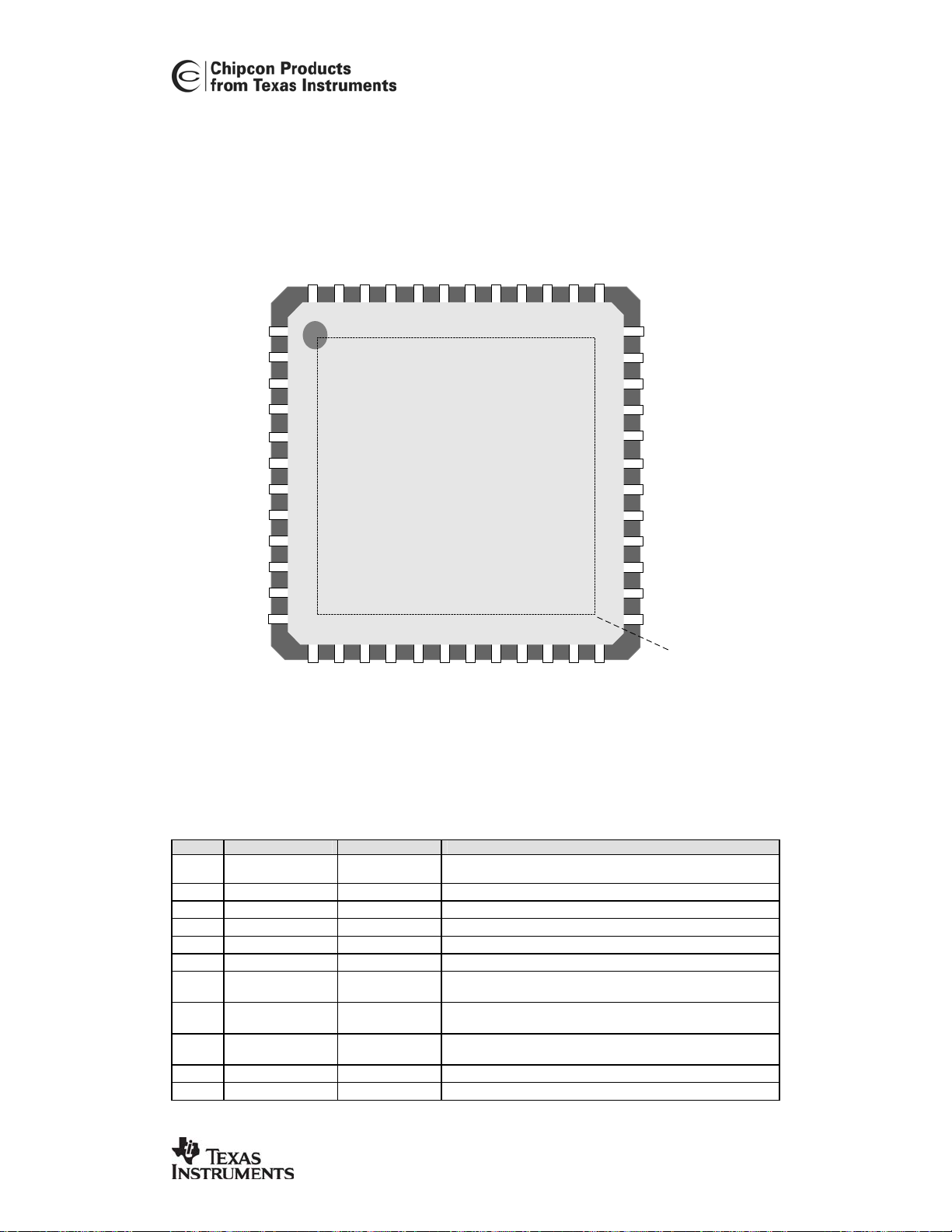
14 Pin Assignment
CC2400
VCO_GUARD
AVDD_VCO
AVDD_PRE
AVDD_RF1
GND
RF_P
TXRX_SWITCH
RF_N
GND
AVDD_SW
NC
NC
1
2
3
4
5
6
7
8
9
10
11
12
13
NC
AVDD_CHP
48
ATEST1
47
14
AVDD_RF2
R_BIAS
45
AVDD_IF1
44
ATEST2
46
QLP48
CC2400
15
16
17
DVDD_ADC
AVDD_ADC
AVDD_IF2
XOSC16_Q1
43
7x7
18
DGND_GUARD
XOSC16_Q2
42
19
DGUARD
AVDD_XOSC
41
20
BT/GR
NC
40
21
GIO1
22
DGND
NC
39
23
DSUB_PADS
NC
38
24
DSUB_CORE
NC
37
36
NC
35
GIO6
34
SO
33
SI
SCLK
32
31
CSn
30
DCLK/FIFO
29
DIO/PKT
28
TX
27
RX
26
DVDD1.8
25
DVDD3.3
AGND
Exposed die
attach pad
Figure 1
CC2400
Top View
Pin no. Pin name Pin type Description
- AGND Ground (analog)
1 VCO_GUARD Power (Analog) Connection of guard ring for VCO shielding
2 AVDD_VCO Power (Analog) Power supply for VCO
3 AVDD_PRE Power (Analog) Power supply for Prescaler
4 AVDD_RF1 Power (Analog) Power supply for RF front-end
5 GND Ground (Analog) Grounded pin for RF shielding
6 RF_P RF I/O Positive RF input/output signal to LNA/from PA in
7 TXRX_SWITCH Power (Analog) Common supply connection for RF front-end. Must be
8 RF_N RF I/O Negative RF input/output signal to LNA/from PA in
9 GND Ground (Analog) Grounded pin for RF shielding
10 AVDD_SW Power (Analog) Power supply connection
Exposed die attach pad. Must be connected to solid ground
plane
receive/transmit mode
connected to RF_P and RF_N externally through a DC path.
receive/transmit mode
SWRS042A Page 13 of 83
CC2400
Pin no. Pin name Pin type Description
11 NC --- No Connect
12 NC --- No Connect
13 NC --- No Connect
14 AVDD_RF2 Power (Analog) Power supply for receive and transmit mixers
15 AVDD_IF2 Power (Analog) Power supply for transmit IF chain
16 AVDD_ADC Power (Analog) Power supply connection of ADCs and DACs
17 DVDD_ADC Power (Digital) Power supply for digital part of receive ADCs
18 DGND_GUARD Ground (Digital) Ground connection for digital noise isolation
19 DGUARD Power (Digital) Power supply connection for digital noise isolation
20 BT/GR Digital Input Selection of Built-in-Test or Generic Radio (normal operation).
21 GIO1 Digital I/O General digital I/O pin. Configure as output when not used.
22 DGND Ground (Digital) Ground connection for digital modules
23 DSUB_PADS Ground (Digital) Substrate connection for digital I/O’s
24 DSUB_CORE Ground (Digital) Substrate connection for digital modules
25 DVDD3.3 Power (Digital) Power supply for digital I/O’s
26 DVDD1.8 Power (Digital) Power supply for digital modules
27 RX Digital Input Strobe signal for RX mode. Connect to ground when not used.
28 TX Digital I/O Strobe signal for TX mode. Connect to ground when not used.
29 DIO/PKT Digital I/O Data input/output in un-buffered mode or packet handling
30 DCLK/FIFO Digital Output Data clock output signal in un-buffered mode or FIFO control
31 CSn Digital Input SPI: Chip Select
32 SCLK Digital Input SPI: Serial data clock
33 SI Digital Input SPI: Slave Input
34 SO Digital Output SPI: Slave Output
35 GIO6 Digital Output General digital output pin. See Table 18
36 NC --- No Connect
37 NC --- No Connect
38 NC --- No Connect
39 NC --- No Connect
40 NC --- No Connect
41 AVDD_XOSC Power (Analog) Power supply for 16 MHz crystal oscillator
42 XOSC16_Q2 Analog output 16 MHz crystal oscillator
43 XOSC16_Q1 Analog input 16 MHz crystal oscillator or external clock input
44 AVDD_IF1 Power (Analog) Power supply connection of receive IF chain
45 R_BIAS Analog Output Connection for external precision bias resistor
46 ATEST2 Analog I/O Analog test I/O for prototype and production testing. Leave not
47 ATEST1 Analog I/O Analog test I/O for prototype and production testing. Leave not
48 AVDD_CHP Power (Analog) Power supply for phase detector and charge pump
NOTES:
The exposed die attach pad must be connected to a solid ground plane as this is the main ground connection for the
chip.
The digital inputs SCLK, SI and CSn are high-impedance inputs (no internal pull-up) and should have external pullups if not driven. RX and TX should have external pull-down if not driven (to prevent the state machine from being
trigged). SO is high-impedance when CSn is high. External pull-up should be used at SO to prevent floating input at
the microcontroller.
Connect to ground for normal operation (NOTE: For Chipcon
internal use only.)
See Table 18
control signal. Configure as output when not used.
signal. Leave open when not used.
connected when not used.
connected when not used.
SWRS042A Page 14 of 83
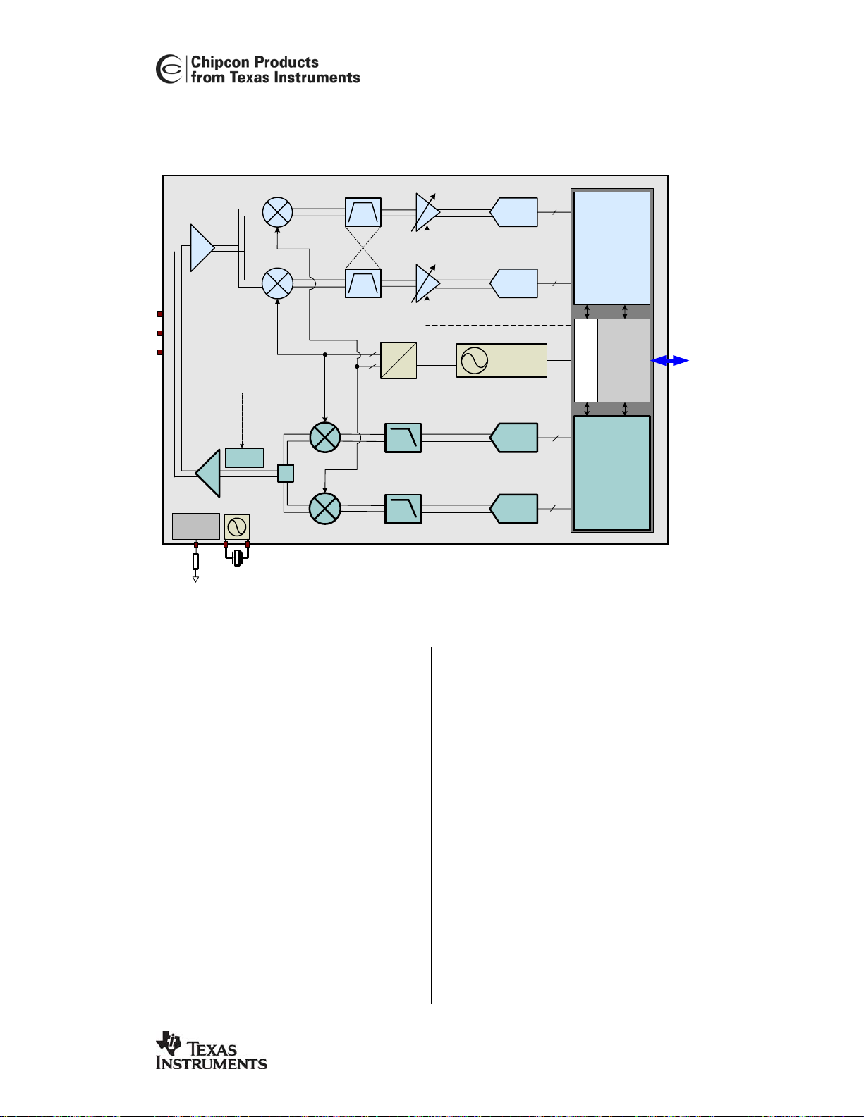
15 Circuit Description
CC2400
LNA
TX/RX CONTROL
SmartRF
CC2400
0
90
Power
Control
PA
On-chip
XOSC
BIAS
16 MHz
A simplified block diagram of
shown in Figure 2.
CC2400
features a low-IF receiver. The
received RF signal is amplified by the lownoise amplifier (LNA) and down-converted
in quadrature (I and Q) to the intermediate
frequency (IF). At IF (1 MHz), the I/Q
signal is filtered and amplified, and then
digitized by the ADCs. Automatic gain
control, final channel filtering,
demodulation and bit synchronization is
performed digitally.
CC2400
outputs (in un-buffered mode only)
the digital demodulated data on the DIO
pin. A synchronized data clock is then
available at the DCLK pin. In buffered
mode the demodulated data is sent to a
FIFO and is accessible through the SPI
interface. RSSI is available in digital
format and can be read via the serial
interface. The RSSI also features a
Σ
Figure 2.
CC2400
CC2400
is
simplified block diagram
SWRS042A Page 15 of 83
ADC
ADC
AGC CONTROL
FREQ
SYNTH
TX POWER CONTROL
DAC
DIGITAL
DEMODULATOR
- Digital RSSI
- Gain Control
- Image Suppression
- Channel Filtering
- Demodulation
DIGITAL
INTERFACE /
FIFO
CONTROL LOGIC
DIGITAL
MODULATOR
- Data Filtering
- Modulation
- Power Control
DAC
programmable carrier sense indicator with
output on either GIO1 or GIO6.
In transmit mode the baseband signal is
directly up-converted quadrature (I and Q)
and then fed to the power amplifier (PA).
The TX IF signal is frequency shift keyed
(FSK). Optionally Gaussian filtering can be
used enabling GFSK. The BT of the
Gaussian filter is 0.5 for a datarate of
1 Mbps.
The internal T/R switch circuitry simplifies
the antenna interface and matching. The
antenna connection is differential. The
biasing of the PA and LNA is done by
connecting TXRX_SWITCH to RF_P and
RF_N through an external DC path.
The frequency synthesizer includes a
completely on-chip LC VCO and a 90
degrees phase splitter for generating the
TO MICROCONTROLLER

LO_I and LO_Q signals to the downconversion mixers in receive mode and
up-conversion mixers in transmit mode.
The VCO operates in the frequency range
4800 – 4966 MHz, and the frequency is
divided by two when split in I and Q.
A crystal must be connected to
XOSC16_Q1 and XOSC16_Q2 and
generates the reference frequency for the
CC2400
synthesizer. A PLL lock signal is available
via the GIO pins.
The digital baseband includes support for
packet handling and data buffering.
The 4-wire SPI serial interface is used for
configuration (and data interface in
buffered mode). A few digital I/O lines can
be configured for use with packet handling
strobe and interrupt signals.
SWRS042A Page 16 of 83

16 Application Circuit
Few external components are required for
CC2400
the operation of
application circuit is shown in Figure 3. A
description of the external components
referring to Figure 3 are described in
Table 10. The bill of materials (BOM) is
given in Table 11.
Good PCB layout is vital for proper
operation, please see the section on PCB
Layout Recommendations on page 56 for
more details.
16.1 Input / output matching
The RF input/output is high impedance
and differential. The optimum differential
load for the RF port is listed on page 8.
When using an unbalanced antenna like a
monopole, a balun should be used in
order to get optimum performance. The
balun can be implemented using low-cost
discrete inductors and capacitors. The
balun consists of C61, C62, C71, C81,
L61, L62 and L72, and will match the RF
input/output to 50 Ω, see Figure 3. L61
and L62 also provide DC biasing of the
LNA/PA input/output. L71 is used to
isolate the TXRX_SWITCH pin. An
internal T/R switch circuit is used to switch
between the LNA and the PA. See
“Input/output matching” on page 50 for
more details.
If a balanced antenna, like a folded dipole,
is used, the balun can be omitted. If the
antenna also provides a DC path from the
TXRX_SWITCH pin to the RF pins,
inductors are not needed for DC biasing.
The L71 isolation inductor should still be
used to avoid antenna reflections. Figure 4
shows a typical application circuit with
differential antenna. The dipole has a
virtual ground point, hence bias is
provided without degradation in antenna
performance. Please note that a
differential antenna is generally larger than
an equivalent single-ended antenna.
. A typical
CC2400
16.3 Crystal
An external crystal with input and output
loading capacitors (C421 and C431) is
used for the crystal oscillator. See page 49
for details.
16.4 Digita l I/O
The supply voltage for the digital I/O must
match the interfacing microcontroller. The
digital I/Os of
microcontrollers with supply voltages in
the range 1.6 – 3.6 V.
16.5 Power supply decoupling and
filtering
Proper power supply decoupling must be
used for optimum performance. The
placement and size of the decoupling
capacitors and the power supply filtering
are very important to achieve the best
performance in an application. Chipcon
provides a compact reference design that
should be followed very closely.
16.6 Power supply switching
As described in a note in the Absolute
Maximum Ratings section, the voltage
supply to the chip core should not be
switched off separately from the I/O supply
voltage.
If it is necessary to switch the core power
supply off, for instance to save the power
dissipated in the 1.8V regulator, the I/O
supply should be turned off as well. This
can be done quite easily by running the
I/O supply from a microcontroller I/O pin.
Current drawn on the I/O supply is just a
few milliamps, so an ordinary I/O pin
should have no problems in sourcing this
current. Power sequencing should be
performed so that both supplies are turned
on and off simultaneously.
CC2400
can interface
16.2 Bias resistor
The bias resistor R451 is used to set an
accurate bias current for the chip.
SWRS042A Page 17 of 83
CC2400
Ref Description
C71 Front-end bias decoupling and match, see page 50
C61 Discrete balun and match, see page 50
C81 Discrete balun and match, see page 50
C62 DC block to antenna and match
C421 16MHz crystal load capacitor, see page 49
C431 16MHz crystal load capacitor, see page 49
L61 DC bias and match, see page 50
L62 DC bias and match, see page 50
L71 RF blocking inductor, see page 50
L81 Discrete balun and match, see page 50
R451 Precision resistor for current reference generator
XTAL 16MHz crystal, see page 49
Table 10. Overview and description of external components for an unbalanced antenna
(balun implemented with low cost discrete components)
AVDD=1.8V
AVDD=1.8V
AVDD=1.8V
48
AVDD
_CHP
C431 C421
R451
47
46
R_BIAS
ATEST2
ATEST1
XTAL
44
43
42
45
AVDD_IF1
41
XOSC16_Q2
XOSC16_Q1
AVDD_XOSC
NC
38
39
NC
NC
37
NC
40
Antenna
(50 Ohm)
C62
C61
C71
L81
L62
L61
C81
AVDD=1.8V
L71
10
11
12
1
VCO_GUARD
2
AVDD_VCO
3
AVDD_PRE
4
AVDD_RF1
5
GND
6
RF_P
7
TXRX_SWITCH
8
RF_N
9
GND
AVDD_SW
NC
NC
NC
CC2400
DCLK/FIFO
DGND_GUARD
DVDD_ADC
AVDD_ADC
AVDD_RF2
AVDD_IF2
15
16
14
13
DGUARD
BT/GR
GIO1
20
18
19
17
21
DVDD=1.8V
DGND
22
DSUB_PADS
23
DSUB_CORE
DVDD1.8
DVDD3.3
24
NC
GIO6
SO
SCLK
CSn
DIO/PKT
TX
RX
36
35
34
33
SI
32
31
30
29
28
27
26
25
Figure 3 Typical application circuit with discrete balun for interfacing single-ended
antenna
SPI-bus
Optional
digital
interface
DVDD=1.8V
DVDD Digital I/O
=1.8 / 3.3V
SWRS042A Page 18 of 83
CC2400
AVDD=1.8V
AVDD=1.8V
AVDD=1.8V
48
AVDD
_CHP
C431 C421
R451
47
46
R_BIAS
ATEST2
ATEST1
XTAL
44
43
42
45
AVDD_IF1
41
XOSC16_Q2
XOSC16_Q1
AVDD_XOSC
NC
38
39
NC
37
NC
40
NC
Folded
dipole
antenna
L61
AVDD=1.8V
L71
1
VCO_GUARD
2
AVDD_VCO
3
AVDD_PRE
4
AVDD_RF1
5
GND
6
RF_P
7
TXRX_SWITCH
8
RF_N
9
GND
10
AVDD_SW
11
NC
12
NC
NC
CC2400
DCLK/FIFO
DIO/PKT
DGND_GUARD
DVDD_ADC
AVDD_ADC
AVDD_RF2
AVDD_IF2
15
16
14
13
DGUARD
BT/GR
GIO1
20
18
19
17
21
DVDD=1.8V
DSUB_CORE
DSUB_PADS
DGND
22
DVDD1.8
DVDD3.3
24
23
NC
GIO6
SCLK
CSn
SO
TX
RX
36
35
34
33
SI
32
31
30
29
28
27
26
25
Figure 4 Typical application circuit with differential antenna (folded dipole)
Item Single ended output, discrete
Differential antenna
balun
C62 5.6 pF, +/- 0.25pF, NP0, 0402 Not used
C61 0.5 pF, +/- 0.25pF, NP0, 0402 Not used
C81 0.5 pF, +/- 0.25pF, NP0, 0402 Not used
C71 100 nF, 10%, X5R, 0402 100 nF, 10%, X5R, 0402
C421 18 pF, 5%, NP0, 0402 18 pF, 5%, NP0, 0402
C431 18 pF, 5%, NP0, 0402 18 pF, 5%, NP0, 0402
L61 7.5 nH, 5%, Monolithic/multilayer, 0402 27 nH, 5%, Monolithic/multilayer, 0402
L62 5.6 nH, 5%, Monolithic/multilayer, 0402 Not used
L71 27 nH, 5%, Monolithic/multilayer, 0402 27 nH, 5%, Monolithic/multilayer, 0402
L81 7.5 nH, 5%, Monolithic/multilayer, 0402 Not used
R451
43 kΩ, 1%, 0402 43 kΩ, 1%, 0402
XTAL 16 MHz crystal, 16 pF load (CL) 16 MHz crystal, 16 pF load (CL)
NOTE: Decoupling components are not included.
Table 11. Bill of materials for the appl icati on circuits
SPI-bus
Optional
digital
interface
DVDD=1.8V
DVDD Digital I/O
=1.8 / 3.3V
SWRS042A Page 19 of 83
17 Configuration Overview
CC2400
can be configured to achieve
optimum performance for different
applications. Through the programmable
configuration registers the following key
parameters can be programmed:
• Receive / transmit mode
• RF frequency
• RF output power
• FSK frequency deviation
• Power-down / power-up mode
18 Configuration Software
CC2400
• Crystal oscillator power-up / power
down
• Data rate and line coding (NRZ,
8B/10B coding)
• Synthesizer lock indicator mode
• Digital RSSI
• FSK / GFSK modulation
• Data buffering
• Packet handling hardware support
Chipcon provides users of
software program, SmartRF
(Windows interface) that generates all
necessary
based on the user's selections of various
parameters. These hexadecimal numbers
will then be the necessary input to the
CC2400
configuration data,
CC2400
®
Studio
with a
microcontroller for the configuration of
CC2400
.
Figure 5 shows the user interface of the
CC2400
configuration software.
Figure 5. SmartRF
®
Studio user interface
SWRS042A Page 20 of 83

19 4-wire Serial Configuration Interface
CC2400
CC2400
is configured via a simple 4-wire
SPI-compatible interface (SI, SO, SCLK
and CSn) where
interface is also used as data interface in
buffered mode (see page 27).
There are 44 16-bit configuration registers,
9 Command Strobe Registers, and one
register to access the FIFO. Each register
has a 7-bit address. The FIFO (32 bytes)
is 8 bits wide. A Read/Write bit indicates a
read or a write operation and forms the 8bit address field together with the 7-bit
address.
Some registers are termed Command
Strobe Registers. By addressing a
Command Strobe register internal
sequences will be started. These
commands can be used to quickly change
from RX mode to TX mode, for example.
A full configuration of
sending 44 data frames of 24 bits each (7
address bits, R/W bit and 16 data bits).
The time needed for a full configuration
depend on the SCLK frequency. With a
SCLK frequency of 20 MHz the full
configuration is done in less than 5 µs.
Setting the device in power down mode
requires addressing one command strobe
register only, and will in this case take less
than 0.4 µs. All registers except the strobe
registers are also readable.
In each write-cycle, 24 bits are sent on the
SI-line. The bit to be sent first is the R/W
bit (0 for write, 1 for read). The next seven
bits are the address-bits (A6:0). A6 is the
MSB (Most Significant Bit) of the address
and is sent first. The 16 data-bits are then
transferred (D15:0). During address and
data transfer the CSn (Chip Select, active
low) must be kept low. See Figure 6.
The timing for the programming is shown
in Figure 6 with reference to Table 12. The
clocking of the data on SI into the
is performed on the positive edge of
SCLK.
CC2400
is the slave. This
CC2400
requires
CC2400
The data word is loaded into the internal
configuration register, when the last bit,
D0, of the 16 data bits has been written.
The configuration data will be retained
during a programmed power-down mode,
but not when the power-supply is turned
off. The registers can be programmed in
any order.
The configuration registers can also be
read by the microcontroller via the same
configuration interface. The R/W bit must
be set high
then the seven address bits are sent.
CC2400
addressed register. SO is used as the
data output and must be configured as an
input by the microcontroller.
The command strobe register is accessed
in the same way as for a write operation,
but no data is transferred. That is, only the
R/W bit and the seven address bits are
written before CSn should be set high.
Figure 7 shows a summary of read and
write operations. A register read/write can
be terminated after one byte if only the
most significant byte is required. A register
can also be accessed repeatedly without
writing the address again. The buffer FIFO
(8 bit wide, 32 bytes) can be written
continuously by simply writing new bytes
over and over. The internal data pointer is
then updated for every written byte. The
session is terminated when the CSn is set
high.
Please note that a longer hold time, t
needed before setting CSn high when
accessing the FIFO in buffered mode.
During the transfer of the address, the
CC2400
line containing some important flags. This
is shown in Table 13.
to initiate the data read-back,
then returns the data from the
, is
ps
returns a status byte on the SO
SWRS042A Page 21 of 83
t
sp
SCLK:
CSn:
Write to register:
SI
SO
Read from register:
SI
SO
Read or write a w hole register (16 bit):
Read or write 8 MSB of a register:
Read or write a whole register continuously:
Read or write n bytes from/to RF FIFO:
t
t
ch
cl
A6 A5 A4 A3 A2 A0A1 DW15 DW14 DW13 DW12 DW11 DW10 DW9 DW8 DW7 DW6 DW5 DW4 DW3 DW2 DW1 DW0
0
S7 S6 S5 S4 S3 S2 S0S1
A6 A5 A4 A3 A2 A0A1
1
Command strobe:
Figure 7. Configuration registers write and read operations via SPI
t
sd
X X X
DR15 DR14 DR13 DR12 DR11 DR10 DR9 DR8 DR7 DR6 DR5 DR4 DR3 DR2 DR1 DR0S7 S6 S5 S4 S3 S2 S0S1
Figure 6. SPI timing diagram
CSn:
ADDR
DATA
ADDR DATA
ADDR
ADDR DATA
ADDR
FIFO
DATA
DATA
DATA
8MSB
8MSB
8MSB
byte0
DATA
8LSB
8LSB
byte1
DATA
DATA
CC2400
t
ps
t
hd
X
X
8MSB
byte2
DATA
DATA
8LSB
byte3
DATA
...
8MSB
DATA
...
byte n-2
DATA
DATA
t
ns
DR15
8LSB
byte n-1
Parameter Symbol Min Max Units Conditions
SCLK, clock
frequency
SCLK low
pulse
duration
SCLK high
pulse
duration
CSn setup
time
CSn hold
time 1
CSn hold
time 2
SI setup time t
SI hold time
Rise time t
Fall time t
Note: The set-up- and hold-times refer to 50% of VDD.
f
SCLK
t
25 ns The minimum time SCLK must be low.
cl,min
t
25 ns The minimum time SCLK must be high.
ch,min
t
sp
20 MHz
25 ns The minimum time CSn must be low before
positive edge of SCLK.
tns 25 ns The minimum time CSn must be held low after the
last negative edge of SCLK.
tps 300 ns In buffered mode: The minimum time CSn must be
held low after the last positive edge of SCLK. This
only applies to FIFO accesses.
sd
25 ns The minimum time data on SI must be ready
before the positive edge of SCLK.
thd 25 ns The minimum time data must be held at SI, after
the positive edge of SCLK.
100 ns The maximum rise time for SCLK and CSN
rise
100 ns The maximum fall time for SCLK and CSn
fall
Table 12. SPI timing specification
SWRS042A Page 22 of 83
Bit # Name Description
7 -
6 XOSC16M_STABLE
5 RESERVED
4 SYNC_RECEIVED
3 CRC_OK
2 FS_LOCK
1:0 RESERVED[1:0]
Table 13. Status byte returned during address transfer
Reserved, ignore value
Indicates whether the 16 MHz oscillator is running ('1') or not
Reserved
Indicates whether a sync word has been received or not so far in
the RX operation
Indicates whether the next two bytes in the FIFO will make the
CRC calculation successful or not:
0: CRC not OK or CRC off
1: CRC OK
Indicates whether the frequency synthesiser is in lock ('1') or not.
Reserved
CC2400
SWRS042A Page 23 of 83
20 Overview of Configurations and Hardware Support
CC2400
The
CC2400
can be configured for different
data interfaces, coding schemes and
packet handling hardware support.
Data
Data coding Packet handling support
interface
Buffered
(32 byte FIFO
accessed
through the
SPI interface)
Un-buffered
(DIO and
DCLK
synchronous
interface)
NRZ
8/10 code
Manchester
NRZ
Table 14 below gives a summary of the
possibilities.
TX:
• Preamble generation
• Sync word insertion
• CRC computation and insertion
RX:
• Sync Word detection
• CRC computation and check
RX:
• Sync Word detection
Manchester
Table 14. Configurations and hardware support
SWRS042A Page 24 of 83
21 Microcontroller Interfa ce and Pin Configuration
CC2400
Used in a typical system,
interface to a microcontroller. This
microcontroller must be able to:
• Program
and read back status information via
the 4-wire SPI-bus configuration
interface (SI, SO, SCLK and CSn). In
buffered mode the data signal is also
transmitted through the SPI-bus
• Interface to the bi-directional
synchronous data signal interface (DIO
and DCLK) if un-buffered data
transmission is to be used
• Optionally interface to the general
control and status pins (RX, TX, FIFO,
PKT, GIO1 and GIO6) if the hardware
supported packet handling functions
are to be used
• Optionally the microcontroller can
monitor the general I/O pins (GIO1,
GIO6) for frequency lock status, carrier
sense status, or other status
information
• Optionally, the microcontroller can read
back digital RSSI value and other
status information via the 4-wire SPI
interface
21.1 Configuration interface
The microcontroller interface is shown in
Figure 8. The microcontroller uses a
minimum of 4 I/O pins for the SPI
configuration interface (SI, SO, SCLK and
CSn). All other pins are optional. SO
should be connected to an input at the
microcontroller. SI, SCLK and CSn must
be microcontroller outputs.
The microcontroller pins connected to SI,
SO and SCLK can be shared with other
SPI-interface devices. SO is a high
impedance output as long as CSn is not
activated (active low).
CSn should have an external pull-up
resistor or be set to a high level during
power down mode in order to prevent the
input from floating. SI and SCLK should be
set to a defined level to prevent the input
from floating.
CC2400
into different modes
CC2400
will
SWRS042A Page 25 of 83
21.2 Signal interface in un-buffered
mode
A bi-directional pin (DIO) is used for data
to be transmitted and received. DCLK
providing the data timing should be
connected to a microcontroller input.
The data is clocked in/out at the positive
edge of DCLK.
21.3 General control and status pins
Optionally, in buffered mode, the FIFO pin
can be used to interrupt the
microcontroller at full/empty FIFO. This pin
should then be connected to a
microcontroller interrupt pin.
Optionally, using the packet handling
support, the PKT pin can be used in
buffered mode to interrupt the
microcontroller when a sync word is
detected (RX mode) and packet is
transmitted (TX mode). This pin should
then be connected to a microcontroller
interrupt pin.
The polarity of FIFO and PKT can be
controlled by the INT register (address
0x23).
Optionally, the RX and TX pins can be
used to change the operating mode of
CC2400
as an alternative to using the SPI
interface strobe commands. These pins
should then be connected to
microcontroller output pins. If the RX and
TX pins are not used, they should be
grounded in order to prevent accidental
change of mode.
Optionally, the GIO1 and GIO6 can be
used to monitor several status signals as
selected by the IOCFG register. The GIO6
pin should be connected to a
microcontroller input pin. See Table 18 for
available signals.
Table 15 gives a summary of the possible
pin configurations in the different operation
modes.
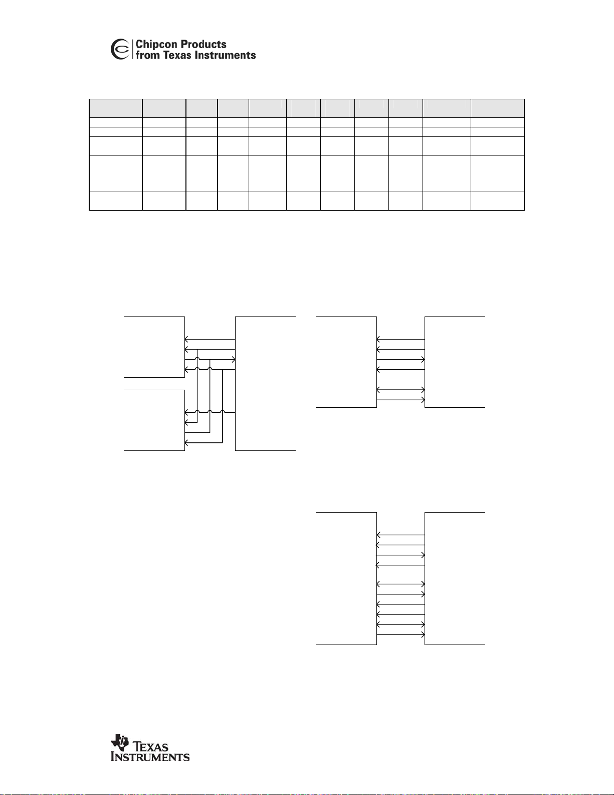
CC2400
Pin name SCLK SI SO CSn DIO/
Pin number 32 33 34 31 29 30 27 28 21 35
Direction I I O I I/O O I I O O
Buffered
mode
Buffered
mode with
Packet
handling
Un-buffered
mode
SCLK SI SO CSn - FIFO (RX) (TX) (GIO1) (GIO6)
SCLK SI SO CSn PKT FIFO (RX) (TX) (GIO1) (GIO6)
SCLK SI SO CSn DIO DCLK (RX) (TX) (GIO1) (GIO6)
PKT
NOTE: Pin functions in parentheses are optional
* The use of GIO1 and GIO6 are selected in register IOCFG (address 0x08)
Table 15. Pin configuration
Buffered RF Mode: Unbuffered RF Mode:
CC2400 µC
CSn
SCLK
SO
Data &
Control
SI
GIO1
MOSI
MISO
SCLK
DCLK/
FIFO
RX TX GIO1* GIO6*
CC2400 µC
SCLK
CSn
SO
Control
GIO1
SI
MOSI
MISO
SCLK
Other Circuit
CSn
SCLK
SO
DIO/PKT
DCLK/FIFO
TX
Data
Data &
Control
GIO1
SI
Control
MOSI
MISO
SCLK
GIO2DIO/PKT
GIO3
GIO4RX
GIO5
GIO6GIO1
GIO2
SI
Full hardware support for packet handling :
CC2400 µC
CSn
SO
SCLK
DCLK/FIFO
GIO6 GIO7
Figure 8. Microcontroller interface
SWRS042A Page 26 of 83

22 Data Buffering
CC2400
The
CC2400
un-buffered data interface. The data
buffering mode is controlled by the
GRMDM.PIN_MODE[1:0] bits (register
address 0x20).
In un-buffered mode a synchronous data
clock is provided by
pin, and the DIO pin is used as data
input/output (see Figure 8).
22.1 Buffered mode
In the buffered mode a 32-byte First-in
First-Out (FIFO) register block is used for
data to be transmitted and data received.
The FIFO is accessed through the
FIFOREG register (address 0x70) using
the SPI interface. Multiple bytes can be
written to the FIFO without repeating the
address if the CSn line is held low.
The crystal oscillator must be running
when accessing the FIFO.
By using the FIFO buffer the data can be
transmitted in bursts. The buffered mode
will therefore offload the host controller
keeping the SPI data rate much lower than
the data rate on the air. This gives also a
great advantage in reducing the current
consumption as the transmitter and
receiver are enabled only in short periods.
It also allows the SPI to operate faster
than the data rate, providing more time for
the MCU to work between data transfers.
More than 32 bytes can be received if the
FIFO is read during reception. In the same
way more than 32 bytes can be
transmitted if new data is written into the
FIFO during transmission. Figure 9 shows
the ways the FIFO can be used during
transmission.
22.2 Buffered mode hardware support
In the buffered mode the FIFO pin can be
used as an interrupt output to assist the
microcontroller in supervising the FIFO.
The FIFO pin can be programmed to give
an interrupt when the FIFO is nearly
empty in TX mode, and nearly full in RX
can be used with a buffered or
CC2400
at the DCLK
mode. The threshold (FIFO_THRESHOLD)
is set in INT.FIFO_THRESHOLD[4:0].
In receive mode there will be an interrupt
when the number of received bytes in the
FIFO reaches FIFO_THRESHOLD. The
default value is 30, giving an interrupt
when 30 bytes are received. If the FIFO
becomes full (32 bytes) before it is read,
the reception will be terminated (goes to
the FS_ON state).
In transmit mode there will be an interrupt
when the number of bytes left in the FIFO
reaches 32 - FIFO_THRESHOLD. For the
default value this will happen when there
are 2 bytes left. The transmission is
terminated when the FIFO runs empty
(goes to the FS_ON state). Note that in
order for the FIFO pin to give an interrupt
in transmit mode the number of bytes
must first exceed 32 - FIFO_THRESHOLD.
The FIFO pin activity is illustrated in
Figure 10.
The INT.FIFO_POLARITY bit sets the
polarity of the interrupt signal.
In TX mode, the FIFO pin goes low when
a transmission starts and the preamble is
sent. It will stay low as long as the FIFO is
empty. When data is written to the FIFO, it
will go high. If the number of bytes in the
FIFO goes below the FIFO_THRESHOLD,
the FIFO pin will go low again. If the FIFO
pin goes low, it will stay low until the CRC
has been transmitted.
FIFO_FULL and FIFO_EMPTY signals are
available on the general-purpose I/O pins.
These two signals are affected by
FIFO_THRESHOLD.
In transmit mode, FIFO_EMPTY is low if
the number of bytes in the FIFO is more
than 32-FIFO_THRESHOLD. In receive
mode, FIFO_EMPTY goes low when there
is more than 1 byte in the FIFO.
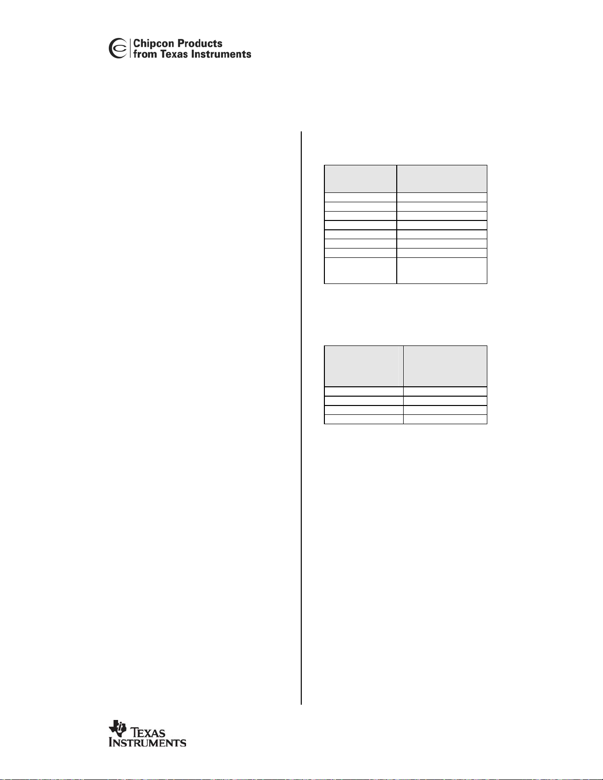
SWRS042A Page 27 of 83

FIFO_FULL is high if the number of bytes
in the FIFO is greater or equal to
FIFO
FIFO_THRESHOLD.
CC2400
Data to
pack et
engine
Packet #0
Data
from
MC U
a) Single packet in FIF O
FIFO
Dat a already sent
Packet #0
to pac ket engine
b) Pack et longer than F IFO
Data
pending
from MCU
Figure 9. Ways in which the FIFO can be used during transmit mode
r
e
d
n
u
o
g
s
e
t
y
b
d
l
o
O
h
F
I
s
e
r
h
t
RF data
d
e
t
c
,
d
e
e
b
e
k
c
o
b
r
o
o
t
l
r
s
t
L
s
N
L
X
P
O
R
S
S
F
Preamble Sync word Data
e
t
e
d
d
r
o
w
c
n
y
S
F
h
c
a
e
r
s
e
t
y
b
d
l
o
O
h
F
I
s
e
r
h
t
F
RX mode:
TX mode:
PKT
FIFO
e
b
o
r
t
s
c
o
l
N
L
O
L
S
X
P
F
T
S
MCU data
PKT
FIFO
Figure 10. FIFO and PKT timing diagram
n
o
h
c
a
e
r
,
d
e
k
e
b
o
r
t
s
s
e
t
y
b
d
l
o
O
h
F
I
s
F
e
r
h
t
y
t
p
m
e
O
F
a
I
P
F
i
s
s
i
m
s
n
a
r
t
t
e
e
t
k
e
l
c
p
m
o
c
SWRS042A Page 28 of 83
23 Packet Handling Hardware Support
CC2400
The
CC2400
has built-in hardware support
for packet oriented radio protocols.
The buffered mode packet handling
support can in transmit mode be used to
construct the data packet:
• Add a programmable number of
preamble bytes
• Add a synchronization word
• Compute and add a CRC
computed over the data field
In receive mode the packet handling
support can be used to de-construct the
data packet:
• Synchronization word detection
• Compute and check the received
CRC
The packet handling support can be
combined with the 8/10 line-encoding
scheme. The 8/10 coding will apply to the
data field (FIFO data) of the packet only
(and CRC).
In un-buffered mode the synchronization
word detection can be used to mute DCLK
until a valid sync word is received.
23.1 Data packet format
The format of the data packet can be
configured, and can consist of the
following items:
• Preamble
• Synchronization word
• Data
• CRC
See Table 16 and Figure 11 for details.
The preamble pattern is ‘(0)101010…’.
The first bit in the preamble is always the
same as the first bit in the synchronization
word. The length of the preamble is
programmable. The default and
recommended length is 4 bytes.
When using GFSK modulation at 1 Mbps,
Chipcon recommends using a preamble
length of 32 bytes in order to avoid a high
level of bit errors. If low packet overhead
SWRS042A Page 29 of 83
is required, Chipcon recommends that
FSK be used at 1 Mbps instead of GFSK.
GRMDM.
PRE_BYTES[2:0]
000 0*
001 1
010 2
011 4
100 8
101 16
110 32
111 Infinitely until TX
* Should not be used if packet reception is to be
used. Use to terminate infinite transmission (111).
The length of the synchronization word is
programmable as shown below.
Number of bytes
(8 bits)
GRMDM.PRE_BYTES
[2:0] is set to 000
GRMDM.
SYNC_WORD_SIZE
[1:0]
00 8
01 16
10 24
11 32
The synchronization word is
programmable in the SYNCL and SYNCH
registers. The default (and recommended)
synchronization word length is 32 bits,
which gives high immunity against false
synchronization word indication. If lower
immunity can be accepted, one can
reduce the length to 16 bits. (However,
using 8 bits will typically give too many
false synchronization word indications.)
A threshold on the number of bits in error
when receiving the synchronization word
can be programmed in
GRMDM.SYNC_ERRBITS_ALLOWED[1:0]
in the range 0 – 3. (A threshold of 0 is
default.)
23.2 Error detection
When the CRC is enabled it will be
calculated based on the data field of the
packet, i.e. not including the preamble or
the synchronization word. When
transmitting the packet the CRC is
appended after the last data byte in the
Number of bits
CC2400
data field, i.e. when the FIFO becomes
empty.
When a packet is being received the CRC
is calculated as the data is read out of the
FIFO. When all data is read, the next two
bytes in the FIFO are the CRC.
Packet field Preamble Synchronisation word Data field CRC
Use
Length
GRMDM register
configuration bits
Mandatory Mandatory Mandatory Optional
≥ 1 byte
PRE_BYTES[2:0] SYNC_WORD_SIZE[1:0]
1, 2, 3 or 4 bytes
Table 16. Data packet format
Optional 8/ 10 coding
Optional C RC- 16 calc ulation
Preamble bit s
(1010...1010)
Sync w ord
Data field
If the reception of the packet is error free,
the PKTSTATUS.CRC_OK flag is set (also
available on the GIO1 and GIO6 pins).
The CRC polynomial is:
16
x
+ x15 + x2 + 1
≥ 1 byte
Legend:
Inser ted aut omatically in TX,
process ed and remov ed in RX.
Unprocessed u ser dat a
CRC-16
2 bytes
CRC_ON
32 bits 16/ 32 bits 8 x n bits 16 bits
Figure 11. Packet format details (with recommended lengths of preamble and
synchronization word)
SWRS042A Page 30 of 83
CC2400
Outside of the TX and RX modes, the PKT
23.3 Hardware interface
In the buffered mode the PKT pin can be
used as an interrupt output to assist the
microcontroller in supervising the
transmission and reception of data
packets.
The PKT pin can be programmed to give
an interrupt when the synthesizer has
locked and is ready to receive / transmit a
data packet. Receive mode or transmit
mode can then be activated.
In receive mode there will be an interrupt
when the synchronization word is found.
Incoming data will then be written to the
FIFO.
In transmit mode there will be an interrupt
when the FIFO has run empty, the two
CRC bytes have been transmitted and the
transmitter has been turned off.
pin provides an indication of whether the
PLL is in lock or not. For example, in the
FSON state, the PKT pin will be high if the
PLL is in lock.
The PKT pin activity is illustrated in Figure
10.
The polarity of the interrupt signal is set by
the INT.PKT_POLARITY bit.
In transmit mode, the PKT pin will go low
for a short while when the transmission is
completely over (the CRC has been sent).
In receive mode, the PKT pin will go low
when a sync word is found. It will stay low
for the period of time it would take to
receive 32 bytes, no matter how long the
received packet is (the
know how long incoming packets are).
CC2400
does not
24 Data / Line Encoding
The
CC2400
line-encoding formats:
• NRZ (Non-Return-to-Zero)
• Manchester coding (also known
• 8/10 coding
The data format is controlled by the
GRMDM.DATA_FORMAT[1:0] bits.
Manchester coding and 8/10 coding
reduce the effective bit rate but are in
some applications used for spectral
properties and error detection.
Manchester coding means coding each bit
into two chips of opposite polarity. The
Manchester code is based on transitions;
a “0” is encoded as a low-to-high
transition, a “1” is encoded as a high-tolow transition. See Figure 14. The
Manchester code ensures that the signal
has a constant DC component, which is
necessary in some FSK demodulators.
This is not required by the
demodulator, but the coding option is
included for compatibility reasons. The
effective bit rate is half the baud rate using
Manchester coding.
can operate with the following
as bi-phase-level)
CC2400
SWRS042A Page 31 of 83
8/10 coding means that 8 bits are coded
into 10 chips using the original IBM
8B/10B-coding scheme. The effective bit
rate is 80 % of the baud rate using 8/10
coding and is therefore more efficient that
the Manchester coding.
The benefit of the Manchester coding and
8/10 coding is the whitening of the
transmission spectrum even when rows of
equal bits are to be transmitted, improved
clock recovery properties and DC balance.
Setting the MDMTST0.INVERT_DATA bit
the data is inverted before transmission in
TX mode and inverted after reception in
RX mode.
24.1 Data encoding in buffered mode
In the buffered mode, using the internal
FIFO, all three line-encoding schemes can
be used.
The encoding/decoding takes place as the
data is sent from the FIFO to the
modulator, and from the demodulator to
the FIFO. The line encoding is therefore
invisible to the user.

If 8/10 coding is selected when using the
packet mode support, it should be noted
that the preamble and the sync words are
not encoded.
24.2 Data encoding in un-buffered
mode
When data buffering is not used, but the
DIO/DCLK interface, the
configured for two different data formats:
Synchronous NRZ mode
CC2400
mode
DCLK, and DIO is used as data input.
Data is clocked into
edge of DCLK. The data is modulated at
RF without encoding. In receive mode
CC2400
provides received data clock at DCLK and
data at DIO. The data should be clocked
Transmitter side:
provides the data clock at
does the synchronization and
CC2400
. In transmit
CC2400
at the rising
can be
CC2400
into the interfacing circuit at the rising
edge of DCLK. See Figure 12.
Synchronous Manchester encoded mode
CC2400
In transmit mode
clock at DCLK, and DIO is used as data
input. Data is clocked into
rising edge of DCLK and should be in NRZ
format. The data is modulated at RF with
Manchester code. The encoding is done
by
CC2400
. In this mode the effective bit
rate is half the baud rate due to the
coding. This limits the maximum bit rate to
500 kbps. In receive mode
the synchronization and provides received
data clock at DCLK and data at DIO.
CC2400
does the decoding and NRZ data
is presented at DIO. The data should be
clocked into the interfacing circuit at the
rising edge of DCLK. See Figure 13.
provides the data
CC2400
CC2400
.
at the
does
DCLK
DIO
“RF”
Receiver side:
“RF”
DCLK
DIO
Clock provided by
CC2400
Data provided by microcontroller (NRZ)
FSK modulating signal (NRZ),
internal in CC2400
Demodulated signal (NRZ),
internal in CC2400
Clock provided by
CC2400
Data provided by CC2400 (NRZ)
Figure 12. Synchronous NRZ mode
SWRS042A Page 32 of 83
Transmitter side:
Transmitter side:
DCLK
DCLK
DIO
DIO
“RF”
“RF”
Receiver side:
Receiver side:
Clock provided by
Clock provided by
CC2400
CC2400
Data provided by microcontroller (NRZ)
Data provided by microcontroller (NRZ)
FSK modulating signal (Manchester encoded),
FSK modulating signal (Manchester encoded),
internal in CC2400
internal in CC2400
CC2400
“RF”
“RF”
DCLK
DCLK
DIO
DIO
Demodulated signal (Manchester encoded),
Demodulated signal (Manchester encoded),
internal in CC2400
internal in CC2400
Clock provided by
Clock provided by
CC2400
CC2400
Data provided by CC2400 (NRZ)
Data provided by CC2400 (NRZ)
Figure 13. Synchronous Manchester encoded mode
1 0 1 1 0 0 0 1 1 0 1
1 0 1 1 0 0 0 1 1 0 1
TX
TX
data
data
Time
Time
Figure 14. Manchester encoding
SWRS042A Page 33 of 83

25 Radio control state machine
CC2400
CC2400
has a built-in state machine that is
used to switch between different operation
states (modes). The change of state is
done either by writing to command strobe
registers, or using dedicated pins.
Before using the radio in either RX or TX
mode, the main crystal oscillator must be
turned on and become stable. The crystal
oscillator has a start-up time given in
Table 8, during which its output is gated
internally to avoid timing problems
stemming from too narrow clock pulses.
The crystal oscillator is controlled by
accessing the SXOSCON/SXOSCOFF
command strobe registers. The
XOSC16M_STABLE bit in the status
register returned during address transfer
indicates whether the oscillator is running
and stable or not (See Table 13). This
status register can be polled when waiting
for the oscillator to start.
The frequency synthesizer (FS) can be
started by either accessing the command
strobe register SFSON or by using the RX
and TX control pins. The FS will then enter
its self-calibration mode. After the
calibration is performed, the FS needs to
lock onto the right LO frequency. The
calibration and lock acquisition time is
given in Table 8.
When the FS is in lock it is possible to go
into RX or TX mode. That can be done
either by accessing the SRX/STX
command strobe registers, or by using the
RX and TX control pins. It is possible to
change quickly between TX and RX by
way of the FS On state.
Turning off RF can be accomplished by
either accessing the command strobe
register SRFOFF or by using the RX and
TX control pins. When using the RX and
TX pins to go from the FS On to Radio Off
it is important that TX is set to 0 before RX
is set to 0.
The state transitions using the RX and TX
pins are illustrated in Figure 15.
Note that to switch between RX and TX,
the FSDIV register must be updated. This
is because direct conversion is used in TX
mode, while an IF frequency of 1 MHz is
used in RX mode. Please see page 47 for
more information about frequency
programming.
Also note that the FSDIV register should
only be changed when the radio is in IDLE
mode, otherwise the PLL can go out of
lock.
SWRS042A Page 34 of 83

A
A
CC2400
RX=TX=0 |
RX=TX=1
OFF
[0]
SXOSCON &
Osc. settled
IDLE
[1]
RX=TX=1
PIN
RXTX_CAL
[8]
ll calib done &
fs in lock
PIN
RX=0
FS_ON
[9]
RX=TX=0
TX=0
PIN
RX
[10]
RX=TX=0 |
RX=TX=1
PIN
TX
[12]
SXOSCOFF
SRX | STX | SFSON
SFSON
STROBE
TX
[17]
STX
STROBE
RXTX_CAL
[14]
ll calib done &
STROBE
FS_ON
[15]
fs in lock
SRX
STROBE
SFSON | packet done
RX
[16]
TX=0 |
RX=1 | packet done
PIN
TX_OFF
[13]
TX=1 |
RX=0 | packet done
PIN
RX_OFF
[11]
BEFORE_IDLE
[24]
Immediately
SRFOFF|
SFSON | packet
done
STROBE
TX_OFF
[18]
SRFOFF
Figure 15. Radio control state diagram (FSMSTATE.FSM_CUR_STATE[4:0] value in
brackets)
Figure 15 shows a state transition diagram
for the radio control state machine. This
figure shows the possibilities that exist for
changing between states. Note for
example that it is not possible to go from
IDLE mode back to OFF. This diagram
can be very useful for debugging what is
CC2400
happening within the
by reading
FSMSTATE.FSM_CUR_STATE[4:0].
If invalid parameters are used during
development or testing, the PLL may not
lock after calibration. If this happens, the
SWRS042A Page 35 of 83
CC2400
will get stuck in the
STROBE_RXTX_CAL state. The chip
must then be reset to exit this state. This
should never happen in an actual
application as long as recommended
register settings are used.
Also note that the frequency register
FSDIV should only be modified when the
CC2400
is in IDLE mode, otherwise the
PLL may go out of lock since calibration is
only performed when exiting the IDLE
state
26 Power Management Flow Chart
CC2400
offers great flexibility for power
management in order to meet strict power
consumption requirements in batteryoperated applications.
After reset the
mode. All configuration registers can then
be programmed in order to make the chip
ready to operate at the correct frequency,
data rate and mode. Due to the very fast
start-up time, the
Power Down until a transmission session
is requested.
Figure 16 shows a typical power-on and
initializing sequence. After this initializing
sequence the chip is in Power Down mode
CC2400
CC2400
is in Power Down
can remain in
CC2400
with very low power consumption and the
crystal oscillator is not running.
Figure 17 shows the sequence for
entering RX or TX mode. The flow chart
illustrates the simplest way to send a data
packet using the strobe command
registers. After one or more data packets
are transmitted or received, the chip is
again set to Power Down mode.
During chip initialization a few registers
need to be programmed to other values
than their reset values. SmartRF
should be used to find/generate the
required configuration data for these
registers.
®
Studio
Power off
Supply power turned on
Reset:
MAIN = 0x0000
MAIN = 0x8000
Program all registers that are
different from reset value
Power Down
Figure 16. Initializing sequence
SWRS042A Page 36 of 83

CC2400
PD
(Power Down)
SXOSCON
Wait until crystal oscillator is
stable
IDLE
(XOSC is running)
SFSON
The PLL and filters are
calibrated
Wait for the specified crystal
oscillator start-up time, or poll the
XOSC16M_STABLE bit
FSON
RX or TX?
Power Down
TX
YES: SXOSCOFF
RX: SRX
Data is received. FIFO should
be read if buffered mode is
NO: SRFOFF
used
Go to
power
down?*
YES: SXOSCOFF
(XOSC and PLL is running)
Figure 17. Sequence for activating RX or TX mode
Write data to FIFO
TX: STX
Data is transmitted. FIFO
should be filled if buffered
mode is used
Go to
power
down?*
*Go to PD state if the crystal oscillator
should be shut off in order to save
power. Go back to IDLE if a new
packet shall be received/transmitted
quickly. Or go back to FSON if
changing fast between RX and TX
mode.
NO: SFSONNO: SFSON
NO: SRFOFF
SWRS042A Page 37 of 83

27 FSK Modulation Formats
CC2400
The data modulator can modulate 2FSK,
which is two level FSK, and GFSK, which
is a Gaussian filtered FSK with BT=0.5 at
1 Mbps (for lower data rates BT will be
higher).
The purpose of the GFSK is to make a
more bandwidth efficient system. The
modulation and the Gaussian filtering is
performed internally. The
GRMDM.TX_GAUSSIAN_FILTER bit
enables the GFSK.
0
-10
-20
-30
-40
Power (dBm)
However, if GFSK modulation is used
together with a data rate of 1 Mbps, it is
recommended to use a preamble length of
32 bytes as otherwise packet error
performance can be affected.
Figure 18 shows a plot of the spectrum for
FSK and GFSK modulation. Input data
was a PN9 sequence. The plot was
captured using a spectrum analyzer set to
5 MHz span and 300 kHz RBW.
FSK
GFSK
-50
-60
-70
2,438 2,439 2,440 2,441 2,442 2,443
Frequency [GHz]
Figure 18. Modulated spectrum
28 Built-in Test Pattern Generator
The
CC2400
has a built-in test pattern
generator that can generate a PN9
pseudo random sequence. The
MDMTST0.TX_PRNG bit enables the PN9
generator.
The PN9 pseudo random sequence is
defined by the polynomial x
9
+ x5 + 1.
SWRS042A Page 38 of 83
The PN9 generator can be used for
transmission of ‘real-life’ data when
measuring modulation bandwidth or
occupied bandwidth.

29 Receiver Channel Bandwidth
CC2400
In order to meet different channel width
and channel spacing requirements, the
receiver’s digital channel filter bandwidth
is programmable. It can be programmed
from 125 to 1000 kHz.
The GRDEC.CHANNEL_DEC[1:0] register
bits control the bandwidth.
The table below summarizes the
selectable channel bandwidths.
Channel filter
bandwidth
[kHz]
1000 00
500 01
250 10
125 11
GRDEC.CHANNEL_DEC[1:0]
[binary]
There is a tradeoff between selectivity and
accepted frequency tolerance. In
applications where larger frequency drift is
expected (depends on the accuracy of the
crystal), the filter bandwidth should be
increased, at the expense of reduced
adjacent channel rejection (ACR).
It is strongly recommended to use one of
the three settings for over-the-air data
rates and channel bandwidths as
described in the section “Data Rate
Programming” on page 40.
SWRS042A Page 39 of 83

30 Data Rate Programming
CC2400
The supported over-the-air data rates are
1Mbps, 250kbps and 10kbps. The data
rate is programmable via the GRDEC
register.
Supported channel filter bandwidths and
data rates are shown in the following
table.
Figure 19 shows how sensitivity varies as
a function of frequency offset between the
transmitter and the receiver for various
data rates. It is possible to tolerate even
larger offsets by making use of the AFC
feature; please see page 42 for further
details.
-10
-30
CHANNEL
_DEC
[binary]
00 1000 0 1000
00 1000 3 250
01 500 49 10
BW
[kHz]
DEC_
VAL
[decimal]
Data rate
[kbps]
Sensitivity (dBm)
-110
-50
-70
-90
0
-450
-420
-390
-360
-330
-300
-270
-240
-210
-180
-150
-120
-90
-60
-30
Offset (kHz)
306090
120
150
180
210
240
270
300
330
360
390
420
250 kbps
1 Mbps
10 kbps
Figure 19. Sensitivity as a function of frequency offset
SWRS042A Page 40 of 83

31 Demodulator, Bit Synchronizer and Data Decision
CC2400
The block diagram for the demodulator,
data slicer and bit synchronizer is shown
in Figure 20. The built-in bit synchronizer
extracts the data rate and performs data
decision. The data decision is done using
over-sampling and digital filtering of the
incoming signal. This improves the
reliability of the data transmission and
provides a synchronous clock in the unbuffered mode. Using the buffered mode
simplifies the data interface further, as
data can be written and read byte-for-byte
in bursts from the FIFO.
The suggested preamble is a 32 bit
‘(0)10101…’ bit pattern, the same as used
by the packet handling support, see page
29. This is necessary for the bit
synchronizer to synchronize with the
coding correctly.
The data slicer performs the bit decision.
Ideally the two received FSK frequencies
are placed symmetrically around the IF
frequency. However, if there is some
frequency error between the transmitter
and the receiver, the bit decision level
should be adjusted accordingly. In
CC2400
this is done automatically by measuring
the two frequencies and by using the
average value as the decision level.
The digital data slicer in
CC2400
uses an
average value of the minimum and
maximum frequency deviation detected as
the comparison level. The
MDMTST0.AFC_DELTA register is used to
set the expected deviation of the incoming
signal. Once a shift in the received
frequency larger than half the expected
separation is detected, a bit transition is
recorded and the average value to be
used by the data slicer is calculated.
The actual number of samples used to find
the averaging value can be programmed
and set higher for better data decision
accuracy. This is controlled by the
AFC_SETTLING[1:0] bits. If RX data is
present in the channel when the RX chain
is turned on, then the data slicing estimate
will usually give correct results after 4 bits.
The data slicing accuracy will increase
after this, depending on the
AFC_SETTLING[1:0] bits. If the start of
a transmission occurs after the RX chain
is turned on, the minimum number of bit
transitions (or preamble bits) before
correct data slicing will depend on the
AFC_SETTLING[1:0] bits, as shown in
Table 17. The recommended setting is
11b, requiring 16 data bits of preamble to
fill the averaging filter completely.
The internally calculated average FSK
frequency value gives a measure for the
frequency offset of the receiver compared
to the transmitter. The frequency offset
can be read from
RSSI.RX_FREQ_OFFSET[7:0]. This
information can also be used for an
automatic frequency control, as described
at page 43.
Average
filter
Digital IF
filtering
Frequency
detector
Decimator
Data
filter
Data slicer
comparator
Bit
synchronizer
and data
decoder
Figure 20. Demodulator block diagram
SWRS042A Page 41 of 83
AFC settling time
MDMTST0.AFC_SETTLING[1:0]
00 2
01 4
10 8
11 16
Table 17. Minimum number of bits for the averaging filter
32 Automatic Frequency Control
CC2400
# Bits
CC2400
has a built-in optional feature
called AFC (Automatic Frequency
Control). This feature can be used to
measure and compensate for frequency
drift.
The average frequency offset of the
received signal (from the nominal IF) can
be read from the
FREQEST.RX_FREQ_OFFSET[7:0]
register. This is a signed (2’s-complement)
8-bit value that can be used to
compensate for frequency offset between
an external transmitter and the receiving
device. The frequency offset is given by:
∆F= RX_FREQ_OFFSET x 5.2 [kHz]
The receiver can be calibrated against an
external transmitter (another
external test signal) by changing the
operating frequency according to the
measured offset. The new frequency must
be calculated by the microcontroller and
written to the
MDMCTRL.MOD_OFFSET[5:0] register.
After this compensation the center
frequency of the received signal will better
match the digital channel filter bandwidth.
The compensation, as described above,
also automatically compensates the
transmitter, i.e. the transmitted signal will
match the ‘external’ transmitter’s signal.
However, compensating the transmitter
signal may cause additional spurs in the
TX spectrum. Chipcon therefore
recommends only compensating in RX
mode.
This feature reduces the requirement on
the crystal accuracy, which is important
when using the narrower channel
bandwidths. For a further description of
CC2400
or an
SWRS042A Page 42 of 83
this feature please refer to page 53
(Crystal drift compensation).
Figure 21 shows how the value of the
FREQEST.RX_FREQ_OFFSET[7:0]
register varies as a function of frequency
offset for different values of
MDMTST0.AFC_SETTLING[1:0].
Chipcon recommends using a value of 4.
The following procedure should be
followed when using the AFC to
compensate for a frequency offset
between transmitter and receiver:
1. Read the
2. Use the equation on this page to
3. The microcontroller then needs to
For example:
The value read from the
FREQEST.RX_FREQ_OFFSET[7:0]
register is 0xE0. This equals –32 since the
register value is in signed 2’s complement.
This corresponds to –32 x 5.2 = -166.4
kHz.
The MOD_OFFSET register should
therefore be set to –166.4 kHz / 15.625
kHz = -10.6496 ≈ -11. –11 equals 0x35 in
hexadecimal.
FREQEST.RX_FREQ_OFFSET[7:
0] register. This is a signed 2’s-
complement value.
calculate the frequency offset in
kHz.
calculate the equivalent value to
write to the
MDMCTRL.MOD_OFFSET[5:0]
register.
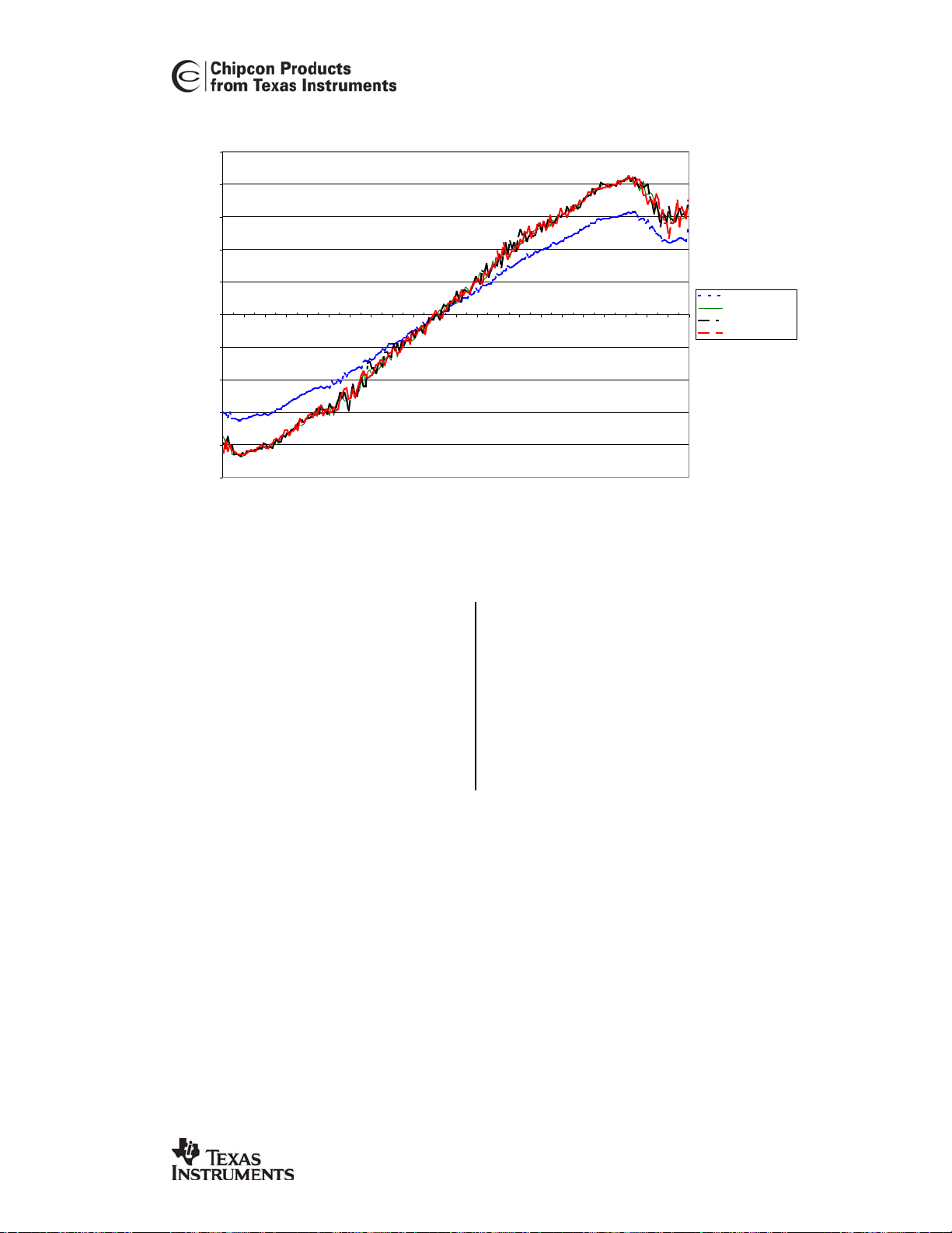
CC2400
100
80
60
40
20
0
-500 -450 -400 -350 -300 -250 -200 -150 -100 -50 0 50 100 150 200 250 300 350 400 450 500 550
AFC value
-20
-40
-60
-80
-100
Frequency offset [kHz]
Figure 21. AFC value vs. frequency offset
33 Linear IF and AGC Settings
CC2400
is based on a linear IF chain
where the signal amplification is done in
an analog VGA (variable gain amplifier).
The gain of the VGA is controlled by the
digital part of the IF-chain after the ADC
(Analog Digital Converter).
The AGC (Automatic Gain Control) loop
ensures that the ADC operates inside its
dynamic range by using an analog/digital
feedback loop.
The AGC characteristics are set through
the AGCCTRL, AGCTST0, AGCTST1 and
AGCTST2 registers.
Note that the RSSI function does not take
AGC settings into consideration if the AGC
settings are overridden.
AFC with settle = 8
AFC with settle = 4
AFC with settle = 2
AFC with settle = 1
SWRS042A Page 43 of 83

34 RSSI
CC2400
CC2400
has a built-in RSSI (Received
Signal Strength Indicator) giving a digital
value that can be read form the
RSSI.RSSI_VAL[7:0] register.
The RSSI reading provides a measure of
the signal power entering the RF input.
The scale is logarithmic, so that
RSSI_VAL provides a value in dB.
The number of samples that are used to
calculate the average signal amplitude is
controlled by the
RSSI.RSSI_FILT[1:0] register. The
RSSI filter length (averaging) can be done
over up to 8 symbols. This will determine
the response time of the RSSI.
The RSSI measurement can be referred to
the power at the RF input pins by using
the following equation:
P = RSSI_VAL + RSSI_OFFSET [dBm]
where the nominal value of
RSSI_OFFSET is –54dB. (If the gain in
the LNA/Mixer is changed from the default
settings, the offset is changed.)
A typical plot of the RSSI_VAL reading as
function of input power is shown in Figure
22 (for 1Mbps).
Note that the RSSI function does not take
AGC settings into consideration if the AGC
settings are overridden.
50
40
30
20
10
RSSI
-10
-20
-30
-40
-50
-60
0
0
2
-1
-116
-112
0
04-10
08
1
1
-
-
8-84-80
8
-96
-92
-
-76
8
6
-72
-
4-60
6
-
-56
Input level (dBm)
4-40-36
8
4
4
-
-52
-
-32
2
-28
-
4-20-16-12
4
-8
-
1M
250kb
10kb
0
Figure 22. Typical RSSI value vs. input power
SWRS042A Page 44 of 83

35 Carrier Sense
CC2400
The carrier sense signal is based on the
measured RSSI value and a
programmable threshold. The carriersense function can be used to simplify the
implementation of a CSMA (Carrier Sense
Multiple Access) medium access protocol.
Carrier sense threshold level is
programmed by
RSSI.RSSI_CS_THRES[5:0]. The
value of this register can be calculated in
the same way as described for
RSSI.RSSI_VAL in the previous section,
except that the unit is 4 dB instead of 1
dB. The default level (0x3C) corresponds
to a threshold of –70 dBm. A threshold of
0x09 corresponds to –18 dBm, and a
threshold of 0x37 corresponds to –90
dBm.
The carrier sense signal can be
multiplexed to the GIO1/GIO6 pin. The
CARRIER_SENSE_N signal is enabled by
setting IOCFG.GIO1_CFG[5:0] =
01010B (see Table 18).
36 Interfacing an External LNA or PA
CC2400
has two digital output pins, GIO1
and GIO6, which can be used to control
an external LNA or PA. The functionality of
these pins are controlled through the
IOCFG register.
The PA_EN, PA_EN_N, RX_PD, TX_PD
signals can be multiplexed to the
GIO1/GIO6 pin and used for controlling
the PA / LNA and one or more T/R
switches.
These two pins can also be used as two
general control signals, see Table 18.
For further information on attaching a PA,
please see page 54.
37 General Purpose / Test Output Control Pins
The two digital output pins, GIO1 and
GIO6, can be used as two general control
signals by writing to
IOCFG.GIO1_CFG[5:0] and
IOCFG.GIO6_CFG[5:0].
GIO1_CFG = 61 sets the pin low, and
GIO1_CFG = 62 sets the pin high.
GIO1_CFG /
GIO6_CFG
[decimal]
0 Reserved O Reserved
1 Reserved O Reserved
2 Reserved O Reserved
3 PA_EN O Active high PA enable signal
4 PA_EN_N O Active low PA enable signal
5 SYNC_RECEIVED O Set if a valid sync word has been received since last
6 PKT O Packet status signal See Figure 10, page 28.
7 Reserved I Reserved
8 Reserved O Reserved
9 Reserved O Reserved
Signal I/O Description
SWRS042A Page 45 of 83
This feature can be used to save I/O pins
on the microcontroller when the other
functions associated with these pins are
not used.
These two pins can also be used as a test
pin to monitor a lot of internal signals. This
is summarized in Table 18.
time RX was turned on
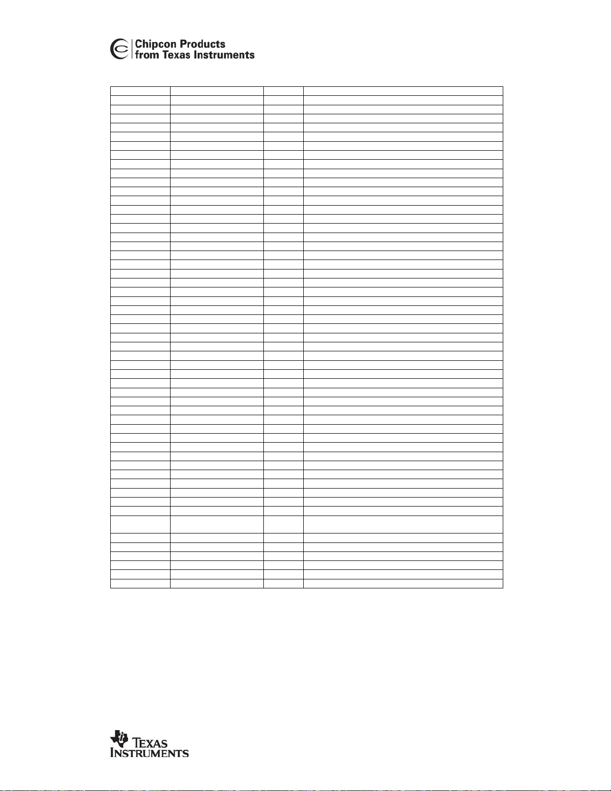
CC2400
10 CARRIER_SENSE_N O Carrier sense output (RSSI above threshold)
11 CRC_OK O CRC check OK after last byte read from FIFO
12 AGC_EN O AGC enable signal
13 FS_PD O Frequency synthesiser power down
14 RX_PD O RX power down
15 TX_PD O TX power down
16 Reserved O Reserved
17 Reserved O Reserved
18 Reserved O Reserved
19 Reserved O Reserved
20 Reserved O Reserved
21 Reserved O Reserved
22 PKT_ACTIVE O Packet reception active
23 MDM_TX_DIN O The TX data sent to modem
24 MDM_TX_DCLK O The TX clock used by modem
26 MDM_RX_DOUT O The RX data received by modem
26 MDM_RX_DCLK O The RX clock recovered by modem
27 MDM_RX_BIT_RAW O The un-synchronized RX data received by modem
28 Reserved O Reserved
29 MDM_BACKEND_EN O The Backend enable signal used by modem in RX
30 MDM_DEC_OVRFLW O Modem decimation overflow
31 AGC_CHANGE O Signal that toggles whenever AGC changes gain.
32 VGA_RESET_N O The VGA peak detectors' reset signal
33 CAL_RUNNING O VCO calibration in progress
34 SETTLING_RUNNING O Stepping CHP current after calibration
3 5 RXBPF_CAL_RUNNING O R X b an d -p a ss f il t er c al ib ra t io n ru n ni ng
36 VCO_CAL_START O VCO calibration start signal
37 RXBPF_CAL_START O RX band-pass filter start signal
38 FIFO_EMPTY O FIFO empty signal
39 FIFO_FULL O FIFO full signal
40 CLKEN_FS_DIG O Clock enable Frequency Synthesiser
41 CLKEN_RXBPF_CAL O Clock enable RX band-pass filter calibration
42 CLKEN_GR O Clock enable generic radio
43 XOSC16M_STABLE O Indicates that the Main crystal oscillator is stable
44 XOSC_16M_EN O 16 MHz XOSC enable signal
45 XOSC_16M O 16 MHz XOSC output from analog part
46 CLK_16M O 16 MHz clock from main clock tree
47 CLK_16M_MOD O 16 MHz modulator clock tree
48 CLK_8M16M_FSDIG O 8/16 MHz clock tree for fs_dig module
49 CLK_8M O 8 MHz clock tree derived from XOSC_16M
50 CLK_8M_DEMOD_AGC O 8 MHz clock tree for demodulator/AGC
51 Reserved O Reserved
52 Reserved O Reserved
53 FREF O Reference clock (4 MHz)
54 FPLL O Output clock of A/M-counter (4 MHz)
55 PD_F_COMP O Phase detector comparator output
56 WINDOW O Window signal to PD (Phase Detector)
57 LOCK_INSTANT O Window signal latched in PD (Phase Detector) by the
58 RESET_N_SYSTEM O Chip wide reset (except registers)
59 FIFO_FLUSH O FIFO flush signal
60 LOCK_STATUS O The top-level FS in lock status signal
61 ZERO O Output logic zero
62 ONE O Output logic one
63 HIGH_Z - Pin set as high-impedance output
Table 18. GIO1 / GIO6 signal select table
FREF clock
SWRS042A Page 46 of 83
⋅±=
38 Frequency Programming
CC2400
The operating frequency is set by
programming the frequency word in the
FSDIV configuration register.
The frequency word is 12 bits and is
located in FSDIV.FREQ[11:0].
Writing/reading FSDIV[11:0] will give
the frequency directly in MHz. (The bits
FSDIV.FREQ[11:10] are hardwired to
‘10’ giving a fixed offset of 2048.)
FSDIV should only be modified while the
CC2400
is in IDLE mode. Otherwise the
PLL may go out of lock as a calibration is
only performed when exiting IDLE mode.
38.1 Transmit mode
In transmit mode an I/Q direct
upconversion scheme is used (i.e. no
intermediate frequency for the modulated
baseband signal).
MDMTST0.TX_1MHZ_OFFSET_N=1 must
therefore be set during the chip
initialization sequence (ref. Figure 16).
When MDMTST0.TX_1MHZ_OFFSET_N=1
the transmit channel center frequency
(carrier frequency), f
directly by:
f
c
The two FSK modulation frequencies are
given by:
[] []
, in MHz is given
c
0:9FREQ0:11FREQ +== 2048
where f
f
MDMCTRL.MOD_DEV[6:0] and given by
(in kHz):
The default value is MOD_DEV = 64 giving
250 kHz deviation.
The TX_GAUSSIAN_FILTER bit in the
GRMDM register controls the Gaussian
shaping of the modulation signal. See also
page 38.
38.2 Receive mode
Low side LO injection is used, hence:
where, f
channel and f
Thus, in receive mode the frequency
generated by the frequency synthesizer,
f
frequency.
dev
is programmed with
dev
dev
RF
, must be programmed to be the LO
c
f
f
is the FSK frequency deviation.
f
LO
is the center frequency of the
= 1 MHz.
IF
= fc − f
0
= fc + f
1
= fRF − fIF
dev
dev
[]
0:6_9062.3 DEVMODf
39 Alternate TX IF setting
It is possible to configure
operate with an intermediate frequency of
1 MHz in transmit mode. It is not generally
recommended to do this, as the TX
spectrum will have higher spur content
than when using the direct up conversion
mode. Using an intermediate frequency of
CC2400
to
SWRS042A Page 47 of 83
1 MHz in TX has the advantage of much
lower RX/TX switching time because the
VCO operates at the same frequency in
RX and TX.
1 MHz IF in TX mode is enabled by setting
MDMTST0.TX_1MHZ_OFFSET_N=0.

[
(
40 VCO
CC2400
The VCO is completely integrated and
operates at 4800 – 4966 MHz. The VCO
frequency is divided by 2 to generate
frequencies in the desired band (24002483 MHz).
41 VCO Self-Calibration
The characteristics of the VCO will vary
with temperature, changes in supply
voltages, and the desired operating
frequency. In order to ensure reliable
42 Output Power Programming
The RF output power from the device is
programmable and is controlled by the
FREND.PA_LEVEL[2:0]
19 shows the relationship between the
register. Table
PA_LEVEL[2:0]
[binary]
000 -25 11
001 -15 12
010 -10 13
011 -7 14
100 -4.6 16
101 -2.8 17
110 -1.3 18
111 0 19
Output power
The VCO frequency is related to
FSDIV.FREQ[9:0] as follows:
]
)
VCO
operation the bias current and tuning
range of the VCO are automatically
calibrated every time the RX mode or TX
mode is enabled.
register value, output power and current
consumption.
RF frequency 2.45 GHz
[dBm]
+⋅=
Current
consumption,
typ. [mA]
0:920472 FREQf
Table 19. Output power settings and typical current consumption
SWRS042A Page 48 of 83
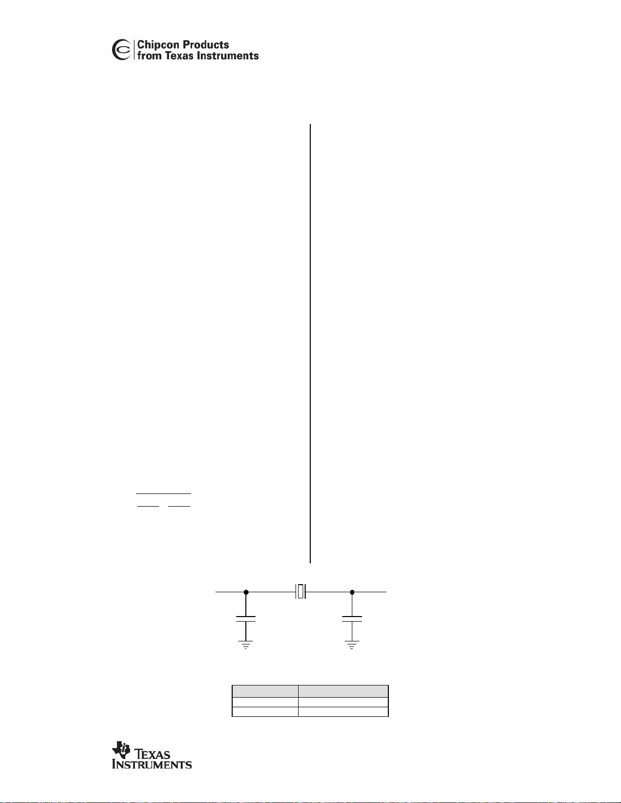
43 Crystal Oscillator
CC2400
An external clock signal or the internal
crystal oscillator can be used as main
frequency reference. The reference
frequency must be 16 MHz. Because the
crystal frequency is used as reference for
the data rate as well as other internal
signal processing functions, other
frequencies cannot be used.
If an external clock signal is used this
should be connected to XOSC16_Q1,
while XOSC16_Q2 should be left open. If
rail-to-rail (1.8V) square-wave signal is
used, the MAIN.XOSC16M_BYPASS bit
must be set. It is also possible to use a
sine-wave input. A voltage swing of 200
mV peak-to-peak is recommended in this
case.
Using the internal crystal oscillator, the
crystal must be connected between the
XOSC16_Q1 and XOSC16_Q2 pins. The
oscillator is designed for parallel mode
operation of the crystal. In addition,
loading capacitors (C5 and C6) for the
crystal are required. The loading capacitor
values depend on the total load
capacitance, C
The total load capacitance seen between
the crystal terminals should equal C
the crystal to oscillate at the specified
frequency.
C +
=
1
421
The parasitic capacitance is constituted by
pin input capacitance and PCB stray
capacitance. The total parasitic
capacitance is typically 5 pF.
, specified for the crystal.
L
for
L
1
+
CC
C
1
431
XOSC1 6_Q1 XOSC1 6_Q2
XOSC1 6_Q1 XOSC1 6_Q2
parasiticL
The crystal oscillator circuit is shown in
Figure 23. Typical component values for
different values of C
20. Note that these values will depend on
the PCB layout and the crystal used.
Determination of the values should be
done by measuring RF frequency on
several boards and adjusting the values of
the loading capacitors accordingly.
The crystal oscillator is amplitude
regulated. This means that a high current
is used to start up the oscillations. When
the amplitude builds up, the current is
reduced to what is necessary to maintain
a stable oscillation. This ensures a fast
start-up and keeps the drive level to a
minimum. The ESR of the crystal should
be within the specification in order to
ensure a reliable start-up (see the
Electrical Specifications section).
A small SMD crystal is used in the
reference design; note that the crystal
package strongly influences the price. In a
low-cost design, it may be preferable to
use a larger crystal package.
The required accuracy of the crystal is
determined by the receive filtering. Figure
19 shows how sensitivity varies with the
frequency offset between the transmitter
and the receiver. It is important to take the
total tolerance of the crystal into
consideration; this consists of the initial
tolerance, drift due to temperature and
aging.
are given in Table
L
XTA L
XTA LXTA L
C43 1C421
C43 1C421
Figure 23. Crystal oscillator circuit
Item CL= 16 pF
C421 22 pF
C431 22 pF
SWRS042A Page 49 of 83

Table 20. 16MHz crystal oscillator component values for CL=16pF
44 Input / Output Matching
CC2400
The RF input / output is differential (RF_N
and RF_P). In addition there is supply
switch output pin (TXRX_SWITCH) that
must have an external DC path to RF_N
and RF_P.
In RX mode the TXRX_SWITCH pin is at
ground and will bias the LNA. In TX mode
the TXRX_SWITCH pin is at supply rail
voltage and will properly bias the internal
PA.
The RF output and DC bias can be
achieved using different topologies.
45 Typical performance graphs
The following graphs show how some
important parameters vary with
temperature. These graphs show typical
performance as a function of temperature,
25
24
Application circuits are shown in Figure 3
and Figure 4. Component values are given
in Table 11.
If a single ended output is required (for a
single ended connector or a single ended
antenna), a balun should be used. The
balun can be realized using discrete
inductors and capacitors.
Using a differential antenna, no balun is
required.
and should be used as design guidance
only.
23
22
21
20
Current (mA)
19
18
17
16
15
-40-20 0 20406080
Temp (deg C)
Figure 24 Typical RX and TX current vs. temperature
SWRS042A Page 50 of 83
RX Current
TX Current

30
25
20
15
Current (uA)
10
5
0
-40-35-30-25-20-15-10-5 0 5 10152025 303540455055606570758085
Temp (deg C)
CC2400
Figure 25 Typical power-down current vs. temperature
5
4
3
2
1
0
-1
Power (dBm)
-2
-3
-4
-5
-6
-40-20 0 20406080
Temp (deg C)
Figure 26 Typical output power vs. temperature
SWRS042A Page 51 of 83
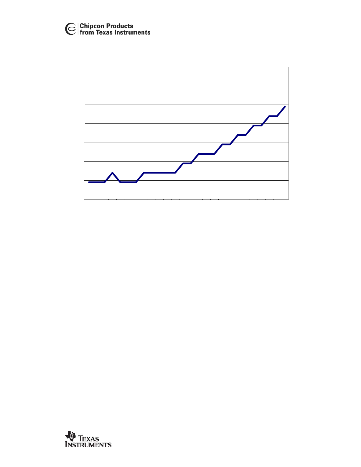
CC2400
-78
-80
-82
-84
-86
Sensitivity (dBm)
-88
-90
-92
-40 -15 10 35 60 85
Figure 27 Typical 1 Mbps sensitivity vs. temperature
Temperature (deg C)
SWRS042A Page 52 of 83

46 System Considerations and Guidelines
will be significantly rejected. This is
46.1 SRD regulations
International regulations and national laws
regulate the use of radio receivers and
transmitters. SRDs (Short Range Devices)
for license free operation are allowed to
operate in the 2.45 GHz bands worldwide.
The most important regulations are EN
300 440 and EN 300 328 (Europe), FCC
CFR47 part 15.247 and 15.249 (USA),
and ARIB STD-T66 (Japan).
The CC2400EM reference design
complies with EN 300 440. If frequency
hopping is to be used at 1 Mbps data rate,
GFSK should be selected to keep the
bandwidth below 1 MHz. The
complies with EN 300 440 class 2 if the
band spacing is 2 MHz or more. It
complies with EN 300 440 class 1 if the
channel and band spacing is 10 MHz or
more.
Please note that compliance with
regulations is dependent on complete
system performance. It is the customer’s
responsibility to ensure that the system
complies with regulations.
46.2 Frequency hopping and multi-
channel systems
The 2.400 – 2.4835 GHz band is shared
by many systems both in industrial, office
and home environment. It is therefore
recommended to use frequency hopping
spread spectrum (FHSS) or a multichannel protocol because the frequency
diversity makes the system more robust
with respect to interference from other
systems operating in the same frequency
band.
CC2400
is highly suited for FHSS or multichannel systems due to its agile frequency
synthesizer and effective communication
interface. Using the packet handling
support and data buffering is also
beneficial in such systems as these
features will significantly offload the host
controller.
Due to the low-IF I/Q receiver and the onchip complex filtering, the image channel
CC2400
SWRS042A Page 53 of 83
important for all 2.4GHz systems.
46.3 Data burst transmissions
The high maximum data rate of
opens up for burst transmissions. A low
average data rate link (say 10 kbps), can
be realized using a higher over-the-air
data rate. Buffering the data and
transmitting in bursts at high data rate (say
1 Mbps) will reduce the time in active
mode, and hence also reduce the average
current consumption significantly.
46.4 Continuous transmissions
In data streaming applications the
opens up for continuous transmissions at
1 Mbps effective data rate. A typical
application is digital audio systems. As the
modulation is done with an I/Q upconverter with LO I/Q-signals coming from
a closed loop PLL, there is no limitation in
the length of a transmission. (Open loop
modulation used in some transceivers
often prevents this kind of continuous data
streaming and reduces the effective data
rate.)
46.5 Crystal drift compensation
A unique feature in
frequency resolution using the
MDMCTRL.MOD_OFFSET[5:0]. This
feature can be used to compensate for
frequency offset and drift. The
compensation affects both the receiver
and the transmitter of the device being
compensated. I.e. the received signal of
the device will match the receiver’s
channel filter better. In the same way the
center frequency of the transmitted signal
will match the ‘external’ transmitter’s
signal.
Initial adjustment can be done using this
frequency programmability. This
eliminates the need for an expensive
TCXO and trimming in some applications.
The frequency offset between an ‘external’
transmitter and the receiver is measured
in the
an internal register
(FREQEST.RX_FREQ_OFFSET[7:0]).
CC2400
is the very fine
CC2400
and can be read back from
CC2400
CC2400
CC2400

The measured frequency offset can thus
be used to calibrate the frequency using
the ‘external’ transmitter as the reference.
See also page 42 (Automatic Frequency
Control). Figure 28 shows the
improvement that can be achieved.
This feature can also be used for
temperature compensation of the crystal if
the temperature drift curve is known and a
temperature sensor is included in the
system.
In less demanding applications, a crystal
with low temperature drift and low aging
could be used without further
compensation.
46.6 Spectrum efficient modulation
CC2400
also has the possibility to use
Gaussian shaped FSK (GFSK). This
spectrum-shaping feature improves
adjacent channel power (ACP) and
occupied bandwidth. In ‘true’ FSK systems
with abrupt frequency shifting, the
spectrum is inherently broad. By making
the frequency shift ‘softer’, the spectrum
can be made significantly narrower. Thus,
higher data rates can be transmitted in the
same bandwidth using GFSK.
46.7 Low latency systems
CC2400
latency is critical. Unbuffered mode should
be used for lowest latency, since it takes
time to fill the FIFO buffer. The total
latency over the RF link in unbuffered
mode is around 8 s.
provide very low RX-TX switching time, as
described on page 47.
is ideal for applications where
CC2400
can also
CC2400
46.8 Low cost syst ems
As the
channel performance without any external
filters, a very low cost system can be
made.
A differential antenna will eliminate the
need for a balun, and the DC biasing can
be achieved in the antenna topology, see
Figure 4.
A small SMD crystal is used in the
reference design; note that the crystal
package strongly influences the price. In a
low-cost design, it may be preferable to
use a larger crystal package.
46.9 Battery operated systems
In low power applications, the power down
mode should be used when not active.
Depending on the start-up time
requirement, the crystal oscillator core can
be powered during power down. See page
36 for information on how effective power
management can be implemented.
46.10 Increasing output power
In some applications it may be necessary
to extend the link range. Adding an
external power amplifier is the most
effective way of doing this.
The power amplifier should be inserted
between the antenna and the balun, and
two T/R switches are needed to
disconnect the PA in RX mode. See
Figure 29.
CC2400
provides 1 Mbps multi-
SWRS042A Page 54 of 83

t
CC2400
0
-10
-20
-30
-40
-50
Sensitivity (dBm)
-60
-70
-80
-90
-100
-350 -300 -250 -200 -150 -100 -50 0 50 100 150 200 250
Frequency offset from center (kHz)
Figure 28. Sensitivity vs. frequency offset with and without AFC
Antenna
Filter
PA
Balun
With mod_offset compensation
Without mod_offset compensa
CC2400
T/R switch
Figure 29. Block diagram of
CC2400
SWRS042A Page 55 of 83
T/R switch
usage with external power amplifier

47 PCB Layout Recommendations
CC2400
A four layer PCB is highly recommended.
The second layer of the PCB should be
the “ground-layer”.
The top layer should be used for signal
routing, and the open areas should be
filled with metallization connected to
ground using several vias.
The area under the chip is used for
grounding and must be connected closely
to the ground plane with several vias.
The ground pins should be connected to
ground as close as possible to the
package pin using individual vias. The decoupling capacitors should also be placed
as close as possible to the supply pins
and connected to the ground plane by
separate vias. Supply power filtering is
very important.
The external components should be as
small as possible (0402 is recommended)
and surface mount devices must be used.
Please note that components smaller than
those specified may have differing
characteristics.
Caution should be used when placing the
microcontroller in order to avoid
interference with the RF circuitry.
A Development Kit with a fully assembled
Evaluation Module is available. It is
strongly advised that this reference layout
is followed very closely in order to achieve
the best performance.
The schematic, BOM and layout Gerber
files for the reference designs are all
available from the Chipcon website.
SWRS042A Page 56 of 83

48 Antenna Considerations
CC2400
CC2400
can be used together with various
types of antennas. A differential antenna
like a dipole would be the easiest to
interface not needing a balun (balanced to
un-balanced transformation network).
The length of the λ/2-dipole antenna is
given by:
L = 14250 / f
where f is in MHz, giving the length in cm.
An antenna for 2450 MHz should be 5.8
cm. Each arm is therefore 2.9 cm.
Other commonly used antennas for shortrange communication are monopole,
helical and loop antennas. The singleended monopole and helical would require
a balun network between the differential
output and the antenna.
Monopole antennas are resonant
antennas with a length corresponding to
one quarter of the electrical wavelength
(λ/4). They are very easy to design and
can be implemented simply as a “piece of
wire” or even integrated into the PCB.
The length of the λ/4-monopole antenna is
given by:
L = 7125 / f
where f is in MHz, giving the length in cm.
An antenna for 2450 MHz should be 2.9
cm.
Non-resonant monopole antennas shorter
than λ/4 can also be used, but at the
expense of range. In size and cost critical
applications such an antenna may very
well be integrated into the PCB.
Enclosing the antenna in high dielectric
constant material reduces the overall size
of the antenna. Many vendors offer such
antennas intended for PCB mounting.
Helical antennas can be thought of as a
combination of a monopole and a loop
antenna. They are a good compromise in
size critical applications. But helical
antennas tend to be more difficult to
optimize than the simple monopole.
Loop antennas are easy to integrate into
the PCB, but are less effective due to
difficult impedance matching because of
their very low radiation resistance.
For low power applications the differential
antenna is recommended giving the best
range and because of its simplicity.
The antenna should be connected as
close as possible to the IC. If the antenna
is located away from the RF pins the
antenna should be matched to the feeding
transmission line (50 Ω).
SWRS042A Page 57 of 83
49 Configuration Registers
CC2400
The configuration of
CC2400
is done by
programming the 16-bit configuration
registers. The configuration data based on
selected system parameters are most
easily found by using the SmartRF
Studio
software. Complete descriptions of the
registers are given in the following tables.
After a RESET is programmed, all the
registers have default values as shown in
the tables.
Some registers are Strobe Command
Registers. Accessing these registers will
initiate the change of an internal state or
mode.
The FIFO is accessed as an 8-bit register.
Some registers contain signed values.
These are in two’s complement format. I.e.
for a 4-bit value, 0000 is 0, 1111 is –1,
1110 is –2, 1000 is -8 and 0111 is 7.
During the address transfer a status byte
is returned. This status byte is described
in Table 13 at page 23.
Overview of
Address
0x00 MAIN R/W
0x01 FSCTRL R/W
0x02 FSDIV R/W
0x03 MDMCTRL R/W
0x04 AGCCTRL R/W
0x05 FREND R/W
0x06 RSSI R/W
0x07 FREQEST R/W
0x08 IOCFG R/W
0x09
0x0A
0x0B FSMTC R/W
0x0C RESERVED R/W
0x0D MANAND R/W
0x0E FSMSTATE R/W
0x0F ADCTST R/W
0x10 RXBPFTST R/W
0x11 PAMTST R/W
0x12 LMTST R/W
0x13 MANOR R/W
0x14 MDMTST0 R/W
0x15 MDMTST1 R/W
0x16 DACTST R/W
0x17 AGCTST0 R/W
0x18 AGCTST1 R/W
0x19 AGCTST2 R/W
0x1A FSTST0 R/W
0x1B FSTST1 R/W
0x1C FSTST2 R/W
0x1D FSTST3 R/W
0x1E MANFIDL R
0x1F MANFIDH R
0x20 GRMDM R/W
0x21 GRDEC R/W
1
R/W - Read/write (control/status), R - Status only, S – Strobe command register (perform action upon access)
CC2400
Register name
‘s control registers
1
Description
Register Type
Main control register
Frequency synthesiser main control and status
Frequency synthesiser frequency division control
Modem main control and status
AGC main control and status
Analog front-end control
RSSI information
Received signal frequency offset estimation
I/O configuration register
Unused
Unused
Finite state machine time constants
Reserved register containing spare control and status bits
Manual signal AND-override register
Finite state machine information and breakpoint
ADC test register
Receiver bandpass filters test register
PA and transmit mixers test register
LNA and receive mixers test register
Manual signal OR-override register
Modem test register 0
Modem test register 1
DAC test register
AGC test register: various control and status.
AGC test register: AGC timeout.
AGC test register: AGC various parameters.
Test register: VCO array results and override.
Test register: VC DAC manual control. VCO current constant.
Test register:VCO current result and override.
Test register: Charge pump current etc.
Manufacturer ID, lower 16 bit
Manufacturer ID, upper 16 bit
Generic radio modem control
Generic radio decimation control and status
SWRS042A Page 58 of 83

CC2400
1
Register name
Address
0x22 PKTSTATUS R
0x23 INT R/W
0x24 Reserved R/W
0x25 Reserved R/W
0x26 Reserved R/W
0x27 Reserved R/W
0x28 Reserved R/W
0x29 Reserved R/W
0x2A Reserved R/W
0x2B Reserved R/W
0x2C SYNCL R/W
0x2D SYNCH R/W
...
0x60 SXOSCON S
0x61 SFSON S
0x62 SRX S
0x63 STX S
0x64 SRFOFF S
0x65 SXOSCOFF S
0x66 Reserved S
0x67 Reserved S
0x68 Reserved S
0x69 Reserved S
0x6A Reserved S
0x6B Reserved S
0x6C Reserved S
0x6D Reserved S
0x6E Reserved S
0x6F Reserved S
0x70 FIFOREG Special
Register Type
MAIN (0x00) - Main Control Register
Description
Packet mode status
Interrupt register
Synchronisation word, lower 16 bit.
Synchronisation word, upper 16 bit.
Command strobe register: Turn on XOSC.
Command strobe register: Start and calibrate FS and go from RX/TX to a wait
mode where the FS is running.
Command strobe register: Start RX.
Command strobe register: Start TX (turn on PA).
Command strobe register: Turn off RX/TX and FS.
Command strobe register: Turn off XOSC.
Used to write data to and read data from the 8-bit wide 32 bytes FIFO used to
buffer outgoing TX data and incoming RX data in buffered RF mode.
Bit Field Name Reset R/W Description
15 RESETN - R/W
14:10 - 0 W0
9 FS_FORCE_EN 0 R/W
8 RXN_TX 0 R/W
7:4 - 0 W0
3 - 0 R/W
2 - 0 R/W
1 XOSC16M_BYPASS 0 R/W
SWRS042A Page 59 of 83
Active low reset of entire circuit. Should be applied before doing
anything else.
Reserved, write as 0.
Forces the frequency synthesiser on (starts with a calibration).
The synthesiser can also be turned on in a number of other
ways.
Selects whether RX operation ('0') or TX operation ('1') is desired
when FS_FORCE_EN is used. RX or TX mode is usually
selected using the SRX and STX strobe commands (or RX and
TX pins).
Reserved, write as 0.
Reserved, write as 0.
Reserved, write as 0.
Bypasses the 16 MHz main crystal oscillator and uses a buffered
version of the signal on Q1 directly. Used for external clock only.

[
Bit Field Name Reset R/W Description
0 XOSC16M_EN 0 R/W
FSCTRL (0x01) - Frequency Synthesiser Control and Status
Bit Field Name Reset R/W Description
15:6 - 0 W0
5:4 LOCK_THRESHOLD[1:0] 1 R/W
3 CAL_DONE 0 R
2 CAL_RUNNING 0 R
1 LOCK_LENGTH 0 R/W
0 LOCK_STATUS 0 R
Forces the 16 MHz main crystal oscillator and the global bias on.
These modules can also be turned on in other ways.
Reserved, write as 0.
Number of consecutive reference clock periods with successful
sync windows required to indicate lock:
0: 64
1: 128
2: 256
3: 512
Calibration has been performed since the last time the FS was
turned on.
Calibration status, '1' when calibration in progress.
LOCK_WINDOW pulse width:
0: 2 CLK_PRE periods
1: 4 CLK_PRE periods
'1' when PLL is in lock, otherwise '0'.
CC2400
FSDIV (0x02) - Frequency Synthesiser Frequency Division Control
Bit Field Name Reset R/W Description
15:12 - 0 W0
11:10 FREQ[11:10] 2 R
9:0 FREQ[9:0] 353
R/W
Reserved, write as 0.
Read only.
Directly gives the right frequency in MHz when reading/writing
FREQ[11:0].
Frequency control word.
c
where f
is the channel centre frequency. See page 47 for a
c
description of how to program the channel for tansmit and
receive modes respectively.
Reading/writing FREQ[11:0] gives the right frequency in MHz.
The default value corresponds to f
][]
MDMCTRL (0x03) - Modem Control and Status
Bit Field Name Reset R/W Description
15:13 - 0 W0
12:7 MOD_OFFSET[5:0] 0 R/W
SWRS042A Page 60 of 83
Reserved, write as 0.
Modulator/Demodulator centre frequency in 15.625 kHz steps
(for the receiver the steps are relative to 1 MHz, for the
transmitter the steps are relative to 0MHz when
MDMTST0.TX_1MHZ_OFFSET_N=1).
Two's complement signed value. I.e. MOD_OFFSET=0x1F Î
centre frequency=1.48 MHz; MOD_OFFSET=0x20 Î centre
+==
0:92048 0:11 FREQFREQf
=2401MHz.
c
[MHz]
Bit Field Name Reset R/W Description
frequency=0.50 MHz.
6:0 MOD_DEV[6:0] 64 R/W
AGCCTRL (0x04) - AGC Control and Status
Bit Field Name Reset R/W Description
15:8 VGA_GAIN [7:0] 0XF7 R/W
7:4 - 0 W0
3 AGC_LOCKED 0 R
2 AGC_LOCK 0 R/W
1 AGC_SYNC_LOCK 0 R/W
0 VGA_GAIN_OE 0 R/W
Modulator frequency deviation in 3.9062 kHz steps (0-500 kHz).
Unsigned value. Reset value gives a deviation of 250 kHz.
When written, VGA manual gain override value; when read, the
currently used VGA gain setting.
Reserved, write as 0.
AGC lock status
Lock gain after maximum number of attempts.
Lock gain after sync word received and maximum number of
attempts. (As configured in AGCTST0.AGC_ATTEMPTS. Attempts
may be 0)
Use the
CC2400
VGA_GAIN value during RX instead of the AGC value.
FREND (0x05) – Front-end Control Register
Bit Field Name Reset R/W Description
15:4 - 0 W0
3 - 1 W1
2:0 PA_LEVEL[2:0] 7 R/W
Reserved, write as 0.
Reserved, write as 1.
PA output power level.
RSSI (0x06) - RSSI Status and Control Register
Bit Field Name Reset R/W Description
15:8 RSSI_VAL[7:0] - R
7:2 RSSI_CS_THRES[5:0] 0X3C R/W
1:0 RSSI_FILT[1:0] 2 R/W
Averaged RSSI estimate on a logarithmic scale in signed two’s
complement format. Unit is 1 dB.
Offset= -54dB, see also page 44.
Carrier sense signal threshold value in signed two’s complement
format. Unit is 4 dB.
The CS_ABOVE_THRESHOLD_N signal goes low when the
received signal is above this value.
The CS_ABOVE_THRESHOLD_N signal is available on the
GIO1 pin or in the status word returned during SPI address byte.
The reset value corresponds to a threshold of approx. -69 dBm.
RSSI averaging filter length:
0: 0 bits (no filtering)
1: 1 bit
2: 4 bits
3: 8 bits
SWRS042A Page 61 of 83
FREQEST (0x07) - Received frequency offset estimation
Bit Field Name Reset R/W Description
15:8 RX_FREQ_OFFSET[7:0] - R
7:0 - 0 W0
IOCFG (0x08) - I/O configuration register
Bit Field Name Reset R/W Description
15 - 0 W0
14:9 GIO6_CFG[5:0] 11 R/W
8:3 GIO1_CFG[5:0] 60 R/W
2:0 HSSD_SRC[2:0] 0 R/W
Estimate of the received signals centre frequency comparison to
the ideal 1 MHz centre frequency. Two's complement signed
value. See page 42.
Reserved, write as 0.
Reserved, write as 0.
Configuration of the GIO6 pin. See page 45 for options. The
reset value outputs the signal CRC_OK on pin GIO6.
How to use the GIO1 pin. See page 45 for options. The reset
value outputs the signal LOCK_STATUS on pin GIO1.
For test purposes only.
The HSSD (High Speed Serial Data) test module is used as
follows:
0: Off.
1: Output AGC status (gain setting / peak detector status /
accumulator value)
2: Output ADC I and Q values.
3: Output I/Q after digital down-mixing and channel filtering.
4: Output RX signal magnitude / frequency unfiltered (from
demodulator).
5: Output RX signal magnitude / frequency filtered (from
demodulator).
6: Output RSSI / RX frequency offset estimation
7: Input DAC values.
The HSSD test module requires that the FS is up and running as
it uses CLK_PRE (~150 MHZ) to produce its ~37.5 MHz data
clock and serialize its output words. Also, in order for HSSD to
function properly GRMDM.PIN_MODE must be set for HSSD.
CC2400
FSMTC (0x0B) - Finite state machine time constants
Bit Field Name Reset R/W Description
15:13 TC_RXON2AGCEN[2:0] 3 R/W
12:10 TC_PAON2SWITCH[2:0] 6 R/W
9:6 RES[9:6] 10 R/W
5:3 TC_TXEND2SWITCH[2:0] 2 R/W
SWRS042A Page 62 of 83
The time in 5 s steps from RX is turned on until the AGC is
enabled. This time constant must be large enough to allow the
RX chain to settle so that the AGC algorithm starts working on a
proper signal. The default value corresponds to 15 us.
The time in s from TX is started until the TX/RX switch allows
the TX signal to pass.
Reserved
The time in s from TX is stopped (for instance the last bit of the
packet is sent) until the RX/TX switch breaks the TX output and
the PKT signal is set.
CC2400
Bit Field Name Reset R/W Description
2:0 TC_TXEND2PAOFF[2:0] 4 R/W
RESERVED (0x0C) - Reserved register containing spare control and status bits
Bit Field Name Reset R/W Description
15:5 RES[15:5] 0 R/W
4:0 RES[4:0] 0 R/W
MANAND (0x0D) - Manual signal AND override register
Bit Field Name Reset R/W Description
15 VGA_RESET_N 1 R/W
14 LOCK_STATUS 1 R/W
13 BALUN_CTRL 1 R/W
12 RXTX 1 R/W
11 PRE_PD 1 R/W
10 PA_N_PD 1 R/W
9 PA_P_PD 1 R/W
8 DAC_LPF_PD 1 R/W
7 BIAS_PD 1 R/W
6 XOSC16M_PD 1 R/W
5 CHP_PD 1 R/W
4 FS_PD 1 R/W
2
For some important signals the value can be overridden manually by the MANAND and MANOVR registers. This is
done as follows for the hypothetical important signal
IS:
IS_USED = (IS * IS_AND_MASK) + IS_OR_MASK,
using Boolean notation.
The AND-mask and OR-mask for the important signals listed resides in the MANAND and MANOR registers,
respectively.
Examples:
•
Writing 0xFFFE to MANAND and 0x0000 to MANOR will force LNAMIX_PD=0 whereas all other signals will be
unaffected.
Writing 0xFFFF to MANAND and 0x0001 to MANOVR will force LNAMIX_PD=1 whereas all other signals will be
•
unaffected.
The time in s from TX is stopped until the TX chain is turned off
and the state machine goes to the next state. The PKT signal will
then go low. This value must be greater than
TC_TXEND2SWITCH[2:0].
Reserved
Reserved
2
Overrides VGA_RESET_N used to reset the peak detectors in
the VGA in the RX chain.
Must be set to 0 during chip initialization.
Overrides the LOCK_STATUS top-level signal that indicates
whether VCO lock is achieved or not.
Overrides the BALUN_CTRL signal that controls whether the PA
should receive its required external biasing (1) or not (0) by
controlling the RX/TX output switch.
Overrides the RXTX signal that controls whether the LO buffers
(0) or PA buffers (1) should be used.
Power down of prescaler.
Power down of PA (negative path).
Power down of PA (positive path). When PA_N_PD=1 and
PA_P_PD=1 the up-conversion mixers are in powerdown.
Power down of TX DACs.
Power down control of global bias generator + XOSC clock
buffer.
Power down control of 16 MHz XOSC core.
Power down control of charge pump.
Power down control of VCO, I/Q generator, LO buffers.
SWRS042A Page 63 of 83

Bit Field Name Reset R/W Description
3 ADC_PD 1 R/W
2 VGA_PD 1 R/W
1 RXBPF_PD 1 R/W
0 LNAMIX_PD 1 R/W
FSMSTATE (0x0E) - Finite state machine information and breakpoint
Bit Field Name Reset R/W Description
15:13 - 0 W0
12:8 FSM_STATE_BKPT[4:0] 0 R/W
7:5 - 0 W0
4:0 FSM_CUR_STATE[4:0] - R
ADCTST (0x0F) - ADC Test Register
Bit Field Name Reset R/W Description
15 - 0 W0
14:8 ADC_I[6:0] - R
7 - 0 W0
6:0 ADC_Q[6:0] - R
Power down control of the ADCs.
Power down control of the VGA.
Power down control of the band-pass receive filter.
Power down control of the LNA, down-conversion mixers and
front-end bias.
Reserved, write as 0.
FSM breakpoint state. State=0 means that breakpoints are
disabled.
Reserved, write as 0.
Gives the current state of the finite state machine.
Reserved, write as 0.
Read the current ADC I-branch value.
Reserved, write as 0.
Read the current ADC Q-branch value.
CC2400
RXBPFTST (0x10) - Receiver Band-pass Filters Test Register
Bit Field Name Reset R/W Description
15 - 0 W0
14 RXBPF_CAP_OE 0 R/W
13:7 RXBPF_CAP_O[6:0] 0 R/W
6:0 RXBPF_CAP_RES[6:0] - R
Reserved, write as 0.
RX band-pass filter capacitance calibration override enable.
RX band-pass filter capacitance calibration override value.
RX band-pass filter capacitance calibration result.
0 Minimum capacitance in the feedback.
1: Second smallest capacitance setting.
…
127: Maximum capacitance in the feedback.
SWRS042A Page 64 of 83

PAMTST (0x11) - PA and Transmit Mixers Test Regis ter
Bit Field Name Reset R/W Description
15:13 - 0 W0
12 VC_IN_TEST_EN 0 R/W
11 ATESTMOD_PD 1 W
10:8 ATESTMOD_MODE[2:0] 0 R/W
7 - 0 W0
6:5 TXMIX_CAP_ARRAY[1:0] 0 R/W
4:3 TXMIX_CURRENT[1:0] 0 R/W
2:0 PA_CURRENT[2:0] 3 R/W
Reserved, write as 0.
When ATESTMOD_MODE=7 this controls whether the ATEST1 in
is used to output the VC node voltage (0) or to control the VC
node voltage (1).
Power down of the analog test module.
When ATESTMOD_PD=0, the function of the analog test module
is as follows:
0: Outputs “I” (ATEST2) and “Q” (ATEST1) from RxMIX.
1: Inputs “I” (ATEST2) and “Q” (ATEST1) to BPF.
2: Outputs “I” (ATEST2) and “Q” (ATEST1) from VGA.
3: Inputs “I” (ATEST2) and “Q” (ATEST1) to ADC.
4: Outputs “I” (ATEST2) and “Q” (ATEST1) from LPF.
5: Inputs “I” (ATEST2) and “Q” (ATEST1) to TxMIX.
6: Outputs “P” (ATEST2) and “N” (ATEST1) from Prescaler.
7: Connects TX IF to RX IF and simultaneously the ATEST1 pin to the
internal VC node (see
Reserved, write as 0.
Selects varactor array settings in the transmit mixers.
Transmit mixers current:
0: 1.72 mA
1: 1.88 mA
2: 2.05 mA
3 2.21 mA
Programming of the PA current
0: -3 current adjustment
1: -2 current adjustment
2: -1 current adjustment
3: Nominal setting
4: +1 current adjustment
5: +2 current adjustment
6: +3 current adjustment
7: +4 current adjustment
CC2400
VC_IN_TEST_EN).
SWRS042A Page 65 of 83

LMTST (0x12) - LNA and receive mixers test register
Bit Field Name Reset R/W Description
15:14 - 0 W0
13 RXMIX_HGM 1 R/W
12:11 RXMIX_TAIL[1:0] 1 R/W
10:9 RXMIX_VCM[1:0] 1 R/W
8:7 RXMIX_CURRENT[1:0] 2 R/W
6:5 LNA_CAP_ARRAY[1:0] 1 R/W
4 LNA_LOWGAIN 0 R/W
3:2 LNA_GAIN[1:0] 0 R/W
1:0 LNA_CURRENT[1:0] 2 R/W
Reserved, write as 0.
Receiver mixers high gain mode enable.
Control of the receiver mixers output current.
0: 12 µA
1: 16 µA (Nominal)
2: 20 µA
3:24 µA
Controls VCM level in the mixer feedback loop
0: 8 µA mixer current
1: 12 µA mixer current (Nominal)
2: 16 µA mixer current
3: 20 µA mixer current
Must be set to 0 during chip initialisation.
Controls current in the mixer
0: 360 µA mixer current (x2)
1: 720 µA mixer current (x2)
2: 900 µA mixer current (x2) (Nominal)
3: 1260 µA mixer current (x2)
Selects varactor array setting in the LNA
0: OFF
1: 0.1pF (x2) (Nominal)
2: 0.2pF (x2)
3: 0.3pF (x2)
Selects low gain mode of the LNA
0: 19 dB (Nominal)
1: 7 dB
Controls current in the LNA gain compensation branch
0: OFF (Nominal)
1: 100 µA LNA current
2: 300 µA LNA current
3: 1000 µA LNA current
Controls main current in the LNA
0: 240 µA LNA current (x2)
1: 480 µA LNA current (x2)
2: 640 µA LNA current (x2) (Nominal)
3: 1280 µA LNA current (x2)
CC2400
SWRS042A Page 66 of 83

MANOR (0x13) - Manual signal OR override register3
Bit Field Name Reset R/W Description
15 VGA_RESET_N 0 R/W
14 LOCK_STATUS 0 R/W
13 BALUN_CTRL 0 R/W
12 RXTX 0 R/W
11 PRE_PD 0 R/W
10 PA_N_PD 0 R/W
9 PA_P_PD 0 R/W
8 DAC_LPF_PD 0 R/W
7 BIAS_PD 0 R/W
6 XOSC16M_PD 0 R/W
5 CHP_PD 0 R/W
4 FS_PD 0 R/W
3 ADC_PD 0 R/W
2 VGA_PD 0 R/W
1 RXBPF_PD 0 R/W
0 LNAMIX_PD 0 R/W
Overrides VGA_RESET_N used to reset the peak detectors in
the VGA in the RX chain.
Overrides the LOCK_STATUS top-level signal that indicates
whether VCO lock is achieved or not.
Overrides the BALUN_CTRL signal that controls whether the PA
should receive its required external biasing (1) or not (0) by
controlling the RX/TX output switch.
Overrides the RXTX signal that controls whether the LO buffers
(0) or PA buffers (1) should be used.
Power down of prescaler.
Power down of PA (negative path).
Power down of PA (positive path). When
PA_P_PD=1 the up-conversion mixers are in power down.
Power down of TX DACs.
Power down control of global bias generator + XOSC clock
buffer.
Power down control of 16 MHz XOSC core.
Power down control of charge pump.
Power down control of VCO, I/Q generator, LO buffers.
Power down control of the ADCs.
Power down control of the VGA.
Power down control of complex band-pass receive filter.
Power down control of LNA, down-conversion mixers and frontend bias.
CC2400
PA_N_PD=1 and
MDMTST0 (0x14) - Modem Test Register 0
Bit Field Name Reset R/W Description
15:14 - 0 W0
13 TX_PRNG 0 R/W
12 TX_1MHZ_OFFSET_N 0 R/W
11 INVERT_DATA 0 R/W
10 AFC_ADJUST_ON_PACKET 0 R/W
Reserved, write as 0.
When set, the transmitted data is taken from a 10-bit PRNG
instead of from the DIO pin in un-buffered mode or from the
FIFO in buffered mode.
Determines TX IF frequency:
0: 1 MHz (Not used)
1: 0 MHz (During initialization this bit must be set to a logical ’1’.)
When this bit is set the data are inverted (internally) before
transmission, and inverted after reception.
When this bit is set to '1', modem parameters are adjusted for
slow tracking of the received signal as opposed to quick
acquisition when a packet is received in RX.
• 3 See footnote for MANAND register (address 0x0D) for description of the use of this register.
SWRS042A Page 67 of 83

Bit Field Name Reset R/W Description
9:8 AFC_SETTLING[1:0] 3 R/W
7:0 AFC_DELTA[7:0] 75 R/W
MDMTST1 (0x15) - Modem Test Register 1
Bit Field Name Reset R/W Description
15:7 - 0 W0
6:0 BSYNC_THRESHOLD[6:0] 75 R/W
Controls how many max-min pairs that are used to compute the
output.
00: 1 pair
01: 2 pairs
10: 4 pairs
11: 8 pairs
Programmable level used in AFC-algorithm that indicates the
expected frequency deviation of the received signal. See page
42 for further details.
Reserved, write as 0.
Threshold value used in clock recovery algorithm. Sets the level
for when re-synchronization takes place.
CC2400
DACTST (0x16) - DAC Test Register
Bit Field Name
15 - 0 W0
14:12 DAC_SRC[2:0] 0 R/W
11:6 DAC_I_O[5:0] 0 R/W
5:0 DAC_Q_O[5:0] 0 R/W
Reset
R/W Description
Reserved, write as 0.
The TX DACs data source is selected by DAC_SRC according
to:
0: Normal operation (from modulator).
1: The DAC_I_O and DAC_Q_O override values below.
2: From ADC
3: I/Q after digital down-mixing and channel filtering.
4: Full-spectrum White Noise (from PRNG.)
5: RX signal magnitude / frequency filtered (from demodulator).
6: RSSI / RX frequency offset estimation.
7: HSSD module.
This feature will often require the DACs to be manually turned on
in MANOVR and PAMTST.ATESTMOD_MODE=4.
I-branch DAC override value.
Q-branch DAC override value.
SWRS042A Page 68 of 83
AGCTST0 (0x17) - AGC Test Register 0
Bit Field Name Reset R/W Description
15:13 AGC_SETTLE_BLANK_DN[2:
0]
12:11 AGC_WIN_SIZE[1:0] 2 R/W
10:7 AGC_SETTLE_PEAK[3:0] 2 R/W
6:3 AGC_SETTLE_ADC[3:0] 2 R/W
2:0 AGC_ATTEMPTS[2:0] 0 R/W
AGCTST1 (0x18) - AGC Test Register 1
Bit Field Name Reset R/W Description
15 - 0 W0
14 AGC_VAR_GAIN_SAT 1 R/W
13:11 AGC_SETTLE_BLANK_UP
[2:0]
10 PEAKDET_CUR_BOOST 0 R/W
9:6 AGC_MULT_SLOW[3:0] 0 R/W
5:2 AGC_SETTLE_FIXED[3:0] 4 R/W
1:0 AGC_SETTLE_VAR[1:0] 0 R/W
4 R/W
0 R/W
AGC blanking enable/limit for negative gain changes.
0: Disabled
1-7: Duration of blanking signal in 8 MHz clock cycles.
AGC window size.
AGC peak detectors settling period.
AGC ADC settling period.
The maximum number of attempts to set the gain.
Reserved, write as 0.
Chooses the gain reduction upon saturation of the variable
gain stage:
0: -1/-3 gain steps
1: -3/-5 gain steps
AGC blanking enable/limit for positive gain changes.
0: Disabled
1-7: Duration of blanking signal in 8 MHz clock cycles.
Doubles the bias current in the peak-detectors in-between the
VGA stages when set.
AGC timing multiplier, slow mode.
AGC settling period, fixed gain step.
AGC settling period, variable gain step.
CC2400
AGCTST2 (0x19) - AGC Test Register 1
Bit Field Name Reset R/W Description
15:14 - 0 W0
13:12 AGC_BACKEND_BLANKING
[1:0]
11:9 AGC_ADJUST_M3DB[2:0] 0 R/W
8:6 AGC_ADJUST_M1DB[2:0] 0 R/W
5:3 AGC_ADJUST_P3DB[2:0] 0 R/W
2:0 AGC_ADJUST_P1DB[2:0] 0 R/W
0 R/W
Reserved, write as 0.
AGC blanking makes sure that the modem locks its bit
synchronization and centre frequency estimator when the AGC
changes the gain.
0: Disabled
1-3: Fixed/variable enable
AGC parameter -3 dB.
AGC parameter -1 dB.
AGC parameter +3 dB.
AGC parameter +1 dB.
SWRS042A Page 69 of 83

FSTST0 (0x1A) - Frequency Synthesiser Test Register 0
Bit Field Name Reset R/W Description
15:14 RXMIXBUF_CUR[1:0] 2 R/W
13:12 TXMIXBUF_CUR[1:0] 2 R/W
11 VCO_ARRAY_SETTLE_LONG 0 R/W
10 VCO_ARRAY_OE 0 R/W
9:5 VCO_ARRAY_O[4:0] 16 R/W
4:0 VCO_ARRAY_RES[4:0] - R
FSTST1 (0x1B) - Frequency Synthesiser Test Register 1
RX mixer buffer bias current.
0: 690uA
1: 980uA
2: 1.16mA (nominal)
3: 1.44mA
TX mixer buffer bias current.
0: 690uA
1: 980uA
2: 1.16mA (nominal)
3: 1.44mA
When '1' this control bit doubles the time allowed for VCO
settling during FS calibration.
VCO array manual override enable.
VCO array override value.
The resulting VCO array setting from the last calibration.
CC2400
Bit Field Name Reset R/W Description
15 RXBPF_LOCUR 0 R/W
14 RXBPF_MIDCUR 0 R/W
13:10 VCO_CURRENT_REF[3:0] 4 R/W
9:4 VCO_CURRENT_K[5:0] 0 R/W
3 VC_DAC_EN 0 R/W
2:0 VC_DAC_VAL[2:0] 2 R/W
Controls reference bias current to RX band-pass filters:
0: 4 uA (nominal)
1: 3 uA
Controls reference bias current to RX band-pass filters:
0: 4 uA (nominal)
1: 3.5 uA
The value of the reference current calibrated against during VCO
calibration.
VCO current calibration constant (override value current B when
FSTST2.VCO_CURRENT_OE=1).
Controls the source of the VCO control voltage in normal
operation (PAMTST.VC_IN_TEST_EN=0):
0: Loop filter (closed loop PLL)
1: VC DAC (open loop PLL)
VC DAC output value. (The value of the reference voltage used
during VCO calibration.)
SWRS042A Page 70 of 83

FSTST2 (0x1C) - Frequency Synthesiser Test Register 2
Bit Field Name Reset R/W Description
15 - 0 W0
14:13 VCO_CURCAL_SPEED[1:0] 0 R/W
12 VCO_CURRENT_OE 0 R/W
11:6 VCO_CURRENT_O[5:0] 24 R/W
5:0 VCO_CURRENT_RES[5:0] - R
FSTST3 (0x1D) - Frequency Synthesiser Test Register 3
Bit Field Name Reset R/W Description
15:14 - 0 W0
13 CHP_TEST_UP 0 R/W
12 CHP_TEST_DN 0 R/W
11 CHP_DISABLE 0 R/W
10 PD_DELAY 0 R/W
9:8 CHP_STEP_PERIOD[1:0] 2 R/W
7:4 STOP_CHP_CURRENT[3:0] 13 R/W
3:0 START_CHP_CURRENT
[3:0]
13 R/W
Reserved, write as 0.
VCO current calibration speed:
0: Normal
1: Undefined
2: Half speed
3: Undefined.
VCO current manual override enable.
VCO current override value (current A).
The resulting VCO current setting from last calibration.
Reserved, write as 0.
When CHP_DISABLE
When CHP_DISABLE
current.
Set to disable charge pump during VCO calibration.
Selects short or long reset delay in phase detector:
0: Short reset delay
1: Long reset delay
The charge pump current value step period:
0: 0.25 us
1: 0.5 us
2: 1 us
3: 4 us
The charge pump current to stop at after the current is stepped
down from START_CHP_CURRENT after VCO calibration is
complete. The current is stepped down periodically with intervals
as defined in CHP_STEP_PERIOD.
The charge pump current to start with after VCO calibration is
complete. The current is then stepped down periodically to the
value STOP_CHP_CURRENT with intervals as defined in
CHP_STEP_PERIOD
CC2400
=1 forces the CHP to output "up" current.
=1 forces the CHP to output "down"
.
SWRS042A Page 71 of 83

MANFIDL (0x1E) - Manufacturer ID, Lower 16 Bit
Bit Field Name Reset R/W Description
15:12 PARTNUM[3:0] 1 R
11:0 MANFID[11:0] 0X33D R
MANFIDH (0x1F) - Manufacturer ID, Upper 16 Bit
Bit Field Name Reset R/W Description
15:12 VERSION[3:0] 0 R
11:0 PARTNUM[15:4] 0 R
GRMDM (0x20) - Generic Radio Modem Control and Status
Bit Field Name Reset R/W Description
15 - 0 W0
14:13 SYNC_ERRBITS_ALLOWED
[1:0]
12:11 PIN_MODE[1:0] 1 R/W
10 PACKET_MODE 1 R/W
9:7 PRE_BYTES[2:0] 3 R/W
6:5 SYNC_WORD_SIZE[1:0] 3 R/W
4 CRC_ON 1 R/W
0 R/W
The device part number.
Gives the JEDEC manufacturer ID. The actual manufacturer ID
can be found in MANIFID[7:1], the number of continuation
bytes in MANFID[11:8] and MANFID[0]
Chipcon's JEDEC manufacturer ID is 0x7F 0x7F 0x7F 0x9E
(0x9E preceded by three continuation bytes.)
Chip version number.
The device part number.
Reserved, write as 0.
Sync word detection occurs when the number of bits in the sync
word correlator different from that specified by the SYNC
registers is equal to or lower than SYNC_ERRBITS_ALLOWED.
Selects between un-buffered mode, buffered mode or test mode.
The pin configuration is set according to Table 15.
0: Un-buffered mode
1: Buffered mode
2: HSSD test mode
3: Unused
When this bit is set the packet mode is enabled. The pin
configuration is set according to Table 15.
In TX, this enables preamble generation, sync word, and CRC
appending (if enabled by CRC_ON) in the buffered mode.
In RX, this enables sync word detection in buffered and un-
buffered modes, and CRC verification (if enabled by CRC_ON) in
buffered mode.
The number of preamble bytes ("01010101") to be sent in packet
mode:
000: 0 001: 1 010: 2 011: 4
100: 8 101: 16 110: 32 111: Infinitely on
The size of the packet mode sync word sent in TX and correlated
against in RX:
00: The 8 MSB bits of SYNC_WORD.
01: The 16 MSB bits of SYNC_WORD.
10: The 24 MSB bits of SYNC_WORD.
11: The 32 MSB bits of SYNC_WORD.
In packet mode a CRC is calculated and is transmitted after the
data in TX, and a CRC is calculated during reception in RX.
CC2400
CC2400
has part number 0x001.
CC2400
has part number 0x001.
=1.
SWRS042A Page 72 of 83

Bit Field Name Reset R/W Description
3:2 DATA_FORMAT[1:0] 0 R/W
1 MODULATION_FORMAT 0 R/W
0 TX_GAUSSIAN_FILTER 1 R/W
GRDEC (0x21) - Generic Radio Decimation Control and Status
Bit Field Name Reset R/W Description
15:13 - 0 W0
12 IND_SATURATION - R
11:10 DEC_SHIFT[1:0] 0 R/W
9:8 CHANNEL_DEC[1:0] 0 R/W
7:0 DEC_VAL[7:0] 0 R/W
PKTSTATUS (0x22) - Packet Mode Status
Selects line-coding format used during RX and TX operations.
00: NRZ
01: Manchester
10: 8/10 line-coding (Not applied to preambles or sync words)
11: Reserved
Modulation format of modem:
0: FSK/GFSK
1: Reserved
When this bit is set the data sent in TX is Gaussian filtered
before transmission enabling GFSK
Reserved, write as 0.
Signal indicates whether the accumulate-and-dump decimation
filters have saturated at some point since the last read. If
saturation occurs the DEC_SHIFT can be adjusted. The status
flag is cleared when reading the GRDEC register.
Controls extra shifts in decimation, for extra precision.
Decimation shift value:
2: -2
3: -1
0: 0
1: 1
Selects channel filter bandwidth.
00: 1 MHz (used for 1Mbps and 250 kbps datarates)
01: 500 kHz (used for 10 kbps data rate)
01: 250 kHz
11: 125 kHz
In combination with CHANNEL_DEC[1:0], DEC_VAL[7:0] is
used to program the data rate. See page 40 for a description.
CC2400
Bit Field Name Reset R/W Description
15:11 - 0 W0
10 SYNC_WORD_RECEIVED 0 R
9 CRC_OK - R
8 - 0 R
7:0 - - R
Reserved, write as 0.
Indicates that the currently configured sync word has been
received since RX was turned on.
Indicates that the two next bytes available to be read from the
FIFO equal the CRC16 calculated over the bytes already read
from the FIFO.
Reserved for future use.
Reserved for future use.
SWRS042A Page 73 of 83

INT (0x23) - Interrupt Register
Bit Field Name Reset R/W Description
15:8 - 0 W0
7 - 0 R/W
6 PKT_POLARITY 0 R/W
5 FIFO_POLARITY 0 R/W
4:0 FIFO_THRESHOLD[4:0] 30 R/W
Reserved (0x24) – Reserved regiser
Bit Field Name Reset R/W Description
15:14 RES[15:14] 0 W0
13:10 RES[13:10] 8 R/W
9:7 RES[9:7] 0 R/W
6:0 RES[6:0] 80 R/W
Reserved (0x25) – Reserved register
Reserved, write as 0.
Reserved.
Polarity of the PKT signal.
Polarity of the FIFO signal. See Figure 10 for details.
The FIFO pin signals that the 32 bytes data FIFO is near empty
in TX or near full in RX. The threshold is used as follows:
# bytes in FIFO >= FIFO_THRESHOLD in RX
# bytes in FIFO <= 32 - FIFO_THRESHOLD in TX.
Reserved for future use.
Reserved for future use.
Reserved for future use.
Reserved for future use.
CC2400
Bit Field Name Reset R/W Description
15:12 RES[15:12] 0 W0
11:0 RES[11:0] 0 R/W
Reserved for future use.
Reserved for future use.
Reserved (0x26) – Reserved register
Bit Field Name Reset R/W Description
15:10 RES[15:10] 8 R/W
9:0 RES[9:0] 0 R/W
Reserved for future use.
Reserved for future use.
Reserved (0x27) – Reserved register
Bit Field Name Reset R/W Description
15:8 RES[15:8] - R
7:3 RES[7:3] 0 R/W
2:0 RES[2:0] 6 R/W
Reserved for future use.
Reserved for future use.
Reserved for future use.
Reserved (0x28) – Reserved register
Bit Field Name Reset R/W Description
15 RES[15] 0 R/W
14:13 RES[14:13] 2 R/W
12:7 RES[12:7] 63 R/W
Reserved for future use.
Reserved for future use.
Reserved for future use.
SWRS042A Page 74 of 83

Bit Field Name Reset R/W Description
6:0 RES[6:0] 0 R/W
Reserved (0x29) – Reserved Register
Bit Field Name Reset R/W Description
15:8 RES[15:8] 0 W0
7:3 RES[7:3] 0 R/W
2:0 RES[2:0] 3 R/W
Reserved (0x2A) – Reserved Register
Bit Field Name Reset R/W Description
15:11 RES[15:11] 0 W0
10 RES[10] 0 R/W
9:0 RES[9:0] 512 R/W
Reserved (0x2B) – Reserved register
Reserved for future use.
Reserved for future use.
Reserved for future use.
Reserved for future use.
Reserved for future use.
Reserved for future use.
Reserved for future use.
CC2400
Bit Field Name Reset R/W Description
15:14 RES[15:14] 0 W0
13 RES[13] - R/W
12 RES[12] - R
11:0 RES[11:0] 1953 R
Reserved for future use.
Reserved for future use.
Reserved for future use.
Reserved for future use.
SYNCL (0x2C) - Sync Word, Lower 16 Bit
Bit Field Name Reset R/W Description
15:0 SYNCWORD[15:0] 0XDA26 R/W
Synchronisation word, lower 16 bit.
The default synchronization word of
good DC, autocorrelation, and bit-run properties for all
synchronization word lengths.
SYNCH (0x2D) - Sync Word, Upper 16 Bit
Bit Field Name Reset R/W Description
15:0 SYNCWORD[31:16] 0XD391 R/W
Synchronisation word, upper 16 bit.
0XD391DA26 has very
SWRS042A Page 75 of 83

50 Package Description (QFN48)
CC2400
Note: The figure is an illustration only and not to scale.
A A1 b D E D1 E1 e L L1 L2
QFN 48 Min
The overall package height is 0.9 +/ 0.1 mm.
All dimensions in mm
Max
0.8
1.0
0.203
The package is compliant to JEDEC standard MO-220.
Quad Flat Pack - No Lead Package (QFN)
0.18
0.25
0.30
7.0 7.0
SWRS042A Page 76 of 83
5.04
5.24
5.04
5.24
0.5
0.43
0.53
0.63
0.1
0.30
0.40
0.50
51 Recommended layout for package (QFN48)
CC2400
Note: The figure is an illustration only and not to scale. There are nine 14 mil diameter via
holes distributed symmetrically in the ground pad under the package. See also the
CC2400EM reference design.
52 Package Thermal Properties
Thermal resistance
Air velocity [m/s] 0
Rth,j-a [K/W] 25.6
53 Soldering Information
Recommended soldering profile for both standard leaded packages and Pb-free packages is
according to IPC/JEDEC J-STD-020B, July 2002.
SWRS042A Page 77 of 83

CC2400
54 IC marking
Note: Please submit the entire marking information when contacting Chipcon technical
support about chip-related issues, not just the date code.
Example of QFN 48 standard leaded assembly
0440XAA
0440 is assembly year and week no.
XAA is lot code
SWRS042A Page 78 of 83

Example of QFN 48 RoHS compliant Pb-free ass em bly
A440XAA
CC2400
A is to identify RoHS compliant Pb-free assembly
4 is to identify year 2004
40 is week no
XAA is lot code
SWRS042A Page 79 of 83
55 Plastic Tube Specification
QFN 7x7 mm antistatic tube.
Package Tube Width Tube Height Tube Length Units per Tube
QFN 48
8.5 ± 0.2 mm
56 Carrier Tape and Reel Specification
Carrier tape and reel is in accordance with EIA Specification 481.
Package Tape Width Component
QFN 48 16 mm 12 mm 4 mm 13 inch 4000
57 Ordering Information
Tube Specification
2.2 +0.2/-0.1
mm
Tape and Reel Specification
Pitch
315 ± 1.25 mm
Hole
Pitch
Reel
Diameter
43
Units per Reel
CC2400
1170
1096
1139
1140
10031 CC2400DK CC2400DK Development kit
10041
1097
1162
MOQ = Minimum Order Quantity
T&R = tape and reel
Ordering part number
CC2400-STB1 CC2400, QFN48 package, standard leaded assembly, tubes with
CC2400-STR1 CC2400, QFN48 package, standard leaded assembly, T&R with
CC2400-RTB1 CC2400, QFN48 package, RoHS compliant Pb-free assembly,
CC2400-RTR1 CC2400, QFN48 package, RoHS compliant Pb-free assembly,with
CC2400DBK
CC2400SK
CC2400SK RoHS
Description MOQ
43 pcs per tube, 2.4 GHz RF transceiver.
4000 pcs per reel, 2.4 GHz RF transceiver.
tubes with 43 pcs per tube, 2.4 GHz RF transceiver.
4000/T&R per reel, 2.4 GHz RF transceiver.
CC2400DBK, Demonstration Board Kit
CC2400 QFN48 package, standard leaded assembly, (5 pcs.)
CC2400 QFN48 package, RoHS compliant Pb-free assembly, 5
pcs.
43
4,000
43
4,000
1
1
1
1
SWRS042A Page 80 of 83

58 General Information
58.1 Document History
Revision Date Description/Changes
1.5 2006-03-20 Removed QLP information
1.4 2006-01-16 Address information and ordering information have
1.3 2004-10-20 Various clarifications.
1.2 2004-02-05 Various clarifications.
1.1 2003-10-02 Removed 32 kHz oscillator.
1.0 2003-09-10 Initial release.
been updated.
Added recommended PCB footprint.
Added package height.
Added radio control state diagram with state ID
numbers.
Added information about EN 300 328 and EN 300
440.
Added AFC, RSSI settling time and 20 dB bandwidth
to electrical specifications.
Electrical specifications updated.
Bit 5 of the
reserved; see Errata Note 003 for details.
RSSI and carrier sense value calculation clarified and
corrected.
Added graphs showing typical current consumption,
sensitivity and output power as function of
temperature
Clarified packet handling and data buffering sections.
Description of the
Added example calculation to AFC description.
Updated ordering information with RoHS-compliant
Pb-free versions.
“CRC-16” replaced with “CRC”.
Reorganized electrical specification section.
Added chapter numbering.
Added QFN 48 package description.
Added IC marking description.
RSSI value calculation corrected.
Single-ended operation of the chip has been
removed.
Corrected value of DEC_VAL for 250 kbps data rate.
Added information that the core supply cannot be
switched off while I/O supply is still on.
Electrical specification updated.
Selectivity in-band is now measured using a FSK
modulated interferer.
Added note that choice of crystal package strongly
affects price.
Added section about low-latency systems.
Added graph of sensitivity vs. frequency offset.
Added plot of modulated spectrum.
Added more information about AFC.
Added information about using an external PA.
Operating conditions put into separate table.
Added L71 to application circuit.
Modified component names in application circuit to
match reference design.
Corrected E2 and D2 package dimensions.
Minor corrections and editorial changes.
Added recommendation on length of preamble when
using GFSK.
Added Manchester data encoding.
CC2400
STATUS register has been set as
FSMTC register corrected.
SWRS042A Page 81 of 83
CC2400
58.2 Product Status Definitions
Data Sheet Identification Product Status Definition
Advance Information Planned or Under
Preliminary Engineering Samples
No Identification Noted Full Production This data sheet contains the final specifications.
Obsolete Not In Production This data sheet contains specifications on a product
Development
and First Production
58.3 Disclaimer
Chipcon AS believes the information contained herein is correct and accurate at the time of this printing. However,
Chipcon AS reserves the right to make changes to this product without notice. Chipcon AS does not assume any
responsibility for the use of the described product; neither does it convey any license under its patent rights, or the
rights of others. The latest updates are available at the Chipcon website or by contacting Chipcon directly.
As far as possible, major changes of product specifications and functionality, will be stated in product specific Errata
Notes published at the Chipcon website. Customers are encouraged to sign up to the Developers Newsletter for the
most recent updates on products and support tools.
When a product is discontinued this will be done according to Chipcon’s procedure for obsolete products as
described in Chipcon’s Quality Manual. This includes informing about last-time-buy options. The Quality Manual can
be downloaded from Chipcon’s website.
Compliance with regulations is dependent on complete system performance. It is the customer’s responsibility to
ensure that the system complies with regulations.
This data sheet contains the design specifications for
product development. Specifications may change in
any manner without notice.
This data sheet contains preliminary data, and
supplementary data will be published at a later date.
Chipcon reserves the right to make changes at any
time without notice in order to improve design and
supply the best possible product.
Chipcon reserves the right to make changes at any
time without notice in order to improve design and
supply the best possible product.
that has been discontinued by Chipcon. The data
sheet is printed for reference information only.
58.4 Trademarks
SmartRF is a registered trademark of Chipcon AS. SmartRF is Chipcon's RF technology platform with
RF library cells, modules and design expertise. Based on SmartRF
standard component RF circuits as well as full custom ASICs based on customer requirements and this
technology.
All other trademarks, registered trademarks and product names are the sole property of their respective
owners.
technology Chipcon develops
58.5 Life Support Policy
This Chipcon product is not designed for use in life support appliances, devices, or other systems where
malfunction can reasonably be expected to result in significant personal injury to the user, or as a critical
component in any life support device or system whose failure to perform can be reasonably expected to
cause the failure of the life support device or system, or to affect its safety or effectiveness. Chipcon AS
customers using or selling these products for use in such applications do so at their own risk and agree to
fully indemnify Chipcon AS for any damages resulting from any improper use or sale.
© 2003, 2004, 2005, 2006 Chipcon AS. All rights reserved.
SWRS042A Page 82 of 83


IMPORTANT NOTICE
Texas Instruments Incorporated and its subsidiaries (TI) reserve the right to make corrections, modifications,
enhancements, improvements, and other changes to its products and services at any time and to discontinue
any product or service without notice. Customers should obtain the latest relevant information before placing
orders and should verify that such information is current and complete. All products are sold subject to TI’s terms
and conditions of sale supplied at the time of order acknowledgment.
TI warrants performance of its hardware products to the specifications applicable at the time of sale in
accordance with TI’s standard warranty. Testing and other quality control techniques are used to the extent TI
deems necessary to support this warranty. Except where mandated by government requirements, testing of all
parameters of each product is not necessarily performed.
TI assumes no liability for applications assistance or customer product design. Customers are responsible for
their products and applications using TI components. To minimize the risks associated with customer products
and applications, customers should provide adequate design and operating safeguards.
TI does not warrant or represent that any license, either express or implied, is granted under any TI patent right,
copyright, mask work right, or other TI intellectual property right relating to any combination, machine, or process
in which TI products or services are used. Information published by TI regarding third-party products or services
does not constitute a license from TI to use such products or services or a warranty or endorsement thereof.
Use of such information may require a license from a third party under the patents or other intellectual property
of the third party, or a license from TI under the patents or other intellectual property of TI.
Reproduction of information in TI data books or data sheets is permissible only if reproduction is without
alteration and is accompanied by all associated warranties, conditions, limitations, and notices. Reproduction
of this information with alteration is an unfair and deceptive business practice. TI is not responsible or liable for
such altered documentation.
Resale of TI products or services with statements different from or beyond the parameters stated by TI for that
product or service voids all express and any implied warranties for the associated TI product or service and
is an unfair and deceptive business practice. TI is not responsible or liable for any such statements.
Following are URLs where you can obtain information on other Texas Instruments products and application
solutions:
Products Applications
Amplifiers amplifier.ti.com Audio www.ti.com/audio
Data Converters dataconverter.ti.com Automotive www.ti.com/automotive
DSP dsp.ti.com Broadband www.ti.com/broadband
Interface interface.ti.com Digital Control www.ti.com/digitalcontrol
Logic logic.ti.com Military www.ti.com/military
Power Mgmt power.ti.com Optical Networking www.ti.com/opticalnetwork
Microcontrollers microcontroller.ti.com Security www.ti.com/security
Telephony www.ti.com/telephony
Video & Imaging www.ti.com/video
Wireless www.ti.com/wireless
Mailing Address: Texas Instruments
Post Office Box 655303 Dallas, Texas 75265
Copyright 2006, Texas Instruments Incorporated
 Loading...