

Product
Folder
Sample &
Buy
Technical
Documents
Tools &
Software
Support &
Community
SWRS154B –OCTOBER 2013–REVISED OCTOBER 2014
CC1201 Low-Power, High-Performance RF Transceiver
1 Device Overview
1.1 Features
1
• RF Performance and Analog Features: • Digital Features:
– High-Performance, Single-Chip Transceiver – WaveMatch: Advanced Digital Signal
• Excellent Receiver Sensitivity:
– –120 dBm at 1.2 kbps
– –109 dBm at 50 kbps
• Blocking Performance: 85 dB at 10 MHz
• Adjacent Channel Selectivity: Up to 62 dB at
50-kHz Offset
• Very Low Phase Noise: –114 dBc/Hz at
10-kHz Offset (169 MHz)
– Programmable Output Power Up to +16 dBm
With 0.4-dB Step Size
– Automatic Output Power Ramping
– Supported Modulation Formats:
2-FSK, 2-GFSK, 4-FSK, 4-GFSK, MSK, OOK
– Supports Data Rate Up to 1.25 Mbps in
Transmit and Receive
• Low Current Consumption:
– Enhanced Wake-On-Radio (eWOR)
Functionality for Automatic Low-Power Receive
Polling
– Power Down: 0.12 μA (0.5 μA With eWOR
Timer Active)
• RX: 0.5 mA in RX Sniff Mode
• RX: 19 mA Peak Current in Low-Power
Mode
• RX: 23 mA Peak Current in HighPerformance Mode
• TX: 46 mA at +14 dBm
• Other:
– Data FIFOs: Separate 128-Byte RX and TX
– Support for Seamless Integration With the
CC1190 Device for Increased Range Providing
up to 3-dB Improvement in RX Sensitivity and
up to +27 dBm TX Output Power
Processing for Improved Sync Detect
Performance
– Autonomous Image Removal
– Security: Hardware AES128 Accelerator
– Data FIFOs: Separate 128-Byte RX and TX
– Includes Functions for Antenna Diversity
Support
– Support for Retransmission
– Support for Auto-Acknowledge of Received
Packets
– Automatic Clear Channel Assessment (CCA) for
Listen-Before-Talk (LBT) Systems
– Built-in Coding Gain Support for Increased
Range and Robustness
– Digital RSSI Measurement
– Improved OOK Shaping for Less Occupied
Bandwidth, Enabling Higher Output Power While
Meeting Regulatory Requirements
• Dedicated Packet Handling for 802.15.4g:
– CRC 16/32
– FEC, Dual Sync Detection (FEC and non-FEC
Packets)
– Whitening
• General:
– RoHS-Compliant 5-mm × 5-mm No-Lead QFN
32-Pin Package (RHB)
– Pin-Compatible With the CC1120 Device
• Regulations – Suitable for Systems Targeting
Compliance With:
– Europe: ETSI EN 300 220
– US: FCC CFR47 Part 15
– Japan: ARIB STD-T108
CC1201
1.2 Applications
• Low-Power, High-Performance, Wireless Systems • Home and Building Automation
With Data Rate up to 1250 kbps
• ISM/SRD Bands: 169, 433, 868, 915, and
920 MHz
• Possible Support for Additional Frequency Bands:
137 to 158.3 MHz, 205 to 237.5 MHz, and 274 to
316.6 MHz
• Smart Metering (AMR/AMI)
1
An IMPORTANT NOTICE at the end of this data sheet addresses availability, warranty, changes, use in safety-critical applications,
intellectual property matters and other important disclaimers. PRODUCTION DATA.
• Wireless Alarm and Security Systems
• Industrial Monitoring and Control
• Wireless Healthcare Applications
• Wireless Sensor Networks and Active RFID
• IEEE 802.15.4g Applications
BIAS
RBIAS
XOSC_Q1
XOSC_Q2
XOSC
LNA
0
90
FREQ
SYNTH
ADC
ADC
DEMODULATOR
PACKET HANDLER
RXFIFO
MODULATOR
TXFIFO
RADIO CONTROL & POWER MANAGEMENT
LNA_P
LNA_N
PA
EXT_XOSC
PA
LFC1
CS_N
SI
SO (GPIO0)
SCLK
GPIO2
GPIO1
GPIO3
DIGITAL INTERFACE TO MCU
LFC0
CC120x
MARC
Main Radio Control unit
Ultra low power 16 bit
MCU
256 byte
FIFO RAM
buffer
4 kbyte
ROM
RF and DSP frontend
Packet handler
and FIFO control
Configuration and
status registers
eWOR
Enhanced ultra low power
Wake On Radio timer
SPI
Serial configuration
and data interface
Interrupt and
IO handler
System bus
PAout
LNA_P
LNA_N
90 dB dynamic
range ADC
90 dB dynamic
range ADC
High linearity
LNA
+16 dBm high
efficiency PA
Channel
filter
XOSC
Cordic
AGC
Automatic Gain Control, 60dB VGA range
RSSI measurements and carrier sense detection
Highly flexible FSK / OOK
demodulator
(optional bit clock)
(optional low jitter serial
data output for legacy
protocols)
Data interface with
signal chain access
XOSC_Q1
XOSC_Q2
Ultra low power 40 kHz
auto-calibrated RC oscillator
(optional 40 kHz
clock input)
CSn (chip select)
SI (serial input)
SO (serial output)
SCLK (serial clock)
(optional GPIO3/2/0)
Modulator
Fully integrated fractional-N
frequency synthesizer
Output power ramping and OOK / ASK modulation
IF amp
IF amp
(optional auto detected
external XOSC / TCXO)
(optional GPIO for
antenna diversity)
I
Q
Battery sensor /
temp sensor
Power on reset
AES-128
accelerator
CC1201
SWRS154B –OCTOBER 2013–REVISED OCTOBER 2014
1.3 Description
The CC1201 device is a fully integrated single-chip radio transceiver designed for high performance at
very low-power and low-voltage operation in cost-effective wireless systems. All filters are integrated, thus
removing the need for costly external SAW and IF filters. The device is mainly intended for the ISM
(Industrial, Scientific, and Medical) and SRD (Short Range Device) frequency bands at 164–190 MHz,
410–475 MHz, and 820–950 MHz.
The CC1201 device provides extensive hardware support for packet handling, data buffering, burst
transmissions, clear channel assessment, link quality indication, and Wake-On-Radio. The main operating
parameters of the CC1201 device can be controlled through an SPI interface. In a typical system, the
CC1201 device will be used with a microcontroller and only few external passive components.
The CC1201 offers the same performance as the CC1200 for channel filter bandwidths of 50 kHz or more,
and therefore presents a lower cost option for applications that do not require narrowband support.
www.ti.com
PART NUMBER PACKAGE BODY SIZE
CC1201RHB VQFN (32) 5.00 mm x 5.00 mm
(1) For more information, see Section 8, Mechanical Packaging and Orderable Information
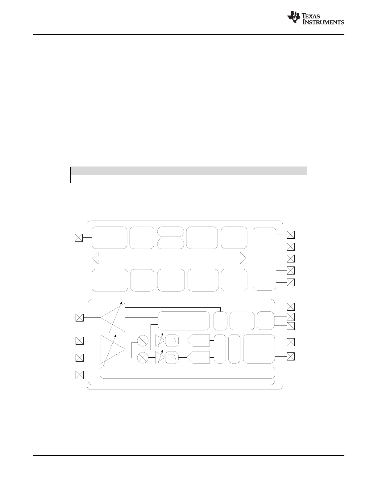
1.4 Functional Block Diagram
Figure 1-1 shows the system block diagram of the CC120x family of devices.
(1)
Device Information
Figure 1-1. System Block Diagram
2 Device Overview Copyright © 2013–2014, Texas Instruments Incorporated
Submit Documentation Feedback
Product Folder Links: CC1201

CC1201
www.ti.com
SWRS154B –OCTOBER 2013–REVISED OCTOBER 2014
Table of Contents
1 Device Overview ......................................... 1 4.15 40-MHz Clock Input (TCXO)........................ 16
1.1 Features .............................................. 1 4.16 32-kHz Clock Input.................................. 17
1.2 Applications........................................... 1 4.17 40-kHz RC Oscillator................................ 17
1.3 Description............................................ 2 4.18 I/O and Reset ....................................... 17
1.4 Functional Block Diagram ............................ 2 4.19 Temperature Sensor ................................ 17
2 Revision History ......................................... 4 4.20 Typical Characteristics.............................. 18
3 Terminal Configuration and Functions.............. 5 5 Detailed Description ................................... 21
3.1 Pin Diagram .......................................... 5 5.1 Block Diagram....................................... 21
3.2 Pin Configuration ..................................... 6 5.2 Frequency Synthesizer.............................. 21
4 Specifications ............................................ 7 5.3 Receiver............................................. 22
4.1 Absolute Maximum Ratings .......................... 7 5.4 Transmitter .......................................... 22
4.2 Handling Ratings ..................................... 7 5.5 Radio Control and User Interface................... 22
4.3 Recommended Operating Conditions (General
Characteristics) ....................................... 7
4.4 Thermal Resistance Characteristics for RHB
Package .............................................. 7
4.5 RF Characteristics.................................... 8
4.6 Regulatory Standards ................................ 8
4.7 Current Consumption, Static Modes ................. 9
4.8 Current Consumption, Transmit Modes .............. 9
4.9 Current Consumption, Receive Modes.............. 10
4.10 Receive Parameters................................. 11
4.11 Transmit Parameters................................ 14
4.12 PLL Parameters..................................... 15
4.13 Wake-up and Timing................................ 16
4.14 40-MHz Crystal Oscillator........................... 16
5.6 Enhanced Wake-On-Radio (eWOR)................ 22
5.7 RX Sniff Mode....................................... 23
5.8 Antenna Diversity ................................... 23
5.9 WaveMatch.......................................... 24
6 Typical Application Circuit........................... 25
7 Device and Documentation Support ............... 26
7.1 Device Support...................................... 26
7.2 Documentation Support............................. 27
7.3 Community Resources.............................. 27
7.4 Trademarks.......................................... 27
7.5 Electrostatic Discharge Caution..................... 27
7.6 Glossary............................................. 27
8 Mechanical Packaging and Orderable
Information .............................................. 28
Copyright © 2013–2014, Texas Instruments Incorporated Table of Contents 3
Submit Documentation Feedback
Product Folder Links: CC1201

CC1201
SWRS154B –OCTOBER 2013–REVISED OCTOBER 2014
www.ti.com
2 Revision History
NOTE: Page numbers for previous revisions may differ from page numbers in the current version.
This data manual revision history highlights the changes made to the SWRS154A device-specific data
manual to make it an SWRS154B revision.
Changes from Revision A (June 2014) to Revision B Page
• Added Ambient to the temperature range condition and removed Tj from Temperature range ........................... 7
• Added data to TCXO table......................................................................................................... 16
4 Revision History Copyright © 2013–2014, Texas Instruments Incorporated
Submit Documentation Feedback
Product Folder Links: CC1201
www.ti.com
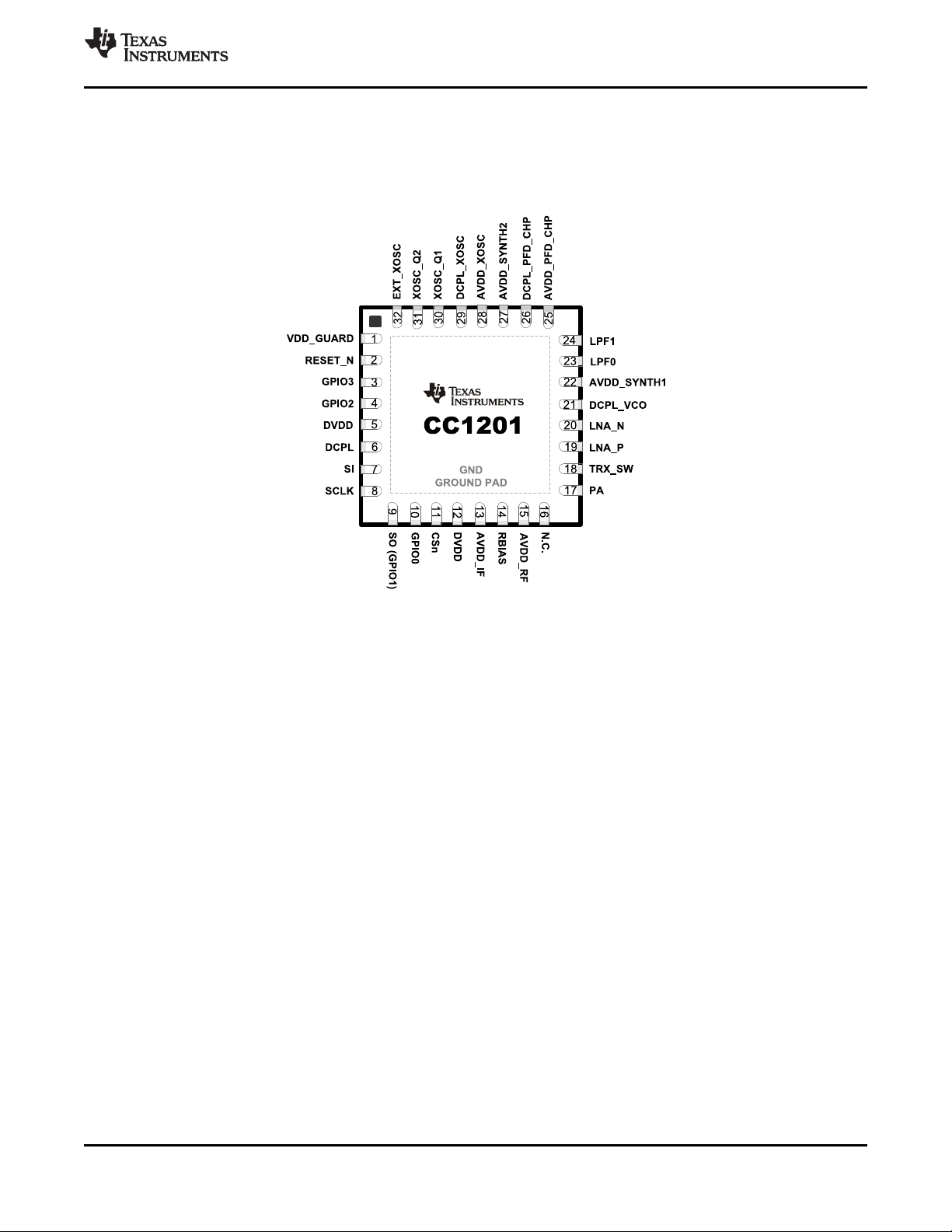
3 Terminal Configuration and Functions
3.1 Pin Diagram
Figure 3-1 shows pin names and locations for the CC1201 device.
CC1201
SWRS154B –OCTOBER 2013–REVISED OCTOBER 2014
Figure 3-1. Package 5-mm × 5-mm QFN
Copyright © 2013–2014, Texas Instruments Incorporated Terminal Configuration and Functions 5
Submit Documentation Feedback
Product Folder Links: CC1201
CC1201
SWRS154B –OCTOBER 2013–REVISED OCTOBER 2014
3.2 Pin Configuration
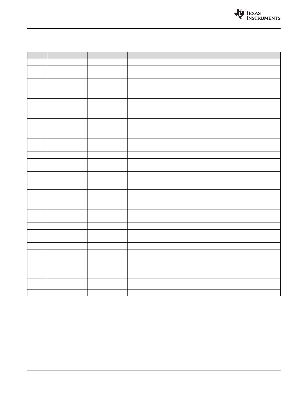
The following table lists the pin-out configuration for the CC1201 device.
PIN NO. PIN NAME TYPE / DIRECTION DESCRIPTION
1 VDD_GUARD Power 2.0–3.6 V VDD
2 RESET_N Digital input Asynchronous, active-low digital reset
3 GPIO3 Digital I/O General-purpose I/O
4 GPIO2 Digital I/O General-purpose I/O
5 DVDD Power 2.0–3.6 VDD to internal digital regulator
6 DCPL Power Digital regulator output to external decoupling capacitor
7 SI Digital input Serial data in
8 SCLK Digital input Serial data clock
9 SO(GPIO1) Digital I/O Serial data out (general-purpose I/O)
10 GPIO0 Digital I/O General-purpose I/O
11 CSn Digital input Active-low chip select
12 DVDD Power 2.0–3.6 V VDD
13 AVDD_IF Power 2.0–3.6 V VDD
14 RBIAS Analog External high-precision resistor
15 AVDD_RF Power 2.0–3.6 V VDD
16 N.C. Not connected
17 PA Analog Single-ended TX output (requires DC path to VDD)
18 TRX_SW Analog
19 LNA_P Analog Differential RX input (requires DC path to ground)
20 LNA_N Analog Differential RX input (requires DC path to ground)
21 DCPL_VCO Power Pin for external decoupling of VCO supply regulator
22 AVDD_SYNTH1 Power 2.0–3.6 V VDD
23 LPF0 Analog External loopfilter components
24 LPF1 Analog External loopfilter components
25 AVDD_PFD_CHP Power 2.0–3.6 V VDD
26 DCPL_PFD_CHP Power Pin for external decoupling of PFD and CHP regulator
27 AVDD_SYNTH2 Power 2.0–3.6 V VDD
28 AVDD_XOSC Power 2.0–3.6 V VDD
29 DCPL_XOSC Power Pin for external decoupling of XOSC supply regulator
30 XOSC_Q1 Analog
31 XOSC_Q2 Analog
32 EXT_XOSC Digital input
– GND Ground pad The ground pad must be connected to a solid ground plane.
TX and RX switch. Connected internally to GND in TX and floating (highimpedance) in RX.
Crystal oscillator pin 1 (must be grounded if a TCXO or other external clock
connected to EXT_XOSC is used)
Crystal oscillator pin 2 (must be left floating if a TCXO or other external clock
connected to EXT_XOSC is used)
Pin for external clock input (must be grounded if a regular crystal connected to
XOSC_Q1 and XOSC_Q2 is used)
www.ti.com
6 Terminal Configuration and Functions Copyright © 2013–2014, Texas Instruments Incorporated
Submit Documentation Feedback
Product Folder Links: CC1201
www.ti.com
4 Specifications
All measurements performed on CC1200EM_868_930 rev.1.0.0, CC1200EM_420_470 rev.1.0.1, or
CC1200EM_169 rev.1.2.
CC1201
SWRS154B –OCTOBER 2013–REVISED OCTOBER 2014
4.1 Absolute Maximum Ratings
(1)(2)
over operating free-air temperature range (unless otherwise noted)
PARAMETER MIN MAX UNIT CONDITION
Supply voltage (VDD, AVDD_x) –0.3 3.9 V All supply pins must have the same voltage
Input RF level +10 dBm
Voltage on any digital pin –0.3 VDD+0.3 V max 3.9 V
Voltage on any analog Pin
(including DCPL pins)
–0.3 2.0 V
(1) Stresses beyond those listed under absolute maximum ratings may cause permanent damage to the device. These are stress ratings
only, and functional operation of the device at these or any other conditions beyond those indicated under recommended operating
conditions is not implied. Exposure to absolute-maximum-rated conditions for extended periods may affect device reliability.
(2) All voltage values are with respect to VSS, unless otherwise noted.
4.2 Handling Ratings
MIN MAX UNIT
T
stg
V
ESD
Storage temperature range –40 125 °C
Electrostatic Human body model (HBM), per ANSI/ESDA/JEDEC JS001
discharge
(ESD)
performance:
Charged device model (CDM), per JESD22-
(2)
C101
All pins –500 500 V
(1)
–2 2 kV
(1) JEDEC document JEP155 states that 500-V HBM allows safe manufacturing with a standard ESD control process.
(2) JEDEC document JEP157 states that 250-V HBM allows safe manufacturing with a standard ESD control process.
4.3 Recommended Operating Conditions (General Characteristics)
PARAMETER MIN TYP MAX UNIT CONDITION
Voltage supply range 2.0 3.6 V All supply pins must have the same voltage
Voltage on digital inputs 0 VDD V
Temperature range –40 85 °C Ambient
4.4 Thermal Resistance Characteristics for RHB Package
(1)
Rθ
Rθ
Rθ
Psi
Psi
Rθ
°C/W
JC
JB
JA
JC
Junction-to-case (top) 21.1 0.00
Junction-to-board 5.3 0.00
Junction-to-free air 31.3 0.00
Junction-to-package top 0.2 0.00
JT
Junction-to-board 5.3 0.00
JB
Junction-to-case (bottom) 0.8 0.00
AIR FLOW (m/s)
(1) These values are based on a JEDEC-defined 2S2P system (with the exception of the Theta JC [RΘJC] value, which is based on a
JEDEC-defined 1S0P system) and will change based on environment as well as application. For more information, see these
EIA/JEDEC standards:
• JESD51-2, Integrated Circuits Thermal Test Method Environmental Conditions - Natural Convection (Still Air)
• JESD51-3, Low Effective Thermal Conductivity Test Board for Leaded Surface Mount Packages
• JESD51-7, High Effective Thermal Conductivity Test Board for Leaded Surface Mount Packages
• JESD51-9, Test Boards for Area Array Surface Mount Package Thermal Measurements
Power dissipation of 40 mW and an ambient temperature of 25ºC is assumed.
(2) m/s = meters per second
Copyright © 2013–2014, Texas Instruments Incorporated Specifications 7
Submit Documentation Feedback
Product Folder Links: CC1201
(2)
CC1201
SWRS154B –OCTOBER 2013–REVISED OCTOBER 2014
4.5 RF Characteristics
PARAMETER MIN TYP MAX UNIT CONDITION
820 950 MHz
410 475 MHz
Frequency bands
Frequency resolution 15 Hz In 410–475 MHz band
Data rate
164 190 MHz
(274) (316.6) MHz
(205) (237.5) MHz
(137) (158.3) MHz
30 Hz In 820–950 MHz band
6 Hz In 164–190 MHz band
0 1250 kbps Packet mode
0 625 kbps Transparent mode
Contact TI for more information about the use
of these frequency bands.
4.6 Regulatory Standards
PERFORMANCE MODE
High-performance mode ETSI EN 300 220 receiver categories
Low-power mode
FREQUENCY BAND SUITABLE FOR COMPLIANCE COMMENTS
820–950 MHz 2 and 3
410–475 MHz allowed output power in the
164–190 MHz ETSI EN 300 220 allowed output power in the
820–950 MHz
410–475 MHz
164–190 MHz ETSI EN 300 220
ETSI EN 300 220 receiver categories
ETSI EN 300 220 receiver categories
ETSI EN 300 220 receiver categories
WITH
ARIB STD-T108
FCC PART 15.247
FCC PART 15.249
2 and 3
2 and 3
FCC PART 15.247
FCC PART 15.249
2 and 3
Performance also suitable for
systems targeting maximum
allowed output power in the
respective bands, using a
range extender such as the
CC1190
Performance also suitable for
systems targeting maximum
respective bands, using a
range extender
Performance also suitable for
systems targeting maximum
respective bands, using a
range extender
www.ti.com
8 Specifications Copyright © 2013–2014, Texas Instruments Incorporated
Submit Documentation Feedback
Product Folder Links: CC1201
CC1201
www.ti.com
SWRS154B –OCTOBER 2013–REVISED OCTOBER 2014
4.7 Current Consumption, Static Modes
TA= 25°C, VDD = 3.0 V (unless otherwise noted)
PARAMETER MIN TYP MAX UNIT CONDITION
Power down with retention
XOFF mode 180 µA Crystal oscillator / TCXO disabled
IDLE mode 1.5 mA Clock running, system waiting with no radio activity
0.12 1 µA
0.5 µA Low-power RC oscillator running
4.8 Current Consumption, Transmit Modes
4.8.1 868-, 915-, and 920-MHz Bands (High-Performance Mode)
TA= 25°C, VDD = 3.0 V (unless otherwise noted)
PARAMETER MIN TYP MAX UNIT CONDITION
TX current consumption +14 dBm 46 mA
TX current consumption +10 dBm 36 mA
4.8.2 433-MHz Band (High-Performance Mode)
TA= 25°C, VDD = 3.0 V (unless otherwise noted)
PARAMETER MIN TYP MAX UNIT CONDITION
TX current consumption +15 dBm 49 mA
TX current consumption +14 dBm 46 mA
TX current consumption +10 dBm 35 mA
Copyright © 2013–2014, Texas Instruments Incorporated Specifications 9
Submit Documentation Feedback
Product Folder Links: CC1201

CC1201
SWRS154B –OCTOBER 2013–REVISED OCTOBER 2014
www.ti.com
4.8.3 169-MHz Band (High Performance Mode)
TA= 25°C, VDD = 3.0 V (unless otherwise noted)
PARAMETER MIN TYP MAX UNIT CONDITION
TX current consumption +15 dBm 54 mA
TX current consumption +14 dBm 50 mA
TX current consumption +10 dBm 39 mA
4.8.4 Low-Power Mode
TA= 25°C, VDD = 3.0 V, fc= 869.5 MHz (unless otherwise noted)
PARAMETER MIN TYP MAX UNIT CONDITION
TX Current Consumption +10 dBm 33.6 mA
4.9 Current Consumption, Receive Modes
4.9.1 High-Performance Mode
TA= 25°C, VDD = 3.0 V, fc= 869.5 MHz (unless otherwise noted)
PARAMETER MIN TYP MAX UNIT CONDITION
RX wait for sync Using RX Sniff Mode, where the receiver wakes up
1.2 kbps, 4-byte preamble 0.5 mA
38.4 kbps, 12-byte preamble 3.5 mA
50 kbps, 24-byte preamble 2.1 mA
RX peak current
1.2 kbps 23.6 mA
Average current consumption
Check for data packet every 1 second using 8 µA
eWOR
(1) See the sniff mode design note for more information (SWRA428)
at regular intervals looking for an incoming packet.
Sniff mode configured to terminate on carrier
sense, and is measured using RSSI_VALID
_COUNT = 1 (0 for 1.2 kbps), AGC_WIN_SIZE = 0,
and SETTLE_WAIT = 1.
Peak current consumption during packet reception
50 kbps, 5-byte preamble, 40-kHz RC oscillator
used as eWOR timer
(1)
4.9.2 Low-Power Mode
TA= 25°C, VDD = 3.0 V, fc= 869.5 MHz (unless otherwise noted)
PARAMETER MIN TYP MAX UNIT CONDITION
RX Peak current low-power RX mode
50 kbps 19 mA
Peak current consumption during packet reception
at the sensitivity limit
10 Specifications Copyright © 2013–2014, Texas Instruments Incorporated
Submit Documentation Feedback
Product Folder Links: CC1201
CC1201
www.ti.com
SWRS154B –OCTOBER 2013–REVISED OCTOBER 2014
4.10 Receive Parameters
All RX measurements made at the antenna connector, to a bit error rate (BER) limit of 1%. Selectivity and
blocking is measured with the desired signal 3 dB above the sensitivity level.
4.10.1 General Receive Parameters (High-Performance Mode)
TA= 25°C, VDD = 3.0 V, fc= 869.5 MHz (unless otherwise noted)
PARAMETER MIN TYP MAX UNIT CONDITION
Saturation +10 dBm
Digital channel filter programmable
bandwidth
IIP3 –14 dBm At maximum gain
Data rate offset tolerance
Spurious emissions
1–13 GHz (VCO leakage at 3.5 GHz) < –56 dBm
30 MHz to 1 GHz < –57 dBm
Optimum source impedance
868-, 915-, and 920-MHz bands 60 + j60 / 30 + j30 Ω
433-MHz band 100 + j60 / 50 + j30 Ω
169-MHz band 140 + j40 / 70 + j20 Ω
50 1600 kHz
±14 % With carrier sense detection enabled
±1600 ppm With carrier sense detection disabled
Radiated emissions measured according to ETSI
EN 300 220, fc= 869.5 MHz
(Differential or Single-Ended RX Configurations)
Copyright © 2013–2014, Texas Instruments Incorporated Specifications 11
Submit Documentation Feedback
Product Folder Links: CC1201
CC1201
SWRS154B –OCTOBER 2013–REVISED OCTOBER 2014
4.10.2 RX Performance in 868-, 915-, and 920-MHz Bands (High-Performance Mode)
TA= 25°C, VDD = 3.0 V (unless otherwise noted)
PARAMETER MIN TYP MAX UNIT CONDITION
–119 dBm 1.2 kbps 2-FSK, DEV=20 kHz CHF=50 kHz
–113 dBm 4.8 kbps OOK CHF=128 kHz
32.768 kbps 2-GFSK, DEV=50 kHz CHF=208
(1)
kHz
Sensitivity
–108 dBm
–110 dBm 38.4 kbps 2-GFSK, DEV=20 kHz CHF=104 kHz
–109 dBm 50 kbps 2-GFSK, DEV=25 kHz, CHF=104 kHz
–97 dBm 500 kbps 2-GMSK, CHF=833 kHz
–97 dBm 1 Mbps 4-GFSK, DEV=400 kHz, CHF=1.66 MHz
Blocking and selectivity
1.2-kbps 2-FSK, 50-kHz channel
separation, 20-kHz deviation, 50-kHz
channel filter
Blocking and selectivity
32.768-kbps 2-GFSK, 200-kHz channel
separation, 50-kHz deviation, 208-kHz
channel filter
Blocking and selectivity
38.4-kbps 2-GFSK, 100-kHz channel
separation, 20-kHz deviation, 104-kHz
channel filter
Blocking and selectivity
50-kbps 2-GFSK, 200-kHz channel
separation, 25-kHz deviation, 104-kHz
channel filter (Same modulation format as
802.15.4g Mandatory Mode)
50 dB ± 50 kHz (adjacent channel)
50 dB ± 100 kHz (alternate channel)
75 dB ± 2 MHz
80 dB ± 10 MHz
38 dB ± 200 kHz
46 dB ± 400 kHz
66 dB ± 2 MHz
70 dB ± 10 MHz
44 dB + 100 kHz (adjacent channel)
44 dB ± 200 kHz (alternate channel)
64 dB ± 2 MHz
72 dB ± 10 MHz
41 dB ± 200 kHz (adjacent channel)
46 dB ± 400 kHz (alternate channel)
65 dB ± 2 MHz
71 dB ± 10 MHz
45 dB ± 400 kHz (adjacent channel)
Blocking and selectivity
100-kbps 2-GFSK, 50-kHz deviation,
208-kHz channel filter
54 dB ± 800 kHz (alternate channel)
63 dB ± 2 MHz
68 dB ± 10 MHz
42 dB + 1 MHz (adjacent channel)
Blocking and selectivity
500-kbps GMSK, 833-kHz channel filter
42 dB ± 2 MHz (alternate channel)
57 dB ± 10 MHz
Blocking and selectivity
46 dB ± 2 MHz (adjacent channel)
1-Mbps 4-GFSK, 400-kHz deviation, 52 dB ± 4 MHz (alternate channel)
1.6-MHz channel filter
59 dB ± 10 MHz
(1) DEV is short for deviation, CHF is short for Channel Filter Bandwidth
(1)
www.ti.com
(1)
(1)
(1)
(1)
(1)
12 Specifications Copyright © 2013–2014, Texas Instruments Incorporated
Submit Documentation Feedback
Product Folder Links: CC1201

CC1201
www.ti.com
SWRS154B –OCTOBER 2013–REVISED OCTOBER 2014
4.10.3 RX Performance in 433-MHz Band (High-Performance Mode)
TA= 25°C, VDD = 3.0 V (unless otherwise noted)
PARAMETER MIN TYP MAX UNIT CONDITION
Sensitivity
Blocking and selectivity
1.2-kbps 2-FSK, 50-kHz channel
separation, 20-kHz deviation, 50-kHz
channel filter
Blocking and selectivity
38.4-kbps 2-GFSK, 100-kHz channel
separation, 20-kHz deviation, 104-kHz
channel filter
(1) DEV is short for deviation, CHF is short for Channel Filter Bandwidth
–120 dBm
–111 dBm 38.4 kbps 2-GFSK, DEV=20 kHz CHF=104 kHz
56 dB ± 50 kHz (adjacent channel)
56 dB ± 100 kHz (alternate channel)
79 dB ± 2 MHz
84 dB ± 10 MHz
49 dB + 100 kHz (adjacent channel)
48 dB ± 200 kHz (alternate channel)
66 dB ± 2 MHz
74 dB ± 10 MHz
1.2 kbps 2-FSK, DEV=20 kHz
CHF=50 kHz
(1)
4.10.4 RX Performance in 169-MHz Band (High-Performance Mode)
TA= 25°C, VDD = 3.0 V (unless otherwise noted)
PARAMETER MIN TYP MAX UNIT CONDITION
Sensitivity –119 dBm 1.2 kbps 2-FSK, DEV=20 kHz CHF=50 kHz
Blocking and Selectivity
1.2 kbps 2-FSK, 50 kHz channel
separation, 20 kHz deviation, 50 kHz
channel filter
Image rejection 1.2 kbps, DEV=20 kHz, CHF=50 kHz, image at
(Image compensation enabled) –417 kHz
(1) DEV is short for deviation, CHF is short for Channel Filter Bandwidth
62 dB ± 50 kHz (adjacent channel)
62 dB ± 100 kHz (alternate channel)
81 dB ± 2 MHz
85 dB ± 10 MHz
67 dB
(1)
(1)
(1)
4.10.5 RX Performance in Low-Power Mode
TA= 25°C, VDD = 3.0 V, fc= 869.5 MHz (unless otherwise noted)
PARAMETER MIN TYP MAX UNIT CONDITION
Sensitivity –96 dBm 50 kbps 2-GFSK, DEV=25 kHz, CHF=119 kHz
Blocking and selectivity 41 dB + 200 kHz (adjacent channel)
50 kbps 2-GFSK, 200-kHz channel
separation, 25-kHz deviation, 104-kHz
channel filter
(Same modulation format as 802.15.4g
Mandatory Mode)
Saturation 10 dBm
(1) DEV is short for deviation, CHF is short for Channel Filter Bandwidth
45 dB + 400 kHz (alternate channel)
62 dB ± 2 MHz
60 dB ± 10 MHz
(1)
Copyright © 2013–2014, Texas Instruments Incorporated Specifications 13
Submit Documentation Feedback
Product Folder Links: CC1201

CC1201
SWRS154B –OCTOBER 2013–REVISED OCTOBER 2014
4.11 Transmit Parameters
TA= 25°C, VDD = 3.0 V, fc= 869.5 MHz (unless otherwise noted)
PARAMETER MIN TYP MAX UNIT CONDITION
+14 dBm At 915/920 MHz
+15 dBm At 915/920 MHz with VDD = 3.6 V
+15 dBm At 868 MHz
Max output power
Min output power
Output power step size 0.4 dB Within fine step size range
Adjacent channel power –60 dBc
Spurious emissions
(Excluding harmonics)
30 MHz–1 GHz < –57 dBm EN 300-220, FCC part 15, ARIB STD-T108
1–12.75 GHz < –50 dBm
Harmonics
Second Harm, 169 MHz (ETSI) –43 dBm
Third Harm, 169 MHz (ETSI) –57 dBm
Fourth Harm, 169 MHz (ETSI) –63 dBm
+16 dBm At 868 MHz with VDD = 3.6 V
+15 dBm At 433 MHz
+16 dBm At 433 MHz with VDD = 3.6 V
+15 dBm At 169 MHz
+16 dBm At 169 MHz with VDD = 3.6 V
–12 dBm Within fine step size range
–38 dBm Within coarse step size range
4-GFSK 9.6 kbps in 12.5 kHz channel, measured in
8.75 kHz bandwidth (ETSI 300 220 compliant)
Transmission at +14 dBm
Suitable for systems targeting compliance with ETSI
Measured in 1 MHz bandwidth
www.ti.com
Second Harm, 433 MHz (ETSI) –59 dBm
Third Harm, 433 MHz (ETSI) –51 dBm
Fourth Harm, 433 MHz (ETSI) –63 dBm
Second Harm, 868 MHz (ETSI) –50 dBm using TI reference design
Third Harm, 868 MHz (ETSI) –44 dBm
Fourth Harm, 868 MHz (ETSI) –56 dBm
Second Harm, 915 MHz (FCC) –58 dBm
Third Harm, 915 MHz (FCC) –46 dBm
Fourth Harm, 915 MHz (FCC) –62 dBm
Second Harm, 920 MHz (ARIB) –65 dBm
Third Harm, 920 MHz (ARIB) –60 dBm
Optimum load impedance
868-, 915-, and 920-MHz bands 35 + j35 Ω
433-MHz band 55 + j25 Ω
169-MHz band 80 + j0 Ω
Transmission at +14 dBm (or maximum allowed in
applicable band where this is less than +14 dBm)
Suitable for systems targeting compliance with ETSI
EN 300-220, FCC part 15, ARIB STD-T108
14 Specifications Copyright © 2013–2014, Texas Instruments Incorporated
Submit Documentation Feedback
Product Folder Links: CC1201

www.ti.com
SWRS154B –OCTOBER 2013–REVISED OCTOBER 2014
4.12 PLL Parameters
4.12.1 High Performance Mode
TA= 25°C, VDD = 3.0 V (unless otherwise noted)
PARAMETER MIN TYP MAX UNIT CONDITION
–94 dBc/Hz ± 10 kHz offset
Phase noise in 868-, 915-, and 920-MHz
Bands
200-kHz loop bandwidth setting
Phase noise in 868-, 915-, and 920-MHz
Bands
300-kHz loop bandwidth setting
Phase noise in 868-, 915-, and 920-MHz
Bands
400-kHz loop bandwidth setting
Phase noise in 868-, 915-, and 920-MHz
Bands
500-kHz loop bandwidth setting
Phase noise in 433-MHz band
300-kHz loop bandwidth setting
Phase noise in 169-MHz band
300-kHz loop bandwidth setting
–96 dBc/Hz ± 100 kHz offset
–123 dBc/Hz ± 1 MHz offset
–137 dBc/Hz ± 10 MHz offset
–100 dBc/Hz ± 10 kHz offset
–102 dBc/Hz ± 100 kHz offset
–121 dBc/Hz ± 1 MHz offset
–136 dBc/Hz ± 10 MHz offset
–103 dBc/Hz ± 10 kHz offset
–104 dBc/Hz ± 100 kHz offset
–119 dBc/Hz ± 1 MHz offset
–133 dBc/Hz ± 10 MHz offset
–104 dBc/Hz ± 10 kHz offset
–106 dBc/Hz ± 100 kHz offset
–116 dBc/Hz ± 1 MHz offset
–130 dBc/Hz ± 10 MHz offset
–106 dBc/Hz ± 10 kHz offset
–107 dBc/Hz ± 100 kHz offset
–127 dBc/Hz ± 1 MHz offset
–141 dBc/Hz ± 10 MHz offset
–114 dBc/Hz ± 10 kHz offset
–114 dBc/Hz ± 100 kHz offset
–132 dBc/Hz ± 1 MHz offset
–142 dBc/Hz ± 10 MHz offset
CC1201
4.12.2 Low-Power Mode
PARAMETER MIN TYP MAX UNIT CONDITION
–99 dBc/Hz ± 10 kHz offset
Phase noise in 868-, 915-, and 920-MHz
bands
200-kHz loop bandwidth setting
Copyright © 2013–2014, Texas Instruments Incorporated Specifications 15
–101 dBc/Hz ± 100 kHz offset
–121 dBc/Hz ± 1 MHz offset
–135 dBc/Hz ± 10 MHz offset
Submit Documentation Feedback
Product Folder Links: CC1201

CC1201
SWRS154B –OCTOBER 2013–REVISED OCTOBER 2014
www.ti.com
4.13 Wake-up and Timing
TA= 25°C, VDD = 3.0 V, fc= 869.5 MHz (unless otherwise noted)
The turnaround behavior to and from RX and/or TX is highly configurable, and the time it takes will depend on
how the device is set up. See the CC120X user guide (SWRU346) for more information.
PARAMETER MIN TYP MAX UNIT CONDITION
Powerdown to IDLE 0.24 ms Depends on crystal
IDLE to RX/TX
RX/TX turnaround 43 µs
RX-to-RX turnaround
TX-to-TX turnaround
RX/TX to IDLE time
Frequency synthesizer calibration 314 µs When using SCAL strobe
Minimum required number of preamble Required for RF front end gain settling only. Digital
bytes demodulation does not require preamble for settling
Time from start RX until valid RSSI
Including gain settling (function of channel
bandwidth. Programmable for trade-off
between speed and accuracy)
(1) See the design note on RSSI and response time. It is written for the CC112X devices, but the same principles apply for the CC1201
device.
(1)
133 µs Calibration disabled
369 µs Calibration enabled
369 µs With PLL calibration
0 µs Without PLL calibration
369 µs With PLL calibration
0 µs Without PLL calibration
237 µs Calibrate when leaving RX/TX enabled
0 µs Calibrate when leaving RX/TX disabled
0.5 bytes
0.25 ms 120-kHz channels
4.14 40-MHz Crystal Oscillator
TA= 25°C, VDD = 3.0 V (unless otherwise noted)
PARAMETER MIN TYP MAX UNIT CONDITION
It is expected that there will be degraded sensitivity
at multiples of XOSC/2 in RX, and an increase in
spurious emissions when the RF channel is close to
Crystal frequency 38.4 40 MHz
Load capacitance (CL) 10 pF
ESR 60 Ω Simulated over operating conditions
Start-up time 0.24 ms Depends on crystal
multiples of XOSC in TX. We recommend that the
RF channel is kept RX_BW/2 away from XOSC/2 in
RX, and that the level of spurious emissions be
evaluated if the RF channel is closer than 1 MHz to
multiples of XOSC in TX.
4.15 40-MHz Clock Input (TCXO)
TA= 25°C, VDD = 3.0 V if nothing else stated
PARAMETER MIN TYP MAX UNIT CONDITION
Clock frequency 38.4 40 MHz
TCXO with CMOS output TCXO with CMOS output directly
High input voltage 1.4 VDD V
Low input voltage 0 0.6 V
Rise / Fall time 2 ns
Clipped sine output TCXO clipped sine output connected
Clock input amplitude (peak-to-peak)
0.8 1.5 V
coupled to pin EXT_OSC
to pin EXT_OSC through series
capacitor
16 Specifications Copyright © 2013–2014, Texas Instruments Incorporated
Submit Documentation Feedback
Product Folder Links: CC1201

www.ti.com
SWRS154B –OCTOBER 2013–REVISED OCTOBER 2014
4.16 32-kHz Clock Input
TA= 25°C, VDD = 3.0 V (unless otherwise noted)
PARAMETER MIN TYP MAX UNIT CONDITION
Clock frequency 32 kHz
32-kHz clock input pin input high voltage 0.8 x VDD V
32-kHz clock input pin input low voltage 0.2 x VDD V
4.17 40-kHz RC Oscillator
TA= 25°C, VDD = 3.0 V (unless otherwise noted)
PARAMETER MIN TYP MAX UNIT CONDITION
Frequency 40 kHz
Frequency accuracy after calibration ±0.1 %
Initial calibration time 1.32 ms
After calibration (frequency calibrated against the
40-MHz crystal or TCXO)
Relative to frequency reference (that is, 40-MHz
crystal or TCXO)
4.18 I/O and Reset
TA= 25°C, VDD = 3.0 V (unless otherwise noted)
PARAMETER MIN TYP MAX UNIT CONDITION
Logic input high voltage V
Logic input low voltage V
Logic output high voltage V
Logic output low voltage V
Power-on reset threshold 1.3 V Voltage on DVDD pin
0.8 x
VDD
0.8 x
VDD
0.2 x
VDD
0.2 x
VDD
At 4-mA output load or less
CC1201
4.19 Temperature Sensor
TA= 25°C, VDD = 3.0 V (unless otherwise noted).
PARAMETER MIN TYP MAX UNIT CONDITION
Temperature sensor range –40 85 °C
Temperature coefficient 2.66 mV / °C
Typical output voltage 794 mV
VDD coefficient 1.17 mV / V
The CC1201 device can be configured to provide a voltage proportional to temperature on GPIO1. The
temperature can be estimated by measuring this voltage (see Section 4.19, Temperature Sensor). For more
information, see the temperature sensor design note (SWRA415).
Change in sensor output voltage versus change in
temperature
Typical sensor output voltage at TA = 25°C, VDD =
3.0 V
Change in sensor output voltage versus change in
VDD
Copyright © 2013–2014, Texas Instruments Incorporated Specifications 17
Submit Documentation Feedback
Product Folder Links: CC1201

0
10
20
30
40
50
60
TX Current (mA)
PApower setting
-50
-40
-30
-20
-10
0
10
20
Output Power (dBm)
PApower setting
10
11
12
13
14
15
16
2 2.5 3 3.5
Output Power (dBm)
Supply Voltage (V)
12
13
14
15
16
-40 0 40 80
Output Power (dBm)
Temperature (ºC)
-20
-10
0
10
20
30
40
50
60
70
80
-2 -1 0 1 2
Selectivity (dB)
Offset Frequency (MHz)
-40
-20
0
20
40
60
80
-110 -90 -70 -50 -30 -10
RSSI
Input Level (dBm)
CC1201
SWRS154B –OCTOBER 2013–REVISED OCTOBER 2014
4.20 Typical Characteristics
TA = 25°C, VDD = 3.0 V, fc= 869.5 MHz (unless otherwise noted)
www.ti.com
50-kbps GFSK, 25-kHz Deviation, 104-kHz Channel Filter Bandwidth
Figure 4-1. RSSI vs Input Level
Maximum Output Power Setting (0x7F)
Figure 4-3. Output Power vs Supply Voltage
50 kbps, 25-kHz Deviation, 104-kHz Channel Filter Bandwidth Image
Figure 4-2. Selectivity vs Offset Frequency (100-kHz Channels)
Frequency at –0.28-MHz Offset
Maximum Output Power Setting (0x7F)
Figure 4-4. Output Power vs Temperature
Figure 4-5. Output Power at 868 MHz
18 Specifications Copyright © 2013–2014, Texas Instruments Incorporated
vs PA Power Setting
Submit Documentation Feedback
Product Folder Links: CC1201
Figure 4-6. TX Current at 868 MHz
vs PA Power Setting

0
0.2
0.4
0.6
0.8
1
1.2
1.4
1.5
1.7
1.9
2.1
2.3
2.5
2.7
2.9
3.1
0 5 10 15 20 25 30
GPIO Output Low Voltage (V)
GPIO Output high Voltage (V)
Current (mA)
Output High Voltage
Output Low Voltage
www.ti.com
Typical Characteristics (continued)
CC1201
SWRS154B –OCTOBER 2013–REVISED OCTOBER 2014
1 Mbps 4-GFSK, 400-kHz Deviation 500-kHz Loop Bandwidth 1 Mbps 4-GFSK, 400-kHz Deviation 300-kHz Loop Bandwidth
1 kbps GFSK, 25-kHz Deviation 200-kHz Loop Bandwidth
Figure 4-7. Eye Diagram Figure 4-8. Eye Diagram
Figure 4-9. Eye Diagram
Figure 4-10. GPIO Output High and Low Voltage
vs Current Being Sourced and Sinked
Figure 4-11. Phase Noise 869.5 MHz (10-kHz to 100-MHz Offset) Figure 4-12. Phase Noise 869.5 MHz (10-kHz to 100-MHz Offset)
Copyright © 2013–2014, Texas Instruments Incorporated Specifications 19
200-kHz Loop Bandwidth 300-kHz Loop Bandwidth
Submit Documentation Feedback
Product Folder Links: CC1201

CC1201
SWRS154B –OCTOBER 2013–REVISED OCTOBER 2014
Typical Characteristics (continued)
www.ti.com
Figure 4-13. Phase Noise 869.5 MHz (10-kHz to 100-MHz Offset)
400-kHz Loop Bandwidth
Figure 4-14. Phase Noise 869.5 MHz (10-kHz to 100-MHz Offset)
500-kHz Loop Bandwidth
20 Specifications Copyright © 2013–2014, Texas Instruments Incorporated
Submit Documentation Feedback
Product Folder Links: CC1201

BIAS
RBIAS
XOSC_Q1
XOSC_Q2
XOSC
LNA
0
90
FREQ
SYNTH
ADC
ADC
DEMODULATOR
PACKET HANDLER
RXFIFO
MODULATOR
TXFIFO
RADIO CONTROL & POWER MANAGEMENT
LNA_P
LNA_N
PA
EXT_XOSC
PA
LFC1
CS_N
SI
SO (GPIO0)
SCLK
GPIO2
GPIO1
GPIO3
DIGITAL INTERFACE TO MCU
LFC0
CC120x
MARC
Main Radio Control unit
Ultra low power 16 bit
MCU
256 byte
FIFO RAM
buffer
4 kbyte
ROM
RF and DSP frontend
Packet handler
and FIFO control
Configuration and
status registers
eWOR
Enhanced ultra low power
Wake On Radio timer
SPI
Serial configuration
and data interface
Interrupt and
IO handler
System bus
PA out
LNA_P
LNA_N
90 dB dynamic
range ADC
90 dB dynamic
range ADC
High linearity
LNA
+16 dBm high
efficiency PA
Channel
filter
XOSC
Cordic
AGC
Automatic Gain Control, 60dB VGA range
RSSI measurements and carrier sense detection
Highly flexible FSK / OOK
demodulator
(optional bit clock)
(optional low jitter serial
data output for legacy
protocols)
Data interface with
signal chain access
XOSC_Q1
XOSC_Q2
Ultra low power 40 kHz
auto-calibrated RC oscillator
(optional 40 kHz
clock input)
CSn (chip select)
SI (serial input)
SO (serial output)
SCLK (serial clock)
(optional GPIO3/2/0)
Modulator
Fully integrated fractional-N
frequency synthesizer
Output power ramping and OOK / ASK modulation
IF amp
IF amp
(optional auto detected
external XOSC / TCXO)
(optional GPIO for
antenna diversity)
I
Q
Battery sensor /
temp sensor
Power on reset
AES-128
accelerator
www.ti.com
5 Detailed Description
5.1 Block Diagram
Figure 5-1 shows the system block diagram of the CC120x family of devices.
CC1201
SWRS154B –OCTOBER 2013–REVISED OCTOBER 2014
Figure 5-1. System Block Diagram
5.2 Frequency Synthesizer
At the center of the CC1201 device there is a fully integrated, fractional-N, ultra-high-performance
frequency synthesizer. The frequency synthesizer is designed for excellent phase noise performance,
providing very high selectivity and blocking performance. The system is designed to comply with the most
stringent regulatory spectral masks at maximum transmit power.
Either a crystal can be connected to XOSC_Q1 and XOSC_Q2, or a TCXO can be connected to the
EXT_XOSC input. The oscillator generates the reference frequency for the synthesizer, as well as clocks
for the analog-to-digital converter (ADC) and the digital part. To reduce system cost, the CC1201 device
has high-accuracy frequency estimation and compensation registers to measure and compensate for
crystal inaccuracies. This compensation enables the use of lower cost crystals. If a TCXO is used, the
CC1201 device automatically turns on and off the TCXO when needed to support low-power modes and
Copyright © 2013–2014, Texas Instruments Incorporated Detailed Description 21
Wake-On-Radio operation.
Submit Documentation Feedback
Product Folder Links: CC1201

CC1201
SWRS154B –OCTOBER 2013–REVISED OCTOBER 2014
5.3 Receiver
The CC1201 device features a highly flexible receiver. The received RF signal is amplified by the lownoise amplifier (LNA) and is down-converted in quadrature (I/Q) to the intermediate frequency (IF). At IF,
the I/Q signals are digitized by the high dynamic-range ADCs.
An advanced automatic gain control (AGC) unit adjusts the front-end gain, and enables the CC1201
device to receive strong and weak signals, even in the presence of strong interferers. High-attenuation
channel and data filtering enable reception with strong neighbor channel interferers. The I/Q signal is
converted to a phase and magnitude signal to support the FSK and OOK modulation schemes.
A unique I/Q compensation algorithm removes any problem of I/Q mismatch, thus avoiding
time-consuming and costly I/Q image calibration steps.
5.4 Transmitter
The CC1201 transmitter is based on direct synthesis of the RF frequency (in-loop modulation). To use the
spectrum effectively, the CC1201 device has extensive data filtering and shaping in TX mode to support
high throughput data communication in narrowband channels. The modulator also controls power ramping
to remove issues such as spectral splattering when driving external high-power RF amplifiers.
www.ti.com
NOTE
5.5 Radio Control and User Interface
The CC1201 digital control system is built around the main radio control (MARC), which is implemented
using an internal high-performance, 16-bit ultra-low-power processor. MARC handles power modes, radio
sequencing, and protocol timing.
A 4-wire SPI serial interface is used for configuration, strobe commands, and FIFO access. The digital
baseband includes support for channel configuration, packet handling, and data buffering. The host MCU
can stay in sleep mode until a valid RF packet is received. This greatly reduces power consumption.
When the host MCU receives a valid RF packet, it burst-reads the data. This reduces the required
computing power.
The CC1201 radio control and user interface are based on the widely used CC1101 transceiver. This
relationship enables an easy transition between the two platforms. The command strobes and the main
radio states are the same for the two platforms.
For legacy formats, the CC1201 device also supports two serial modes.
• Synchronous serial mode: The CC1201 device performs bit synchronization and provides the MCU
with a bit clock with associated data.
• Transparent mode: The CC1201 device outputs the digital baseband signal using a digital interpolation
filter to eliminate jitter introduced by digital filtering and demodulation.
5.6 Enhanced Wake-On-Radio (eWOR)
eWOR, using a flexible integrated sleep timer, enables automatic receiver polling with no intervention from
the MCU. When the CC1201 device enters RX mode, it listens and then returns to sleep if a valid RF
packet is not received. The sleep interval and duty cycle can be configured to make a trade-off between
network latency and power consumption. Incoming messages are time-stamped to simplify timer resynchronization.
The eWOR timer runs off an ultra-low-power RC oscillator. To improve timing accuracy, the RC oscillator
can be automatically calibrated to the RF crystal in configurable intervals.
22 Detailed Description Copyright © 2013–2014, Texas Instruments Incorporated
Submit Documentation Feedback
Product Folder Links: CC1201

www.ti.com
5.7 RX Sniff Mode
The CC1201 device supports quick start up times, and requires few preamble bits. RX Sniff Mode uses
these conditions to dramatically reduce the current consumption while the receiver is waiting for data.
Because the CC1201 device can wake up and settle much faster than the duration of most preambles, it
is not required to be in RX mode continuously while waiting for a packet to arrive. Instead, the Enhanced
Wake On Radio feature can be used to put the device into sleep mode periodically. By setting an
appropriate sleep time, the CC1201 device can wake up and receive the packet when it arrives with no
performance loss. This sequence removes the need for accurate timing synchronization between
transmitter and receiver, and lets the user trade off current consumption between the transmitter and
receiver.
For more information, see the sniff mode design note (SWRA428).
5.8 Antenna Diversity
Antenna diversity can increase performance in a multipath environment. An external antenna switch is
required. The CC1201 device uses one of the GPIO pins to automatically control the switch. This device
also supports differential output control signals typically used in RF switches.
If antenna diversity is enabled, the GPIO alternates between high and low states until a valid RF input
signal is detected. An optional acknowledge packet can be transmitted without changing the state of the
GPIO.
CC1201
SWRS154B –OCTOBER 2013–REVISED OCTOBER 2014
An incoming RF signal can be validated by received signal strength or by using the automatic preamble
detector. Using the automatic preamble detector ensures a more robust system and avoids the need to
set a defined signal strength threshold (such a threshold sets the sensitivity limit of the system).
Copyright © 2013–2014, Texas Instruments Incorporated Detailed Description 23
Submit Documentation Feedback
Product Folder Links: CC1201

CC1201
SWRS154B –OCTOBER 2013–REVISED OCTOBER 2014
5.9 WaveMatch
Advanced capture logic locks onto the synchronization word and does not require preamble settling bytes.
Therefore, receiver settling time is reduced to the settling time of the AGC, typically 4 bits.
The WaveMatch feature also greatly reduces false sync triggering on noise, further reducing the power
consumption and improving sensitivity and reliability. The same logic can also be used as a highperformance preamble detector to reliably detect a valid preamble in the channel.
www.ti.com
See swrc046 for more information.
Figure 5-2. Receiver Configurator in SmartRF™ Studio
24 Detailed Description Copyright © 2013–2014, Texas Instruments Incorporated
Submit Documentation Feedback
Product Folder Links: CC1201

VDD
VDD
VDD
VDD
VDD
CC1201
5
4
3
2
1
6
7
8
13
12
11
10
9
14
15
16
20
21
22
23
24
19
18
17
28
29
30
31
32
27
26
25
VDD
VDD
40 MHz
crystal
Optional
XOSC/
TCXO
MCU connection
SPI interface and
optional gpio pins
VDD
VDD
VDD
(optional control pin
from CC1200)
AVDD_PFD_CHP
XOSC_Q2
XOSC_Q1
DCPL_PFD_CHP
AVDD_SYNTH2
DCPL_XOSC
AVDD_XOSC
EXT_XOSC
RESET_N
GPIO3
GPIO2
DVDD
VDD_GUARD
DCPL
SI
SCLK
CSn
SO (GPIO1)
DVDD
RBIAS
AVDD_IF
AVDD_RF
N.C.
GPIO0
LNA_P
LNA_N
DCPL_VCO
AVDD_SYNTH1
PA
TRX_SW
LPF0
LPF1
www.ti.com
6 Typical Application Circuit
This section is intended only as an introduction.
Very few external components are required for the operation of the CC1201 device. Figure 6-1 shows a
typical application circuit. The board layout will greatly influence the performance of the CC1201 device.
Figure 6-1 does not show decoupling capacitors for power pins.
CC1201
SWRS154B –OCTOBER 2013–REVISED OCTOBER 2014
NOTE
Copyright © 2013–2014, Texas Instruments Incorporated Typical Application Circuit 25
For more information, see the reference designs available for the CC1201 device in Section 7.2,
Documentation Support.
Figure 6-1. Typical Application Circuit
Submit Documentation Feedback
Product Folder Links: CC1201

CC1201
SWRS154B –OCTOBER 2013–REVISED OCTOBER 2014
7 Device and Documentation Support
7.1 Device Support
7.1.1 Development Support
7.1.1.1 Configuration Software
The CC1201 device can be configured using the SmartRF Studio software (SWRC046). The SmartRF
Studio software is highly recommended for obtaining optimum register settings, and for evaluating
performance and functionality.
7.1.2 Device and Development-Support Tool Nomenclature
To designate the stages in the product development cycle, TI assigns prefixes to the part numbers of all
microprocessors (MPUs) and support tools. Each device has one of three prefixes: X, P, or null (no prefix)
(for example, CC1201). Texas Instruments recommends two of three possible prefix designators for its
support tools: TMDX and TMDS. These prefixes represent evolutionary stages of product development
from engineering prototypes (TMDX) through fully qualified production devices and tools (TMDS).
Device development evolutionary flow:
X Experimental device that is not necessarily representative of the final device's electrical
specifications and may not use production assembly flow.
www.ti.com
P Prototype device that is not necessarily the final silicon die and may not necessarily meet
final electrical specifications.
null Production version of the silicon die that is fully qualified.
Support tool development evolutionary flow:
TMDX Development-support product that has not yet completed Texas Instruments internal
qualification testing.
TMDS Fully qualified development-support product.
X and P devices and TMDX development-support tools are shipped against the following disclaimer:
"Developmental product is intended for internal evaluation purposes."
Production devices and TMDS development-support tools have been characterized fully, and the quality
and reliability of the device have been demonstrated fully. TI's standard warranty applies.
Predictions show that prototype devices (X or P) have a greater failure rate than the standard production
devices. Texas Instruments recommends that these devices not be used in any production system
because their expected end-use failure rate still is undefined. Only qualified production devices are to be
used.
TI device nomenclature also includes a suffix with the device family name. This suffix indicates the
package type (for example, RHB), the temperature range (for example, blank is the default commercial
temperature range), and the device speed range, in megahertz. provides a legend for reading the
complete device name for any CC1201 device.
For orderable part numbers of CC1201 devices in the QFN package types, see the Package Option
Addendum of this document, the TI website (www.ti.com), or contact your TI sales representative.
26 Device and Documentation Support Copyright © 2013–2014, Texas Instruments Incorporated
Submit Documentation Feedback
Product Folder Links: CC1201

www.ti.com
7.2 Documentation Support
The following documents describe the CC1201 processor. Copies of these documents are available on the
Internet at www.ti.com. Tip: Enter the literature number in the search box provided at www.ti.com.
SWRR106 CC112x IPC 868- and 915-MHz 2-layer Reference Design
SWRR107 CC112x IPC 868- and 915-MHz 4-layer Reference Design
SWRR122 CC1201EM 420- to 470-MHz Reference Design
SWRR121 CC1201EM 868- to 930-MHz Reference Design
SWRC046 SmartRF Studio Software
SWRA428 CC112x/CC120x Sniff Mode Application Note
7.3 Community Resources
The following links connect to TI community resources. Linked contents are provided "AS IS" by the
respective contributors. They do not constitute TI specifications and do not necessarily reflect TI's views;
see TI's Terms of Use.
TI E2E™ Online Community TI's Engineer-to-Engineer (E2E) Community. Created to foster
collaboration among engineers. At e2e.ti.com, you can ask questions, share knowledge,
explore ideas and help solve problems with fellow engineers.
CC1201
SWRS154B –OCTOBER 2013–REVISED OCTOBER 2014
TI Embedded Processors Wiki Texas Instruments Embedded Processors Wiki. Established to help
developers get started with Embedded Processors from Texas Instruments and to foster
innovation and growth of general knowledge about the hardware and software surrounding
these devices.
7.4 Trademarks
SmartRF, E2E are trademarks of Texas Instruments.
All other trademarks are the property of their respective owners.
7.5 Electrostatic Discharge Caution
This integrated circuit can be damaged by ESD. Texas Instruments recommends that all integrated circuits be handled with
appropriate precautions. Failure to observe proper handling and installation procedures can cause damage.
ESD damage can range from subtle performance degradation to complete device failure. Precision integrated circuits may be more
susceptible to damage because very small parametric changes could cause the device not to meet its published specifications.
7.6 Glossary
SLYZ022 — TI Glossary.
This glossary lists and explains terms, acronyms, and definitions.
Copyright © 2013–2014, Texas Instruments Incorporated Device and Documentation Support 27
Submit Documentation Feedback
Product Folder Links: CC1201

CC1201
SWRS154B –OCTOBER 2013–REVISED OCTOBER 2014
8 Mechanical Packaging and Orderable Information
The following pages include mechanical packaging and orderable information. This information is the most
current data available for the designated devices. This data is subject to change without notice and
revision of this document. For browser-based versions of this data sheet, refer to the left-hand navigation.
www.ti.com
28 Mechanical Packaging and Orderable Information Copyright © 2013–2014, Texas Instruments Incorporated
Submit Documentation Feedback
Product Folder Links: CC1201

PACKAGE OPTION ADDENDUM
www.ti.com
11-Dec-2020
PACKAGING INFORMATION
Orderable Device Status
CC1201RHBR ACTIVE VQFN RHB 32 3000 RoHS & Green NIPDAU | NIPDAUAG Level-3-260C-168 HR -40 to 85 CC1201
CC1201RHBT ACTIVE VQFN RHB 32 250 RoHS & Green NIPDAU | NIPDAUAG Level-3-260C-168 HR -40 to 85 CC1201
(1)
The marketing status values are defined as follows:
ACTIVE: Product device recommended for new designs.
LIFEBUY: TI has announced that the device will be discontinued, and a lifetime-buy period is in effect.
NRND: Not recommended for new designs. Device is in production to support existing customers, but TI does not recommend using this part in a new design.
PREVIEW: Device has been announced but is not in production. Samples may or may not be available.
OBSOLETE: TI has discontinued the production of the device.
Package Type Package
(1)
Drawing
Pins Package
Qty
Eco Plan
(2)
Lead finish/
Ball material
(6)
MSL Peak Temp
(3)
Op Temp (°C) Device Marking
(4/5)
(2)
RoHS: TI defines "RoHS" to mean semiconductor products that are compliant with the current EU RoHS requirements for all 10 RoHS substances, including the requirement that RoHS substance
do not exceed 0.1% by weight in homogeneous materials. Where designed to be soldered at high temperatures, "RoHS" products are suitable for use in specified lead-free processes. TI may
reference these types of products as "Pb-Free".
RoHS Exempt: TI defines "RoHS Exempt" to mean products that contain lead but are compliant with EU RoHS pursuant to a specific EU RoHS exemption.
Green: TI defines "Green" to mean the content of Chlorine (Cl) and Bromine (Br) based flame retardants meet JS709B low halogen requirements of <=1000ppm threshold. Antimony trioxide based
flame retardants must also meet the <=1000ppm threshold requirement.
(3)
MSL, Peak Temp. - The Moisture Sensitivity Level rating according to the JEDEC industry standard classifications, and peak solder temperature.
(4)
There may be additional marking, which relates to the logo, the lot trace code information, or the environmental category on the device.
(5)
Multiple Device Markings will be inside parentheses. Only one Device Marking contained in parentheses and separated by a "~" will appear on a device. If a line is indented then it is a continuation
of the previous line and the two combined represent the entire Device Marking for that device.
(6)
Lead finish/Ball material - Orderable Devices may have multiple material finish options. Finish options are separated by a vertical ruled line. Lead finish/Ball material values may wrap to two
lines if the finish value exceeds the maximum column width.
Important Information and Disclaimer:The information provided on this page represents TI's knowledge and belief as of the date that it is provided. TI bases its knowledge and belief on information
provided by third parties, and makes no representation or warranty as to the accuracy of such information. Efforts are underway to better integrate information from third parties. TI has taken and
continues to take reasonable steps to provide representative and accurate information but may not have conducted destructive testing or chemical analysis on incoming materials and chemicals.
TI and TI suppliers consider certain information to be proprietary, and thus CAS numbers and other limited information may not be available for release.
In no event shall TI's liability arising out of such information exceed the total purchase price of the TI part(s) at issue in this document sold by TI to Customer on an annual basis.
Samples
Addendum-Page 1

PACKAGE OPTION ADDENDUM
www.ti.com
11-Dec-2020
Addendum-Page 2

PACKAGE MATERIALS INFORMATION
www.ti.com 12-Feb-2019
TAPE AND REEL INFORMATION
*All dimensions are nominal
Device Package
Type
CC1201RHBR VQFN RHB 32 3000 330.0 12.4 5.3 5.3 1.5 8.0 12.0 Q2
CC1201RHBT VQFN RHB 32 250 180.0 12.4 5.3 5.3 1.5 8.0 12.0 Q2
Package
Drawing
Pins SPQ Reel
Diameter
(mm)
Reel
Width
W1 (mm)
A0
(mm)B0(mm)K0(mm)P1(mm)W(mm)
Pin1
Quadrant
Pack Materials-Page 1

PACKAGE MATERIALS INFORMATION
www.ti.com 12-Feb-2019
*All dimensions are nominal
Device Package Type Package Drawing Pins SPQ Length (mm) Width (mm) Height (mm)
CC1201RHBR VQFN RHB 32 3000 350.0 350.0 43.0
CC1201RHBT VQFN RHB 32 250 210.0 185.0 35.0
Pack Materials-Page 2

GENERIC PACKAGE VIEW
VQFN - 1 mm max heightRHB 32
5 x 5, 0.5 mm pitch
PLASTIC QUAD FLATPACK - NO LEAD
Images above are just a representation of the package family, actual package may vary.
Refer to the product data sheet for package details.
www.ti.com
4224745/A

PACKAGE OUTLINE
PIN 1 INDEX AREA
1 MAX
0.05
0.00
28X 0.5
SCALE 3.000
VQFN - 1 mm max heightRHB0032E
PLASTIC QUAD FLATPACK - NO LEAD
A
9
8
5.1
4.9
2X 3.5
3.45 0.1
16
B
5.1
4.9
EXPOSED
THERMAL PAD
17
OPTIONAL METAL THICKNESS
C
SEATING PLANE
0.08 C
SEE SIDE WALL
DETAIL
(0.1)
SIDE WALL DETAIL
20.000
(0.2) TYP
2X
3.5
PIN 1 ID
(OPTIONAL)
33
1
32
SYMM
32X
25
0.5
0.3
SYMM
24
0.3
32X
0.2
0.1 C A B
0.05
C
4223442/B 08/2019
NOTES:
1. All linear dimensions are in millimeters. Any dimensions in parenthesis are for reference only. Dimensioning and tolerancing
per ASME Y14.5M.
2. This drawing is subject to change without notice.
3. The package thermal pad must be soldered to the printed circuit board for thermal and mechanical performance.
www.ti.com

32X (0.6)
32
EXAMPLE BOARD LAYOUT
VQFN - 1 mm max heightRHB0032E
PLASTIC QUAD FLATPACK - NO LEAD
( 3.45)
SYMM
25
32X (0.25)
28X (0.5)
( 0.2) TYP
VIA
(R0.05)
TYP
1
33
8
9
(4.8)
(1.475)
16
24
(1.475)
SYMM
(4.8)
17
LAND PATTERN EXAMPLE
SCALE:18X
0.07 MAX
ALL AROUND
METAL
SOLDER MASK
OPENING
NON SOLDER MASK
DEFINED
(PREFERRED)
0.07 MIN
ALL AROUND
SOLDER MASK
OPENING
METAL UNDER
SOLDER MASK
SOLDER MASK
DEFINED
SOLDER MASK DETAILS
4223442/B 08/2019
NOTES: (continued)
4. This package is designed to be soldered to a thermal pad on the board. For more information, see Texas Instruments literature
number SLUA271 (www.ti.com/lit/slua271).
5. Vias are optional depending on application, refer to device data sheet. If any vias are implemented, refer to their locations shown
on this view. It is recommended that vias under paste be filled, plugged or tented.
www.ti.com

(R0.05) TYP
32X (0.6)
32
EXAMPLE STENCIL DESIGN
VQFN - 1 mm max heightRHB0032E
PLASTIC QUAD FLATPACK - NO LEAD
4X ( 1.49)
(0.845)
25
32X (0.25)
28X (0.5)
METAL
TYP
1
33
8
9
SYMM
16
24
(0.845)
SYMM
(4.8)
17
(4.8)
SOLDER PASTE EXAMPLE
BASED ON 0.125 mm THICK STENCIL
EXPOSED PAD 33:
75% PRINTED SOLDER COVERAGE BY AREA UNDER PACKAGE
NOTES: (continued)
6. Laser cutting apertures with trapezoidal walls and rounded corners may offer better paste release. IPC-7525 may have alternate
design recommendations.
SCALE:20X
4223442/B 08/2019
www.ti.com


IMPORTANT NOTICE AND DISCLAIMER
TI PROVIDES TECHNICAL AND RELIABILITY DATA (INCLUDING DATASHEETS), DESIGN RESOURCES (INCLUDING REFERENCE
DESIGNS), APPLICATION OR OTHER DESIGN ADVICE, WEB TOOLS, SAFETY INFORMATION, AND OTHER RESOURCES “AS IS”
AND WITH ALL FAULTS, AND DISCLAIMS ALL WARRANTIES, EXPRESS AND IMPLIED, INCLUDING WITHOUT LIMITATION ANY
IMPLIED WARRANTIES OF MERCHANTABILITY, FITNESS FOR A PARTICULAR PURPOSE OR NON-INFRINGEMENT OF THIRD
PARTY INTELLECTUAL PROPERTY RIGHTS.
These resources are intended for skilled developers designing with TI products. You are solely responsible for (1) selecting the appropriate
TI products for your application, (2) designing, validating and testing your application, and (3) ensuring your application meets applicable
standards, and any other safety, security, or other requirements. These resources are subject to change without notice. TI grants you
permission to use these resources only for development of an application that uses the TI products described in the resource. Other
reproduction and display of these resources is prohibited. No license is granted to any other TI intellectual property right or to any third
party intellectual property right. TI disclaims responsibility for, and you will fully indemnify TI and its representatives against, any claims,
damages, costs, losses, and liabilities arising out of your use of these resources.
TI’s products are provided subject to TI’s Terms of Sale (www.ti.com/legal/termsofsale.html) or other applicable terms available either on
ti.com or provided in conjunction with such TI products. TI’s provision of these resources does not expand or otherwise alter TI’s applicable
warranties or warranty disclaimers for TI products.
Mailing Address: Texas Instruments, Post Office Box 655303, Dallas, Texas 75265
Copyright © 2020, Texas Instruments Incorporated
 Loading...