

Page 1

www.ti.com
Table of Contents
Application Report
Using the Fast Serial Interface (FSI) With Multiple
Devices in an Application
Aki Li and Kevin Allen
ABSTRACT
In industrial applications, it is often necessary for multiple devices to communicate with each other in a fast, low
latency, and synchronized manner. One example is in a decentralized / distributed control system architecture. A
new communication peripheral created for C2000™ Real-Time Control Microcontrollers (MCU), the Fast Serial
Interface (FSI) can expand its reliable high-speed communication features to multiple devices in a system. This
application report demonstrates how to implement a daisy-chain or star network topology using FSI. Test results
are provided to validate the high-speed communication capability of FSI with different configuration methods.
You can quickly verify and design FSI in different applications using the provided source code, which can be
downloaded from C2000WARE.
The target processors for the corresponding software include the TMS320F28002x, TMS320F28004x, and
TMS320F2838x. The implementation methods and software can be applied and ported to future C2000
processors that include FSI. Example code discussed in this document can be found in the latest C2000WARE
release, located within the following local directory after installation:
C:\ti\c2000\C2000Ware_<version_number>\driverlib\f28xxxx\examples\fsi
The available example projects are:
• fsi_ex_daisy_handshake_lead
• fsi_ex_daisy_handshake_node
• fsi_ex_star_broadcast
Table of Contents
1 Introduction to the FSI Module..............................................................................................................................................3
2 FSI Applications......................................................................................................................................................................5
3 Handshake Mechanism.......................................................................................................................................................... 7
3.1 Daisy-Chain Handshake Mechanism................................................................................................................................. 7
3.2 Star Handshake Mechanism.............................................................................................................................................. 9
4 Sending and Receiving FSI Data Frames........................................................................................................................... 10
4.1 FSI Data Frame Configuration APIs.................................................................................................................................10
4.2 Start Transmitting Data Frames....................................................................................................................................... 10
5 Daisy-Chain Topology Tests................................................................................................................................................ 11
5.1 Two Device FSI Communication......................................................................................................................................13
5.2 Three Device FSI Communication................................................................................................................................... 17
6 Star Topology Tests..............................................................................................................................................................20
7 References............................................................................................................................................................................ 21
8 Revision History................................................................................................................................................................... 21
List of Figures
Figure 1-1. FSITX and FSIRX CPU Interface.............................................................................................................................. 4
Figure 2-1. Daisy-Chain Connection Example.............................................................................................................................5
Figure 2-2. Star Topology Example............................................................................................................................................. 6
Figure 3-1. Daisy-Chain Handshake Sequence.......................................................................................................................... 8
SPRACM3C – SEPTEMBER 2020 – REVISED OCTOBER 2020
Submit Document Feedback
Copyright © 2020 Texas Instruments Incorporated
Using the Fast Serial Interface (FSI) With Multiple Devices in an Application 1
Page 2

Trademarks
Figure 3-2. Star Handshake Sequence....................................................................................................................................... 9
Figure 5-1. Software Flow Chart With Different Project Settings...............................................................................................12
Figure 5-2. Test Platform for Two Device Communication.........................................................................................................13
Figure 5-3. Data Transmission Test Using CPU Control............................................................................................................14
Figure 5-4. FSI Communication Using DMA Control................................................................................................................. 15
Figure 5-5. Test Platform for Three Devices Communication.................................................................................................... 17
Figure 5-6. FSI Communication With CPU Control Among Three Devices...............................................................................18
Figure 5-7. Time of Data Going Through One Device - CPU Control........................................................................................18
Figure 5-8. FSI Communication with DMA Control Among Three Devices............................................................................... 19
Figure 5-9. Time of Data Going Through One Device - DMA Control....................................................................................... 19
www.ti.com
List of Tables
Table 5-1. Example Projects Description - Daisy-Chain.............................................................................................................11
Table 5-2. Data Frame Structure............................................................................................................................................... 15
Table 5-3. Calculated Transmission Time for 8 Words.............................................................................................................. 15
Table 5-4. Comparison of Using CPU Control and DMA Control in FSI for Two Devices..........................................................16
Table 5-5. Comparison of Using CPU Control and DMA Control in FSI Among Three Devices................................................20
Table 6-1. Software Example Projects - Star Topology..............................................................................................................20
Trademarks
C2000™ and Code Composer Studio™ are trademarks of Texas Instruments.
All other trademarks are the property of their respective owners.
2 Using the Fast Serial Interface (FSI) With Multiple Devices in an Application SPRACM3C – SEPTEMBER 2020 – REVISED OCTOBER 2020
Copyright © 2020 Texas Instruments Incorporated
Submit Document Feedback
Page 3

www.ti.com
Introduction to the FSI Module
1 Introduction to the FSI Module
The FSI module is a serial communication peripheral capable of reliable and robust high-speed communications,
up to 200 Mbps. Utilizing very few unidirectional signals, FSI provides a low cost way of communicating across
an isolation barrier when leveraging digital isolation devices. Thus, FSI enables new ways of distributing the
powerful sensing, processing, and actuation capabilities of C2000 MCUs in industrial applications, where realtime control with critical communication speed is required.
Generally, FSI can be implemented in two kinds of system conditions:
• Wired communications between MCUs that exist on the same voltage and ground planes.
• Wired communications across an isolation barrier, leveraging digital isolators (like ISO77xx), commonly used
for MCUs placed on the hot-side needing to communicate with MCUs on the cold-side, or between boards
with different voltage and ground planes.
There are a number of real-time systems that can benefit from the FSI peripheral. A multi-axis servo drive can be
constructed with C2000 device nodes controlling each axis. Having FSI serve as the communication link, control
loop information can be quickly transmitted and received between the devices to maintain precise motion control.
For an example of this system see the Distributed Multi-axis Servo Drive over Fast Serial Interface (FSI)
reference design.
Additionally, with increasing global power consumption, the need for higher efficiency power supplies, in
conjunction with the availability of wide bandgap GaN and SiC products, is driving the use of more sophisticated
power distribution architectures. Decentralized power control solutions using C2000 MCUs can be connected
and made flexible with FSI to meet these requirements. For a discussion on such power related systems see the
Distributed Power Control Architecture with Multiple MCUs Over FSI white paper.
The FSI peripheral offers a broad range of features, including programmable data length, hardware managed
CRC, ECC support, and more. A PING watchdog and Frame watchdog can enable automatic line-break
detection. The unique delay line control feature implemented within the FSI receive module can adjust for
channel-to-channel skew introduced by trace-length mismatch, transceivers, or digital isolation ICs, allowing FSI
to maintain high-speed and robust communication.
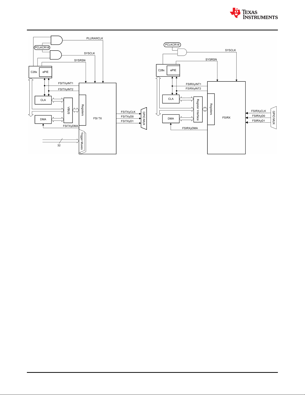
The FSI consists of the independent transmitter (FSITX) and receiver (FSIRX) cores, which are configured and
operated independently. Because of this, the FSI protocol does not have a notion of master and slave, unlike
some other synchronous communication protocols, and allows for simultaneous full speed communications in
both directions. Figure 1-1 shows the CPU interface of each FSI module. Each module owns up to three signal
lines: one clock and two data signals, where the second data lines, FSITXyD1 and FSIRXyD1, are optional, and
can be enabled for multi-lane transmission and double the speed for data bits. Thus, at least four signal lines are
needed to create 2-way point-to-point communication. Considering the timing spec for FSITX (see the devicespecific data sheets referenced in Section 7 ), the maximum data rate of 200 Mbps can be achieved with the
maximum clock of 50 MHz, using two data lines, since the data is transmitted on both edges of the clock signal.
For a full overview of FSI including all features and functions available, see the device-specific Technical
Reference Manual (TRM).
SPRACM3C – SEPTEMBER 2020 – REVISED OCTOBER 2020
Submit Document Feedback
Copyright © 2020 Texas Instruments Incorporated
Using the Fast Serial Interface (FSI) With Multiple Devices in an Application 3
Page 4
Introduction to the FSI Module
www.ti.com
Figure 1-1. FSITX and FSIRX CPU Interface
4 Using the Fast Serial Interface (FSI) With Multiple Devices in an Application SPRACM3C – SEPTEMBER 2020 – REVISED OCTOBER 2020
Copyright © 2020 Texas Instruments Incorporated
Submit Document Feedback
Page 5
www.ti.com
FSI Applications
2 FSI Applications
In terms of the trend in power electronic applications, the increasing demand for higher power levels makes
multiple power modules in parallel much more popular. Examples of such applications include industrial drives,
telecom rectifiers, server power supplies, on-board chargers, and so forth. Meanwhile, to achieve a complex
system with high performance, multiple MCUs are commonly used and must operate in a synchronized fashion.
Thus, critical data, including protection signals, sampling parameters, and even control loop data, needs to be
transferred with the fastest speed and least amount of latency among multiple devices/modules. FSI will be more
suitable to handle this when compared to the traditional Controller Area Network (CAN), Serial Peripheral
Interface (SPI) or Universal Asynchronous Receiver/Transmitter (UART).
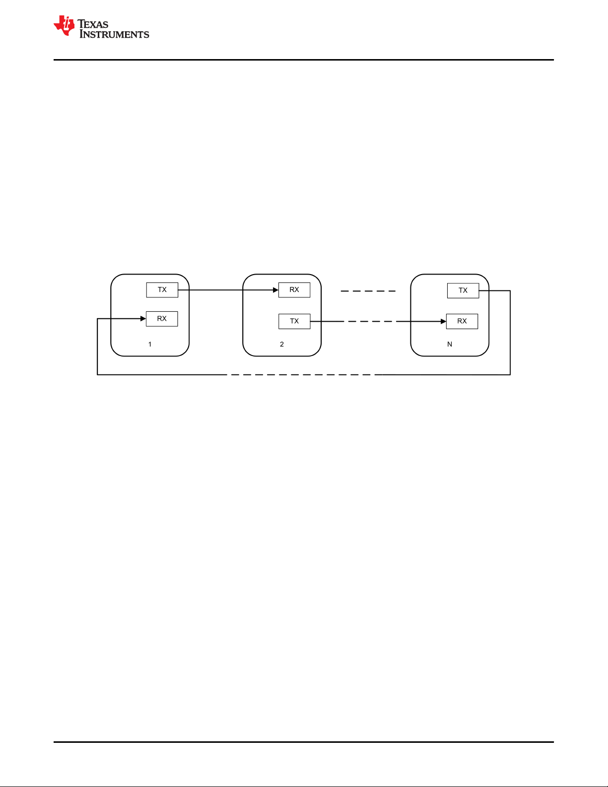
There are a number of communication network topologies for connecting multiple devices, each with their own
benefits. A ring topology can be created by connecting multiple devices with FSI communication in a daisy-chain
fashion. The advantages of a ring topology are that each device only needs one FSI transmitter and receiver and
also the simplicity from a physical connection perspective. Figure 2-1 shows a daisy-chain connection system for
N (N≥2) node devices, where each device (index i) connects with the FSITX of device i-1 and FSIRX of device i
+1.
Figure 2-1. Daisy-Chain Connection Example
One disadvantage of the above daisy-chain topology is that if one device in the chain fails then the entire
communication link is broken. Another downside is that devices must forward data along to the next device in the
chain if the received data is intended for a subsequent device. This can add to the overall latency of when a data
packet is transmitted and when the respective device in the chain receives the data.
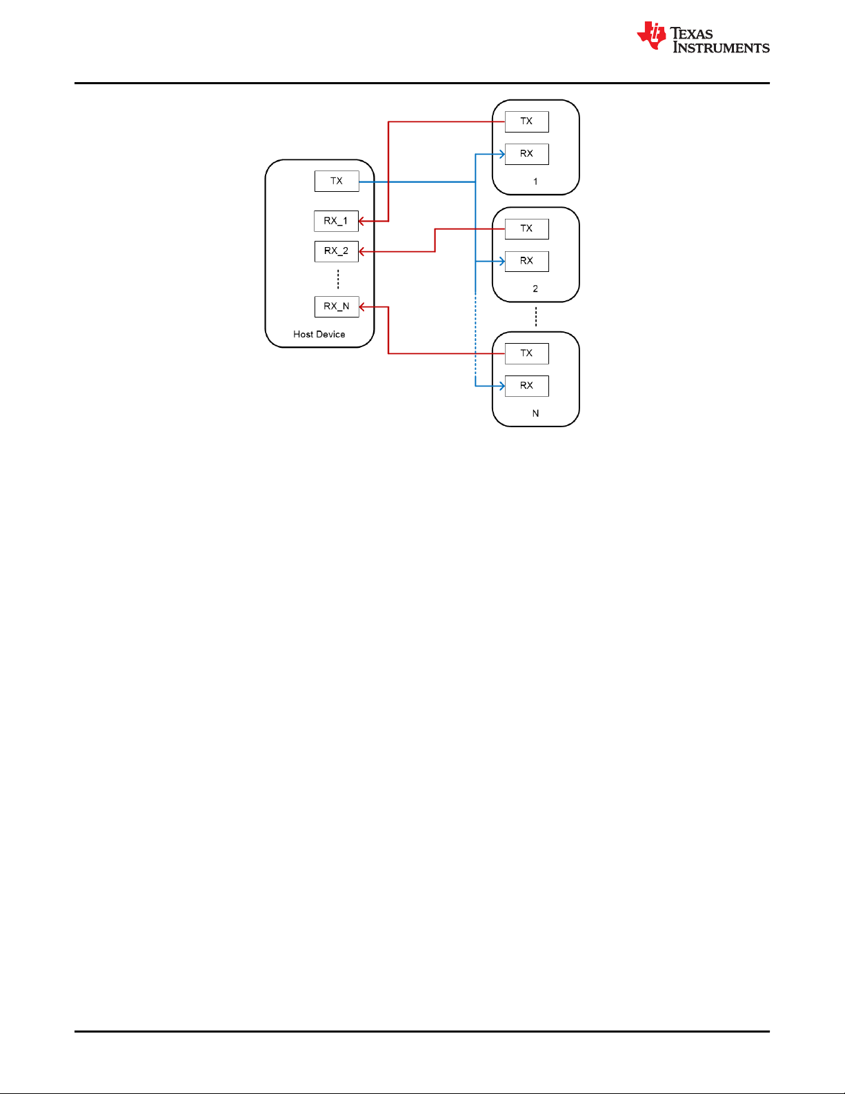
One communication topology that solves the broken link issue and can reduce the device-to-device latency is a
star topology, where several nodes connect directly to one central host device. Figure 2-2 shows a star topology
system with N (N≥2) node devices.
SPRACM3C – SEPTEMBER 2020 – REVISED OCTOBER 2020
Submit Document Feedback
Copyright © 2020 Texas Instruments Incorporated
Using the Fast Serial Interface (FSI) With Multiple Devices in an Application 5
Page 6
FSI Applications
www.ti.com
Figure 2-2. Star Topology Example
The host device's FSI transmitter is connected to the FSI receiver of each node device in order for the host to
broadcast data packets to all nodes simultaneously. The node device transmitter's, on the other hand, are
connected to independent receivers of the host device enabling them to send data directly back to the host at
any time. This star implementation comes with a resource cost as the host needs N number of independent FSI
receiver modules. The F2838x family of C2000 devices fit into the host socket with having two FSI transmitters
and eight FSI receivers.
6 Using the Fast Serial Interface (FSI) With Multiple Devices in an Application SPRACM3C – SEPTEMBER 2020 – REVISED OCTOBER 2020
Copyright © 2020 Texas Instruments Incorporated
Submit Document Feedback
Page 7

www.ti.com
Handshake Mechanism
3 Handshake Mechanism
A handshake mechanism can be implemented in order to configure the devices and validate the link in an FSI
communication topology. The different handshake sequences are discussed in the following sections.
3.1 Daisy-Chain Handshake Mechanism
Once the FSITX and FSIRX modules of each device have been configured, the handshake mechanism should
be implemented to prepare each device in the chain before actual data transmission, since devices may power
up in an arbitrary order in a real scenario.
In order to simplify the data flow, one device is assigned as the lead, working as the driver of the handshake
sequence, and the other N-1 devices, within the daisy-chain loop, are assigned as nodes. Following the example
in Figure 2-1, Device 1 will be the lead device. It should be noted that the other N-1 node devices will share the
same handshake configuration.
The handshake process can be described as follows:
1. For all devices, configure the Frame Type of FSITX as Ping Frame, and enable the receiver interrupts for
Ping Frame Received event on the FSI INT1 vector to detect the incoming transmission.
2. Begin the ping loop 0:
a. The lead device sends the flush sequence to the second device followed by a ping frame with Tag0(0000);
wait for some time. If the lead device receives a valid ping frame tag Tag0, continue to the second loop;
otherwise iterate the ping loop 0 again.
b. The node devices enter a wait loop for a receiver interrupt. If a valid ping frame tag of Tag0 is received
from the previous device, continue to the loop 1; otherwise iterate the ping loop 0 again.
3. Begin the ping loop 1:
a. The lead device sends a ping frame with Tag1(0001); wait for some time. If the lead device receives a
valid ping frame Tag1 the handshake sequence is complete and the application can continue; otherwise
iterate the ping loop 1 again.
b. The node devices send the flush sequence followed by a ping frame Tag0 and wait for a receiver interrupt.
If a valid ping frame Tag1 is received send a ping frame Tag1 to signal the completion of the handshake
sequence; or else iterate the ping loop 1 again.
4. Handshake completed.
SPRACM3C – SEPTEMBER 2020 – REVISED OCTOBER 2020
Submit Document Feedback
Copyright © 2020 Texas Instruments Incorporated
Using the Fast Serial Interface (FSI) With Multiple Devices in an Application 7
Page 8

Handshake Mechanism
www.ti.com
Figure 3-1. Daisy-Chain Handshake Sequence
The simplified data flow is shown in Figure 3-1. Two ping loops are necessary for the daisy-chain connection
handshake mechanism. Ping loop 0 has the purpose of establishing the communication path along the chain of
devices and ping loop 1 acts as the acknowledgment to the nodes that the communication path is good. In ping
loop 0, the node devices wait to receive a Ping Tag0 from the previous device in the chain. Once a Ping Tag0 is
successfully received, it will be forwarded on to the next device in the chain. The ping loop 0 will fail if a device in
the chain has not powered up or is not ready for the reception. Once ping loop 0 has succeeded, in which ping
tag0 has made its way back to the lead device, ping loop 1 is initiated to inform the node devices that the
handshake sequence has completed and to begin expecting actual data.
The handshake function can be found in the tested projects, with handshake_lead() for the lead device and
handshake_node() for the other N-1 devices in the daisy-chain loop.
8 Using the Fast Serial Interface (FSI) With Multiple Devices in an Application SPRACM3C – SEPTEMBER 2020 – REVISED OCTOBER 2020
Copyright © 2020 Texas Instruments Incorporated
Submit Document Feedback
Page 9

www.ti.com
Handshake Mechanism
3.2 Star Handshake Mechanism
A handshake sequence very similar to what's described in Section 3.1 can be applied for the star topology case.
In this implementation the host, or lead, device sends broadcast pings to all of the node devices and they each
respond along their independent TX paths. The lead device waits to receive ping frames from all nodes before
moving on to the next step. The sequence is shown below in Figure 3-2.
Figure 3-2. Star Handshake Sequence
SPRACM3C – SEPTEMBER 2020 – REVISED OCTOBER 2020
Submit Document Feedback
Copyright © 2020 Texas Instruments Incorporated
Using the Fast Serial Interface (FSI) With Multiple Devices in an Application 9
Page 10

Sending and Receiving FSI Data Frames
www.ti.com
4 Sending and Receiving FSI Data Frames
4.1 FSI Data Frame Configuration APIs
Several configurations are needed for data frames to be sent and received properly, including the frame type,
frame tag, user data, word length, number of data lines, and writing to or reading from the data buffer. The
configuration example code uses driverLib API functions for FSITX and FSIRX, defined in the fsi.h driverLib
header file in C2000WARE, which are shown below. Note that the content of frame tag and user data is fully
user-configurable, which can be used to differentiate which device the data received is sent from or which device
it is meant for.
// TX setting part
FSI_setTxFrameType(FSITXA_BASE, FSI_FRAME_TYPE_NWORD_DATA);
FSI_setTxSoftwareFrameSize(FSITXA_BASE, nWords);
FSI_setTxDataWidth(FSITXA_BASE, nLanes);
FSI_setTxUserDefinedData(FSITXA_BASE, txUserData);
FSI_setTxFrameTag(FSITXA_BASE, txDataFrameTag);
// RX setting part
FSI_setRxSoftwareFrameSize(FSIRXA_BASE, nWords);
FSI_setRxDataWidth(FSIRXA_BASE, nLanes);
4.2 Start Transmitting Data Frames
There are three methods to trigger the data transmission, including software triggered, externally triggered
(EPWMx-SOCA/B), or using the DMA. For the software triggering method, writing 1 to the
TX_FRAME_CTRL.START register bit, or using the driverLib function “FSI_startTxTransmit()”, will start the
transmission. If using an external trigger, like EPWMx-SOCA, once the external trigger signal occurs, the data
will be sent.
Since the DMA trigger can be generated every time a data frame transmission or receiving is completed from the
FSITX or FSIRX module, it provides a convenient method to transfer and store data, especially with a mass
amount of data. Here a configuration example is given for the FSI communication using DMA.
TX_OPER_CTRL_LO.START_MODE must be set to 0x2, which means writing to frame tag/user data fields can
trigger the transmission and then enables a DMA event on FSITX:
FSI_setTxStartMode(FSITXA_BASE, FSI_TX_START_FRAME_CTRL_OR_UDATA_TAG);
FSI_enableTxDMAEvent(FSITXA_BASE);
Two consecutive DMA channels are needed to fill the transmit buffer and frame tag/user data fields, respectively.
Using the two channels in sequence allows for the transmission to start right after the frame tag and user data
are set, as configured in the TX_OPER_CTRL_LO.START_MODE register bits. In the example code, DMA CH1
and DMA CH2 are used. Another important point is that the wrap control must be enabled for data of more than
16 words, since the FSI transmit buffer is a 16-word circular buffer.
DMA_configWrap(DMA_CH1_BASE, DMA_TRANSFER_SIZE_IN_BURSTS, 0, dest_WrapSize, 0);
Here, dest_WrapSize represents the number of bursts to be transferred before a wrap of the destination
address, so dest_WrapSize should be 16/ nWords. This can be implemented such that the transmit buffer is
continuously fed by the DMA, which is triggered by FSITX in return, with DMA Continuous Mode enabled.
The FSIRX is configured very similarly to the FSITX, except for that there is no order requirement for the DMA
channels for RX buffer and tag and user data. In the example projects, DMA CH3 and DMA CH4 are used.
10 Using the Fast Serial Interface (FSI) With Multiple Devices in an Application SPRACM3C – SEPTEMBER 2020 – REVISED OCTOBER 2020
Copyright © 2020 Texas Instruments Incorporated
Submit Document Feedback
Page 11

www.ti.com Daisy-Chain Topology Tests
5 Daisy-Chain Topology Tests
In order to demonstrate the communication speed and different configurations for FSI, daisy-chain connections
for two device and three device configurations have been tested and validated. The test hardware utilized is
composed of multiple F280025C ControlCARD Evaluation Modules and TMDSFSIADAPEVMs.
Note
These same tests can be performed with LAUNCHXL-F280049Cs and TMDSFSIADAPEVMs as well
with similar hardware setups.
The tested example projects can be found within the C2000WARE download. All test results were collected
using optimization level 2, configured within Code Composer Studio™ (CCS). Changing the optimization level
may yield different results. An overall description of the tested projects is shown in Table 5-1. For better
understanding, a general software flow chart with different project settings is shown in Figure 5-1.
Table 5-1. Example Projects Description - Daisy-Chain
Project Description Settings
fsi_ex_daisy_handshake_
lead
fsi_ex_daisy_handshake_
node
Project for the lead device in the daisy-chain
loop.
Project for the N-1 other devices (N>=2) in the
daisy-chain loop.
① [#define FSI_DMA_ENABLE 0] represents FSI
communication using CPU control.
② [#define FSI_DMA_ENABLE 1 && #define
TX_DMA_TRIGGER_ENABLE 0] represents FSI
communication using DMA control, and using software to
trigger DMA for the transmitted data (manually).
③ [#define FSI_DMA_ENABLE 1 && #define
TX_DMA_TRIGGER_ENABLE 1] represents FSI
communication using DMA control, and enabling FSITX
to trigger DMA for the transmitted data.
SPRACM3C – SEPTEMBER 2020 – REVISED OCTOBER 2020
Submit Document Feedback
Copyright © 2020 Texas Instruments Incorporated
Using the Fast Serial Interface (FSI) With Multiple Devices in an Application 11
Page 12

Daisy-Chain Topology Tests
www.ti.com
Figure 5-1. Software Flow Chart With Different Project Settings
12 Using the Fast Serial Interface (FSI) With Multiple Devices in an Application SPRACM3C – SEPTEMBER 2020 – REVISED OCTOBER 2020
Copyright © 2020 Texas Instruments Incorporated
Submit Document Feedback
Page 13
www.ti.com
Daisy-Chain Topology Tests
5.1 Two Device FSI Communication
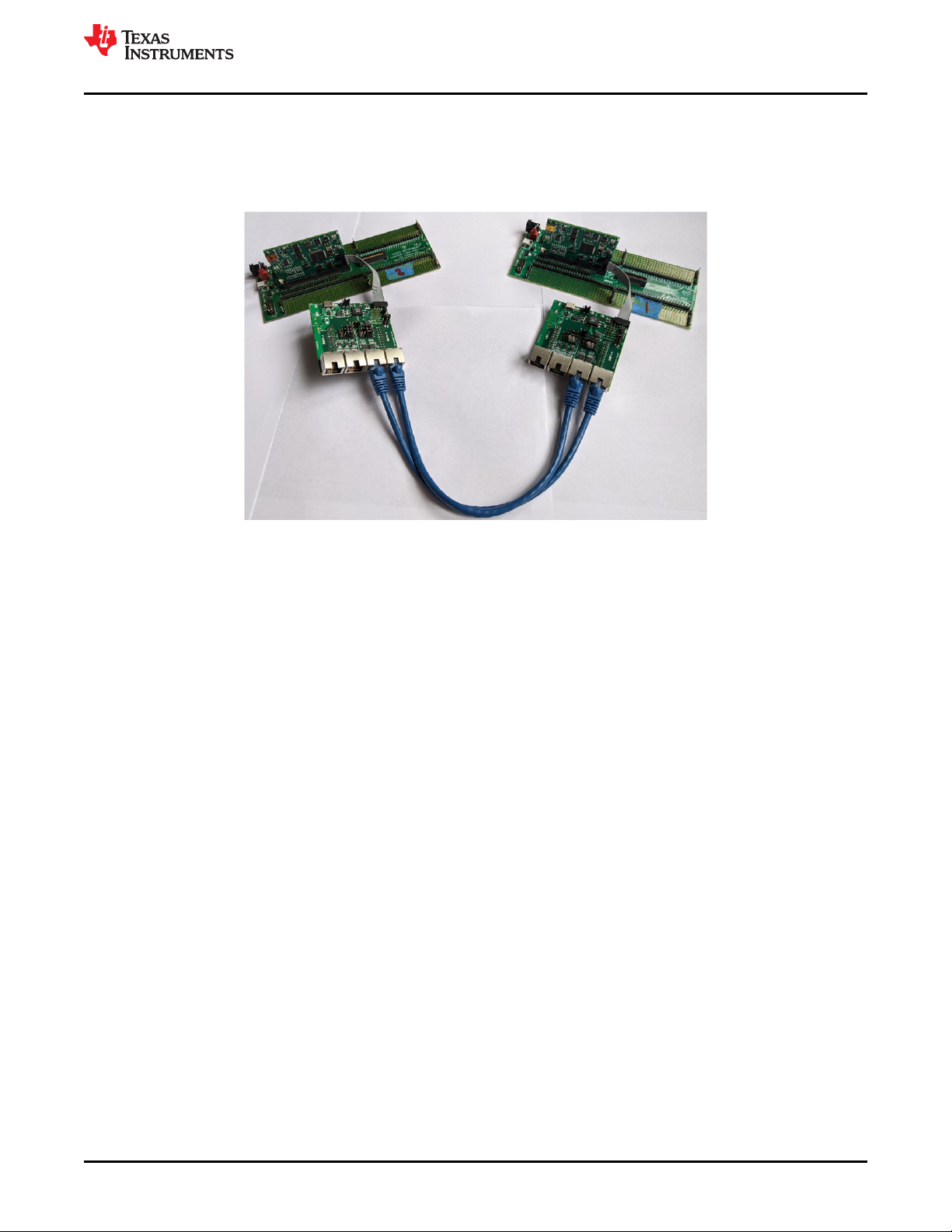
For a minimal daisy-chain connection test, a system of two F280025C ControlCARD Evaluation Modules and
TMDSFSIADAPEVMs are used as shown in Figure 5-2. The comparison of the communication speeds for both
CPU control and DMA control is provided in the following sub-sections.
Figure 5-2. Test Platform for Two Device Communication
5.1.1 CPU Control
• Test condition:
Device 1 sends data -> Device 2 receives data -> Device 2 CPU moves RX data to TX buffer and registers ->
Device 2 triggers FSI TX with SW which forwards the received data back to Device 1 -> Device1 receives data
back and the CPU verifies it matches the originally sent TX data.
• Test case:
Data length of 8 words, two data lines, TXCLK = 50 MHz, with Setting ① (Table 5-1) enabled.
In the test, GPIOs are toggled within software when specific events occur during the communication and
measured using an oscilloscope to obtain the respective timing data. In Figure 5-3, the green signal represents
the GPIO toggling of Device 1 (Lead device) and the magenta signal represents the GPIO toggling of Device 2
(Node device).
SPRACM3C – SEPTEMBER 2020 – REVISED OCTOBER 2020
Submit Document Feedback
Copyright © 2020 Texas Instruments Incorporated
Using the Fast Serial Interface (FSI) With Multiple Devices in an Application 13
Page 14

Daisy-Chain Topology Tests
www.ti.com
Figure 5-3. Data Transmission Test Using CPU Control
From the results shown in Figure 5-3, the time obtained for the data transmission is ~1.4 µs. In order to calculate
the transmission speed, the total data length should be considered. Table 5-2 shows the general structure of a
data frame, which can be divided into two parts: effective data bits and overhead bits.
• Effective Data Bits: Includes the 8-bit User Data, 16-bit Data Words, and 8-bit CRC fields
• Overhead Bits: Includes the Preamble, SOF, Frame Type, EOF, and Postamble fields
Therefore, the ideal transmission time for 8 words can be derived theoretically, as shown in Table 5-3.
It should be noted that since two data lines only work for effective data bits, one FSITXCLK cycle delivers 4
effective data bits, while one FSITXCLK cycle only delivers 2 overhead bits. Thus, with a total 48 FSITXCLK
cycles for 8 data words, the transmission time can be calculated as shown in Equation 1.
(FSITXCLK cycles) / (FSITXCLK frequency) = 48 /
(
50 M H z
) = 0 . 96 μ
s
(1)
Therefore, the theoretical transmission speed is 175 Mbps (168/0.96 µs), while the speed from the test is 120
Mbps with 1.4 µs transmission time, due to the fact that the tested transmission time includes entering the ISR
(to toggle an IO pin), delay introduced by isolators, transceivers, cables, and so forth. If changing to one data
line, the theoretical transmission speed is 100 Mbps, while the test speed is 80 Mbps with a transmission time of
2.1 µs.
Another finding from Figure 5-3 is that moving data from the FSIRX buffers to the FSITX buffers in the node
device takes some time, approximately 4.9 µs using the FSI driverLib functions. This will be a key factor that
distinguishes DMA control as shown in the next section.
Note
The time to move data between the FSI buffers and registers can be optimized by writing to and
reading from the FSI registers directly instead of using the provided driverLib functions.
14 Using the Fast Serial Interface (FSI) With Multiple Devices in an Application SPRACM3C – SEPTEMBER 2020 – REVISED OCTOBER 2020
Copyright © 2020 Texas Instruments Incorporated
Submit Document Feedback
Page 15

www.ti.com
Daisy-Chain Topology Tests
Table 5-2. Data Frame Structure
IDLE Preamble SOF
1111 1001 0011 8 bits N words 8 bits 4 bits 0110 1111
Frame
Type User Data
Data
Words CRC Frame Tag EOF Postamble IDLE
Table 5-3. Calculated Transmission Time for 8 Words
Effective Data Bits
(bits) Overhead Bits (bits) Total Length (bits)
144 24 168 36 12 0.96
FSITXCLK Cycles
for Effective Data
Bits (cycles)
FSITXCLK Cycles
for Overhead Bits
(cycles)
Total Data
Transmission Time
(us)
5.1.2 DMA Control
• Test condition
Device 1 sends data -> Device 2 receives data -> Device 2 DMA moves RX data to TX buffer and registers ->
Device 2 triggers TX when TX_FRAME_TAG_UDATA FSI register is written to which forwards the received
data back to Device 1 -> Device 1 receives data back -> Device 1 DMA moves RX data to memory -> CPU
verifies data in memory matches the originally sent TX data.
• Test case
Data length of 8 words (8 words per burst, 1 burst per transfer), two data lines, TXCLK = 50 MHz, with Setting ②
(Table 5-1) enabled.
In this test, DMA interrupts from CH2 and CH4 are enabled to trigger at the end of a transfer in the lead device,
which means that interrupts occur every time data has been copied from memory to the FSITX buffer (CH2) or
data has been transferred out of the FSRX buffer to a location in memory (CH4). In the node device, the DMA
channels are configured to transfer received data from the RX buffers and registers to the TX buffers and
registers anytime an FSI data frame is received, ultimately forwarding the data back to the lead device.
Therefore the node device only has one DMA interrupt enabled while the lead device has two. With GPIOs
toggling in the DMA ISRs, Figure 5-4 shows the test results of FSI communication using DMA control.
Figure 5-4. FSI Communication Using DMA Control
SPRACM3C – SEPTEMBER 2020 – REVISED OCTOBER 2020
Submit Document Feedback
Copyright © 2020 Texas Instruments Incorporated
Using the Fast Serial Interface (FSI) With Multiple Devices in an Application 15
Page 16

Daisy-Chain Topology Tests
www.ti.com
It should be noted that the time of 1.86 µs shown includes the time for the lead device to transmit the data frame,
the node device to move RX data to the TX buffer / registers, entering of the ISR, and toggling the GPIO.
According to the DMA pipeline timing requirements (See device specific TRM referenced in Section 7 for more
info), the time for moving data of 9 words (8 words data + 1 word of user data and frame tag) using 2 channels
can be calculated as shown in Equation 2.
( 9 × 3 c y c l e s / w o r d + 2 c y c l e s ) ÷ ( 100 M H z ) = 0 . 29 μ s (2)
Thus, considering other delay times, the actual transmission time is almost aligned with the former test result
(1.4 µs) using CPU control. Also, it should be highlighted that utilizing the DMA in this case drastically saves the
time for transferring received data, especially in an application with mass data transmissions..
Further test results are given in Table 5-4, for the comparison of using CPU control and DMA control of FSI. With
overhead bits being fixed in the FSI data frame structure, it is beneficial to use a longer data length to maximize
the effective data throughput.
Table 5-4. Comparison of Using CPU Control and DMA Control in FSI for Two Devices
CPU Control
DMA Control
FSITXCLK
(MHz) # of Data Lines
50 2 8 1.4 4.9 175 120
50 2 16 2.1 8.3 185 141
50 1 8 2.1 4.9 100 80
10 1 8 8.9 4.9 20 18.9
50 2 8 1.9 / /
50 2 16 3.0 / /
50 1 8 2.6 / /
10 1 8 9.3 / /
Data Length
(16-bit words)
Transmission
Time (µs)
(1)
Buffer Data
Move Time
(1)
(µs)
Theoretical
Transmission
Speed (Mbps)
Transmission
(2)
Speed (Mbps)
Test
(1) Measured times are rounded to the nearest 0.1 us.
(2) Accounts for FSI frame overhead bits being transmitted on both lines in the two data lines cases.
There may be cases where FSI communication may need some additional robustness and noise immunity and
for that reason a lower clock frequency has also been tested. The FSI protocol is designed to communicate only
when there is data exchange. This helps to reduce power and over all EMI in the system. Additionally, lower FSI
clock frequencies and half-duplex communication could improve overall system level EMI performance while
continuing to provide higher throughput than generic serial ports at the same operating frequencies. Generally, it
is best to use a twisted pair or shielded wire per line for board-to-board connections, while on board FSI signal
trace lengths should match and have special care taken in the layout to enhance noise immunity.
In the tests performed there are isolation and differential transceiver devices being used on the
TMDSFSIADAPEVM boards, which could introduce channel-to-channel skew. In a real world application that
utilizes these same or similar devices, and/or varying signal trace lengths, the integrated skew compensation
block within the FSI receiver module can be used to manage the skew that may occur between the clock and
data signals. For more information on this topic, see Fast Serial Interface (FSI) Skew Compensation.
16 Using the Fast Serial Interface (FSI) With Multiple Devices in an Application SPRACM3C – SEPTEMBER 2020 – REVISED OCTOBER 2020
Copyright © 2020 Texas Instruments Incorporated
Submit Document Feedback
Page 17

www.ti.com
Daisy-Chain Topology Tests
5.2 Three Device FSI Communication
Based on the test and comparison results given in Section 5.1, FSI communication for three devices has also
been investigated. The test platform used is shown in Figure 5-5.
Figure 5-5. Test Platform for Three Devices Communication
Due to the nature of a daisy-chain connection, data will need to pass through a number of devices for the
transmission from the first device to reach the last device. Therefore, to reduce latency it is important to make
the data handling and forwarding time in each device as short as possible, especially when there are a number
of devices in a connection loop. From the conclusion drawn in Section 5.1, to avoid having the CPU spending
too much bandwidth moving data, it is recommended to use the DMA to serve FSI communication. The following
tests utilize the same software discussed in Section 5 for the lead and node devices.
• Test condition
Device 1 sends data -> Device 2 receives data -> Device 2 moves RX data to TX buffer and sends data to
Device 3->…..-> Device 3 moves RX data to TX buffer and sends data to Device 1 -> Device1 receives data
and verifies the data matches the originally sent TX data.
• Test case
Data length of 8 words, 1 data line, TXCLK = 50 MHz, with setting ① for CPU control case and ② for DMA
control case (Table 5-1) enabled.
In the tests, GPIOs are toggled within software when specific events occur during the communication and
measured using an oscilloscope to obtain the respective timing data. In the figures below, the green signal
represents the GPIO toggling of Device 1 (Lead device), the blue signal represents the GPIO toggling of Device
2 (Node device), and the magenta signal represents the GPIO toggling of Device 3 (Node device).
SPRACM3C – SEPTEMBER 2020 – REVISED OCTOBER 2020
Submit Document Feedback
Copyright © 2020 Texas Instruments Incorporated
Using the Fast Serial Interface (FSI) With Multiple Devices in an Application 17
Page 18

Daisy-Chain Topology Tests
Figure 5-6. FSI Communication With CPU Control Among Three Devices
www.ti.com
Figure 5-7. Time of Data Going Through One Device - CPU Control
For the CPU control case, the time needed for the data transmission to complete the three device daisy-chain
loop is 16.2 µs, as shown in Figure 5-6. This time will increase by 7.1 us for each device added to the daisychain connection system, as shown in Figure 5-7. The 7.1 µs increased time per device includes the time for
transmission and moving RX data to the TX buffer and registers.
18 Using the Fast Serial Interface (FSI) With Multiple Devices in an Application SPRACM3C – SEPTEMBER 2020 – REVISED OCTOBER 2020
Copyright © 2020 Texas Instruments Incorporated
Submit Document Feedback
Page 19

www.ti.com
Daisy-Chain Topology Tests
Figure 5-8. FSI Communication with DMA Control Among Three Devices
Figure 5-9. Time of Data Going Through One Device - DMA Control
For the DMA control case, the time needed for the data transmission to complete the three device daisy-chain
loop is 6.5 µs, as shown in Figure 5-8. This time will increase by 2.3 us for each device added to the daisy-chain
connection system, as shown in Figure 5-9. The 2.3 µs increased time per device includes the time for
transmission and moving RX data to the TX buffer and registers.
SPRACM3C – SEPTEMBER 2020 – REVISED OCTOBER 2020
Submit Document Feedback
Copyright © 2020 Texas Instruments Incorporated
Using the Fast Serial Interface (FSI) With Multiple Devices in an Application 19
Page 20

Star Topology Tests
www.ti.com
Further test results can be found in Table 5-5.
Table 5-5. Comparison of Using CPU Control and DMA Control in FSI Among Three Devices
CPU control
DMA control
FSITXCLK (MHz) # of Data Lines
50 1 8 7.1 16.2
50 1 16 11.8 26.8
50 1 8 2.3 6.5
50 1 16 4.0 11.8
Data Length (16-bit
words)
Time of data going
through one device
(µs)
Time of the full
connection loop - 3
devices (us)
6 Star Topology Tests
The star topology over FSI application example demonstrates a different kind of communication topology,
showcasing how a central host device can receive information from multiple node devices at the same time
rather than wait for packets to be forwarded through subsequent devices, like in the daisy-chain example. The
advantages and disadvantages of the star topology are discussed in Section 2.
The defining requirements of the star implementation provided are hardware related, i.e. host device TX needing
to have multi-drop functionality to each node, and MCU resource related, i.e. host device needing N number of
RX instances. From a software perspective the central host device uses a new star_broadcast project while the
N node devices use the same node device software utilized in the daisy-chain tests, details provided in Table
6-1.
Table 6-1. Software Example Projects - Star Topology
Project Description Supported Devices
fsi_ex_star_broadcast Project for central host device in the star network F2838x
fsi_ex_daisy_handshake_node Project for N number of node devices in the star network F28002x, F28004x, F2838x
The software flow of the star_broadcast project is similar to that of the lead device CPU Control daisy-chain
project discussed in Section 5. The handshake mechanism will be slightly different as shown in Section 3.2.
Upon completion of the handshake, the central host device will transmit a broadcast data frame to all of the node
devices connected to its FSITX. The host will then wait to receive the data frame back from all connected node
devices and then validate that each received frame matches the originally transmitted one, after which it will
prepare and send a new data frame.
By default, the star_broadcast project has pre-made configurations for FSI RX instances A, B and C of the
device. Each instance can be configured by setting the individual pre-processor directives below to "1".
Additional FSI RX instances can be added if they are available on the host device.
//
// Enable FSI RX Instances
//
#define FSI_RXA_ENABLE 1
#define FSI_RXB_ENABLE 0
#define FSI_RXC_ENABLE 1
Timing measurements of the star topology will be very similar, if not the same, as those collected in the previous
daisy-chain tests. Therefore the data provided in Table 5-4 can be utilized for this purpose.
20 Using the Fast Serial Interface (FSI) With Multiple Devices in an Application SPRACM3C – SEPTEMBER 2020 – REVISED OCTOBER 2020
Copyright © 2020 Texas Instruments Incorporated
Submit Document Feedback
Page 21

www.ti.com
References
7 References
• Texas Instruments: TMS320F28002x Microcontrollers Data Sheet
• Texas Instruments: TMS320F28002x Microcontrollers Technical Reference Manual
• Texas Instruments: TMS320F2838x Microcontrollers Data Sheet
• Texas Instruments: TMS320F2838x Microcontrollers Technical Reference Manual
• Texas Instruments: TMS320F28004x Microcontrollers Data Sheet
• Texas Instruments: TMS320F28004x Microcontrollers Technical Reference Manual
• Texas Instruments: TIDM-02006 Distributed multi-axis servo drive over fast serial interface (FSI) reference
design
• Texas Instruments: Distributed Power Control Architecture With Multiple MCUs Over FSI
• TMDSFSIADAPEVM: FSI Adapter Board
• F280025C ControlCARD Evaluation Modules
8 Revision History
NOTE: Page numbers for previous revisions may differ from page numbers in the current version.
Changes from September 00, 2020 to October 12, 2020 (from Revision B (September 2020) to
Revision C (October 2020)) Page
• Updates were made in the Abstract................................................................................................................0
• Updated the numbering format for tables, figures and cross-references throughout the document...................3
• Update was made to Section 1...........................................................................................................................3
SPRACM3C – SEPTEMBER 2020 – REVISED OCTOBER 2020
Submit Document Feedback
Copyright © 2020 Texas Instruments Incorporated
Using the Fast Serial Interface (FSI) With Multiple Devices in an Application 21
Page 22

IMPORTANT NOTICE AND DISCLAIMER
TI PROVIDES TECHNICAL AND RELIABILITY DATA (INCLUDING DATASHEETS), DESIGN RESOURCES (INCLUDING REFERENCE
DESIGNS), APPLICATION OR OTHER DESIGN ADVICE, WEB TOOLS, SAFETY INFORMATION, AND OTHER RESOURCES “AS IS”
AND WITH ALL FAULTS, AND DISCLAIMS ALL WARRANTIES, EXPRESS AND IMPLIED, INCLUDING WITHOUT LIMITATION ANY
IMPLIED WARRANTIES OF MERCHANTABILITY, FITNESS FOR A PARTICULAR PURPOSE OR NON-INFRINGEMENT OF THIRD
PARTY INTELLECTUAL PROPERTY RIGHTS.
These resources are intended for skilled developers designing with TI products. You are solely responsible for (1) selecting the appropriate
TI products for your application, (2) designing, validating and testing your application, and (3) ensuring your application meets applicable
standards, and any other safety, security, or other requirements. These resources are subject to change without notice. TI grants you
permission to use these resources only for development of an application that uses the TI products described in the resource. Other
reproduction and display of these resources is prohibited. No license is granted to any other TI intellectual property right or to any third
party intellectual property right. TI disclaims responsibility for, and you will fully indemnify TI and its representatives against, any claims,
damages, costs, losses, and liabilities arising out of your use of these resources.
TI’s products are provided subject to TI’s Terms of Sale (www.ti.com/legal/termsofsale.html) or other applicable terms available either on
ti.com or provided in conjunction with such TI products. TI’s provision of these resources does not expand or otherwise alter TI’s applicable
warranties or warranty disclaimers for TI products.
Mailing Address: Texas Instruments, Post Office Box 655303, Dallas, Texas 75265
Copyright © 2020, Texas Instruments Incorporated
 Loading...