

®
0
4
7
0
1
A
SBOS214B – SEPTEMBER 2001 – REVISED JULY 2004
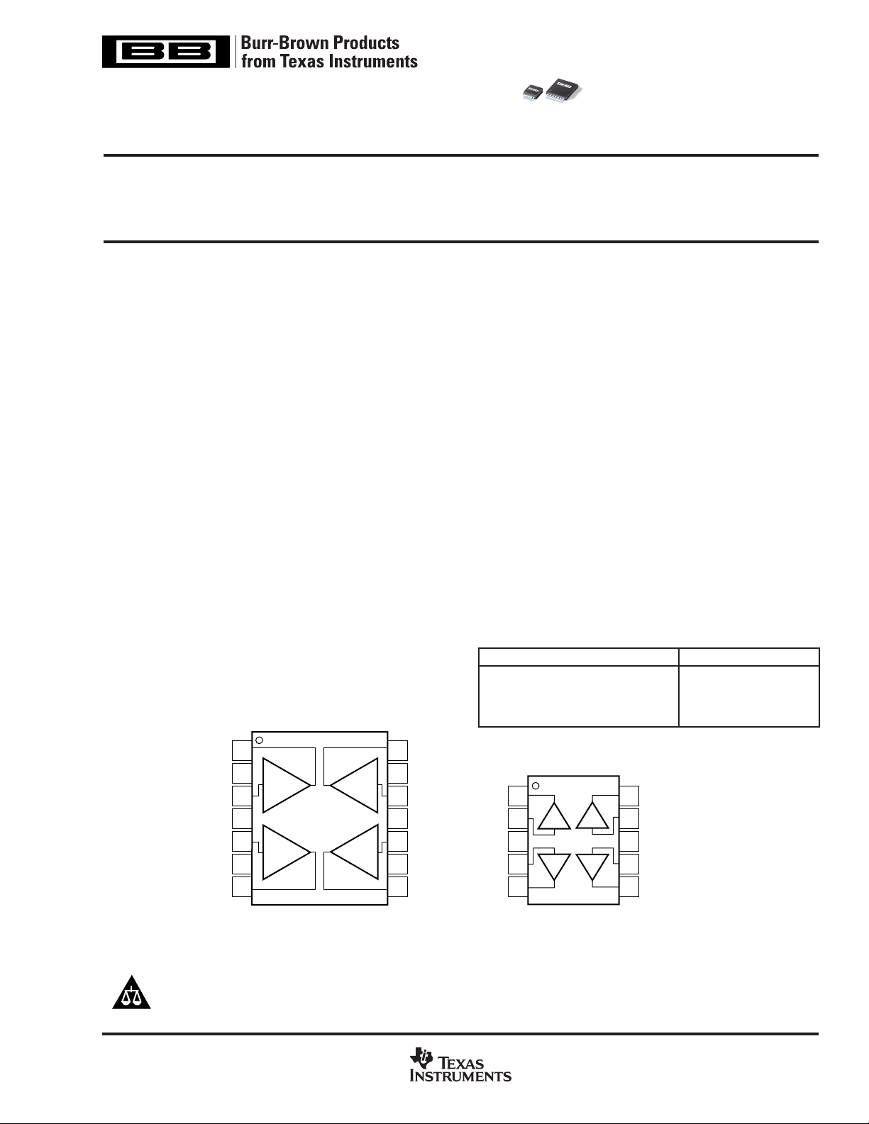
4-Channel, Rail-to-Rail, CMOS
BUFFER AMPLIFIER
BUF04701
FEATURES
● UNITY GAIN BUFFER
● RAIL-TO-RAIL INPUT/OUTPUT
● WIDE BANDWIDTH: 8MHz
● HIGH SLEW RATE: 10V/µs
● LOW QUIESCENT CURRENT: 1.1mA
● TINY PACKAGE: MSOP-10, TSSOP-14
APPLICATIONS
● TFT-LCD REFERENCE DRIVERS
● NOTEBOOKS
● ELECTRONIC GAMES
● ELECTRONIC BOOKS
● PERSONAL COMMUNICATION DEVICES
● PDA
● ACTIVE FILTERS
● ADC/DAC BUFFER
DESCRIPTION
The BUF04701 is a 4-channel, low-power, high-voltage railto-rail input/output buffer. Operating on supplies ranging from
3.5V to 12V (±1.75V to ±6V), the BUF04701 has a 3dB
bandwidth of 8MHz with a slew rate of 10V/µs, and requires
only 1.1mA quiescent current. The BUF04701 features railto-rail input and output capability, giving maximum dynamic
range at any supply voltage.
Featuring fast slewing and settling times, as well as a high
output drive, the BUF04701 is ideal for use as a voltage
reference buffer in Thin Film Transistor Liquid Crystal Displays (TFT-LCDs).
The BUF04701 is available in an MSOP-10 package, providing the smallest footprint and thinnest package option available, as well as the TSSOP-14 package with a pinout that
corresponds to standard quad op amps. This makes it easy to
replace quad op amps in existing LCD displays with the low
cost BUF04701, without changing the layout. The BUF04701
operates over a temperature range of –40°C to +125°C.
BUF04701 RELATED PRODUCTS
FEATURES PRODUCT
1.2 MHz BW, 3.3mA I
7MHz GBW, 1.5mA IQ, VS 3.5 - 12 OPA4743
5.9MHz GBW, 4.5mA I
10MHz GBW, 2.5mA I
Q
, VS = 4V - 44V TLE2144/2
Q
, 16V/µs SR TLC084
Q
BUF11702
1
Out A
(1)
2
NC
In A
+V
In B
NC
Out B
(1)
AC
3
4
5
BD
6
7
TSSOP-14 (PW)
NOTE: (1) NC Means No Internal Connection
Please be aware that an important notice concerning availability, standard warranty, and use in critical applications of
Texas Instruments semiconductor products and disclaimers thereto appears at the end of this data sheet.
All trademarks are the property of their respective owners.
PRODUCTION DATA information is current as of publication date.
Products conform to specifications per the terms of Texas Instruments
standard warranty. Production processing does not necessarily include
testing of all parameters.
14
13
12
11
10
9
8
Out D
(1)
NC
In D
–V
In C
(1)
NC
Out C
www.ti.com
Out A
In A
+V
In B
Out B
1
2
3
4
5
MSOP-10 (DGS)
Out D
10
In D
9
–V
8
In C
7
Out C
6
Copyright © 2001-2004, Texas Instruments Incorporated

ABSOLUTE MAXIMUM RATINGS
Supply Voltage, V+ to V–................................................................. 13.2V
Signal Input Terminals, Voltage
Output Short-Circuit
Operating Temperature .................................................. –40°C to +125°C
Storage Temperature ..................................................... –65°C to +150°C
Junction Temperature .................................................................... +150°C
Lead Temperature (soldering, 10s)............................................... +300°C
NOTES: (1) Stresses above these ratings may cause permanent damage.
Exposure to absolute maximum conditions for extended periods may
degrade device reliability. (2) Input terminals are diode-clamped to the
power-supply rails. Input signals that can swing more than 0.5V beyond the
supply rails should be current-limited to 10mA or less. (3) Short-circuit to
ground, one amplifier per package.
(3)
(2)
................... (V–) –0.5V to (V+) + 0.5V
(2)
Current
.............................................................. Continuous
.................................................... 10mA
(1)
ELECTROSTATIC
DISCHARGE SENSITIVITY
This integrated circuit can be damaged by ESD. Texas Instruments recommends that all integrated circuits be handled with
appropriate precautions. Failure to observe proper handling
and installation procedures can cause damage.
ESD damage can range from subtle performance degradation to complete device failure. Precision integrated circuits
may be more susceptible to damage because very small
parametric changes could cause the device not to meet its
published specifications.
PACKAGE/ORDERING INFORMATION
PRODUCT PACKAGE-LEAD DESIGNATOR RANGE MARKING NUMBER MEDIA, QUANTITY
Quad
BUF04701 MSOP-10 DGS –40°C to +125°C BUF04701 BUF04701AIDGSR Tape and Reel, 2500
BUF04701 TSSOP-14 PW –40°C to +125°C 04701A BUF04701AIPWR Tape and Reel, 2500
NOTE: (1) For the most current package and ordering information, see the Package Option Addendum located at the end of this data sheet.
(1)
SPECIFIED
PACKAGE TEMPERATURE PACKAGE ORDERING TRANSPORT
2
www.ti.com
BUF04701
SBOS214B
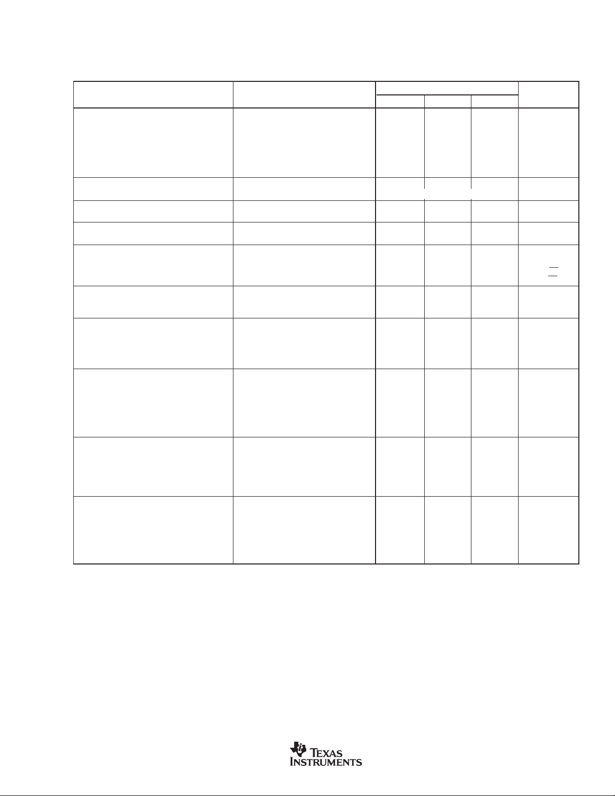
ELECTRICAL CHARACTERISTICS: VS = +3.5V to +12V
Boldface limits apply over the specified temperature range, TA = –40°C to +125°C
At TA = +25°C, RL = 10kΩ connected to VS/ 2 and V
PARAMETER CONDITION MIN TYP MAX UNITS
OFFSET VOLTAGE
Input Offset Voltage V
Drift dV
vs Power Supply PSRR V
/dT ±8 µV/°C
OS
Over Temperature V
Channel Separation, DC 1 µV/V
f = 10kHz 110 dB
INPUT VOLTAGE RANGE
Common-Mode Voltage Range V
INPUT BIAS CURRENT
Input Bias Current I
INPUT IMPEDANCE
Common-Mode 5 • 10
NOISE
Input Voltage Noise, f = 0.1Hz to 10Hz V
Input Voltage Noise Density, f = 10kHz e
Input Current Noise Density, f = 1kHz i
TRANSFER CHARACTERISTIC
Gain 0.9975 1.000 1.0025
over Temperature 0.995 1.000 1.005
OUTPUT
Voltage Output Swing from Rail R
over Temperature R
Short-Circuit Current I
FREQUENCY RESPONSE C
Bandwidth –3dB BW 8 MHz
Slew Rate SR V
Settling Time, 0.1% t
Overload Recovery Time V
Total Harmonic Distortion + Noise THD+N V
POWER SUPPLY
Specified Voltage Range, Single Supply V
Specified Voltage Range, Dual Supplies ±1.75 ±6V
Operating Voltage Range +3.5 to +12 V
Quiescent Current (per amplifier) I
over Temperature 1.7 mA
TEMPERATURE RANGE
Specified Range –40 +125 °C
Operating Range –40 +125 °C
Storage Range –65 +150 °C
Thermal Resistance
θ
TSSOP Surface Mount 100 °C/W
MSOP Surface Mount 200 °C/W
= VS/2, unless otherwise noted.
OUT
OS
CM
B
n
n
VS = ±5, VCM = 0 ±1.5 ±7mV
= 3.5V to 12V, VCM = VS/2 – 0.5V 20 100 µV/V
S
= 3.5V to 12V, VCM = VS/2 – 0.5V 200 µV/V
S
VCM = VS/2 1 ±10 pA
= ±6V, VCM = 0 11 µVrms
S
VS = ±6V, VCM = 0 30 nV/√Hz
VS = ±6V, VCM = 0 2.5 fA/√Hz
R
SC
S
S
Q
JA
VS = ±6V, 5V Step 9 µs
= ±6V, VO = 1Vrms, G = 1, 0.001 %
S
f = 6kHz, V
BUF04701
Limited by Output Range
12
|| 4 Ω || pF
= 10kΩ 75 mV
L
= 2kΩ 150 200 mV
L
= 2kΩ 250 mV
L
= 10pF
L
= ±6V 10 V/µs
S
= V
IN
S
= VS/2
CM
±32 mA
0.2 µs
3.5 12 V
IO = 0 1.1 1.5 mA
BUF04701
SBOS214B
www.ti.com
3
TYPICAL CHARACTERISTICS
At TA = +25°C, VS = ±6V, and RL = 10kΩ, unless otherwise noted.
120
V+
100
V–
80
60
PSRR (dB)
40
20
0
10 100 1k 10k 100k 1M
140
120
100
80
PSRR vs FREQUENCY
Frequency (Hz)
CHANNEL SEPARATION vs FREQUENCY
7
6
5
4
3
Amplitude (V)
2
1
0
10 100 1k 10k 100k 1M 10M
10k
1k
100
MAXIMUM AMPLITUDE vs FREQUENCY
VS = ± 6V
Frequency (Hz)
INPUT CURRENT AND VOLTAGE SPECTRAL
NOISE vs FREQUENCY
10k
1k
100
60
40
Channel Separation (dB)
20
0
10 100 1k 10k 100k 1M 10M
Frequency (Hz)
20
10
CL = 10pF
0
Gain (dB)
–10
–20
10k 100k 1M 10M 100M
GAIN vs FREQUENCY
RL = 10kΩ
R
C
L
L
RL = 200Ω
RL = 100Ω
Frequency (Hz)
RL = 1kΩ
RL = 500Ω
R
= 350Ω
L
10
Voltage Noise (nV/√Hz)
1
0.1
0.1 1 10 100 1k 10k 100k 1M
Frequency (Hz)
20
10
RL = 200Ω
0
Gain (dB)
–10
–20
10k 100k 1M 10M 100M
GAIN vs FREQUENCY
R
C
L
L
Frequency (Hz)
CL = 1000pF
CL = 500pF
= 100pF
C
L
CL = 10pF
10
1
0.1
Current Noise (fA/√Hz)
4
www.ti.com
BUF04701
SBOS214B
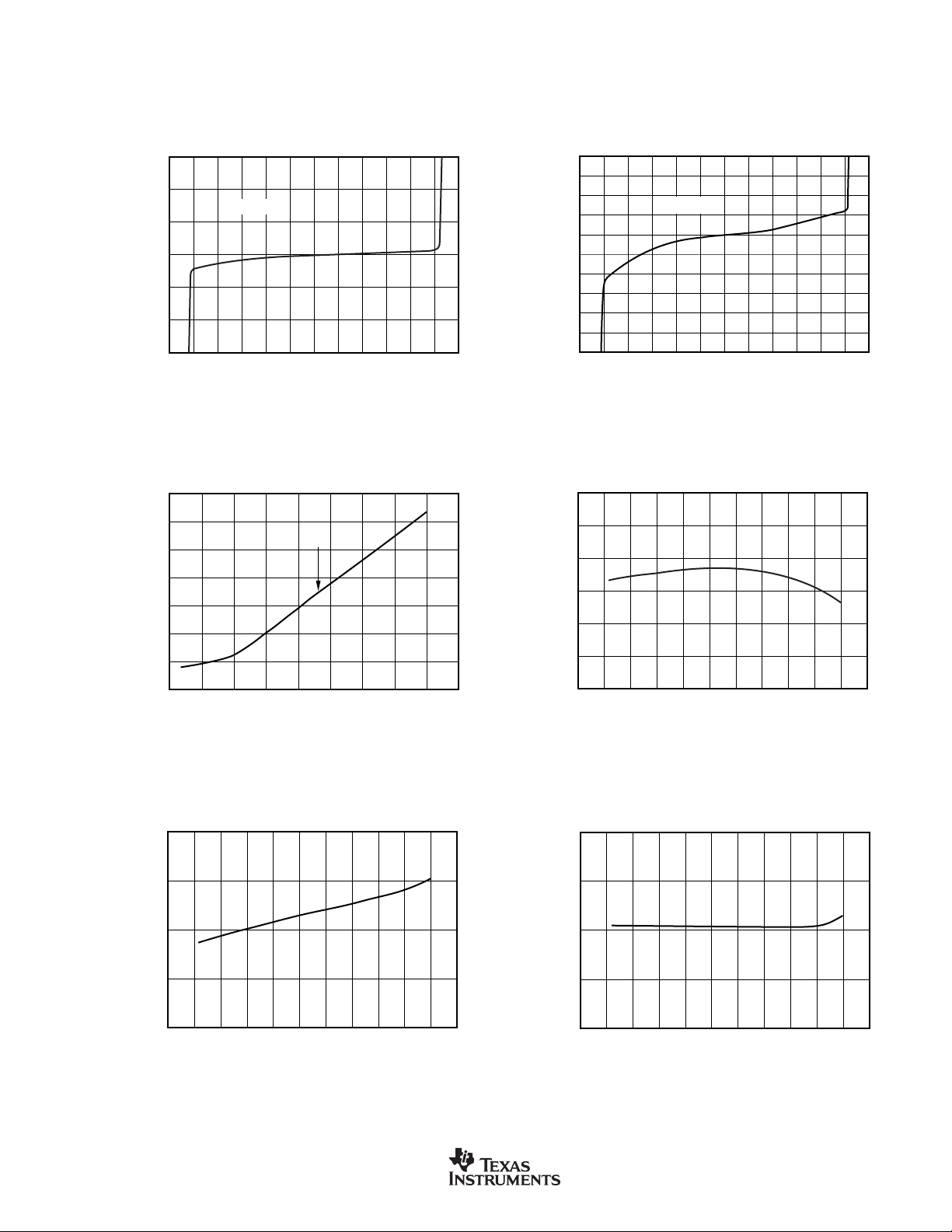
TYPICAL CHARACTERISTICS (Cont.)
120
110
100
90
80
70
60
–100 –75 –50 –25 0 25 50 75 100 125 150 175
PSRR vs TEMPERATURE
PSRR (dB)
Temperature (°C)
At TA = +25°C, VS = ±6V, and RL = 10kΩ, unless otherwise noted.
INPUT BIAS CURRENT (I
15
10
5
0
(pA)
B
I
–5
–10
–15
–6 –5 –4 –3 –2 –10 1 2 3 4 5 6
100k
10k
1k
100
VOLTAGE (V
INPUT BIAS (I
CM
VS = ±5V
vs TEMPERATURE
) vs COMMON-MODE
B
) TEMPERATURE = 25ºC
VCM (V)
) AND CURRENT
B
I
B
INPUT BIAS CURRENT (IB) vs COMMON-MODE
500
400
300
200
100
0
(pA)
B
I
–100
–200
–300
–400
–500
–6 –5 –4 –3 –2 –1
VOLTAGE (V
VS = ±5V
) TEMPERATURE = 85°C
CM
0
123456
VCM (V)
10
Bias Current (pA)
1.0
0.1
0.01
–50 –25 0 25 50 75 100 125 150 175
Temperature (°C)
2.0
1.5
1.0
per Amplitude (mA)
Q
0.5
I
0.0
–100 –75 –50 –25 0 25 50 75 100 125 150 175
QUIESCENT CURRENT vs TEMPERATURE
Temperature (°C)
1.005
1.000
Gain (V/V)
0.995
–100 –50 0 50 100 150 ??
GAIN vs TEMPERATURE
Temperature (°C)
BUF04701
SBOS214B
www.ti.com
5

TYPICAL CHARACTERISTICS (Cont.)
At TA = +25°C, VS = ±6V, and RL = 10kΩ, unless otherwise noted.
0.1
0.01
THD+N (%)
0.001
0.0001
50
40
30
20
(Gain = ±1 V/V, V
THD+N vs FREQUENCY
1 10 100 1k 10k 100k
SHORT-CIRCUIT CURRENT vs TEMPERATURE
Sinking
= 1.0Vrms, BW = 80kHz)
OUT
RL = 10kΩ
Frequency (Hz)
Sourcing
2.0
1.5
1.0
per Amplifier (mA)
Q
I
0.5
0.0
50
40
30
20
QUIESCENT CURRENT vs SUPPLY VOLTAGE
2 3 4 5 6 7 8 9 10 11 12 13 14
Supply Voltage (V)
SHORT-CIRCUIT CURRENT vs SUPPLY VOLTAGE
Sourcing
Sinking
10
Short-Circuit Current (mA)
0
–100 –75 –50 –25 0 25 50 75 100 125 150 175
Temperature (°C)
OUTPUT VOLTAGE SWING vs OUTPUT CURRENT
–4.5
–5.0
–5.5
Output Voltage (V)
–6.0
0 5 10 15
(Sinking)
125°C
Output Current (mA)
25°C
–40°C
85°C
10
Short-Circuit Current (mA)
0
2 3 4 5 6 7 8 9 10 11 12 13 14
Supply Voltage (V)
OUTPUT VOLTAGE SWING vs OUTPUT CURRENT
6.0
5.5
5.0
Output Voltage (V)
4.5
0 5 10 15
(Sourcing)
Output Current (mA)
25°C
–40°C
85°C
125°C
6
www.ti.com
BUF04701
SBOS214B

TYPICAL CHARACTERISTICS (Cont.)
SMALL SIGNAL STEP RESPONSE
(G = +1V/V, R
L
= 10kΩ, CL = 15pF)
10mV/div
100ns/div
At TA = +25°C, VS = ±6V, and RL = 10kΩ, unless otherwise noted.
100
90
80
70
60
50
40
Overshoot (%)
30
20
10
0
10 100 1k 10k
30
25
20
15
OVERSHOOT (%) vs CAPACITANCE
Load Capacitance Value (pF)
VOS DRIFT DISTRIBUTION
15
10
Frequency (%)
5
0
–7.0
–6.0
VOS PRODUCTION DISTRIBUTION
0
1.0
–5.0
–4.0
–3.0
–2.0
Voltage Offset (mV)
–1.0
2.0
3.0
4.0
5.0
6.0
7.0
8.0
Frequency (%)
10
5
0
–50
–40
–30
0
10
–20
–10
Voltage Offset Drift (µV/°C)
20
2V/div
30
40
50
60
LARGE SIGNAL STEP RESPONSE
(G = +1V/V, R
= 10kΩ, CL = 15pF)
L
1µs/div
BUF04701
SBOS214B
www.ti.com
7

APPLICATIONS INFORMATION
Figure 1 shows the BUF04701 connected as a buffer. Power
supplies should be bypassed with capacitors connected
close to the device pins. Capacitor values as low as 0.1µF
will assure stable operation in most applications, but high
output current and fast output slewing can demand large
current transients from the power supplies.
Rail-to-rail input and output swing helps maintain dynamic
range, especially in low supply applications. Figure 2 shows
the input and output waveforms for the BUF04701. On a ±6V
supply with a 100kΩ load connected to V
tested to swing within 50mV to the rail.
OPERATING VOLTAGE
The BUF04701 is fully specified and tested from 3.5V to 12V
over a temperature range of –40°C to +125°C. Parameters
that vary significantly with operating voltages or temperature
are shown in the Typical Characteristic Curves.
V+
0.1µF
V
IN
BUF04701
0.1µF
1/4
/2, the output is
S
R
L
RAIL-TO-RAIL INPUT
The input common-mode voltage range of the BUF04701
extends 100mV beyond the supply rails at room temperature;
however, due to the fixed gain at G = 1, the output will
limit the useable input range. This wide swing is achieved
with a complementary input stage—an N-channel input
differential pair in parallel with a P-channel differential pair.
The N-channel pair is active for input voltages close to the
positive rail, typically (V+) – 2.0V to 100mV above the
positive supply, while the P-channel pair is on for inputs
from 100mV below the negative supply to approximately
(V+) – 1.5V. There is a small transition region, typically
(V+) – 2.0V to (V+) – 1.5V, in which both pairs are on. This
500mV transition region can vary ±100mV with process
variation. Thus, the transition region (both stages on) can
range from (V+) – 2.1V to (V+) – 1.4V on the low end, up to
(V+) – 1.9V to (V+) – 1.6V on the high end.
INPUT PROTECTION
Device inputs are protected by ESD diodes that will conduct
if the input voltages exceed the power supplies by more than
approximately 300mV. Momentary voltages greater than
300mV beyond the power supply can be tolerated if the
current is limited to 10mA. This is easily accomplished with
an input resistor, in series with the buffer input shown in
Figure 3. Many input signals are inherently current-limited to
less than 10mA; therefore, a limiting resistor is not always
required. The BUF04701 features no phase inversion when
the inputs extend beyond supplies if the input current is
limited, as shown in Figure 4.
V–
FIGURE 1. Basic Connections.
8
6
4
2
0
2V/div
–2
–4
–6
–8
Input
Output (Inverted on oscilloscope)
20µs/div
FIGURE 2. Rail-to-Rail Input and Output.
G = +1, VS ± 6V
V+
R
V
IN
S
1/4
BUF04701
V–
V
OUT
FIGURE 3. Limiting Input Current on the BUF04701.
VS = ±6V, VIN = 13Vp-p, G = +1
2V/div
20µs/div
FIGURE 4. BUF04701—No Phase Inversion with Inputs
Greater than the Power-Supply Voltage.
8
www.ti.com
BUF04701
SBOS214B

RAIL-TO-RAIL OUTPUT
A class AB output stage with common-source transistors is
used to achieve rail-to-rail output. This output stage is capable of driving 1kΩ loads connected to any point between
V+ and V–. For light resistive loads (> 100kΩ), the output
voltage can swing to 100mV from the supply rail. With 2kΩ
resistive loads, the output is specified to swing to within
200mV of the supply rails while maintaining high open-loop
gain (see the typical characteristic curve
Swing vs Output Current
).
Output Voltage
CAPACITIVE LOAD AND STABILITY
The BUF04701 can drive up to 1000pF pure capacitive load.
One method of improving capacitive load drive is to insert a
10 to 20Ω resistor in series with the output, as shown in
Figure 5. This reduces ringing with large capacitive loads
while maintaining DC accuracy.
V
DC
R
S
1/4
BUF04701
1/4
BUF04701
1/4
BUF04701
20Ω
R
20Ω
R
20Ω
C
L
100nF
S
C
L
100nF
S
C
L
100nF
GMA1
GMA2
GMA3
GMA4
GMA5
GMA6
GMA7
GMA8
V
IN
1/4
BUF04701
20Ω
V
OUT
FIGURE 5. Improving Capacitive Load Drive.
APPLICATION CIRCUITS
REFERENCE BUFFER FOR LCD SOURCE DRIVERS
In modern high-resolution TFT-LCD displays, gamma correction must be performed to correct for nonlinearities in the glass
transmission characteristics of the LCD panel. The typical LCD
source driver for 64 bits of grayscale uses internal Digital-toAnalog Converters (DACs) to convert the 6-bit data into analog
voltages applied to the LCD. These DACs typically require
external voltage references for proper operation. Normally
these external reference voltages are generated using a simple
resistive ladder, like the one shown in Figure 6.
Typical laptop or desktop LCD panels require 6 to 8 of the
source driver circuits in parallel to drive all columns of the
panel. Although the resistive load of one internal string of a
DAC is only around 10kΩ to 16kΩ, 6 to 8 strings in parallel
represent a very substantial load. The power supply used for
the LCD source drivers for laptops is typically in the order of
10V. To maximize the dynamic range of the DAC, rail-to-rail
GMA9
GMA10
1/4
BUF04701
R
20Ω
S
C
L
100nF
LCD Source Driver
FIGURE 6. BUF04701 as LCD Display Buffer.
output performance is required for the upper and lower buffer.
The ability of the BUF04701 to operate on 12V supplies, to
drive heavy resistive loads (as low as 2kΩ), and to swing to
within 200mV of the supply rails, makes it very well suited as
a buffer for the reference voltage inputs of LCD source drivers.
During conversion of the DAC, internal switches create
current glitches on the output of the reference buffer. The
capacitor C
(typically 100nF) functions as a charge reservoir
L
that provides/absorbs most of the glitch energy. The series
resistor R
isolates the outputs of the BUF04701 from the
S
heavy capacitive load and helps to improve settling time.
4-POLE LOW-PASS SALLEN-KEY FILTER
The high open-loop gain and wide bandwidth of the BUF04701
make it optimal for active filtering applications. Figure 7 shows
the BUF04701 in a 4-pole Butterworth low-pass active filter
configuration of 20kHz bandwidth.
2.2nF
2.18kΩ
V
IN
680pF 330pF
1/4
BUF04701
1.68kΩ19.4kΩ
16.8kΩ
6.8nF
BUF04701
FIGURE 7. BUF04701 Configured as a 4-Pole Sallen-Key Butterworth Low-Pass Filter.
BUF04701
SBOS214B
www.ti.com
1/4
V
OUT
9

PACKAGE OPTION ADDENDUM
www.ti.com
24-Sep-2007
PACKAGING INFORMATION
Orderable Device Status
(1)
Package
Type
Package
Drawing
Pins Package
Qty
Eco Plan
BUF04701AIDGSR ACTIVE MSOP DGS 10 2500 TBD Call TI CallTI
BUF04701AIDGSRG4 ACTIVE MSOP DGS 10 2500 TBD Call TI CallTI
BUF04701AIPWR ACTIVE TSSOP PW 14 2000 Green (RoHS &
no Sb/Br)
BUF04701AIPWRG4 ACTIVE TSSOP PW 14 2000 Green (RoHS &
no Sb/Br)
(1)
The marketing status values are defined as follows:
ACTIVE: Product device recommended for new designs.
LIFEBUY: TI has announced that the device will be discontinued, and a lifetime-buy period is in effect.
NRND: Not recommended for new designs. Device is in production to support existing customers, but TI does not recommend using this part in
a new design.
PREVIEW: Device has been announced but is not in production. Samples may or may not be available.
OBSOLETE: TI has discontinued the production of the device.
(2)
Eco Plan - The planned eco-friendly classification: Pb-Free (RoHS), Pb-Free (RoHS Exempt), or Green (RoHS & no Sb/Br) - please check
http://www.ti.com/productcontent for the latest availability information and additional product content details.
TBD: The Pb-Free/Green conversion plan has not been defined.
Pb-Free (RoHS): TI's terms "Lead-Free" or "Pb-Free" mean semiconductor products that are compatible with the current RoHS requirements
for all 6 substances, including the requirement that lead not exceed 0.1% by weight in homogeneous materials. Where designed to be soldered
at high temperatures, TI Pb-Free products are suitable for use in specified lead-free processes.
Pb-Free (RoHS Exempt): This component has a RoHS exemption for either 1) lead-based flip-chip solder bumps used between the die and
package, or 2) lead-based die adhesive used between the die and leadframe. The component is otherwise considered Pb-Free (RoHS
compatible) as defined above.
Green (RoHS & no Sb/Br): TI defines "Green" to mean Pb-Free (RoHS compatible), and free of Bromine (Br) and Antimony (Sb) based flame
retardants (Br or Sb do not exceed 0.1% by weight in homogeneous material)
(2)
Lead/Ball Finish MSL Peak Temp
CU NIPDAU Level-1-260C-UNLIM
CU NIPDAU Level-1-260C-UNLIM
(3)
(3)
MSL, Peak Temp. -- The Moisture Sensitivity Level rating according to the JEDEC industry standard classifications, and peak solder
temperature.
Important Information and Disclaimer:The information provided on this page represents TI's knowledge and belief as of the date that it is
provided. TI bases its knowledge and belief on information provided by third parties, and makes no representation or warranty as to the
accuracy of such information. Efforts are underway to better integrate information from third parties. TI has taken and continues to take
reasonable steps to provide representative and accurate information but may not have conducted destructive testing or chemical analysis on
incoming materials and chemicals. TI and TI suppliers consider certain information to be proprietary, and thus CAS numbers and other limited
information may not be available for release.
In no event shall TI's liability arising out of such information exceed the total purchase price of the TI part(s) at issue in this document sold by TI
to Customer on an annual basis.
Addendum-Page 1

PACKAGE MATERIALS INFORMATION
www.ti.com
TAPE AND REEL INFORMATION
11-Mar-2008
*All dimensions are nominal
Device Package
BUF04701AIPWR TSSOP PW 14 2000 330.0 12.4 6.67 5.4 1.6 8.0 12.0 Q1
Type
Package
Drawing
Pins SPQ Reel
Diameter
(mm)
Reel
Width
W1 (mm)
A0 (mm) B0 (mm) K0 (mm) P1
(mm)W(mm)
Pin1
Quadrant
Pack Materials-Page 1

PACKAGE MATERIALS INFORMATION
www.ti.com
11-Mar-2008
*All dimensions are nominal
Device Package Type Package Drawing Pins SPQ Length (mm) Width (mm) Height (mm)
BUF04701AIPWR TSSOP PW 14 2000 346.0 346.0 29.0
Pack Materials-Page 2

MECHANICAL DATA
MTSS001C – JANUARY 1995 – REVISED FEBRUARY 1999
PW (R-PDSO-G**) PLASTIC SMALL-OUTLINE PACKAGE
14 PINS SHOWN
0,65
1,20 MAX
14
0,30
0,19
8
4,50
4,30
PINS **
7
Seating Plane
0,15
0,05
8
1
A
DIM
14
0,10
6,60
6,20
M
0,10
0,15 NOM
2016
0°–8°
Gage Plane
24
0,25
0,75
0,50
28
A MAX
A MIN
NOTES: A. All linear dimensions are in millimeters.
B. This drawing is subject to change without notice.
C. Body dimensions do not include mold flash or protrusion not to exceed 0,15.
D. Falls within JEDEC MO-153
3,10
2,90
5,10
4,90
5,10
4,90
6,60
6,40
7,90
7,70
9,80
9,60
4040064/F 01/97
POST OFFICE BOX 655303 • DALLAS, TEXAS 75265


IMPORTANT NOTICE
Texas Instruments Incorporated and its subsidiaries (TI) reserve the right to make corrections, modifications, enhancements, improvements,
and other changes to its products and services at any time and to discontinue any product or service without notice. Customers should
obtain the latest relevant information before placing orders and should verify that such information is current and complete. All products are
sold subject to TI’s terms and conditions of sale supplied at the time of order acknowledgment.
TI warrants performance of its hardware products to the specifications applicable at the time of sale in accordance with TI’s standard
warranty. Testing and other quality control techniques are used to the extent TI deems necessary to support this warranty. Except where
mandated by government requirements, testing of all parameters of each product is not necessarily performed.
TI assumes no liability for applications assistance or customer product design. Customers are responsible for their products and
applications using TI components. To minimize the risks associated with customer products and applications, customers should provide
adequate design and operating safeguards.
TI does not warrant or represent that any license, either express or implied, is granted under any TI patent right, copyright, mask work right,
or other TI intellectual property right relating to any combination, machine, or process in which TI products or services are used. Information
published by TI regarding third-party products or services does not constitute a license from TI to use such products or services or a
warranty or endorsement thereof. Use of such information may require a license from a third party under the patents or other intellectual
property of the third party, or a license from TI under the patents or other intellectual property of TI.
Reproduction of TI information in TI data books or data sheets is permissible only if reproduction is without alteration and is accompanied
by all associated warranties, conditions, limitations, and notices. Reproduction of this information with alteration is an unfair and deceptive
business practice. TI is not responsible or liable for such altered documentation. Information of third parties may be subject to additional
restrictions.
Resale of TI products or services with statements different from or beyond the parameters stated by TI for that product or service voids all
express and any implied warranties for the associated TI product or service and is an unfair and deceptive business practice. TI is not
responsible or liable for any such statements.
TI products are not authorized for use in safety-critical applications (such as life support) where a failure of the TI product would reasonably
be expected to cause severe personal injury or death, unless officers of the parties have executed an agreement specifically governing
such use. Buyers represent that they have all necessary expertise in the safety and regulatory ramifications of their applications, and
acknowledge and agree that they are solely responsible for all legal, regulatory and safety-related requirements concerning their products
and any use of TI products in such safety-critical applications, notwithstanding any applications-related information or support that may be
provided by TI. Further, Buyers must fully indemnify TI and its representatives against any damages arising out of the use of TI products in
such safety-critical applications.
TI products are neither designed nor intended for use in military/aerospace applications or environments unless the TI products are
specifically designated by TI as military-grade or "enhanced plastic." Only products designated by TI as military-grade meet military
specifications. Buyers acknowledge and agree that any such use of TI products which TI has not designated as military-grade is solely at
the Buyer's risk, and that they are solely responsible for compliance with all legal and regulatory requirements in connection with such use.
TI products are neither designed nor intended for use in automotive applications or environments unless the specific TI products are
designated by TI as compliant with ISO/TS 16949 requirements. Buyers acknowledge and agree that, if they use any non-designated
products in automotive applications, TI will not be responsible for any failure to meet such requirements.
Following are URLs where you can obtain information on other Texas Instruments products and application solutions:
Products Applications
Amplifiers amplifier.ti.com Audio www.ti.com/audio
Data Converters dataconverter.ti.com Automotive www.ti.com/automotive
DSP dsp.ti.com Broadband www.ti.com/broadband
Clocks and Timers www.ti.com/clocks Digital Control www.ti.com/digitalcontrol
Interface interface.ti.com Medical www.ti.com/medical
Logic logic.ti.com Military www.ti.com/military
Power Mgmt power.ti.com Optical Networking www.ti.com/opticalnetwork
Microcontrollers microcontroller.ti.com Security www.ti.com/security
RFID www.ti-rfid.com Telephony www.ti.com/telephony
RF/IF and ZigBee® Solutions www.ti.com/lprf Video & Imaging www.ti.com/video
Mailing Address: Texas Instruments, Post Office Box 655303, Dallas, Texas 75265
Copyright © 2008, Texas Instruments Incorporated
Wireless www.ti.com/wireless
 Loading...