

bq4847/bq4847Y
RTC Module With CPU Supervisor
Features
➤ Real-Time Clock counts seconds
through years in BCD format
➤ Integrated battery and crystal
➤ On-chip battery-backup switch-
over circuit with nonvolatile control for an external SRAM
➤ 130mAh battery capacity
➤±1 minute per month clock accu-
racy
➤ Less than 500nA of clock opera-
tion current in backup mode
➤ Microprocessor reset valid to
V
CC=VSS
➤ Independent watchdog timer
with a programmable time-out
period
➤ Power-failinterruptwarning
➤ Programmable clock alarm inter-
rupt active in battery-backup
mode
➤ Programmable periodic interrupt
➤ Battery-low warning
General Description
The bq4847 Real-Time Clock Module is a low-power microprocessor
peripheral that integrates a timeof-day clock, a 100-year calendar, a
CPU supervisor, a battery,and a crystal in a 28-pin DIP module. The part
is ideal for fax machines, copiers, industrial control systems, point-of-sale
terminals, data loggers, and computers.
The bq4847 contains an internal
battery and crystal. Through the use
of the conditional chip enable output
) and battery voltage output
(CE
OUT
(V
) pins, the bq4847 can write-
OUT
protect and make nonvolatile an
external SRAM. The backup cell
powers the real-time clock and
maintains SRAM information in
the absence of system voltage.
The bq4847 contains a
temperature-compensated reference and comparator circuit that
monitors the status of its voltage
supply. When an out-of-tolerance
condition is detected, the bq4847
generates an interrupt warning
and subsequently a microprocessor reset. The reset stays active
for 200ms after V
rises within
CC
tolerance to allow for power supply
and processor stabilization.
The bq4847 also has a built-in
watchdog timer to monitor processor
operation. If the microprocessor does
not toggle the watchdog input (WDI)
within the programmed time-out,
the bq4847 asserts WDO
and RST.
WDI unconnected disables the
watchdogtimer.
The bq4847 can generate other interrupts based on a clock alarm condition or a periodic setting. The
alarm interrupt can be set to occur
from once per second to once per
month. The alarm can be made active in the battery-backup mode to
serve as a system wake-up call. For
interrupts at a rate beyond once per
second, the periodic interrupt can be
programmed with periods of 30.5µs
to 500ms.
Caution:
Take care to avoid inadvertent dis-
charge through V
after battery isolation has been
OUT
and CE
OUT
broken.
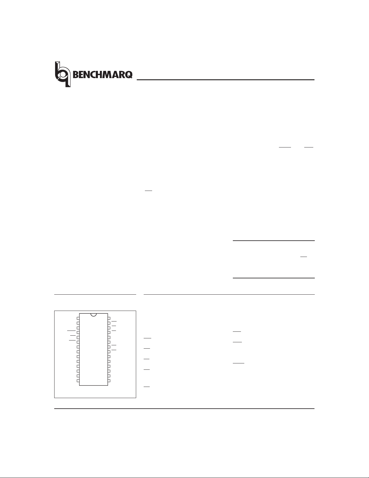
Pin Connections
V
Sept. 1996
OUT
NC
NC
WDO
INT
RST
DQ
DQ
DQ
V
A
3
A
2
A
1
A
0
0
1
2
SS
1
2
3
4
5
6
7
8
9
10
11
12
13
14
28-Pin DIP Module
28
27
26
25
24
23
22
21
20
19
18
17
16
15
PN484701.eps
V
WE
CE
CE
NC
WDI
OE
CS
NC
DQ
DQ
DQ
DQ
DQ
CC
IN
OUT
7
6
5
4
3
Pin Names
A0–A
DQ0–DQ7Data inputs/outputs
WE Write enable
OE
CS Chip select input
CE
IN
CE
OUT
Clock/Control address
3
inputs
Output enable
External RAM chip
enable
Conditional RAM chip
enable
NC No connect
V
OUT
Back-up battery output
INT Interrupt output
RST
Microprocessor reset
WDI Watchdoginput
WDO Watchdogoutput
V
CC
V
SS
+5V supply
Ground
1
bq4847/bq4847Y
Functional Description
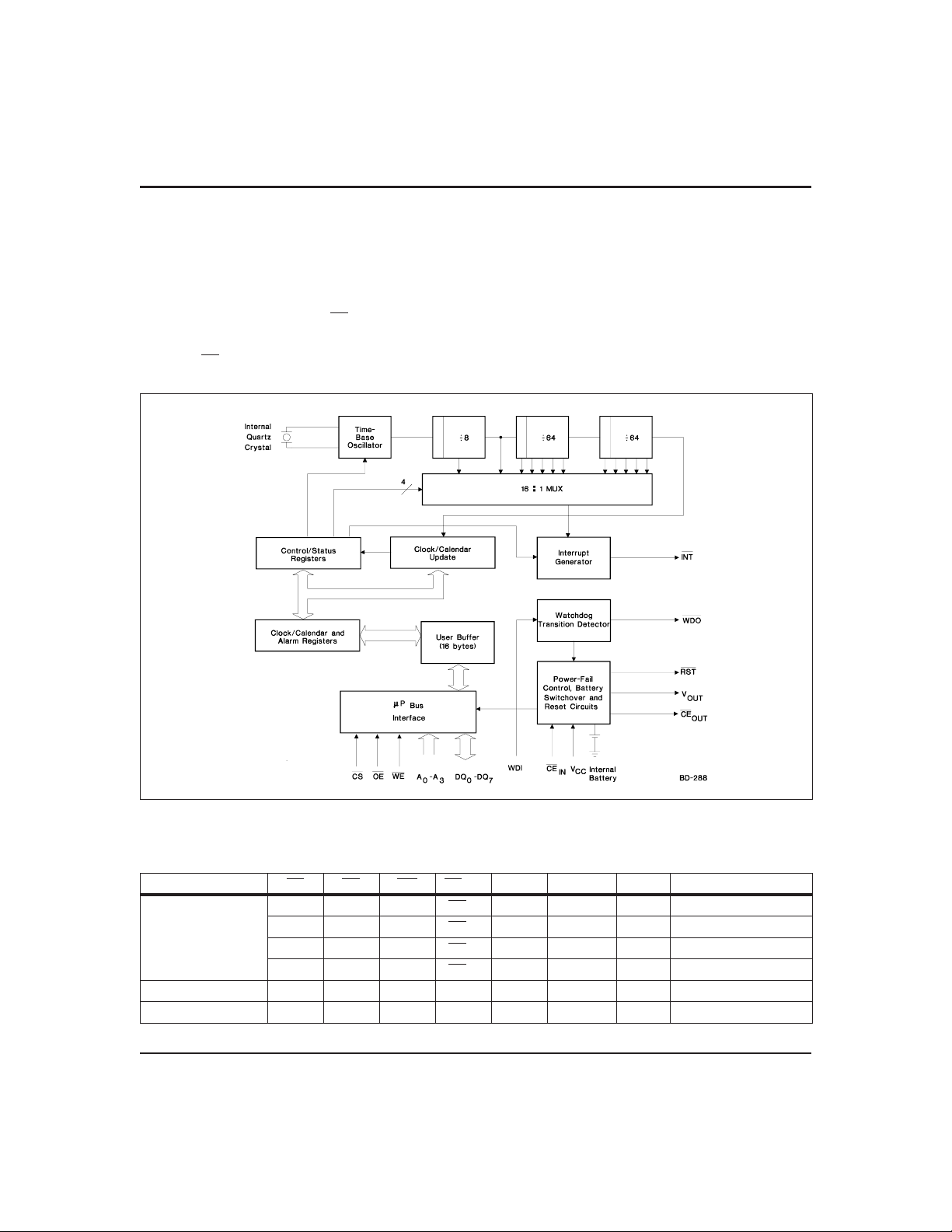
Figure 1 is a block diagram of the bq4847. The bq4847 is
functionally equivalent to the bq4845 except that the battery (20, 24) and crystal (2, 3) pins are not accessible. The
pins are connected internally to a coin cell and quartz
crystal. The coin cell provides 130mAh of capacity. It is internally isolated from V
application of VCC. Once VCCrises above V
tion is broken, and the backup cell provides power to
V
OUT
and CE
for the external SRAM. The real-time
OUT
clock keeps time to within one minute per month at
OUT
and CE
until the initial
OUT
PFD
, this isola-
room temperature. For a complete description of features, operating conditions, electrical characteristics,
bus timing, and pin descriptions, see the bq4845 data
sheet. V alid part types for ordering are bq4847MT (5%)
and bq4847YMT (10%).
Figure 2 illustrates the address map for the bq4847. Table 1 is a map of the bq4847 registers, and Table 2 describes the register bits.
Truth Table
V
CC
(max.) V
<V
CC
(min.) V
>V
CC
(min.) > V
<V
PFD
≤ V
SO
Figure 1. Block Diagram
CS OE WE CE
IH
V
IL
IL
V
IL
XXXVOHV
SO
XXXV
XXCEINV
XVILCE
V
V
V
IL
IH
IH
V
IH
CE
CE
OUT
OHB
V
OUT
OUT1
V
IN
OUT1
V
IN
OUT1
V
IN
OUT1
OUT1
V
OUT2
Mode DQ Power
Deselect High Z Standby
Write D
Read D
IN
OUT
Active
Active
Read High Z Active
Deselect High Z CMOS standby
Deselect High Z Battery-backup mode
Sept. 1996
2

MT: 28-Pin T-Type Module
bq4847/bq4847Y
Ordering Information
bq4847 -MT
28-Pin MT(T-Type Module
Inches Millimeters
Dimension
A 0.360 0.390 9.14 9.91
A1 0.015 - 0.38 -
B 0.015 0.022 0.38 0.56
C 0.008 0.013 0.20 0.33
D 1.520 1.535 38.61 38.99
E 0.710 0.740 18.03 18.80
e 0.590 0.620 14.99 15.75
G 0.090 0.110 2.29 2.79
L 0.110 0.130 2.79 3.30
S 0.100 0.120 2.54 3.05
Min. Max. Min. Max.
)
Sept. 1996
PackageOption:
MT = 28-pin T-type Module
VoltageTolerance:
Blank = 5%
Y = 10%
Device:
bq4847 Real-Time Clock Module WithCPUSupervisor
3

IMPORTANT NOTICE
T exas Instruments and its subsidiaries (TI) reserve the right to make changes to their products or to discontinue
any product or service without notice, and advise customers to obtain the latest version of relevant information
to verify, before placing orders, that information being relied on is current and complete. All products are sold
subject to the terms and conditions of sale supplied at the time of order acknowledgement, including those
pertaining to warranty, patent infringement, and limitation of liability.
TI warrants performance of its semiconductor products to the specifications applicable at the time of sale in
accordance with TI’s standard warranty. Testing and other quality control techniques are utilized to the extent
TI deems necessary to support this warranty . Specific testing of all parameters of each device is not necessarily
performed, except those mandated by government requirements.
CERTAIN APPLICATIONS USING SEMICONDUCTOR PRODUCTS MAY INVOLVE POTENTIAL RISKS OF
DEATH, PERSONAL INJURY, OR SEVERE PROPERTY OR ENVIRONMENTAL DAMAGE (“CRITICAL
APPLICATIONS”). TI SEMICONDUCTOR PRODUCTS ARE NOT DESIGNED, AUTHORIZED, OR
WARRANTED TO BE SUITABLE FOR USE IN LIFE-SUPPORT DEVICES OR SYSTEMS OR OTHER
CRITICAL APPLICA TIONS. INCLUSION OF TI PRODUCTS IN SUCH APPLICATIONS IS UNDERST OOD TO
BE FULLY AT THE CUSTOMER’S RISK.
In order to minimize risks associated with the customer’s applications, adequate design and operating
safeguards must be provided by the customer to minimize inherent or procedural hazards.
TI assumes no liability for applications assistance or customer product design. TI does not warrant or represent
that any license, either express or implied, is granted under any patent right, copyright, mask work right, or other
intellectual property right of TI covering or relating to any combination, machine, or process in which such
semiconductor products or services might be or are used. TI’s publication of information regarding any third
party’s products or services does not constitute TI’s approval, warranty or endorsement thereof.
Copyright 1999, Texas Instruments Incorporated
 Loading...