

www.ti.com
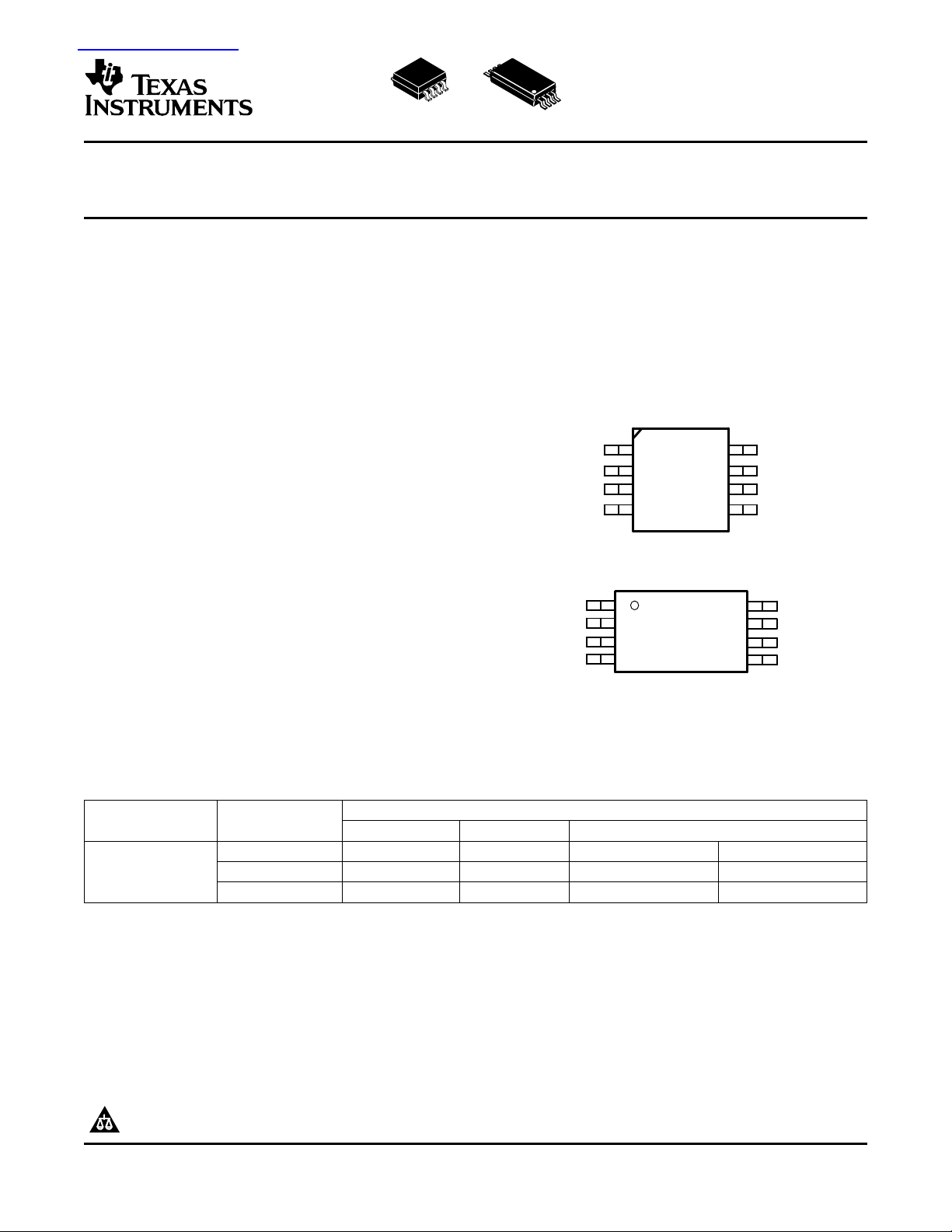
GND
OUT
VDD
CD
VC4
VC1
VC3
1
2 VC2
3
4 5
6
7
8
DCT PACKAGE
(TOP VIEW)
1
2
3
4
8
7
6
5
VC1
VC2
VC3
GND
OUT
VDD
CD
VC4
PW PACKAGE
(TOP VIEW)
查询BQ29410供应商
VOLTAGE PROTECTION FOR 2-, 3-, OR 4-CELL Li-Ion BATTERIES
(2
FEATURES FUNCTION
• 2-, 3-, or 4-Cell Secondary Protection
• Low Power Consumption ICC< 2 µA
[VCELL
• Fixed High Accuracy Overvoltage Protection
Threshold
– bq29410 = 4.35 V
– bq29411 = 4.40 V
– bq29412 = 4.45 V
• Programmable Delay Time of Detection
• High Power Supply Ripple Rejection
• Stable During Pulse Charge Operation
< V
(ALL)
(PROTECT)
]
bq29410, bq29411, bq29412
SLUS669B – AUGUST 2005 – REVISED DECEMBER 2005
nd
-LEVEL PROTECTION)
Each cell in a multiple-cell pack is compared to an
internal reference voltage. If one cell reaches an
overvoltage condition, the protection sequence
begins. The bq2941x device starts charging an
external capacitor through the CD pin. When the CD
pin voltage reaches 1.2 V, the OUT pin changes from
a low level to a high level.
APPLICATIONS
• 2nd-Level Overvoltage Protection in Li-Ion
Battery Packs in:
– Notebook Computers
– Portable Instrumentation
– Portable Equipment
DESCRIPTION
The bq2941x is a secondary overvoltage protection
IC for 2-, 3-, or 4-cell lithium-ion battery packs that
incorporates a high-accuracy precision overvoltage
detection circuit. It includes a programmable delay
circuit for overvoltage detection time.
ORDERING INFORMATION
T
A
–40 ° C to 110 ° C 4.40 V bq29411DCT3R CJH bq29411PW bq29411PWR
(1) For the most current package and ordering information, see the Package Option Addendum at the end of this document, or see the TI
Web site at www.ti.com .
(2) Contact your local Texas Instruments representative or sales office for alternative overvoltage threshold options.
(3) The "R" suffix indicates tape-and-reel packaging.
V
(PROTECT)
(2)
MSOP (DCT3) SYMBOL PW
4.35 V bq29410DCT3R CJG bq29410PW bq29410PWR
4.45 V bq29412DCT3R CJJ bq29412PW bq29412PWR
(1)
PACKAGE
(3)
PRODUCTION DATA information is current as of publication date.
Products conform to specifications per the terms of the Texas
Instruments standard warranty. Production processing does not
necessarily include testing of all parameters.
Please be aware that an important notice concerning availability, standard warranty, and use in critical applications of Texas
Instruments semiconductor products and disclaimers thereto appears at the end of this data sheet.
Copyright © 2005, Texas Instruments Incorporated
www.ti.com
bq29410, bq29411, bq29412
SLUS669B – AUGUST 2005 – REVISED DECEMBER 2005
These devices have limited built-in ESD protection. The leads should be shorted together or the device
placed in conductive foam during storage or handling to prevent electrostatic damage to the MOS gates.
ABSOLUTE MAXIMUM RATINGS
over operating free-air temperature range unless otherwise noted
Supply voltage range VDD –0.3 V to 28 V
Input voltage range
Output voltage range
Continuous total power dissipation See Dissipation Rating Table
Storage temperature range, T
Lead temperature (soldering, 10 s) 300 ° C
(1) Stresses beyond those listed under "absolute maximum ratings" may cause permanent damage to the device. These are stress ratings
only, and functional operation of the device at these or any other conditions beyond those indicated under "recommended operating
conditions" is not implied. Exposure to absolute-maximum-rated conditions for extended periods may affect device reliability.
(2) All voltages are with respect to ground of this device except the differential voltage of VC1-VC2, VC2-VC3, VC3-VC4, and VC4-GND.
VC1, VC2, VC3, VC4 –0.3 V to 28 V
VC1 TO VC2, VC2 TO VC3, VC3 TO VC4, VC4 TO GND –0.3 V to 8 V
OUT –0.3 V to 28 V
CD –0.3 V to 28 V
stg
(1) (2)
UNIT
–65 ° C to 150 ° C
PACKAGE DISSIPATION RATINGS
PACKAGE
DCT 412 mW 3.3 mW/ ° C 264 mW 214 mW
PW 525 mW 4.2 mW/ ° C 336 mW 273 mW
TA= 25 ° C DERATING FACTOR TA= 70 ° C TA= 85 ° C
POWER RATING ABOVE TA= 25 ° C POWER RATING POWER RATING
RECOMMENDED OPERATING CONDITIONS
V
V
t
R
C
R
C
T
Supply voltage 4 25 V
DD
Input voltage range V
I
Delay time capacitance 0.22 µF
d(CD)
Voltage-monitor filter resistance 100 1k Ω
IN
Voltage-monitor filter capacitance 0.01 0.1 µF
IN
Supply-voltage filter resistance 0 1 k Ω
VD
Supply-voltage filter capacitance 0.1 µF
VD
Operating ambient temperature range –40 110 ° C
A
VC1, VC2, VC3, VC4 0 V
VCn – VC (n=1), (n=1, 2, 3), VC4 – GND 0 5
MIN NOM MAX UNIT
DD
2
www.ti.com
bq29410, bq29411, bq29412
SLUS669B – AUGUST 2005 – REVISED DECEMBER 2005
ELECTRICAL CHARACTERISTICS
over recommended operating free-air temperature range, TA= 25 ° C (unless otherwise noted)
PARAMETER TEST CONDITION MIN NOM MAX UNIT
V
(OA)
V
(PROTECT)
V
hys
I
IN
t
D1
I
(CD_dis)
I
CC
I
OH
I
OL
Overvoltage detection
accuracy
Overvoltage
detection voltage
Overvoltage detection
hysteresis
(1)
(1)
Input current 0.3 µA
Overvoltage detection delay
time
CD GND clamp current V
Supply current µA
High-level output current –1 mA
Low-level output current 5 µA
(1) Levels of the overvoltage detection and the hysteresis can be adjusted. For assistance, contact a Texas Instruments sales
representative.
TA= 25 ° C 25 35
TA= –20 ° C to 85 ° C 25 50 mV
TA= –40 ° C to 110 ° C 80
bq29410 4.35
bq29411 4.40 V
bq29412 4.45
V2, V3 , VC4 input ,V
VC1 = VC2 = VC3 = VC4 = 3.5 V (see Figure 1 )
V
= VC1, CD = 0.22 µF 1 1.5 2 S
DD
= VC1, CD = 1 V 5 12 µA
DD
V
= VC1,
DD
VC1–VC2 = VC2–VC3 = VC3–VC4 = VC4–GND = 3.5 V (see 2 3
= VC1
DD
Figure 1 )
V
= VC1,
DD
VC1–VC2 = VC2–VC3 = VC3–VC4 = VC4–GND = 2.3 V (see 1.5 2.5
Figure 1 )
OUT = 3 V, V
VC1–VC2 = VC2–VC3 = VC3–VC4 = VC4–GND = 4.5 V
OUT = 0.1 V, V
VC1–VC2 = VC2–VC3 = VC3–VC4 = VC4–GND = 3.5 V
= VC1,
DD
= VC1,
DD
300 mV
3
www.ti.com
1
2
6
5
8
1
2
6
5
8
1
2
6
5
8
3
4
887
GNDVC4
OUT
VC1
VC2
VC3
VDD
CD
GND
VC4
OUT
VC1
VC2
VC3
VDD
CD
bq29410, bq29411, bq29412
SLUS669B – AUGUST 2005 – REVISED DECEMBER 2005
Figure 1. ICC, IINMeasurement (DCT Package)
Terminal Functions
TERMINAL
MSOP TSSOP
(DCT) (PW)
NAME
8 1 VC1 Sense voltage input for most positive cell
7 2 VC2 Sense voltage input for second most positive cell
6 3 VC3 Sense voltage input for third most positive cell
5 4 GND Ground pin
4 5 VC4 Sense voltage input for least positive cell
3 6 CD An external capacitor is connected to determine the programmable delay time
2 7 VDD Power supply
1 8 OUT Output
DESCRIPTION
4

www.ti.com
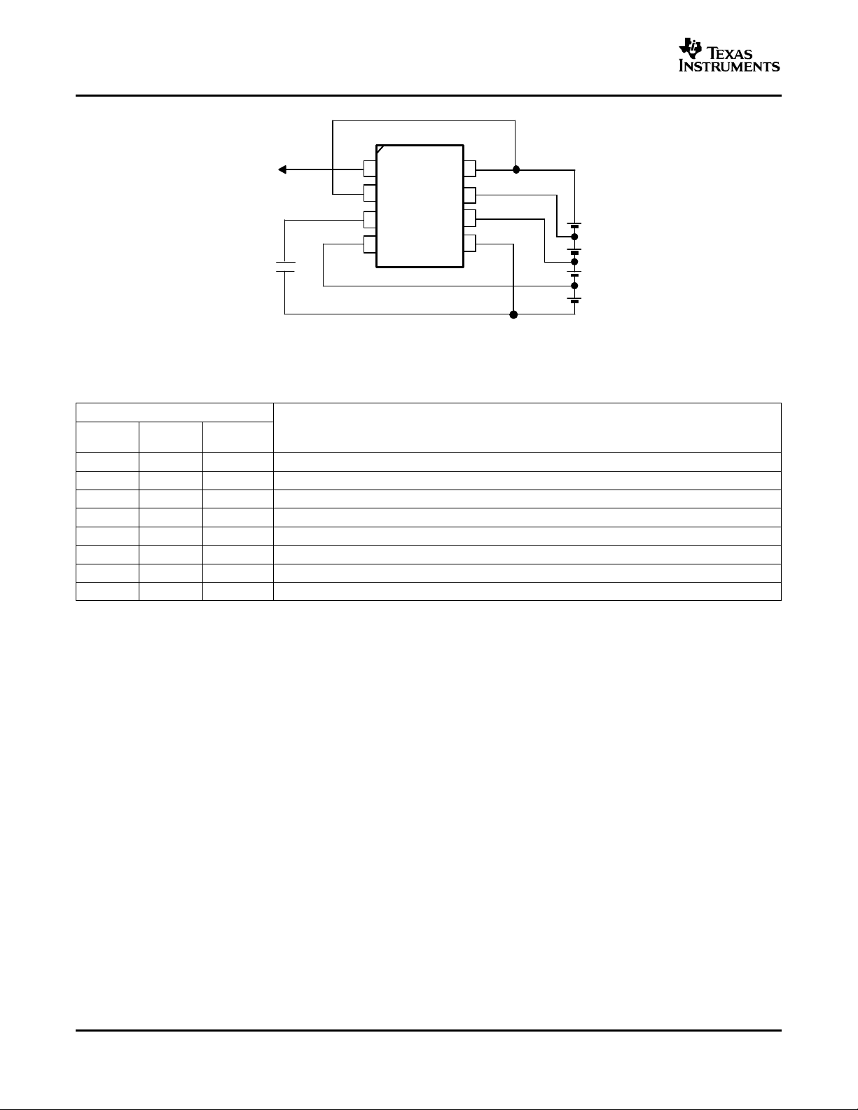
VC1
VC2
VC4
VC3
GND
VDD
OUT
CD
1.2 V (TYP)
R
VD
C
VD
ICD= 0.2 A (TYP)
C
IN
R
IN
R
IN
R
IN
R
IN
C
IN
C
IN
C
IN
C
(DELAY)
t
d
1.2 V C
(DELAY)
I
CD
C
(DELAY)
td I
CD
1.2 V
FUNCTIONAL BLOCK DIAGRAM
bq29410, bq29411, bq29412
SLUS669B – AUGUST 2005 – REVISED DECEMBER 2005
OVERVOLTAGE PROTECTION
When one of the cell voltages exceeds V
C
, connected to the CD pin. If the voltage at the CD pin, V
(DELAY)
(PROTECT)
transitions high. An externally connected NCH FET is activiated and blows the external fuse in the positive
battery rail; see the functional block diagram.
If all cell voltages fall below V
(PROTECT)
before the voltage at pin CD reaches 1.2 V, the delay time does not run
out. An internal switch clamps the CD pin to GND and discharges the capacitor, C
delay time for the next occurring overvoltage event.
Once the pin OUT is activated, it transitions back from high to low after all battery cells reach V
DELAY TIME CALCULATION
The delay time is calculated as follows:
Where I
(CD)
= CD current source = 0.18 µA
, an internal current source begins to charge the capacitor,
reaches 1.2 V, the OUT pin is activated and
CD,
(DELAY)
, and secures the full
(PROTECT)
– V
hys.
5

www.ti.com
V
(PROTECT)
Cell Voltage
(VCn - VC(n-1),
VC4 - GND)
CD
OUT
1.2 V
t
DELAY
V
(PROTECT)
- V
hys
td = (1.2 V x C
DELAY
)/I
CD
224
223
222
111
GNDVC4
OUT
VC1
VC2
VC3
VDD
CD
6
5
8
GNDVC4
OUT
VC1
VC2
VC3
VDD
CD
6
5
8
GNDVC4
OUT
VC1
VC2
VC3
VDD
CD
6
5
8
887
1
2
6
5
8
1
2
6
5
8
1
2
6
5
8
3
4
887
GNDVC4
OUT
VC1
VC2
VC3
VDD
CD
GND
VC4
OUT
VC1
VC2
VC3
VDD
CD
bq29410, bq29411, bq29412
SLUS669B – AUGUST 2005 – REVISED DECEMBER 2005
Figure 2. Timing for Overvoltage Sensing
APPLICATION INFORMATION
BATTERY CONNECTIONS
The following diagrams show the DCT package device in different cell configurations.
Figure 3. 4-Series Cell Configuration Figure 4. 3-Series Cell Configuration
(Connect together VC1 and VC2)
6

www.ti.com
1
2
6
3
4
7
GND
VC4
OUT
VC1
VC2
VC3
VDD
CD
6
5
8
7
SLUS669B – AUGUST 2005 – REVISED DECEMBER 2005
APPLICATION INFORMATION (continued)
Figure 5. 2-Series Cell Configuration
CELL CONNECTIONS
To prevent incorrect output activation, the following connection sequences must be used.
4-Series Cell Configuration
• VC1(=VDD) → VC2 → VC3 → VC4 → GND or
• GND → VC4 → VC3 → VC2 → VC1(=VDD)
3-Series Cell Configuration
• VC1(=VC2=VDD) → VC3 → VC4 → GND or
• GND → VC4 → VC3 → VC1(=VC2=VDD)
2-Series Cell Configuration
• VC1(=VC2=VC3=VDD) → VC4 → GND or
• GND → VC4 → VC1(=VC2=VC3=VDD)
bq29410, bq29411, bq29412
7

PACKAGE OPTION ADDENDUM
www.ti.com
12-Dec-2005
PACKAGING INFORMATION
Orderable Device Status
(1)
Package
Type
Package
Drawing
Pins Package
Qty
Eco Plan
BQ29412DCT3R ACTIVE SM8 DCT 8 3000 Pb-Free
(1)
The marketing status values are defined as follows:
ACTIVE: Product device recommended for new designs.
LIFEBUY: TI has announced that the device will be discontinued, and a lifetime-buy period is in effect.
NRND: Not recommended for new designs. Device is in production to support existing customers, but TI does not recommend using this part in
a new design.
PREVIEW: Device has been announced but is not in production. Samples may or may not be available.
OBSOLETE: TI has discontinued the production of the device.
(2)
Eco Plan - The planned eco-friendly classification: Pb-Free (RoHS) or Green (RoHS & no Sb/Br) - please check
http://www.ti.com/productcontent for the latest availability information and additional product content details.
TBD: The Pb-Free/Green conversion plan has not been defined.
Pb-Free (RoHS): TI's terms "Lead-Free" or "Pb-Free" mean semiconductor products that are compatible with the current RoHS requirements
for all 6 substances, including the requirement that lead not exceed 0.1% by weight in homogeneous materials. Where designed to be soldered
at high temperatures, TI Pb-Free products are suitable for use in specified lead-free processes.
Green (RoHS & no Sb/Br): TI defines "Green" to mean Pb-Free (RoHS compatible), and free of Bromine (Br) and Antimony (Sb) based flame
retardants (Br or Sb do not exceed 0.1% by weight in homogeneous material)
(3)
MSL, Peak Temp. -- The Moisture Sensitivity Level rating according to the JEDEC industry standard classifications, and peak solder
temperature.
(RoHS)
(2)
Lead/Ball Finish MSL Peak Temp
CU SNBI Level-1-250C-UNLIM
(3)
Important Information and Disclaimer:The information provided on this page represents TI's knowledge and belief as of the date that it is
provided. TI bases its knowledge and belief on information provided by third parties, and makes no representation or warranty as to the
accuracy of such information. Efforts are underway to better integrate information from third parties. TI has taken and continues to take
reasonable steps to provide representative and accurate information but may not have conducted destructive testing or chemical analysis on
incoming materials and chemicals. TI and TI suppliers consider certain information to be proprietary, and thus CAS numbers and other limited
information may not be available for release.
In no event shall TI's liability arising out of such information exceed the total purchase price of the TI part(s) at issue in this document sold by TI
to Customer on an annual basis.
Addendum-Page 1

MECHANICAL DATA
MPDS049B – MA Y 1999 – REVISED OCT OBER 2002
DCT (R-PDSO-G8) PLASTIC SMALL-OUTLINE PACKAGE
0,65
PIN 1
INDEX AREA
0,30
0,15
8
1
3,15
2,75
5
2,90
2,70
4
1,30 MAX
M
0,13
4,25
3,75
Seating Plane
0,15 NOM
0° – 8°
Gage Plane
0,25
0,60
0,20
0,10
0,00
NOTES: A. All linear dimensions are in millimeters.
B. This drawing is subject to change without notice.
C. Body dimensions do not include mold flash or protrusion
D. Falls within JEDEC MO-187 variation DA.
0,10
4188781/C 09/02
POST OFFICE BOX 655303 • DALLAS, TEXAS 75265

IMPORTANT NOTICE
Texas Instruments Incorporated and its subsidiaries (TI) reserve the right to make corrections, modifications,
enhancements, improvements, and other changes to its products and services at any time and to discontinue
any product or service without notice. Customers should obtain the latest relevant information before placing
orders and should verify that such information is current and complete. All products are sold subject to TI’s terms
and conditions of sale supplied at the time of order acknowledgment.
TI warrants performance of its hardware products to the specifications applicable at the time of sale in
accordance with TI’s standard warranty. Testing and other quality control techniques are used to the extent TI
deems necessary to support this warranty . Except where mandated by government requirements, testing of all
parameters of each product is not necessarily performed.
TI assumes no liability for applications assistance or customer product design. Customers are responsible for
their products and applications using TI components. To minimize the risks associated with customer products
and applications, customers should provide adequate design and operating safeguards.
TI does not warrant or represent that any license, either express or implied, is granted under any TI patent right,
copyright, mask work right, or other TI intellectual property right relating to any combination, machine, or process
in which TI products or services are used. Information published by TI regarding third-party products or services
does not constitute a license from TI to use such products or services or a warranty or endorsement thereof.
Use of such information may require a license from a third party under the patents or other intellectual property
of the third party, or a license from TI under the patents or other intellectual property of TI.
Reproduction of information in TI data books or data sheets is permissible only if reproduction is without
alteration and is accompanied by all associated warranties, conditions, limitations, and notices. Reproduction
of this information with alteration is an unfair and deceptive business practice. TI is not responsible or liable for
such altered documentation.
Resale of TI products or services with statements different from or beyond the parameters stated by TI for that
product or service voids all express and any implied warranties for the associated TI product or service and
is an unfair and deceptive business practice. TI is not responsible or liable for any such statements.
Following are URLs where you can obtain information on other Texas Instruments products and application
solutions:
Products Applications
Amplifiers amplifier.ti.com Audio www.ti.com/audio
Data Converters dataconverter.ti.com Automotive www.ti.com/automotive
DSP dsp.ti.com Broadband www.ti.com/broadband
Interface interface.ti.com Digital Control www.ti.com/digitalcontrol
Logic logic.ti.com Military www.ti.com/military
Power Mgmt power.ti.com Optical Networking www.ti.com/opticalnetwork
Microcontrollers microcontroller.ti.com Security www.ti.com/security
Telephony www.ti.com/telephony
Video & Imaging www.ti.com/video
Wireless www.ti.com/wireless
Mailing Address: Texas Instruments
Post Office Box 655303 Dallas, Texas 75265
Copyright 2005, Texas Instruments Incorporated

Copyright © Each Manufacturing Company.
All Datasheets cannot be modified without permission.
This datasheet has been download from :
www.AllDataSheet.com
100% Free DataSheet Search Site.
Free Download.
No Register.
Fast Search System.
www.AllDataSheet.com
 Loading...