

VBUS
VBUS
GND
HOST
bq24180
SW
PSEL
SCL
DCOUT
C1
1 µF
C2
10µF
C3
4.7µF
R3
4 kW
SYSTEM
PMID
SDA
D+
D-
USBPHY
BOOT
PGND
CSIN
CSOUT
VAUX
STAT
POWERFOR
ACCESSORY
C4
10nF
C 6
1 µF
C 5
0.1µF
RSNS
68 mW
R1
10kW
R2
VBUS
TS
TEMP
PACK+
PACK-
DRV
C7
1 µF
VBUS
INT
R4
C 8
1 µF
CD
HardwareDisable
10kW 10kW
bq24180
www.ti.com
SLUSA02 A –FEBRUARY 2010–REVISED FEBRUARY 2010
Fully Integrated Switch-Mode One-Cell Li-Ion Charger with Full USB Compliance and
Accessory Power Connection
Check for Samples: bq24180
1
FEATURES
2
• Charge Faster than Linear Chargers From
Current Limited Input Sources • Programmable Charge Parameters through
• High-Accuracy Voltage and Current Regulation
– Input Current Regulation Accuracy: ±5%
(100mA, 500mA)
– Charge Voltage Regulation Accuracy:
±0.5% (25°C), ±1% (0–125°C)
– Charge Current Regulation Accuracy: ±5%
• Accessory Power Output (DCOUT)
• Input Voltage Based Dynamic Power
Management
• Safety Limit Register for Maximum Charge
Voltage and Current Limiting
• High-Efficiency Mini-USB/AC Battery Charger
for Single-Cell Li-Ion and Li-Polymer Battery
Packs
• 20-V Absolute Maximum and 16.5V Operation
Input Voltage Rating
• Built-in Input Current Sensing and Limiting
• Integrated Power FETs for Up to 1.5-A Charge
Rate
I2C™ compatible Interface (up to 3.4 Mbps)
• Synchronous Fixed-Frequency PWM
Controller Operating at 3 MHz With 0% to
99.5% Duty Cycle
• Safety Timer and Software Watchdog
• Reverse Leakage Protection Prevents Battery
Drainage
• Thermal Regulation and Protection
• Status Outputs for Charging and Faults
• 25-Pin WCSP Package
APPLICATIONS
• Mobile Phones and Smart Phones
• Portable Media Players
• Handheld Devices
DESCRIPTION
The bq24180 is a compact, flexible, high-efficiency, USB-friendly switch-mode charge management device for
single-cell Li-ion and Li-polymer batteries used in a wide range of portable applications. The charge parameters
is programmable using an I2C compatible interface. The bq24180 integrates a synchronous PWM controller,
power MOSFETs, input current sensing and overvoltage protection, high-accuracy current and voltage regulation,
and charge termination, into a small WCSP package.
1
2
2I
C is a trademark of Phillips Electronics.
PRODUCTION DATA information is current as of publication date.
Products conform to specifications per the terms of the Texas
Instruments standard warranty. Production processing does not
necessarily include testing of all parameters.
Please be aware that an important notice concerning availability, standard warranty, and use in critical applications of Texas
Instruments semiconductor products and disclaimers thereto appears at the end of this data sheet.
Copyright © 2010, Texas Instruments Incorporated
bq24180
SLUSA02 A –FEBRUARY 2010–REVISED FEBRUARY 2010
This integrated circuit can be damaged by ESD. Texas Instruments recommends that all integrated circuits be handled with
appropriate precautions. Failure to observe proper handling and installation procedures can cause damage.
ESD damage can range from subtle performance degradation to complete device failure. Precision integrated circuits may be more
susceptible to damage because very small parametric changes could cause the device not to meet its published specifications.
www.ti.com
DESCRIPTION (CONTINUED)
The bq24180 charges the battery in three phases: conditioning, constant current and constant voltage. Charge
current is programmable using the I2C interface. Additionally, the input current can be limited to a host
programmable threshold to maintain maximum charge current from current-limited sources, such as USB ports.
Charge is terminated based on user-selectable minimum current level. A software watchdog provides a safety
backup for I2C interface while a safety timer prevents overcharging the battery. During normal operation,
bq24180 automatically restarts the charge cycle if the battery voltage falls below an internal threshold and
automatically enters sleep mode or high impedance mode when the input supply is removed. The charge status
is reported to the host using the I2C interface. During the charging process, the bq24180 monitors its junction
temperature (TJ) and reduces the charge current if TJincreases to 125°C. The bq24180 is available in 25-pin
WCSP package.
ORDERING INFORMATION
PART NUMBER
bq24180YFFR 16.5 V 6B
bq24180YFFT 16.5 V 6B
(1) The YFF package is available in the following options:
R – taped and reeled in quantities of 3,000 devices per reel.
T – taped and reeled in quantities of 250 devices per reel.
(2) This product is RoHS compatible, including a lead concentration that does not exceed 0.1% of total product weight, and is suitable for
use in specified lead-free soldering processes. In addition, this product uses package materials that do not contain halogens, including
bromine (Br) or antimony (Sb) above 0.1% of total product weight.
(1)(2)
V
OVP
I2C ADDRESS
ABSOLUTE MAXIMUM RATINGS
(1)(2)
over operating free-air temperature range (unless otherwise noted)
LIMITS UNIT
Supply voltage range (with respect to PGND) VBUS –2 to 20 V
Input voltage range (with respect to and PGND) SCL, SDA, PSEL, CSIN, CSOUT, DRV, DCOUT, INT –0.3 to 7 V
Output voltage range (with respect to and PGND) V
Voltage difference between CSIN and CSOUT inputs (VCSIN –VCSOUT) ±7 V
Voltage difference between BOOT and SW inputs (VBOOT –VSW) –0.3 to 7 V
Output sink mA
Output current DCOUT 1.5 A
Output current (average) SW 2 A
T
A
T
J
T
stg
(1) Stresses beyond those listed under absolute maximum ratings may cause permanent damage to the device. These are stress ratings
only, and functional operation of the device at these or any other conditions beyond those indicated under recommended operating
conditions is not implied. Exposure to absolute-maximum-rated conditions for extended periods may affect device reliability.
(2) All voltages are with respect to GND if not specified. Currents are positive into, negative out of the specified terminal. Consult Packaging
Section of the data book for thermal limitations and considerations of packages.
Operating free-air temperature range –30 to +85 °C
Junction temperature range –40 to +125 °C
Storage temperature –45 to +150 °C
PMID, STAT –0.3 to 20
SW, BOOT –0.7 to 20
INT 5
STAT 10
DRV 10 mA
2 Submit Documentation Feedback Copyright © 2010, Texas Instruments Incorporated
Product Folder Link(s): bq24180
bq24180
www.ti.com
SLUSA02 A –FEBRUARY 2010–REVISED FEBRUARY 2010
DISSIPATION RATINGS
PACKAGE R
WCSP-25 60°C/W
(1) Using JEDEC 2s2p PCB standard.
qJA
R
qJC
(1)
1.57°C/W 540 mW 5.4 mW/°C
TA< 25°C DERATING FACTOR
POWER RATING ABOVE TA= 25°C
RECOMMENDED OPERATING CONDITIONS
over operating free-air temperature range (unless otherwise noted)
MIN NOM MAX UNIT
Supply voltage, VBUS 4.0 16
Operating junction temperature range, T
J
0 125 °C
(1) The inherent switching noise voltage spikes should not exceed the absolute maximum rating on either the BOOT or SW pins. A tight
layout minimizes switching noise.
(1)
ELECTRICAL CHARACTERISTICS
Circuit of Figure 2, V
noted)
INPUT CURRENTS
I
VBUS
I
VBUS_LEAK
I
BAT_DCOUT
I
BAT_HIZ
VOLTAGE REGULATION
V
OREG
CURRENT REGULATION - FAST CHARGE
I
OCHARGE
PSEL, CD LOGIC LEVEL
V
IL
V
IH
CHARGE TERMINATION DETECTION
I
TERM
I
TERM_dgl
INPUT BASED DYNAMIC POWER MANAGEMENT
V
VBUS
Leakage current from battery to VBUS pin 0°C< TJ< 85°C, V
Battery Current when using DCOUT 800 µA
Battery discharge current in High Impedance
mode, (CSIN, CSOUT, SW pins)
Output charge voltage programmable range Operating in voltage regulation, programmable 3.5 4.44 V
Voltage regulation accuracy
Output charge current programmable range 550 1550 mA
Regulation accuracy for charge current V
across RSNS
V
IREG
Input low threshold level PSEL, CD falling 0.4 V
Input high threshold level PSEL, CD rising 1.2 V
Termination charge current 25 200 mA
Deglitch time for charge termination 30 ms
Regulation accuracy for termination current
across R
V
IREG_TERM
Battery Detection sink current before charge
done
= 5V, HZ_MODE=0, CD=0, TJ= –40°C to 125°C and TJ= 25°C for typical values (unless otherwise
VBUS
PARAMETER TEST CONDITIONS MIN TYP MAX UNIT
V
supply current for control V
VBUS
VBUS
> V
> V
, PWM switching 10 mA
VBUS(min)
, PWM NOT switching 5 mA
VBUS(min)
0°C< TJ< 85°C, EN=0 or HZ_MODE=1 650 µA
= 4.2 V, No input connected 5 µA
CSOUT
DCOUT = enabled, V
I
=750mA
DCOUT
0°C< TJ< 85°C, V
DCOUT disabled SCL,SDA=0V or 1.8V
= 4.2V, DCOUT_ILIM=1A,
BAT
= 4.2 V, No Input connected,
CSOUT
30 µA
0°C< TJ < 85°C, VCSOUT = 4.2 V, High Impedance
mode, DCOUT disabled, V
SCL,SDA=0V or 1.8V
= 5V, 60 µA
VBUS
TA= 25°C –0.5% 0.5%
–1% 1%
V
= I
OCHARGE
× R
SNS
≤ V
PRECHG
R
= 68 mΩ, Programmable
SNS
= 37.4 mV to 44.2 mV –3.5% 3.5%
ICHRG
V
> 44.2 mV –3.0% 3.0%
ICHRG
V
> V
CSOUT
R
= 68 MΩ, Programmable
SNS
< V
CSOUT
OREG–VRCH
OREG
, V
VBUS>VSLP
, V
VBUS>VSLP
,
,
Both rising and falling, 2-mV over- drive,
t
, t
= 100 ns
FALL
= 1.7 mV –40% 40%
TERM
= 3.4 mV to 6.8 mV –16% 16%
TERM
= 6.8 mV to 13.6 mV –11% 11%
TERM
≥ 13.6 mV –5.5% 5.5%
TERM
SNS
= I
OTERM
× R
SNS
RISE
V
V
V
V
–550 µA
V
Copyright © 2010, Texas Instruments Incorporated Submit Documentation Feedback 3
Product Folder Link(s): bq24180
bq24180
SLUSA02 A –FEBRUARY 2010–REVISED FEBRUARY 2010
ELECTRICAL CHARACTERISTICS (continued)
Circuit of Figure 2, V
noted)
V
IN_DPM
FAULTY ADAPTER PROTECTION
V
VBUS (MIN)
t
INT
INPUT CURRENT LIMITING
I
IN_LIMIT
DCOUT
R
DCOUT
I
LIM_DCOUT
t
DGL_DCOUT
I
LIM_DCOUT
BATTERY RECHARGE THRESHOLD
V
RCH
STAT OUTPUTS
V
OL(STAT)
V
OL(INT)
I2C BUS LOGIC LEVELS AND TIMING CHARACTERISTICS
V
OL
I
(bias)
f
SCL
SLEEP COMPARATOR
V
SLP
V
SLP-EXIT
UVLO
V
UVLO
V
UVLO_HYS
PWM
The threshold when input based DPM loop
kicks in
DPM loop kick-in threshold tolerance –2% 2%
Faulty adapter threshold 3.6 3.8 4.0 V
Deglitch time for Faulty adapter 30 ms
Hysteresis for faulty adapter protection V
Current source for faulty adapter protection 20 30 40 mA
Detection Interval 2 s
Input current limiting threshold I
DCOUT Pass FET on-resistance I
DCOUT current limit programmable range 350 1400 mA
Deglitch time from DCOUT current-limit event
to DCOUT latch-off
DCOUT current limit range mA
Recharge threshold voltage Below VOREG 100 120 150 mV
Deglitch time 130 ms
Low-level output saturation voltage, STAT IO= 10 mA, sink current 0.5 V
High-level leakage current Voltage on STAT pin is 5V 1 µA
Low-level output saturation voltage, INT IO= 1 mA, sink current 0.4 V
High-level leakage current Voltage on INT pin is 5V 1 µA
Output low threshold level IO= 10 mA, sink current 0.4 V
Input low threshold level V
Input high threshold level V
Input bias current V
SCL clock frequency 3.4 MHz
Sleep-mode entry threshold,
V
BUS-VCSOUT
Sleep-mode exit hysteresis 2.3 V ≤ V
Deglitch time for VBUS rising above
V
SLP+VSLP_EXIT
IC active threshold voltage V
IC active hysteresis V
Internal top reverse blocking MOSFET
on-resistance
Internal top N-channel Switching MOSFET
on-resistance
= 5V, HZ_MODE=0, CD=0, TJ= –40°C to 125°C and TJ= 25°C for typical values (unless otherwise
VBUS
PARAMETER TEST CONDITIONS MIN TYP MAX UNIT
Charge mode, programmable 4.15 4.71 V
Rising 100 200 mV
VBUS
USB charge mode, current
pulled from PMID
= 500 mA 300 mΩ
DCOUT
Programmable via I2C
Programmable via I2C
V
decreasing below threshold,
CSOUT
t
= 100 ns, 10-mV overdrive
FALL
= 1.8 V, SDA and SCL 0.4 V
(pull-up)
= 1.8 V, SDA and SCL 1.2 V
(pull-up)
= 1.8 V, SDA and SCL 1 µA
(pull-up)
2.3 V ≤ V
CSOUT
CSOUT
Rising voltage, 2-mV over drive, t
rising 3.05 3.3 3.55 V
VBUS
falling from above V
VBUS
I
= 500 mA, Measured from V
IN_LIMIT
Measured from PMID to SW 130 250 mΩ
≤ V
< V
OREG
OREG
I
= 100 mA 90 95 100
IN_LIMIT
= 500 mA 450 475 500 mA
IN_LIMIT
I
= 800 mA 700 755 800
IN_LIMIT
14.5 ms
I
LIM_DCOUT
I
LIM_DCOUT
I
LIM_DCOUT
I
LIM_DCOUT
, V
falling 0 40 100 mV
VBUS
= 350mA 270 350
= 750mA 650 750
= 1050mA 800 1050
= 1400mA 1050 1400
140 200 260 mV
= 100 ns 30 ms
RISE
UVLO
to PMID 110 210 mΩ
VBUS
120 150 mV
www.ti.com
4 Submit Documentation Feedback Copyright © 2010, Texas Instruments Incorporated
Product Folder Link(s): bq24180
bq24180
www.ti.com
SLUSA02 A –FEBRUARY 2010–REVISED FEBRUARY 2010
ELECTRICAL CHARACTERISTICS (continued)
Circuit of Figure 2, V
noted)
Internal bottom N-channel MOSFET
on-resistance
f
OSC
D
MAX
D
MIN
V
DRV
I
DRV
V
DO_DRV
PROTECTION
V
OVP
V
IN_HIGH
t
OVP-dgl
I
LIMIT
V
PRECHG
I
PRECHG
T
SHTDWN
T
CF
t
WATCHDOG
V
HOT
V
WARM
V
COLD
I
TS
(1) Bottom N-channel MOSFET always turns on for ~60 ns and then turns off if current is too low.
Oscillator frequency 3.0 MHz
Frequency accuracy –10% 10%
Maximum duty cycle 99.5%
Minimum duty cycle 0
Synchronous mode to non-synchronous
mode transition current threshold
Internal bias voltage regulator I
DRV Output Current External load on DRV 10 mA
DRV Dropout Voltage (V
Input OVP threshold voltage Threshold over V
V
hysteresis V
OVP
Input High threshold V
VIN_HIGH_USB hysteresis V
OVP deglitch time V
Cycle-by-cycle current limit for charge Charge mode operation 1.8 2.4 3.0 A
Precharge to fast charge threshold V
VPRECHG hysteresis V
Precharge charge charging current V
Thermal trip 165 °C
Thermal hysteresis 10 °C
Thermal regulation threshold Charge current begins to taper down 120 °C
Timeout for the watchdog timer Watchdog timer 12 s
Safety timer accuracy –20% 20%
TS Hot Threshold Corresponds to 55°C, VTSFalling 0.153 0.160 0.169 V
TS Hot Threshold Hysteresis VTS Rising 12.5 mV
TS Warm Threshold Corresponds to 45°C VTSFalling 0.210 0.225 0.240 V
TS Warm Threshold Hysteresis VTSRising 12.5 mV
TS Cold Threshold Corresponds to 5°C, VTSRising 1.06 1.10 1.14 V
TS Cold Threshold Hysteresis VTSFalling 75 mV
TS Bias Current 95 100 105 µA
TS Open Resistance Resistance on TS that translates to open circuit on TS 200 kΩ
= 5V, HZ_MODE=0, CD=0, TJ= –40°C to 125°C and TJ= 25°C for typical values (unless otherwise
VBUS
PARAMETER TEST CONDITIONS MIN TYP MAX UNIT
Measured from SW to PGND 125 210 mΩ
Low-side MOSFET cycle-by-cycle current sensing 100 mA
= 10 mA 5 5.2 5.45 V
DRV
I
= 1A, V
VBUS
V
< V
UVLO
falling from above V
VBUS
Rising, Threshold where I
VBUS
falling from above V
VBUS
rising or falling 32 ms
VBUS
rising 1.9 2.0 2.1 V
CSOUT
falling from above V
CSOUT
≤ V
CSOUT
VBUS
VBUS<VSLP
VBUS
and V
SHORT
= 5 V, I
= 10 mA 340
DRV
to turn off converter during charge 16 16.5 17 V
OVP
falls to 50 mA 9.5 9.8 10.1 V
BAT
IN_HIGH
PRECHG
< V
IN_HIGH
VBUS
< V
OVP
VBUS
(1)
– V
) mV
DRV
750
185 mV
150 mV
100 mV
33.5 50.0 66.5 mA
Copyright © 2010, Texas Instruments Incorporated Submit Documentation Feedback 5
Product Folder Link(s): bq24180
VBUS
SW
+
+
BOOT
DRV
VDRV
CSIN
CSOUT
V
PRECHG
+ -
+
InputCurrentLimit
Amplifier
INT
+
+
+
REF
TS
TSHOT
TSWARM
TSCOLD
DISABLE
V
PRECHG
Comparator
+
V
BATREG
Amplifier
PMID
DC-DC
CONVERTER
PWMLOGIC
AND
COMPENSATION
400mA
maxcharge
V
OREG
I
IN_LIMIT
Gm
amp
I
OUTREG
Amplifier
Charge
Pump
+
Sleep
Comparator
V
BAT
V
IN
5.2V
Reference
+
Recharge
Comparator
Termination
Comparator
I2Cand
CHARGE
CONTROLLER
PGND
PSEL
SDA
SCL
DCOUT
+
V
IN
50mA Precharge
CurrentSource
-
+
130mV
V
ICHRG
V
ITERM
VDRV
Charge
Pump
+
16.5V
OVP
Comparator
High-Input
Comparator
9.8V
+
VIN-DPM
Amplifier
V
INDPM
V
HIGH
Comparator
+
DCOUT _ILIM
TMR
SAFETY
TIMERS
2X
TIMER
FAULT
Q1
Q2
Q3
Q4
Q5
REF
100uA
+
+
ThermalReg
Amplifier
125°C
T
J
STAT
CD
bq24180
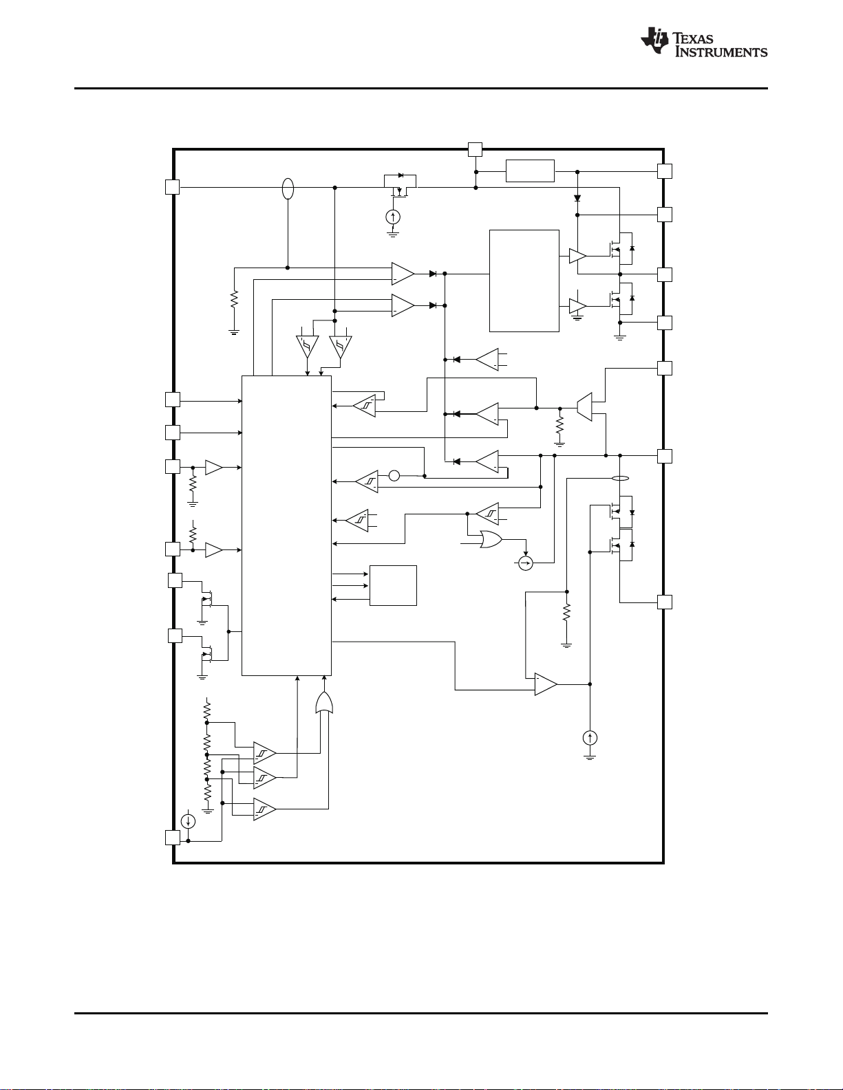
SLUSA02 A –FEBRUARY 2010–REVISED FEBRUARY 2010
SIMPLIFIED BLOCK DIAGRAM
www.ti.com
6 Submit Documentation Feedback Copyright © 2010, Texas Instruments Incorporated
Figure 1. Simplified Block Diagram
Product Folder Link(s): bq24180
VBUS VBUS BOOT SCL
PMID PMID PMID CD
SW SW SW PSEL
PGND PGND PGND
STAT
DRV
DCOUT
CSIN CSOUT
SDA
INT
DCOUT
CSOUTTS
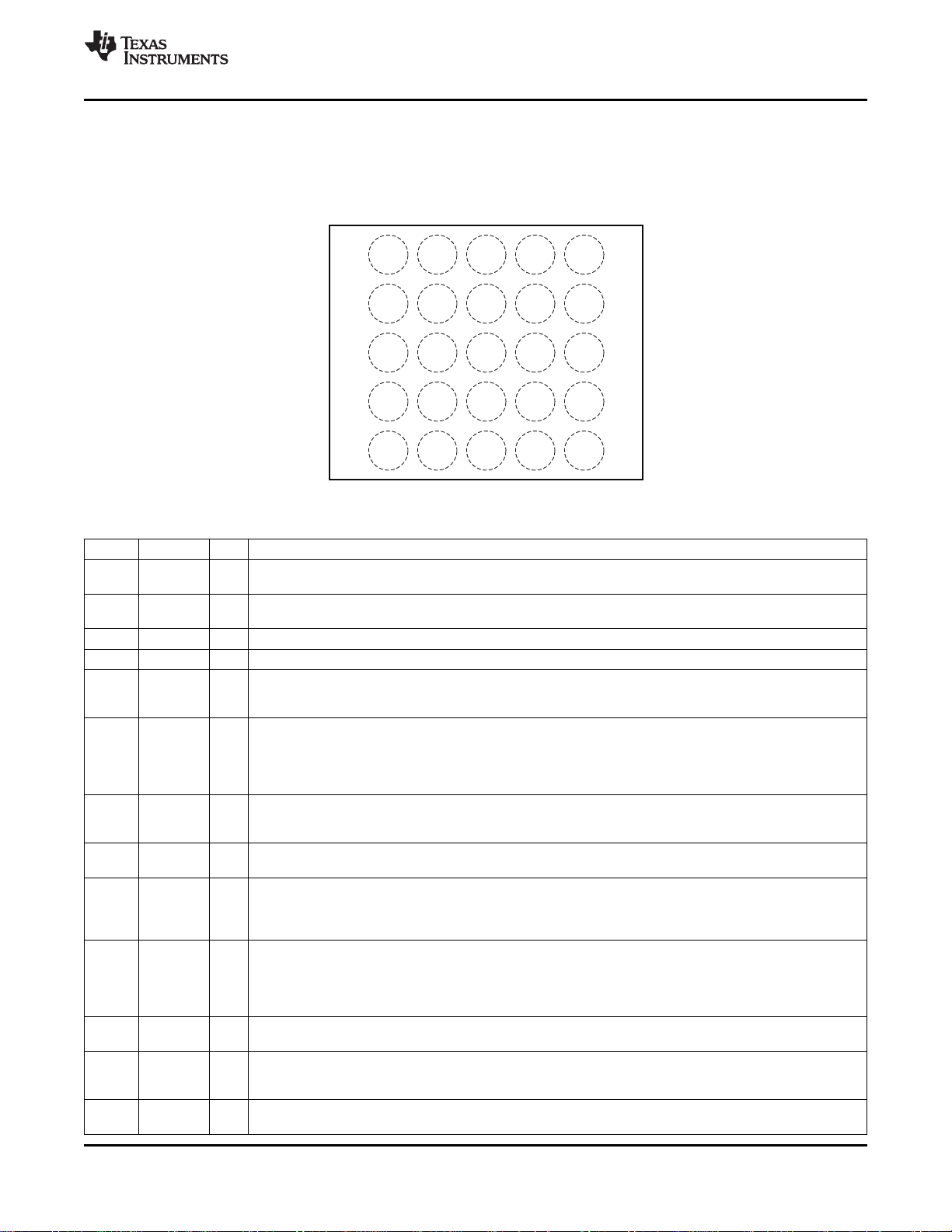
1 2 3 4 5
A
B
C
D
E
2.2mmx2.4mm25-pinWCSP
TOP VIEW
bq24180
www.ti.com
SLUSA02 A –FEBRUARY 2010–REVISED FEBRUARY 2010
DEVICE INFORMATION
PIN CONFIGURATION
PIN FUNCTIONS
NAME PIN NO. I/O DESCRIPTION
VBUS A1, A2 I/O Charger Input Voltage. Connect to an input supply up to 16V. Bypass VBUS to PGND with a 1µF ceramic
BOOT A3 O High-Side MOSFET Gate Driver Supply. Connect a 10nF ceramic capacitor (voltage rating above 10V) from
SCL A4 I I2C interface clock. Connect SCL to the logic rail through a 10kΩ resistor.
SDA A5 I/O I2C interface data. Connect SCL to the logic rail through a 10kΩ resistor.
PMID B1, B2, B3 O Connection Point Between Reverse Blocking MOSFET and High-Side Switching MOSFET. Bypass PMID to
INT B4 O Host Interface Status Output. INT is a low voltage open drain output used to signal charge status to the host
CD B5 O Hardware Disable Input. Connect CD to GND to enable charge. Drive CD high to disable charge and place
SW C1, C2, O Inductor Connection. Connect the switched side of the inductor to SW.
C3
PSEL C4 I USB Source Detection Input. Drive PSEL high to indicate a USB source is connected to the input and the PC
STAT C5 O Status Output. STAT is an open drain output that is pulled low during charging. When charging is complete or
PGND D1, D2, Power ground. Connect to the ground plane for the circuit.
D3
DCOUT D4, D5 O Accessory Power Output. DCOUT is connected to the battery through an internal pass FET. When enabled
CSIN E1 I Charge Current-Sense Input. Battery current is sensed via the voltage drop across an external sense resistor.
Copyright © 2010, Texas Instruments Incorporated Submit Documentation Feedback 7
capacitor.
BOOT pin to SW pin to supply the gate drive for the high side MOSFET.
PGND with a minimum of 3.3µF ceramic capacitor. Use caution when connecting an external load to PMID.
The PMID output is not current limited. Any short on PMID will result in damage to the IC.
processor. INT is pulled low during charging. When charging is complete or when charging is disabled, INT is
high impedance. When a fault occurs, a 128µs pulse is sent out as an interrupt for the host. INT is
enabled/disabled using the EN_STAT bit in the control register. Connect INT to a logic rail through a 10kΩ
resistor to communicate with the host processor.
the bq24180 into high impedance mode. Toggling CD resets the safety timer when in DEFAULT mode, but
does not reset the timer when in host mode. CD is pulled to PGND through a 100kΩ internal resistor.
mode default values should be used. When PSEL is high, the IC starts up with a 100mA input current limit.
Drive PSEL low to indicate that an AC Adapter is connected to the input. When PSEL is low, the IC starts up
with no input current limit and a 1A charge current. PSEL has an internal 100kΩ pullup resistor.
when charging is disabled, STAT is high impedance. When a fault occurs, a 128µs pulse is sent out as an
interrupt for the host. STAT is enabled/disabled using the EN_STAT bit in the control register. Connect STAT
to a logic rail using an LED for visual indication or through a 10kΩ resistor to communicate with the host
processor.
through I2C, DCOUT is connected to the battery. When disabled, DCOUT is high-impedance. Bypass DCOUT
to PGND with at least a 1µF ceramic capacitor.
Bypass CSIN to PGND with a 0.1µF ceramic capacitor.
Product Folder Link(s): bq24180
bq24180
SLUSA02 A –FEBRUARY 2010–REVISED FEBRUARY 2010
www.ti.com
PIN FUNCTIONS (continued)
NAME PIN NO. I/O DESCRIPTION
TS E2 I Battery Pack NTC Monitor. Connect TS to a 4.7kΩ NTC thermistor. During DEFAULT mode, when VTS>
DRV E3 O Gate Drive Supply. DRV is the supply for the gate drive of the internal MOSFETs. Bypass DRV to PGND with
CSOUT E4, E5 I Battery voltage and Current Sense Input. Connect to the positive terminal of the battery pack. CSOUT is also
V
or VTS<V
COLD
reported by the I2C interface. During host mode, the TS function is active, but does not affect charging. The
charging is suspended. If V
HOT
HOT
< VTS< V
charging current is reduced. The faults are
WARM
faults are only reported by the I2C interface.
a 1µF ceramic capacitor. DRV may be used to drive external loads up to 10mA. DRV is active whenever the
input is connected.
the supply for the DCOUT output. Bypass CSOUT to PGND with 1µF ceramic capacitor.
8 Submit Documentation Feedback Copyright © 2010, Texas Instruments Incorporated
Product Folder Link(s): bq24180
VBUS
VBUS
GND
HOST
bq24180
SW
PSEL
SCL
DCOUT
C1
1 µF
C2
10 µF
C3
4.7 µF
R3
4 kW
SYSTEM
PMID
SDA
D+
D-
USBPHY
BOOT
PGND
CSIN
CSOUT
VAUX
STAT
POWERFOR
ACCESSORY
C4
10 nF
C6
1 µF
C5
0.1 µF
RSNS
68 mW
R1
10kW
R2
VBUS
TS
TEMP
PACK+
PACK-
DRV
C7
1 µF
VBUS
INT
R4
C8
1µF
CD
HardwareDisable
10kW
10kW
bq24180
www.ti.com
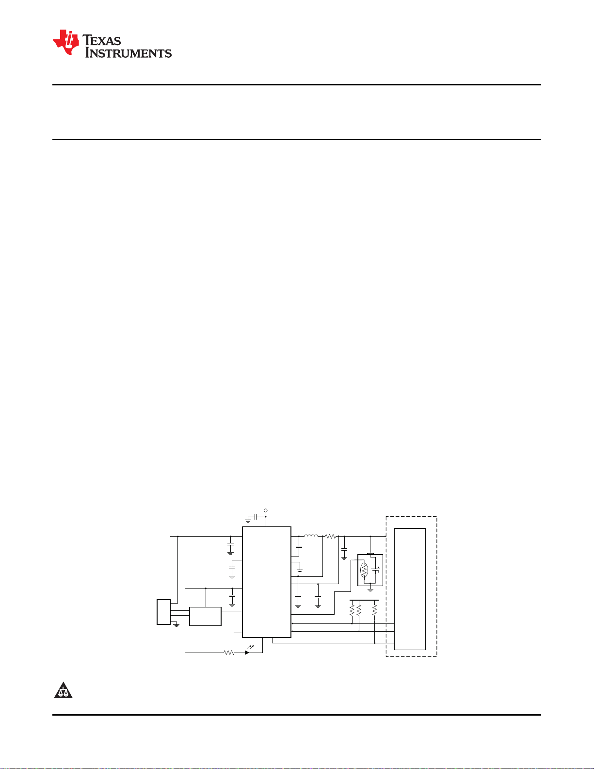
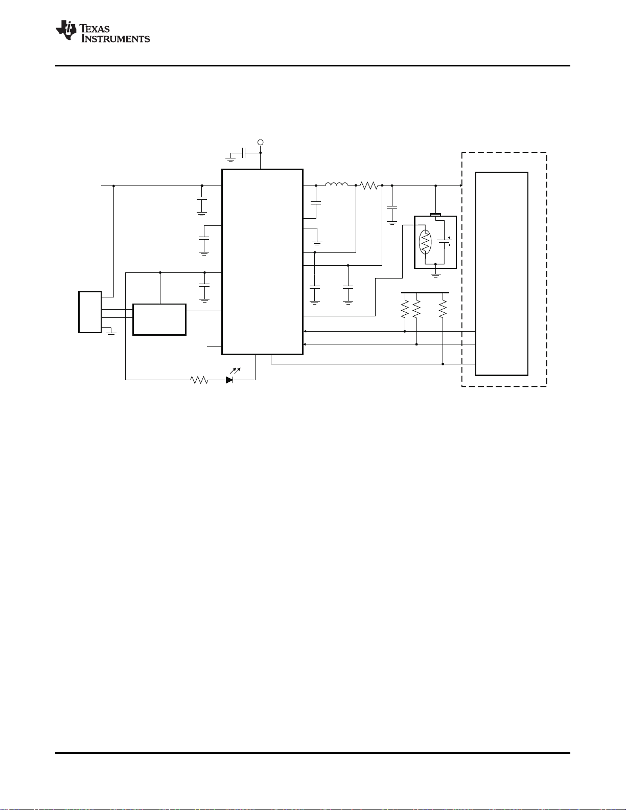
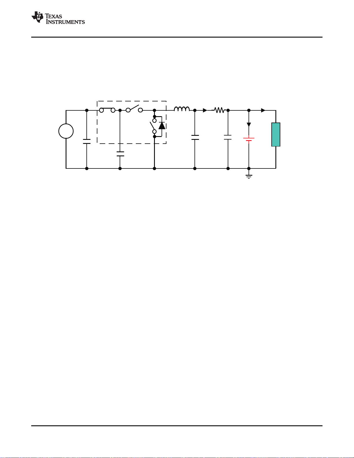
TYPICAL APPLICATION CIRCUITS
VBUS = 5V, I
IN_LIMIT
12 seconds watchdog
= 500mA, I
CHARGE
= 1A, V
SLUSA02 A –FEBRUARY 2010–REVISED FEBRUARY 2010
= 3.5--4.44V (Adjustable), Safety Timer = 27 minute default w/
BAT
Figure 2. I2C Controlled 1-Cell USB Charger Application Circuit
Copyright © 2010, Texas Instruments Incorporated Submit Documentation Feedback 9
Product Folder Link(s): bq24180
t-Time-4ms/div
V
VBUS
V
BAT
I
OUT
V
INT/ STAT
5V/div
500mA/div
5V/div
2V/div
“NoBattery” FaultInterrupt
V
BAT
I
OUT
V
INT/ STAT
5V/div
200mA/div
2V/div
t-Time-2s/div
t-Time-4ms/div
V
VBUS
V
INT/ STAT
20mA/div
1V/div
2V/div
V
VBUS
<3.8V
"Faulty Adapter"FaultInterrupt
I
VBUS
t-Time-4ms/div
V
VBUS
V
BAT
I
OUT
V
INT/ STAT
5V/div
500mA/div
5V/div
2V/div
V
VBUS
V
INT/ STAT
20mA/div
1V/div
2V/div
t-Time-1s/div
I
VBUS
"Faulty Adapter"FaultInterrupt
V
SW
I
L
500mA/div
2V/div
t-Time-2 s/divm
V =5V,
V =3.6V
VBUS
BAT
bq24180
SLUSA02 A –FEBRUARY 2010–REVISED FEBRUARY 2010
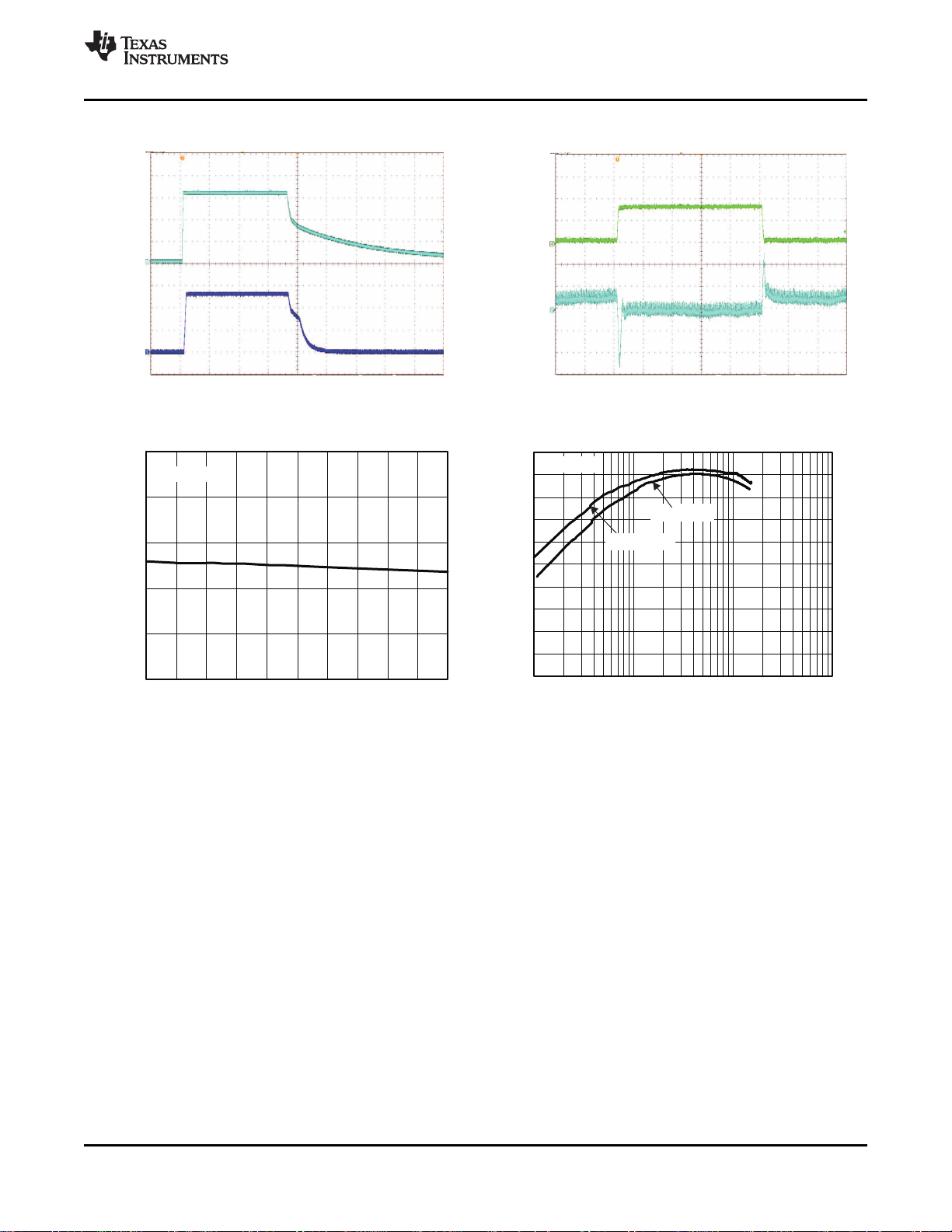
TYPICAL CHARACTERISTICS
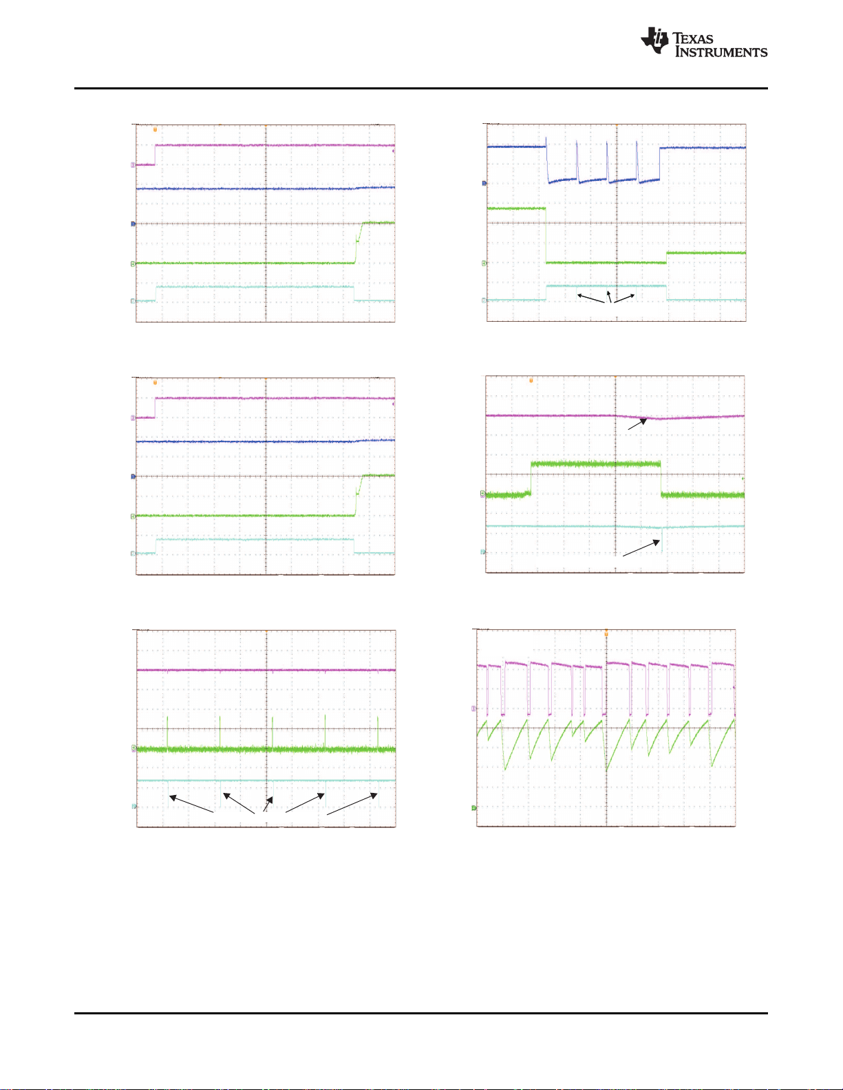
Figure 3. Adapter Insertion Figure 4. Battery Insertion/Removal
www.ti.com
Figure 5. PWM Charging Waveforms Figure 6. Faulty Adapter Detection
Figure 7. Faulty Adapter Detection Figure 8. Cycle by Cycle Current Limit
(Showing Continuous Detection)
Product Folder Link(s): bq24180
10 Submit Documentation Feedback Copyright © 2010, Texas Instruments Incorporated
I
VBUS
V
SW
V
BAT
1V/div
200mA/div
2V/div
t-Time-400 s/divm
I
VBUS
V
SW
1V/div
200mA/div
2V/div
t-Time-400 s/divm
V
BAT
V
SCL
I
OUT
200mA/div
1V/div
t-Time-200 s/divm
I
VBUS
V
SW
V
BAT
1V/div
200mA/div
2V/div
t-Time-400 s/divm
V
PSEL
V
BAT
200mA/div
1V/div
2V/div
t-Time-1ms/div
I
VBUS
V
VBUS
V
BAT
50mA/div
2V/div
1V/div
t-Time-10ms/div
I
VBUS
Faulty Adapter
Detection
bq24180
www.ti.com
SLUSA02 A –FEBRUARY 2010–REVISED FEBRUARY 2010
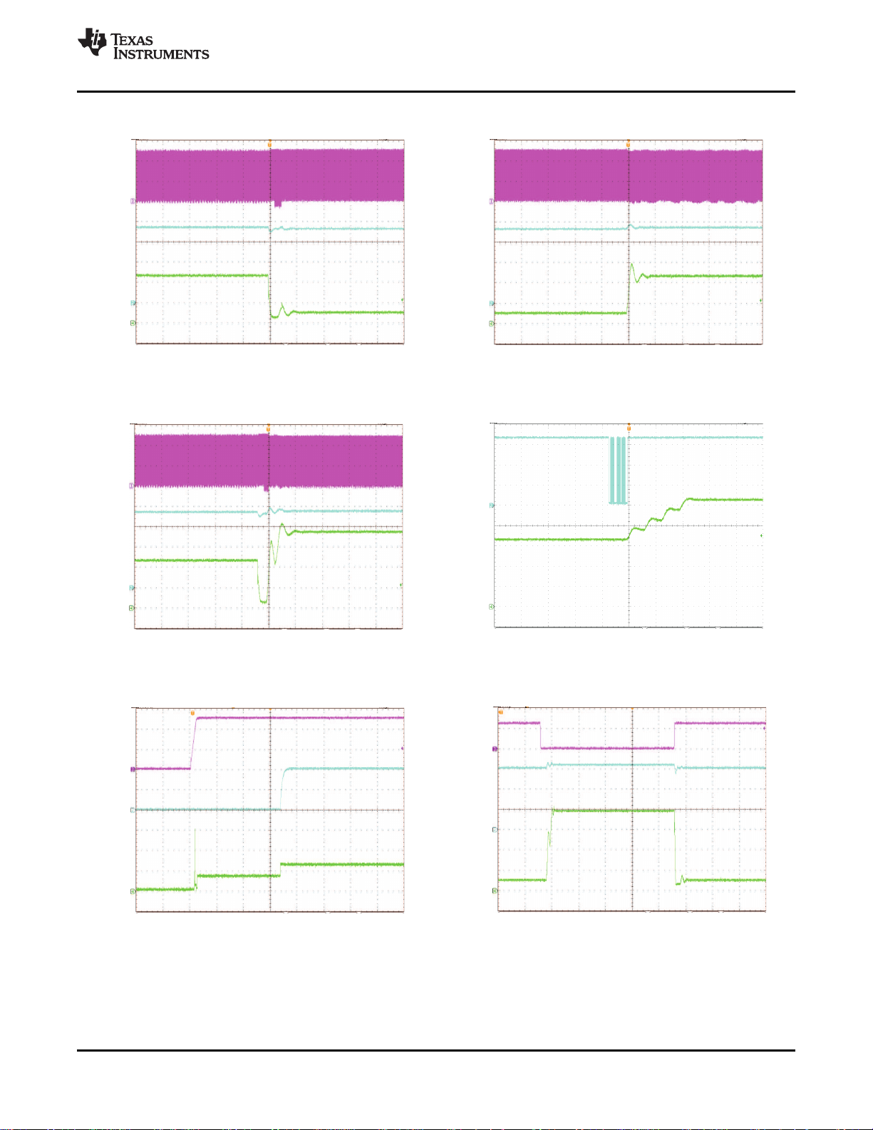
TYPICAL CHARACTERISTICS (continued)
Figure 9. Input Current Limit Transition Figure 10. Input Current Limit Transition
USB500 to USB100 USB100 to USB500
Figure 11. Input Current Limit Transition Figure 12. Charge Current Transition
USB500 to 750mA
Figure 13. Startup Into Default Mode Figure 14. PSEL Transition
No Battery Connected
Copyright © 2010, Texas Instruments Incorporated Submit Documentation Feedback 11
Product Folder Link(s): bq24180
550mA to 1.05A Using I2C
I
DCOUT
V
DCOUT
500mA/div
1V/div
t-Time-4ms/div
R =11 to1 ,
V =4V
LOAD
BAT
W W
I
VBUS
V
CD
V
BAT
1V/div
200mA/div
2V/div
t-Time-10ms/div
I
DCOUT
V
DCOUT
500mA/div
1V/div
t-Time-2ms/div
I
SW
I
OUT
5V/div
500mA/div
10V/div
t-Time-10 s/divm
V
VBUS
V
VBUS
=5.5Vto17V
V
SW
5V/div
500mA/div
5V/div
t-Time-10 s/divm
V
VBUS
I
OUT
TrickleCharge
USB100
V
VBUS
=5.5Vto10.5V
100
150
200
250
300
350
400
-40 -20 0 20 40 60 80 100 120 140
V -V
DO(VBUS-DRV)
T -Free-AirTemperature-°C
A
V =5V,
I =1 A,
I =10mA
VBUS
VBUS
DRV
bq24180
SLUSA02 A –FEBRUARY 2010–REVISED FEBRUARY 2010
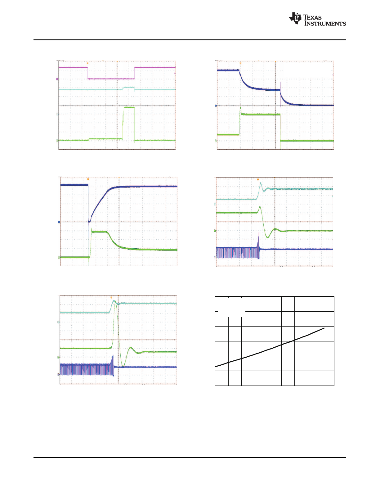
TYPICAL CHARACTERISTICS (continued)
Figure 15. Enable/Disable Using CD Figure 16. DCOUT OCP Response
www.ti.com
Figure 17. Hotplug 1000µF Capacitor into DCOUT Figure 18. OVP Response
12 Submit Documentation Feedback Copyright © 2010, Texas Instruments Incorporated
Figure 19. VINHIGH Response Figure 20. DRV Dropout vs T
A
Product Folder Link(s): bq24180
V
VBUS
V
DRV
2V/div
t-Time-2ms/div
2V/div
V
VBUS
=0Vto5.5Vto0V
I
DRV
10mA/div
t-Time-20 s/divm
V
DRV
5.1VOffset
10mV/div
0
10
20
30
40
50
60
70
80
90
100
0.01 0.1 1 10
Current- A
Efficiency-%
V
VBUS
=5V
V =3.5V
OUT
V =4.45V
OUT
5.05
5.07
5.09
5.11
5.13
5.15
0 1 2 3 4 5 6 7 8 9 10
I -mA
DRV
V -V
DRV
V =5.5V
BUS
bq24180
www.ti.com
SLUSA02 A –FEBRUARY 2010–REVISED FEBRUARY 2010
TYPICAL CHARACTERISTICS (continued)
Figure 21. DRV Startup/Shutdown Figure 22. DRV Load Transient
Figure 23. DRV Load Regulation Figure 24. Charger Efficiency
Copyright © 2010, Texas Instruments Incorporated Submit Documentation Feedback 13
Product Folder Link(s): bq24180

VUVLO < VIN < VOVP?
Yes
No
VBAT > 2V?
Yes
Enable 50mA
prechargecurrent
STAT = 0
No
BeginSafety Timer
V
HIGH<VIN<VOVP
No
Enable 50mA
prechargecurrent
Timer 2x
STAT = 0
Yes
Good Adapter
connected?
No
AdapterPlugIN
Watchdog TimerExpired
andNot Active, noactive
hostcommunication
Yes
BeginDEFAULT
ModeBattery
ChargeCycle
Wait 2s
bq24180
SLUSA02 A –FEBRUARY 2010–REVISED FEBRUARY 2010
www.ti.com
DETAILED DESCRIPTION
The bq24180 is a highly integrated synchronous switch-mode charger featuring integrated MOSFETs and small
external components, targeted at extremely space-limited portable applications powered by 1-cell Li-Ion or
Li-polymer battery pack. For current limited power source, such as a USB host or hub, the high efficiency
converter is critical in fully utilizing the input power capacity and quickly charging the battery. Due to the high
efficiency in a wide range of the input voltage and battery voltage, the switching mode charger is a good choice
for high speed charging with less power loss and better thermal management.
The bq24180 has two operation modes: charge mode and high impedance mode. In charge mode, the bq24180
supports a precision Li-ion or Li-polymer charging system for single-cell applications. In high impedance mode,
the bq24180 stops charging and operates in a mode with very low current from IN and battery, to effectively
reduce the power consumption when the portable device in standby mode. Through proper control, bq24180
achieves the smooth transition among different operation modes.
Charge Mode Operation
14 Submit Documentation Feedback Copyright © 2010, Texas Instruments Incorporated
Figure 25. Startup on Adapter Plug-In in DEFAULT Mode
Product Folder Link(s): bq24180

VUVLO < VIN < VOVP?
Yes
No
VBAT > 2V?
Enable 50mA
prechargecurrent
STAT = 0
No
/CEbit = 0?
No
Yes
BeginSafety Timer
V
HIGH<VIN<VOVP
No
Enable 50mA
prechargecurrent
Timer 2x
STAT = 0
Yes
Good Adapter
connected?
AdapterPlugIN
Watchdog Active
ActiveHost
Communication
Yes
BeginHOST
ModeBattery
Charging
Hi-Zbit = 0?
Yes
No
Wait 2s
No
EnableHi-ZMode
bq24180
www.ti.com
SLUSA02 A –FEBRUARY 2010–REVISED FEBRUARY 2010
Charge Profile
In charge mode, bq24180 has five control loops to regulate input voltage, input current, charge current, charge
voltage and device junction temperature. During the charging process, all five loops are enabled and the one that
is dominant will take over the control. The bq24180 supports a precision Li-ion or Li-polymer charging system for
single-cell applications. Figure 27 indicates a typical charge profile without input current regulation loop and it is
similar to the traditional CC/CV charge curve, while Figure 27 shows a typical charge profile when input current
limiting loop is dominant during the constant current mode, and in this case the charge current is higher than the
input current so the charge process is faster than the linear chargers. For bq24180, the input current limits, the
charge current, termination current, and charge voltage are all programmable using I2C interface.
Figure 26. Startup on Adapter Plug-In in Host-Controlled Mode
Copyright © 2010, Texas Instruments Incorporated Submit Documentation Feedback 15
Product Folder Link(s): bq24180

Precharge
(LinearCharge)
FastCharge
(PWMCharge)
I
SHORT
Termination
V
SHORT
Regulation
Current
Regulation
voltage
Precharge
Phase
CurrentRegulation
Phase
VoltageRegulation
Phase
ChargeCurrent
ChargeVoltage
(a)Withoutinputcurrentlimit(defaultwhenPSEL =1)
Precharge
(LinearCharge)
FastCharge
(PWMCharge)
I
SHORT
Termination
V
SHORT
Regulation
voltage
Precharge
Phase
CurrentRegulation
Phase
VoltageRegulation
Phase
ChargeCurrent
ChargeVoltage
(b)Withinputcurrentlimit(defaultwhenPSEL =0)
bq24180
SLUSA02 A –FEBRUARY 2010–REVISED FEBRUARY 2010
www.ti.com
Figure 27. Typical Charging Profile of bq24180
PWM Controller in Charge Mode
The bq24180 provides an integrated, fixed 3 MHz frequency voltage-mode controller with Feed-Forward function
to regulate charge current or voltage. This type of controller is used to help improve line transient response,
thereby simplifying the compensation network used for both continuous and discontinuous current conduction
operation. The voltage and current loops are internally compensated using a Type-III compensation scheme that
provides enough phase margin for stable operation, allowing the use of small ceramic capacitors with very low
ESR. There is a 0.5V offset on the bottom of the PWM ramp to allow the device to operate between 0% to 99.5%
duty cycles.
The bq24180 has two back to back common-drain N-channel MOSFETs at the high side and one N-channel
MOSFET at low side. An input N-MOSFET (Q1) prevents battery discharge when VBUS is lower than V
The second high-side N-MOSFET (Q2) behaves as the switching control switch (see Figure 1). A charge pump
circuit is used to provide gate drive for Q1, while a boot strap circuit with external boot-strap capacitor is used to
boost up the gate drive voltage for Q2.
VBUS (MIN)
.
16 Submit Documentation Feedback Copyright © 2010, Texas Instruments Incorporated
Product Folder Link(s): bq24180

bq24180
www.ti.com
SLUSA02 A –FEBRUARY 2010–REVISED FEBRUARY 2010
Cycle-by-cycle current limit is sensed through the internal sense MOSFETs for Q2 and Q3. The threshold for Q2
is set to a nominal 2.5-A peak current. The low-side MOSFET (Q3) also has a current limit that decides if the
PWM Controller will operate in synchronous or non-synchronous mode. This threshold is set to 100mA and it
turns off the low-side N-channel MOSFET (Q3) before the current reverses, preventing the battery from
discharging. Synchronous operation is used when the current of the low-side MOSFET is greater than 100mA to
minimize power losses.
Battery Charging Process
At the beginning of precharge, while battery voltage is below the V
50mA precharge current, I
PRECHARGE
When the battery voltage is above V
current, I
OCHARGE
, or a charge current that corresponds to the input current of I
, to the battery.
PRECHARGE
and below V
PRECHARGE
, the charge current ramps up to fast charge
OREG
charge current is controlled to minimize the current and voltage over-shoot during transient. The input current
limit, I
to the regulation voltage, V
, and fast charge current, I
IN_LIMIT
OCHARGE
, the charge current is tapered down as shown in Figure 27. The voltage
OREG
, are programmable by the host. Once the battery voltage is close
regulation feedback occurs by monitoring the battery-pack voltage between the CSOUT and PGND pins. The
bq24180 is a fixed single-cell voltage version, with adjustable regulation voltage (3.5V to 4.44V) programmed
using the I2C interface.
The bq24180 monitors the charging current during the voltage regulation phase. Once the termination threshold,
I
, is detected and the battery voltage is above the recharge threshold, the bq24180 terminates charge. The
TERM
termination current level is programmable. To disable the charge current termination, the host sets the charge
termination bit (TE) of charge control register to 0, refer to I2C section for details.
A new charge cycle is initiated when one of the following conditions is detected:
1. The battery voltage falls below the V
OREG-VRCH
2. VBUS Power-on reset (POR), if battery voltage is below the V
threshold.
PRECHARGE
3. CE bit toggle or RESET bit is set (Host controlled)
threshold, the bq24180 applies the
. The slew rate for fast
IN_LIMIT
threshold
Copyright © 2010, Texas Instruments Incorporated Submit Documentation Feedback 17
Product Folder Link(s): bq24180

ChargeDone?
I
CHG
< I
TERM
No
Start 32 second
watchdogtimer
32stimerexpired?
No
Yes
ReceivedSWwatchdog
RESET?
No
Yes
Yes
Reset 32 second
watchdogtimer
Safetytimer
fault
Chargingsuspended
Entersuspended
mode
Faultindicatedin
STAT registers
Safety Timerexpired?
No
Yes
HOST ModeBattery
Charging
BeginDEFAULT
ModeBattery
ChargeCycle
CVMode?
No
TermEnabled?
Yes
Yes
No
STAT = Hi
UpdateSTAT
bits
Terminate
Safety Timer
BatteryPresent?
Yes
Indicate
BatteryNot
PresentFault
ResetI2Cto
default
V
BAT<VRCH
?
No
DEFAULTMode ?
Yes
Indicate TimerFault
ResetI2Ctodefault
Begin
DEFAULT
ModeBattery
ChargeCycle
BeginHOST
ModeBattery
Charging
Yes
No
bq24180
SLUSA02 A –FEBRUARY 2010–REVISED FEBRUARY 2010
www.ti.com
DEFAULT Mode
DEFAULT mode is used when I2C communication is not available. DEFAULT mode is entered in the following
situations:
1. When the charger is enabled and V
2. When the watchdog timer expires without a reset from the I2C interface and the safety timer has not expired.
3. When the device comes out of any fault condition (sleep mode, OVP, faulty adapter mode, etc.) before I2C
communication is established
In default mode, the I2C registers are reset to the default values. The 27 min safety timer is reset and starts when
DEFAULT mode is entered. The default value for V
input current limit is determined by the PSEL input. If PSEL selects adapter mode, there is no input current limit.
If PSEL selects PC mode, the input current limit is set to 100mA. Default mode is exited by programming the I2C
interface. Startup into DEFAULT mode is shown in Figure 29. Note that if termination is enabled and charging
has terminated, a new charge cycle is NOT initiated when entering DEFAULT mode.
Figure 28. Host Mode Charging Process
>3.6V before I2C communication is established
BAT
OREG
is 3.6V, and the default value for I
CHARGE
18 Submit Documentation Feedback Copyright © 2010, Texas Instruments Incorporated
Product Folder Link(s): bq24180
is 1A. The

PSEL = Hi?
No
Yes
PCMode
LoadPCdefault
valuesforinput
currentlimitfromI2C
registers.
STAT = 0
AC Adapter
Mode
(AAM)
Loaddefaultvaluesto
I2Cregisters.
NoInputCurrentLimit
STAT = 0
No
Yes
Safety Timerexpired?
No
Yes
Safetytimer
fault
Chargingsuspended
Entersuspended
mode
Faultindicatedin
STAT registers
BeginDEFAULT
ModeBattery
ChargeCycle
BeginHOST Mode
BatteryCharging
LoadOptimizedCharge
Parameters?
No
Resetsafetytimerto
27minandstart
bq24180
www.ti.com
SLUSA02 A –FEBRUARY 2010–REVISED FEBRUARY 2010
Safety Timer and Watchdog Timer in Charge Mode
At the beginning of charging process, the bq24180 starts the safety timer. This timer is active during the entire
charging process. If charging has not terminated before the safety timer expires, the IC enters suspend mode
where charging is halted. The safety timer time is selectable using the I2C interface. A single 128µs pulse is sent
on the STAT and INT outputs and the STATx bits of the status registers are updated in the I2C. The EN bit or
power must be toggled in order to clear the safety timer fault. The safety timer duration is selectable using the
TMR_X bits in the V
timer.
In addition to the safety timer, the bq24180 contains a watchdog timer that monitors the host through the I2C
interface. Once a read/write is performed on the I2C interface, a 12-second timer (t
12-second timer is reset by the host using the I2C interface. This is done by writing a "1" to the reset bit
(TMR_RST) in the control register. The TMR_RST bit is automatically set to “0” when the 12-second timer is
reset. This process continues until battery is fully charged or the safety timer expires. If the 12-second timer
expires, the IC enters DEFAULT mode where the default charge parameters are loaded, the safety timer restarts
at 27 minutes and charging continues. The I2C may be accessed again to reinitialize the desired values and
restart the watchdog timer as long as the 27 minute safety timer has not expired. Once the safety timer expires,
charging is disabled. This function prevents continuous charging of a defective battery if the host fails to reset the
safety timer. The watchdog timer flow chart is shown in Figure 30.
Copyright © 2010, Texas Instruments Incorporated Submit Documentation Feedback 19
Figure 29. DEFAULT Mode Charging Process
Voltage/ Safety Timer Register. Changing the safety timer duration resets the safety
IN-DPM
WATCHDOG
Product Folder Link(s): bq24180
) is started. The

StartSafety Timer
ChargeDone?
I
CHG
< I
TERM
No
STAT = Hi
UpdateSTAT
bits
I2CRead/Write
performed?
Start 12 second
watchdogtimer
No
Yes
12stimerexpired?
No
Yes
ReceivedSWwatchdog
RESET?
No
Yes
Safetytimerexpired?
No
Yes
Safetytimer
fault
Chargingsuspended
Entersuspended
mode
Faultindicatedin
STAT registers
Yes
ChargeDone?
I
CHG
< I
TERM
No
STAT = Hi
UpdateSTAT
bits
Yes
Reset 12 second
watchdogtimer
Resettodefault
valuesinI2C
register
Restart 27min
safetytimer
Safetytimerexpired?
Safetytimer
fault
Chargingsuspended
Entersuspended
mode
Faultindicatedin
STAT registers
No
Yes
bq24180
SLUSA02 A –FEBRUARY 2010–REVISED FEBRUARY 2010
www.ti.com
Figure 30. The Watchdog Timer Flow Chart for bq24180
Power Source Selector Input (PSEL)
The bq24180 contains a PSEL input that is used to program the input current limit during DEFAULT mode. Drive
PSEL high to indicate a USB source is connected to the input and the PC mode default values should be used.
When PSEL is high, the IC starts up with a 100mA input current limit and a 1A charge current. Drive PSEL low to
indicate that an AC Adapter is connected to the input. When PSEL is high, the IC starts up with no input current
limit and a 1A charge current. PSEL is internally pulled up to the DRV supply with a 100kΩ resistor.
20 Submit Documentation Feedback Copyright © 2010, Texas Instruments Incorporated
Product Folder Link(s): bq24180

bq24180
www.ti.com
SLUSA02 A –FEBRUARY 2010–REVISED FEBRUARY 2010
Hardware Disable Input (CD)
The bq24180 contains a CD input that is used to disable the charger and place the bq24180 into high-impedance
mode. Drive CD low to enable charge and enter normal operation. Drive CD high to disable charge and place the
bq24180 into high-impedance mode. Driving CD high during DEFAULT mode resets the safety timer. Driving CD
high during HOST mode suspends, but does NOT reset the safety timer. CD is internally pulled down to GND
with a 100kΩ resistor.
LDO Output (DRV)
The bq24180 contains a linear regulator (DRV) that is used to supply the internal MOSFET drivers and other
circuitry. Additionally, DRV supplies up to 10mA external loads to power the STAT LED or the USB transceiver
circuitry. The maximum value of the DRV output is 5.5V so it ideal to protect voltage sensitive USB circuits. The
LDO is on whenever a VBUS supply is connected to the bq24180. The DRV is disabled under the following
conditions:
1. Faulty adapter detected or VBUS < UVLO
2. Thermal Shutdown
AC Adapter Mode, Charge Current Limiting
After power is connected and startup is initiated, the PSEL input is read to determine the default startup values. If
PSEL is 0, AC Adapter mode is selected. In AC Adapter mode, the charge current is regulated to maximize the
charging time. The default parameters in AC Adapter mode are I
may be changed at any time using the I2C interface. Additionally, if input current monitoring is required, this may
be used during AC Adapter mode as well, but is disabled in DEFAULT mode.
CHARGE
=1A and V
=3.6V. These values
OUTREG
PC Mode, Input Current Limiting
After power is connected and startup is initiated, the PSEL input is read to determine the default startup values.
In PC mode, the input current is limited to maximize the charge rate of bq24180 without overloading the USB
port. The input current for bq24180 can be limited to 100mA, 500mA or 800mA and is programmed in the control
register. Once the input current reaches the input current limiting threshold, the charge current is reduced to
prevent the input current from exceeding the programmed threshold. The input current sensing resistor and
control loop are integrated into bq24180. The input current limit is disabled using I2C control; refer to the
definition of control register (01H) for detail. The default parameters in USB mode are I
V
=3.6V. Charge current may be monitored in PC mode as well, but by default it is set to a maximum such
OUTREG
=100mA and
INLIM
that the input current limit loop is active.
DCOUT Functionality
The bq24180 contains a DCOUT function that is used to connect a load to the battery through a switch. DCOUT
is implemented using back to back MOSFETs (Q4 and Q5 in Figure 1) to connect DCOUT to the battery. This
prevents reverse feeding the battery from DCOUT when DCOUT is disabled. DCOUT is a current limited source
and can provide up to 1A to power additional accessories. The current limit is programmable from 370mA to 1.5A
in 4 steps using the I2C interface. Additionally, the DCOUT output is enabled or disabled using the I2C interface.
If the load on DCOUT reaches the current limit, the FET that connects DCOUT to the battery is turned off after
the deglitch time (t
dgl_DCOUT
), a single 128µs pulse is sent on the STAT and INT outputs and the FAULT_x bits of
the status register are updated in the I2C. The DCOUT may be enabled after the fault using the I2C interface.
External NTC Monitoring (TS)
The bq24180 provides a TS input for monitoring an external NTC thermistor. A current is sourced to the NTC
from the TS input and the voltage is monitored. There are 3 temperature thresholds that are monitored; the cold
battery threshold (T
(T
> 55°C). These temperatures correspond to the V
NTC
NTC thermistor (b=3500). The TS input is monitored at all times, however, it only affects charging during default
mode. During default mode, charging is suspended and timers are suspended when T
When 45°C < T
NTC
remains at 100mA in this mode.
< 5°C), the warm battery threshold (45°C < T
NTC
HOT
, V
WARM
< 55°C) and the hot battery threshold
NTC
, and V
thresholds when using a 4.7kΩ
COLD
< 5°C or T
NTC
NTC
> 55°C.
< 55°C, the charging current is reduced to 400mA (max). In PC mode, the charge current
Copyright © 2010, Texas Instruments Incorporated Submit Documentation Feedback 21
Product Folder Link(s): bq24180

400 mA
T 1
(5ºC)
T 2
(45ºC)
T 3
(55ºC)
1A
bq24180
TS
TEMP
PACK+
PACK-
+
+
V
HOT
V
COLD
I
NTC
+
V
WARM
bq24180
SLUSA02 A –FEBRUARY 2010–REVISED FEBRUARY 2010
www.ti.com
Figure 31. Charge Current During TS Conditions in Default Mode
When the bq24180 is not in default mode, the TS input is monitored and faults are displayed in the I2C registers.
If any of the 3 TS fault conditions occur, a single 128µs pulse is sent on the STAT and INT outputs and the
STATx and FAULT_x bits of the status registers are updated in the I2C. The FAULT_x bits signal a general
temperature fault. The TS_FAULTX bits in the NTC Monitor Register show the exact TS fault that has occurred.
Figure 32. TS Circuit
Thermal Regulation and Protection
During the charging process, to prevent overheat of the chip, bq24180 monitors the junction temperature, TJ, of
the die and begins to taper down the charge current once TJreaches the thermal regulation threshold, TCF. The
charge current is reduced to zero when the junction temperature increases about 10°C above TCF. At any state, if
TJexceeds T
shutdown mode, PWM is turned off, all timers are terminated and reset, and a single 128µs pulse is sent on the
STAT and INT outputs and the STATx and FAULT_x bits of the status registers are updated in the I2C. A new
charging cycle begins when TJfalls below T
after a thermal shutdown fault.
22 Submit Documentation Feedback Copyright © 2010, Texas Instruments Incorporated
SHTDWN
, bq24180 terminates charging and disables DCOUT in the I2C register. During thermal
SHTDWN
Product Folder Link(s): bq24180
by approximately 10°C. DCOUT must be enabled by the host

bq24180
www.ti.com
SLUSA02 A –FEBRUARY 2010–REVISED FEBRUARY 2010
Input Voltage Protection in Charge Mode
Sleep Mode
The bq24180 enters the low-power sleep mode if the voltage on V
threshold, V
CSOUT+VSLP
prevents draining the battery during the absence of V
, and V
is higher than the undervoltage lockout threshold, V
VBUS
. During sleep mode, both the reverse blocking
VBUS
switch Q1 and PWM are turned off. Once the input rises above the sleep threshold, the device returns to
normal operation.
Input Voltage Based DPM
During normal charging process, if the input power source is not able to support the programmed or default
charging current, VBUS voltage will decease. Once the VBUS drops to V
current is tapered down to prevent the further drop of VBUS. When the IC enters this mode, the charge
current is lower than the set value and the DPM_STATUS bit is set (B4 in Register 05H). This feature
ensures IC compatibility with adapters with different current capabilities.
Faulty Adapter Detection
When an input source is connected to the bq24180, the device enter faulty adapter detection mode. In this
mode, the IC sources 30mA to the battery for t
the device continues the startup sequence. If V
. After t
INT
VBUS<VIN(MIN)
, the input voltage is monitored. If V
INT
, a single 128µs pulse is sent on the STAT and
INT outputs and the STATx and FAULT_x bits of the status registers are updated in the I2C and the process
repeats until a good adapter is detected.
High-Input and Input Over-Voltage Protection
The bq24180 provides two levels over-voltage protection on the input. A high-input comparator disables the
PWM operation and sources the 50mA precharge current to the battery when V
allows for unregulated adapters to be used. The 50mA pulls the adapter voltage down to the usable voltage
and then normal operation begins.
The built-in input over-voltage protection to protect the device and other components against damage from
overvoltage on the input supply (Voltage from V
to PGND). When V
VBUS
the PWM converter, a single 128µs pulse is sent on the STAT and INT outputs and the STATx and FAULT_x
bits of the status registers are updated in the I2C. Once the OVP fault is removed, the STATx and FAULT_x
bits are cleared and the device returns to normal operation.
falls below sleep-mode entry
VBUS
UVLO
VBUS_LOW
VBUS
(default 4.76V), the charge
< V
> V
HIGH
, the bq24180 latches off
OVP
VBUS
. This feature
VBUS>VIN(MIN)
< V
OVP
,
. This
Charge Status Outputs (STAT, INT)
The STAT and INT outputs are used to indicate operation conditions for bq24180. STAT and INT are pulled low
during charging when EN_STAT bit in the control register (00H) is set to “1”. When charge is complete or
disabled, INT and STAT are high impedance. When a fault occurs, a 128-µs pulse (interrupt) is sent out to notify
the host. The status of STAT and INT during different operation conditions is summarized in Table 1. STAT
drives an LED for visual indication. INT is available for connecting to the logic rail for host communication.
Table 1. STAT Pin Summary
CHARGE STATE STAT and INT BEHAVIOR
Charge in progress and EN_STAT=1 Low
Other normal conditions Open-drain
Charge mode faults: Timer fault, sleep mode, 128-µs pulse, then open-drain
VBUS over voltage, VBUS UVLO, thermal
shutdown
Control Bits in Charge Mode
CE Bit (Charge Enable)
The bit of CE in control register is used to disable or enable the charge process. A low logic level (0) on this
bit enables the charge and a high logic level (1) disables the charge.
RESET Bit
Copyright © 2010, Texas Instruments Incorporated Submit Documentation Feedback 23
Product Folder Link(s): bq24180

o
OU T OU T
1
=
2 L C
¦
´ ´p
ITERM0
OT ERM_STE P
SN S
V
I =
R
ICHR G0
OCHARG E_STEP
SNS
V
I =
R
bq24180
SLUSA02 A –FEBRUARY 2010–REVISED FEBRUARY 2010
www.ti.com
The bit of RESET in control register is used to reset all the charge parameters. Write ‘1” to RESET bit to
reset all the charge parameters to default values and RESET bit is automatically cleared to zero once the
charge parameters get reset. It is designed for charge parameter reset before charge starts and it is not
recommended to set RESET bit when charging or boosting in progress.
Output Inductor and Capacitor Selection Guidelines
The bq24180 provides internal loop compensation. With this scheme, best stability occurs when LC resonant
frequency, of, is approximately 40 kHz (20 kHz to 80 kHz). Equation 1 can be used to calculate the value of the
output inductor, L
, and output capacitor, C
OUT
OUT
.
(1)
To reduce the output voltage ripple, a ceramic capacitor with the capacitance between 4.7µF and 47µF is
recommended for C
, refer to the application section for components selection.
OUT
Selecting Current Sense Resistor
Both the termination current range and charge current range are depending on the sensing resistor (R
termination current step (I
OTERM_STEP
) can be calculated using Equation 2:
Table 2 shows the termination current settings with two sensing resistors.
SNS
). The
(2)
Table 2. Termination Current Settings for 68mΩ and 100mΩ Sense Resistors
BIT V
V
ITERM2
V
ITERM1
V
ITERM0
Offset 1.7 25 17
The charge current step (I
OCHARGE_STEP
) can be calculated using Equation 3:
(mV) I
ITERM
6.8 100 68
3.4 50 43
1.7 25 17
TERM
R
= 68 mΩ R
SNS
Table 3 shows the charge current settings with two sensing resistors.
Table 3. Charge Current Settings for 68 mΩ and 100 mΩ Sense Resistors
BIT V
V
ICHRG3
V
ICHRG2
V
ICHRG1
V
ICHRG0
Offset 37.4 550 374
(mV) I
IREG
54.4 800 544
27.2 400 272
13.6 200 136
6.8 100 68
OCHARGE
R
= 68 mΩ R
SNS
(mA) I
(mA) I
TERM
= 100 mΩ
SNS
OCHARGE
= 100 mΩ
SNS
(mA)
(3)
(mA)
24 Submit Documentation Feedback Copyright © 2010, Texas Instruments Incorporated
Product Folder Link(s): bq24180

DATA
CLK
STARTCondition STOP Condition
DATA
CLK
DataLine
Stable;
DataValid
Charge
ofData
Allowed
bq24180
www.ti.com
SLUSA02 A –FEBRUARY 2010–REVISED FEBRUARY 2010
SERIAL INTERFACE DESCRIPTION
I2C is a 2-wire serial interface developed by Philips Semiconductor (see I2C-Bus Specification, Version 2.1,
January 2000). The bus consists of a data line (SDA) and a clock line (SCL) with pull-up structures. When the
bus is idle, both SDA and SCL lines are pulled high. All the I2C compatible devices connect to the I2C bus
through open drain I/O pins, SDA and SCL. A master device, usually a microcontroller or a digital signal
processor, controls the bus. The master is responsible for generating the SCL signal and device addresses. The
master also generates specific conditions that indicate the START and STOP of data transfer. A slave device
receives and/or transmits data on the bus under control of the master device.
The bq24180 device works as a slave and is compatible with the following data transfer modes, as defined in the
I2C Bus™ Specification: standard mode (100 kbps), fast mode (400 kbps), and high-speed mode (up to 3.4 Mbps
in write mode). The interface adds flexibility to the battery charge solution, enabling most functions to be
programmed to new values depending on the instantaneous application requirements. Register contents remain
intact as long as battery voltage remains above 2.5 V (typical). The I2C circuitry is powered from VBUS when a
supply is connected. If the VBUS supply is not connected, the I2C circuitry is powered from the battery through
CSOUT. The battery voltage must stay above 2.5V with no input connected in order to maintain proper operation.
The data transfer protocol for standard and fast modes is exactly the same; therefore, they are referred to as the
F/S-mode in this document. The protocol for high-speed mode is different from the F/S-mode, and it is referred to
as the HS-mode. The bq24150/1 device only supports 7-bit addressing. The device 7-bit address is defined as
‘1101011’ (6BH).
F/S Mode Protocol
The master initiates data transfer by generating a start condition. The start condition is when a high-to-low
transition occurs on the SDA line while SCL is high, as shown in Figure 33. All I2C -compatible devices should
recognize a start condition.
Figure 33. START and STOP Condition
The master then generates the SCL pulses, and transmits the 8-bit address and the read/write direction bit R/W
on the SDA line. During all transmissions, the master ensures that data is valid. A valid data condition requires
the SDA line to be stable during the entire high period of the clock pulse (see Figure 34). All devices recognize
the address sent by the master and compare it to their internal fixed addresses. Only the slave device with a
matching address generates an acknowledge (see Figure 34) by pulling the SDA line low during the entire high
period of the ninth SCL cycle. Upon detecting this acknowledge, the master knows that communication link with a
slave has been established.
Figure 34. Bit Transfer on the Serial Interface
The master generates further SCL cycles to either transmit data to the slave (R/W bit 1) or receive data from the
slave (R/W bit 0). In either case, the receiver needs to acknowledge the data sent by the transmitter. So an
acknowledge signal can either be generated by the master or by the slave, depending on which one is the
Copyright © 2010, Texas Instruments Incorporated Submit Documentation Feedback 25
Product Folder Link(s): bq24180

DataOutput
byTransmitter
DataOutput
byReceiver
SCL From
Master
START
Condition
ClockPulsefor
Acknowledgement
Not Acknowledge
Acknowledge
bq24180
SLUSA02 A –FEBRUARY 2010–REVISED FEBRUARY 2010
www.ti.com
receiver. the 9-bit valid data sequences consisting of 8-bit data and 1-bit acknowledge can continue as long as
necessary. To signal the end of the data transfer, the master generates a stop condition by pulling the SDA line
from low to high while the SCL line is high (see Figure 35). This releases the bus and stops the communication
link with the addressed slave. All I2C compatible devices must recognize the stop condition. Upon the receipt of
a stop condition, all devices know that the bus is released, and wait for a start condition followed by a matching
address. If a transaction is terminated prematurely, the master needs sending a STOP condition to prevent the
slave I2C logic from remaining in a incorrect state. Attempting to read data from register addresses not listed in
this section will result in FFh being read out.
Figure 35. Acknowledge on the I2C Bus
Figure 36. Bus Protocol
F/S Mode Protocol
When the bus is idle, both SDA and SCL lines are pulled high by the pull-up devices.
The master generates a start condition followed by a valid serial byte containing HS master code '00001XXX'.
This transmission is made in F/S mode at no more than 400 Kbps. No device is allowed to acknowledge the HS
master code, but all devices must recognize it and switch their internal setting to support 3.4-Mbps operation.
26 Submit Documentation Feedback Copyright © 2010, Texas Instruments Incorporated
Product Folder Link(s): bq24180

bq24180
www.ti.com
SLUSA02 A –FEBRUARY 2010–REVISED FEBRUARY 2010
The master then generates a repeated start condition (a repeated start condition has the same timing as the start
condition). After this repeated start condition, the protocol is the same as F/S mode, except that transmission
speeds up to 3.4 Mbps are allowed. A stop condition ends the HS mode and switches all the internal settings of
the slave devices to support the F/S mode. Instead of using a stop condition, repeated start conditions should be
used to secure the bus in HS mode. If a transaction is terminated prematurely, the master needs sending a
STOP condition to prevent the slave I2C logic from remaining in a incorrect state.
Attempting to read data from register addresses not listed in this section results in FFh being read out.
Copyright © 2010, Texas Instruments Incorporated Submit Documentation Feedback 27
Product Folder Link(s): bq24180

bq24180
SLUSA02 A –FEBRUARY 2010–REVISED FEBRUARY 2010
www.ti.com
REGISTER DESCRIPTION
blank paragraph for spacer
Status/Control Register (READ/WRITE) – Memory location: 00, Reset state: x1xx 0xxx
BIT NAME Read/Write FUNCTION
B7(MSB) TMR_RST Read/Write Write: TMR_RST function, write "1" to reset the watchdog timer (auto clear)
B6 EN_STAT Read/Write 1-Enable STAT function, 0-Disable STAT function (default 1)
B5 STAT2 Read only
B4 STAT1 Read only
B3 NA Read only NA
B2 FAULT_3 Read only
B1 FAULT_2 Read only VBUS<V
B0(LSB) FAULT_1 Read only
blank paragraph for spacer
Control Register (READ/WRITE) – Memory location: 01, Reset state: 0011 0000
BIT NAME Read/Write FUNCTION
B7(MSB) Iin_Limit_2 Read/Write 00-USB host with 100-mA current limit, 01-USB host with 500-mA current limit, 10-USB
B6 Iin_Limit_1 Read/Write
B5 DCOUT_ILIM1 Read/Write 00-DCOUT 350mA current limit, 01- DCOUT 750mA current limit, 10- DCOUT 1050mA
B4 DCOUT_ILIM2 Read/Write
B3 TE Read/Write 1-Enable charge current termination, 0-Disable charge current termination (default 0)
B2 CE Read/Write 1-Charger is disabled, 0-Charger enabled (default 0)
B1 HZ_MODE Read/Write 1-High impedance mode, 0-Not high impedance mode (default 0)
B0 (LSB) DCOUT_EN Read/Write 1-DCOUT Enabled, 0-DCOUT Disabled. (default 0)
(1) When in DEFAULT mode, the PSEL input determines the input current limit.
Read: 0 – PSEL indicates low, 1- PSEL indicates high
00-Ready, 01-Charge in progress, 10-Charge done, 11-Fault
Charge mode: 000-Normal, 001-VBUS OVP, 010-Sleep mode, 011- Faulty Adapter or
110-Timer fault, 111-No battery
host/charger with 800-mA current limit, 11-No input current limit (default 00
current limit, 11- DCOUT 1400mA current limit (default 11)
, 100-DCOUT Current Limit tripped, 101-Thermal shutdown or TS Fault,
UVLO
(1)
)
Control/Battery Voltage Register (READ/WRITE) – Memory location: 02, Reset state: 0001 01XX
BIT NAME Read/Write FUNCTION
B7(MSB) V
B6 V
B5 V
B4 V
B3 V
B2 V
B1 NA Read/Write NA
B0(LSB) NA Read/Write NA
OREG5
OREG4
OREG3
OREG2
OREG1
OREG0
Read/Write Battery Regulation Voltage: 640mV (default 0)
Read/Write Battery Regulation Voltage: 320mV (default 0)
Read/Write Battery Regulation Voltage: 160mV (default 0)
Read/Write Battery Regulation Voltage: 80mV (default 1)
Read/Write Battery Regulation Voltage: 40mV (default 0)
Read/Write Battery Regulation Voltage: 20mV (default 1)
blank paragraph for spacer
• Charge voltage range is 3.5V–4.44V with the offset of 3.5V and step of 20mV (default 3.6V).
blank paragraph for spacer
28 Submit Documentation Feedback Copyright © 2010, Texas Instruments Incorporated
Product Folder Link(s): bq24180

bq24180
www.ti.com
Vender/Part/Revision Register (READ only) – Memory location: 03, Reset state: 0100 0000
BIT NAME Read/Write FUNCTION
B7(MSB) Vender2 Read only Vender Code: bit 2 (default 0)
B6 Vender1 Read only Vender Code: bit 1 (default 1)
B5 Vender0 Read only Vender Code: bit 0 (default 0)
B4 PN1 Read only
B3 PN0 Read only
B2 Revision2 Read only
B1 Revision1 Read only
B0(LSB) Revision0 Read only
For I2C Address 6BH: 00 – bq24180
000: Revision 1.0; 001: Revision 1.1
010-111: Future Revisions
Battery Termination/Fast Charge Current Register (READ/WRITE)
Memory location: 04, Reset state: 1010 1011
BIT NAME Read/Write FUNCTION
B7(MSB) Reset Write only Write: 1-Charger in reset mode, 0-No effect
B6 V
B5 V
B4 V
B3 V
B2 V
B1 V
B0(LSB) V
ICHRG3
ICHRG2
ICHRG1
ICHRG0
ITERM2
ITERM1
ITERM0
Read/Write Charge current sense voltage: 54.4mV— (default 0)
Read/Write Charge current sense voltage: 27.2mV—(default 1)
Read/Write Charge current sense voltage: 13.6mV— (default 0)
Read/Write Charge current sense voltage: 6.8mV (default 1)
Read/Write Termination current sense voltage: 6.8mV (default 0)
Read/Write Termination current sense voltage: 3.4mV (default 1)
Read/Write Termination current sense voltage: 1.7mV (default 1)
Read: always get "1"
SLUSA02 A –FEBRUARY 2010–REVISED FEBRUARY 2010
blank paragraph for spacer
• Charge current sense voltage offset is 37.4mV and default charge current is 1050mA, if 68mΩ sense resistor
is used.
• Termination threshold voltage offset is 1.7mV and default termination current is 100mA if a 68mΩ sense
resistor is used.
blank paragraph for spacer
V
BIT NAME Read/Write FUNCTION
B7(MSB) NA Read/Write NA
B6 NA Read/Write NA
B5 LOW_CHG Read/Write 1 – Low charge current sense voltage of 23.8mV,
B4 DPM_STATUS Read Only 1 – VIN-DPM mode is active,
B3 CD_STATUS Read Only 1 – CD high, Charger disabled,
B2 V
B1 V
B0(LSB) V
• V
voltage offset is 4.15V and default V
IN-DPM
Voltage/ Safety Timer Register – Memory location: 05, Reset state: XX0X X111
IN-DPM
0 – Normal charge current sense voltage at 04H (default 0)
0 – VIN-DPM mode is not active
0 – CD low, Charger enabled
INDPM2
INDPM1
INDPM0
Read/Write V
Read/Write V
Read/Write V
voltage: 320 mV (default 1)
IN-DPM
voltage: 160 mV (default 1)
IN-DPM
voltage: 80 mV (default 1)
IN-DPM
threshold is 4.71V.
IN-DPM
blank paragraph for spacer
Copyright © 2010, Texas Instruments Incorporated Submit Documentation Feedback 29
Product Folder Link(s): bq24180

bq24180
SLUSA02 A –FEBRUARY 2010–REVISED FEBRUARY 2010
www.ti.com
Safety Limit Register (READ/WRITE, Write only once after reset!)
Memory location: 06, Reset state: 0101 0000
BIT NAME Read/Write FUNCTION
B7(MSB) V
B6 V
B5 V
B4 V
B3 V
B2 V
B1 V
B0(LSB) V
MCHRG3
MCHRG2
MCHRG1
MCHRG0
MREG3
MREG2
MREG1
MREG0
Read/Write Maximum charge current sense voltage: 54.4mV (default 0)
Read/Write Maximum charge current sense voltage: 27.2mV (default 1)
Read/Write Maximum charge current sense voltage: 13.6mV (default 0)
Read/Write Maximum charge current sense voltage: 6.8mV (default 1)
Read/Write Maximum battery regulation voltage: 160mV (default 0)
Read/Write Maximum battery regulation voltage: 80mV (default 0)
Read/Write Maximum battery regulation voltage: 40mV (default 0)
Read/Write Maximum battery regulation voltage: 20mV (default 0)
• Maximum charge current sense voltage offset is 550mA (default at 950mA) and the maximum charge current
option is 1.55A, if 68-mΩ sensing resistor is used.
• Maximum battery regulation voltage offset is 4.2V (default at 4.2V) and maximum battery regulation voltage
option is 4.44V.
• Memory location 06 resets only when V
voltage drops below V
BAT
threshold (typ. 2.0V) goes to logic '0'.
SHORT
During reset, the maximum values in 06H keep the default value regardless of the write action to this register.
After reset (V
BAT>VSHORT
), the maximum values for battery regulation voltage and charge current can be
programmed many times until any writing to other register locks the safety limits. Programmed values exclude
higher values from memory locations 02 (battery regulation voltage), and from memory location 04 (Fast
charge current).
If host accesses (write command) to some other register before Safety limit register, the default values hold!
blank paragraph for spacer
NTC Monitor Register (READ/WRITE) – Memory location: 07, Reset state: 100X 0000
BIT NAME Read/Write FUNCTION
B7(MSB) 2XTMR_EN Read/Write 1 – Timer slowed by 2x when in thermal regulation or VIN_HIGH protection,
0 – Timer not slowed at any time (default 1)
B6 TMR_1 Read/Write Safety Timer Time Limit
B5 TMR_2 Read/Write
B4 NA Read/Write NA
B3 TS_/EN Read/Write 1 – TS function disabled,
B2 TS_FAULT2 Read only TS Fault Mode:
B1 TS_FAULT1 Read only
B0(LSB) TS_FAULT0 Read only
00 – 27 minute fast charge,
01 – 3 hour fast charge,
10 – 6 hour fast charge,
11 – Disable safety timers (default 00)
0 – TS function enabled (default 0)
000 – TS temp < 5°C or TS temp > 55°C,
010 – Normal, No TS fault,
011 – 45°C < TS temp < 55°C,
100–111 – TS Open
30 Submit Documentation Feedback Copyright © 2010, Texas Instruments Incorporated
Product Folder Link(s): bq24180
V
IN
+
-
C1
C2
PMID
VBUS
SW
L1
PGND
bq24180
C4
Isns
Rsns
C3
Ichg
BAT
+
Isys
System
Load
bq24180
www.ti.com
SLUSA02 A –FEBRUARY 2010–REVISED FEBRUARY 2010
POWER TOPOLOGIES
System Load After Sensing Resistor
One of the simple high-efficiency topologies connects the system load directly across the battery pack, as shown
in Figure 37. The input voltage has been converted to a usable system voltage with good efficiency from the
input. When the input power is on, it supplies the system load and charges the battery pack at the same time.
When the input power is off, the battery pack powers the system directly.
Figure 37. System Load After Sensing Resistor
The advantages:
• When the AC adapter is disconnected, the battery pack powers the system load with minimum power
dissipations. Consequently, the time that the system runs on the battery pack can be maximized.
• It saves the external path selection components and offers a low-cost solution.
• Dynamic power management (DPM) can be achieved. The total of the charge current and the system current
can be limited to a desired value by adjusting charge current. When the system current increases, the charge
current drops by the same amount. As a result, no potential over-current or over-heating issues are caused
by excessive system load demand.
• The total of the input current can be limited to a desired value by setting input current limit value. So USB
specifications can be met easily.
• The supply voltage variation range for the system can be minimized.
• The input current soft-start can be achieved by the generic soft-start feature of the IC.
Design considerations and potential issues:
• If the system always demands a high current (but lower than the regulation current), the charging never
terminates. Thus, the battery is always charged, and the lifetime may be reduced.
• Because the total current regulation threshold is fixed and the system always demands some current, the
battery may not be charged with a full-charge rate and thus may lead to a longer charge time.
• If the system load current is large after the charger has been terminated, the voltage drop across the battery
impedance may cause the battery voltage to drop below the refresh threshold and start a new charge. The
charger would then terminate due to low charge current. Therefore, the charger would cycle between
charging and terminating. If the load is smaller, the battery has to discharge down to the refresh threshold,
resulting in a much slower cycling.
• In a charger system, the charge current is typically limited to about 10mA, if the sensed battery voltage is
below 2V short circuit protection threshold. This results in low power availability at the system bus. If an
external supply is connected and the battery is deeply discharged, below the short circuit protection threshold,
the charge current is clamped to the short circuit current limit. This then is the current available to the system
during the power-up phase. Most systems cannot function with such limited supply current, and the battery
supplements the additional power required by the system. Note that the battery pack is already at the
depleted condition, and it discharges further until the battery protector opens, resulting in a system shutdown.
• If the battery is below the short circuit threshold and the system requires a bias current budget lower than the
short circuit current limit, the end-equipment will be operational, but the charging process can be affected
depending on the current left to charge the battery pack. Under extreme conditions, the system current is
Copyright © 2010, Texas Instruments Incorporated Submit Documentation Feedback 31
Product Folder Link(s): bq24180

V
IN
+
-
C1
C2
PMID
VBUS
SW
L1
PGND
bq24180
C4
Isns
Rsns
C3
Ichg
BAT
+
Isys
System
Load
´
´ ´ D
OU T
L
VB AT (VBU S - VBA T)
L =
VB US If
bq24180
SLUSA02 A –FEBRUARY 2010–REVISED FEBRUARY 2010
www.ti.com
close to the short circuit current levels and the battery may not reach the fast-charge region in a timely
manner. As a result, the safety timers flag the battery pack as defective, terminating the charging process.
Because the safety timer cannot be disabled, the inserted battery pack must not be depleted to make the
application possible.
• For instance, if the battery pack voltage is too low, highly depleted, or totally dead or even shorted, the
system voltage is clamped by the battery and it cannot operate even if the input power is on.
System Load Before Sensing Resistor
The second circuit is very similar to first one; the difference is that the system load is connected before the sense
resistor, as shown in Figure 38.
Figure 38. System Load Before Sensing Resistor
The advantages of system load before sensing resistor to system load after sensing resistor:
• The charger controller is based only on the current goes through the current-sense resistor. So, the constant
current fast charge and termination functions work well, and are not affected by the system load. This is the
major advantage of it.
• A depleted battery pack can be connected to the charger without the risk of the safety timer expiration caused
by high system load.
• The host charger can disable termination and keep the converter running to keep battery fully charged, or let
the switcher terminate when the battery is full and then run off of the battery via the sense resistor.
Design considerations and potential issues:
• The total current is limited by the IC input current limit, or peak current protection, or the thermal regulation
but not the charge current setting. The charge current does not drop when the system current load increases
until the input current limit is reached. This solution is not applicable if the system requires a high current.
• Efficiency declines when discharging through the sense resistor to the system.
DESIGN EXAMPLE FOR TYPICAL APPLICATION CIRCUITS
Systems Design Specifications:
• VBUS = 5 V
• V
• I
• Inductor ripple current = 30% of fast charge current
1. Determine the inductor value (L
32 Submit Documentation Feedback Copyright © 2010, Texas Instruments Incorporated
= 4.2 V (1-Cell)
(BAT)
= 1.25 A
(charge)
voltage.
) for the specified charge current ripple:
OUT
, the worst case is when battery voltage is as close as to half of the input
Product Folder Link(s): bq24180

OUT
6
2.5 (5 - 2.5)
L =
5 (3 10 ) 1.25 0.3
´
´ ´ ´ ´
´
D
´ ´
L
OUT
VBAT (VBUS - VBAT)
I =
VBUS Lf
L
-6
2.5 (5 - 2.5)
I =
6
5 (3 10 ) (1 10 )
´
D
´ ´ ´ ´
L
LPK OUT
I
I I
2
D
= +
LP K
0.42
I 1.25
2
= +
OUT OUT
1
=
o
2 L C
f
p ´ ´
2 2
OUT
OUT
1
C
4 L
0
f
=
p ´ ´
2 3 2 -6
OUT
1
C
4 (40 10 ) (1 10 )
=
p ´ ´ ´ ´
(RSNS)
(SNS)
(CHARGE)
V
R
I
=
(SNS)
85mV
R
1.25A
=
bq24180
www.ti.com
L
OUT
= 1.11 mH
SLUSA02 A –FEBRUARY 2010–REVISED FEBRUARY 2010
Select the output inductor to standard 1 mH. Calculate the total ripple current with using the 1-mH inductor:
ΔIL= 0.42 A
Calculate the maximum output current:
I
= 1.46 A
LPK
Select 2.5mm by 2.0mm 1-mH 1.5-A surface mount multi-layer inductor. The suggested inductor part
numbers are shown as following.
(4)
(5)
(6)
(7)
(8)
Table 4. Inductor Part Numbers
PART NUMBER INDUCTANCE SIZE MANUFACTURER
LQM2HPN1R0MJ0 1 mH 2.5 x 2.0 mm muRata
MIPS2520D1R0 1 mH 2.5 x 2.0 mm FDK
MDT2520-CN1R0M 1 mH 2.5 x 2.0 mm TOKO
CP1008 1 mH 2.5 x 2.0 mm Inter-Technical
2. Determine the output capacitor value C
C
= 15.8 mF
OUT
using 40 kHz as the resonant frequency:
OUT
Select two 0603 X5R 6.3V 10-mF ceramic capacitors in parallel i.e., muRata GRM188R60J106M.
3. Determine the sense resistor using the following equation:
The maximum sense voltage across sense resistor is 85 mV. In order to get a better current regulation
accuracy, V
should equal 100mV, and calculate the value for the sense resistor.
(RSNS)
(9)
(10)
(11)
(12)
R
(SNS)
Copyright © 2010, Texas Instruments Incorporated Submit Documentation Feedback 33
= 68 mΩ
(13)
Product Folder Link(s): bq24180

High
Frequency
Current
Path
L1
R1
C3
C1
VBUS
PMID
C2
PGND
SW
V
BAT
BAT
V
IN
bq24180
SLUSA02 A –FEBRUARY 2010–REVISED FEBRUARY 2010
www.ti.com
This is a standard value. If it is not a standard value, then choose the next close value and calculate the real
charge current. Calculate the power dissipation on the sense resistor:
P
(RSNS)
P
(RSNS)
P
(RSNS)
= I
(CHARGE)
= 1252× 0.068
= 0.106 W
2
× R
(SNS)
Select 0805 0.25-W 68-mΩ 2% sense resistor, i.e. Sosomu RL122OT-R068-G or RL0816T-R068-F 68-mΩ,
0.125W, 0603, 1%.
PCB LAYOUT CONSIDERATION
It is important to pay special attention to the PCB layout. The following provides some guidelines:
• To obtain optimal performance, the power input capacitors, connected from input to PGND, should be placed
as close as possible to the bq24180. The output inductor should be placed close to the IC and the output
capacitor connected between the inductor and PGND of the IC. The intent is to minimize the current path loop
area from the SW pin through the LC filter and back to the PGND pin. To prevent high frequency oscillation
problems, proper layout to minimize high frequency current path loop is critical (see Figure 39). The sense
resistor should be adjacent to the junction of the inductor and output capacitor. Route the sense leads
connected across the RSNS(R1) back to the IC, close to each other (minimize loop area) or on top of each
other on adjacent layers (do not route the sense leads through a high-current path, see Figure 40).
• Place all decoupling capacitor close to their respective IC pin and as close as to PGND (do not place
components such that routing interrupts power stage currents). All small control signals should be routed
away from the high current paths.
• The PCB should have a ground plane (return) connected directly to the return of all components through vias
(two vias per capacitor for power-stage capacitors, two vias for the IC PGND, one via per capacitor for
small-signal components). A star ground design approach is typically used to keep circuit block currents
isolated (high-power/low-power small-signal) which reduces noise-coupling and ground-bounce issues. A
single ground plane for this design gives good results. With this small layout and a single ground plane, there
is no ground-bounce issue, and having the components segregated minimizes coupling between signals.
• The high-current charge paths into VBUS, PMID and from the SW pins must be sized appropriately for the
maximum charge current in order to avoid voltage drops in these traces. The PGND pins should be
connected to the ground plane to return current through the internal low-side FET.
• Place 4.7mF input capacitor as close to PMID pin and PGND pin as possible to make high frequency current
loop area as small as possible. Place 1mF input capacitor as close to VBUS pin and PGND pin as possible to
make high frequency current loop area as small as possible (see Figure 41).
Figure 39. High Frequency Current Path
34 Submit Documentation Feedback Copyright © 2010, Texas Instruments Incorporated
Product Folder Link(s): bq24180

ChargeCurrentDirection
ToCSINandCSOUTpin
R
SNS
ToInductor ToCapacitorandbattery
CurrentSensingDirection
CSOUTmustbeaslargeas
possibletoavoiderrorwhen
usingDCOUT
VBUS
PMID
SW
PGND4.7uF
1uF
Vin+
Vin-
VBUS
PMID
SW
PGND4.7uF
1uF
Vin+
Vin-
D
E
WCSP PACKAGE
(TopView)
CHIP SCALEPACKAGE
(TopSideSymbolForbq24180)
0-Pin A1Marker,TI-TILetters, YM- YearMonthDateCode,LLLL-LotTraceCode,S-AssemblySiteCode
CHIP SCALEPACKAGINGDIMENSIONS
Thebq24180devicesareavailableina20-bumpchipscalepackage(YFF,NanoFree ). Thepackagedimensionsare:
TM
·
·
D=2.2 0.05mm
E
±
±=2.4 0.05mm
VBUS VBUS BOOT SCL
PMID PMID PMID CD
SW SW SW PSEL
PGND PGND PGND
STAT
DRV
DCOUT
CSIN CSOUT
SDA
INT
DCOUT
CSOUTTS
TI YMLLLLS
bq24180
bq24180
www.ti.com
SLUSA02 A –FEBRUARY 2010–REVISED FEBRUARY 2010
Figure 40. Sensing Resistor PCB Layout
Figure 41. Input Capacitor Position and PCB Layout Example
PACKAGE SUMMARY
Copyright © 2010, Texas Instruments Incorporated Submit Documentation Feedback 35
Product Folder Link(s): bq24180

bq24180
SLUSA02 A –FEBRUARY 2010–REVISED FEBRUARY 2010
www.ti.com
REVISION HISTORY
Changes from Original (February 2010) to Revision A Page
• Changed ±7 to "-0.3 to 7 V" for "Voltage difference between BOOT and SW inputs (VBOOT –VSW)" parameter of
the Absolute Maximum Ratings table. .................................................................................................................................. 2
36 Submit Documentation Feedback Copyright © 2010, Texas Instruments Incorporated
Product Folder Link(s): bq24180

PACKAGE OPTION ADDENDUM
www.ti.com 12-Mar-2010
PACKAGING INFORMATION
Orderable Device Status
(1)
Package
Type
Package
Drawing
Pins Package
Qty
Eco Plan
BQ24180YFFR ACTIVE DSBGA YFF 25 3000 Green (RoHS &
(2)
Lead/Ball Finish MSL Peak Temp
Call TI Level-1-260C-UNLIM
(3)
no Sb/Br)
BQ24180YFFT ACTIVE DSBGA YFF 25 250 Green (RoHS &
Call TI Level-1-260C-UNLIM
no Sb/Br)
(1)
The marketing status values are defined as follows:
ACTIVE: Product device recommended for new designs.
LIFEBUY: TI has announced that the device will be discontinued, and a lifetime-buy period is in effect.
NRND: Not recommended for new designs. Device is in production to support existing customers, but TI does not recommend using this part in
a new design.
PREVIEW: Device has been announced but is not in production. Samples may or may not be available.
OBSOLETE: TI has discontinued the production of the device.
(2)
Eco Plan - The planned eco-friendly classification: Pb-Free (RoHS), Pb-Free (RoHS Exempt), or Green (RoHS & no Sb/Br) - please check
http://www.ti.com/productcontent for the latest availability information and additional product content details.
TBD: The Pb-Free/Green conversion plan has not been defined.
Pb-Free (RoHS): TI's terms "Lead-Free" or "Pb-Free" mean semiconductor products that are compatible with the current RoHS requirements
for all 6 substances, including the requirement that lead not exceed 0.1% by weight in homogeneous materials. Where designed to be soldered
at high temperatures, TI Pb-Free products are suitable for use in specified lead-free processes.
Pb-Free (RoHS Exempt): This component has a RoHS exemption for either 1) lead-based flip-chip solder bumps used between the die and
package, or 2) lead-based die adhesive used between the die and leadframe. The component is otherwise considered Pb-Free (RoHS
compatible) as defined above.
Green (RoHS & no Sb/Br): TI defines "Green" to mean Pb-Free (RoHS compatible), and free of Bromine (Br) and Antimony (Sb) based flame
retardants (Br or Sb do not exceed 0.1% by weight in homogeneous material)
(3)
MSL, Peak Temp. -- The Moisture Sensitivity Level rating according to the JEDEC industry standard classifications, and peak solder
temperature.
Important Information and Disclaimer:The information provided on this page represents TI's knowledge and belief as of the date that it is
provided. TI bases its knowledge and belief on information provided by third parties, and makes no representation or warranty as to the
accuracy of such information. Efforts are underway to better integrate information from third parties. TI has taken and continues to take
reasonable steps to provide representative and accurate information but may not have conducted destructive testing or chemical analysis on
incoming materials and chemicals. TI and TI suppliers consider certain information to be proprietary, and thus CAS numbers and other limited
information may not be available for release.
In no event shall TI's liability arising out of such information exceed the total purchase price of the TI part(s) at issue in this document sold by TI
to Customer on an annual basis.
Addendum-Page 1

PACKAGE MATERIALS INFORMATION
www.ti.com 20-Jul-2010
TAPE AND REEL INFORMATION
*All dimensions are nominal
Device Package
BQ24180YFFR DSBGA YFF 25 3000 180.0 8.4 2.38 2.4 0.8 4.0 8.0 Q1
BQ24180YFFT DSBGA YFF 25 250 180.0 8.4 2.38 2.4 0.8 4.0 8.0 Q1
Type
Package
Drawing
Pins SPQ Reel
Diameter
(mm)
Reel
Width
W1 (mm)
A0
(mm)B0(mm)K0(mm)P1(mm)W(mm)
Pin1
Quadrant
Pack Materials-Page 1

PACKAGE MATERIALS INFORMATION
www.ti.com 20-Jul-2010
*All dimensions are nominal
Device Package Type Package Drawing Pins SPQ Length (mm) Width (mm) Height (mm)
BQ24180YFFR DSBGA YFF 25 3000 190.5 212.7 31.8
BQ24180YFFT DSBGA YFF 25 250 190.5 212.7 31.8
Pack Materials-Page 2


IMPORTANT NOTICE
Texas Instruments Incorporated and its subsidiaries (TI) reserve the right to make corrections, modifications, enhancements, improvements,
and other changes to its products and services at any time and to discontinue any product or service without notice. Customers should
obtain the latest relevant information before placing orders and should verify that such information is current and complete. All products are
sold subject to TI’s terms and conditions of sale supplied at the time of order acknowledgment.
TI warrants performance of its hardware products to the specifications applicable at the time of sale in accordance with TI’s standard
warranty. Testing and other quality control techniques are used to the extent TI deems necessary to support this warranty. Except where
mandated by government requirements, testing of all parameters of each product is not necessarily performed.
TI assumes no liability for applications assistance or customer product design. Customers are responsible for their products and
applications using TI components. To minimize the risks associated with customer products and applications, customers should provide
adequate design and operating safeguards.
TI does not warrant or represent that any license, either express or implied, is granted under any TI patent right, copyright, mask work right,
or other TI intellectual property right relating to any combination, machine, or process in which TI products or services are used. Information
published by TI regarding third-party products or services does not constitute a license from TI to use such products or services or a
warranty or endorsement thereof. Use of such information may require a license from a third party under the patents or other intellectual
property of the third party, or a license from TI under the patents or other intellectual property of TI.
Reproduction of TI information in TI data books or data sheets is permissible only if reproduction is without alteration and is accompanied
by all associated warranties, conditions, limitations, and notices. Reproduction of this information with alteration is an unfair and deceptive
business practice. TI is not responsible or liable for such altered documentation. Information of third parties may be subject to additional
restrictions.
Resale of TI products or services with statements different from or beyond the parameters stated by TI for that product or service voids all
express and any implied warranties for the associated TI product or service and is an unfair and deceptive business practice. TI is not
responsible or liable for any such statements.
TI products are not authorized for use in safety-critical applications (such as life support) where a failure of the TI product would reasonably
be expected to cause severe personal injury or death, unless officers of the parties have executed an agreement specifically governing
such use. Buyers represent that they have all necessary expertise in the safety and regulatory ramifications of their applications, and
acknowledge and agree that they are solely responsible for all legal, regulatory and safety-related requirements concerning their products
and any use of TI products in such safety-critical applications, notwithstanding any applications-related information or support that may be
provided by TI. Further, Buyers must fully indemnify TI and its representatives against any damages arising out of the use of TI products in
such safety-critical applications.
TI products are neither designed nor intended for use in military/aerospace applications or environments unless the TI products are
specifically designated by TI as military-grade or "enhanced plastic." Only products designated by TI as military-grade meet military
specifications. Buyers acknowledge and agree that any such use of TI products which TI has not designated as military-grade is solely at
the Buyer's risk, and that they are solely responsible for compliance with all legal and regulatory requirements in connection with such use.
TI products are neither designed nor intended for use in automotive applications or environments unless the specific TI products are
designated by TI as compliant with ISO/TS 16949 requirements. Buyers acknowledge and agree that, if they use any non-designated
products in automotive applications, TI will not be responsible for any failure to meet such requirements.
Following are URLs where you can obtain information on other Texas Instruments products and application solutions:
Products Applications
Amplifiers amplifier.ti.com Audio www.ti.com/audio
Data Converters dataconverter.ti.com Automotive www.ti.com/automotive
DLP® Products www.dlp.com Communications and www.ti.com/communications
DSP dsp.ti.com Computers and www.ti.com/computers
Clocks and Timers www.ti.com/clocks Consumer Electronics www.ti.com/consumer-apps
Interface interface.ti.com Energy www.ti.com/energy
Logic logic.ti.com Industrial www.ti.com/industrial
Power Mgmt power.ti.com Medical www.ti.com/medical
Microcontrollers microcontroller.ti.com Security www.ti.com/security
RFID www.ti-rfid.com Space, Avionics & www.ti.com/space-avionics-defense
RF/IF and ZigBee® Solutions www.ti.com/lprf Video and Imaging www.ti.com/video
Mailing Address: Texas Instruments, Post Office Box 655303, Dallas, Texas 75265
Copyright © 2010, Texas Instruments Incorporated
Telecom
Peripherals
Defense
Wireless www.ti.com/wireless-apps
 Loading...