

Page 1

bq20z60-R1/bq20z65-R1
Technical Reference
Literature Number: SLUU386
January 2010
Page 2

2
SLUU386–January 2010
Submit Documentation Feedback
Copyright © 2010, Texas Instruments Incorporated
Page 3

Contents
1 Preface .............................................................................................................................. 7
1.1 Read This First .............................................................................................................. 7
1.2 Notational Conventions ..................................................................................................... 7
2 Detailed Description ............................................................................................................ 9
2.1 JEITA Temperature Ranges ............................................................................................... 9
2.2 1st Level Protection Features ............................................................................................ 10
2.2.1 Cell Overvoltage (COV) and Cell Undervoltage (CUV) ...................................................... 10
2.2.2 Charge and Discharge Overcurrent ............................................................................ 13
2.2.3 Short-Circuit Protection .......................................................................................... 18
2.2.4 Overtemperature Protection ..................................................................................... 19
2.2.5 Host Watchdog ................................................................................................... 21
2.2.6 AFE Watchdog .................................................................................................... 21
2.3 2nd Level Protection Features ........................................................................................... 21
2.3.1 2nd Level (Permanent) Failure Actions ........................................................................ 22
2.3.2 Time-Limit-Based Protection .................................................................................... 23
2.3.3 Limit-Based Protection ........................................................................................... 25
2.3.4 Clearing Permanent Failure ..................................................................................... 27
2.4 Gas Gauging ............................................................................................................... 27
2.4.1 Impedance Track Configuration ................................................................................ 27
2.4.2 Gas Gauge Modes ............................................................................................... 28
2.4.3 Qmax ............................................................................................................... 30
2.5 Charge Control ............................................................................................................. 32
2.5.1 Charge Control SMBus Broadcasts ............................................................................ 32
2.5.2 Cell Balancing ..................................................................................................... 32
2.5.3 Charge-Inhibit Mode ............................................................................................. 33
2.5.4 Charge-Suspend Mode .......................................................................................... 35
2.5.5 Charging and Temperature Ranges ........................................................................... 37
2.5.6 Precharge .......................................................................................................... 40
2.5.7 Primary Charge Termination .................................................................................... 41
2.5.8 Charging Faults ................................................................................................... 42
2.5.9 Discharge and Charge Alarms .................................................................................. 45
2.6 Discharge-Inhibit Mode ................................................................................................... 45
2.7 LED Display ................................................................................................................ 46
2.7.1 Display Activation ................................................................................................. 46
2.7.2 Display Configuration ............................................................................................ 47
2.7.3 Display Format .................................................................................................... 48
2.7.4 Permanent Failure Error Codes ................................................................................ 49
2.7.5 LED Current Configuration ...................................................................................... 50
2.8 Device Operating Mode .................................................................................................. 50
2.8.1 Normal Mode ...................................................................................................... 50
2.8.2 Battery Pack Removed Mode/System Present Detection ................................................... 51
2.8.3 Sleep Mode ........................................................................................................ 51
2.8.4 Wake Function .................................................................................................... 52
2.8.5 Shutdown Mode .................................................................................................. 53
2.8.6 Ship Mode ......................................................................................................... 53
SLUU386–January 2010 Contents
Submit Documentation Feedback
Copyright © 2010, Texas Instruments Incorporated
3
Page 4

www.ti.com
2.9 Security (Enables and Disables Features) ............................................................................. 53
2.10 Calibration .................................................................................................................. 56
2.10.1 Coulomb-Counter Dead Band ................................................................................. 56
2.10.2 Autocalibration ................................................................................................... 56
2.11 Communications ........................................................................................................... 56
2.11.1 SMBus On and Off States ...................................................................................... 56
2.11.2 Packet Error Checking .......................................................................................... 56
2.11.3 bq20z60-R1/bq20z65-R1 Slave Address .................................................................... 56
2.11.4 Broadcasts to Smart Charger and Smart Battery Host ..................................................... 57
A Standard SBS Commands .................................................................................................. 59
A.1 ManufacturerAccess (0x00) .............................................................................................. 59
A.1.1 System Data ...................................................................................................... 59
A.1.2 System Control ................................................................................................... 61
A.1.3 Extended SBS Commands ...................................................................................... 65
A.2 RemainingCapacityAlarm (0x01) ........................................................................................ 66
A.3 RemainingTimeAlarm (0x02) ............................................................................................. 66
A.4 BatteryMode (0x03) ....................................................................................................... 67
A.5 AtRate (0x04) .............................................................................................................. 68
A.6 AtRateTimeToFull (0x05) ................................................................................................. 69
A.7 AtRateTimeToEmpty (0x06) ............................................................................................. 69
A.8 AtRateOK (0x07) .......................................................................................................... 69
A.9 Temperature (0x08) ....................................................................................................... 70
A.10 Voltage (0x09) ............................................................................................................. 70
A.11 Current (0x0a) .............................................................................................................. 70
A.12 AverageCurrent (0x0b) ................................................................................................... 71
A.13 MaxError (0x0c) ............................................................................................................ 71
A.14 RelativeStateOfCharge (0x0d) ........................................................................................... 71
A.15 AbsoluteStateOfCharge (0x0e) .......................................................................................... 72
A.16 RemainingCapacity (0x0f) ................................................................................................ 72
A.17 FullChargeCapacity (0x10) ............................................................................................... 73
A.18 RunTimeToEmpty (0x11) ................................................................................................. 73
A.19 AverageTimeToEmpty (0x12) ............................................................................................ 73
A.20 AverageTimeToFull (0x13) ............................................................................................... 74
A.21 ChargingCurrent (0x14) ................................................................................................... 74
A.22 ChargingVoltage (0x15) .................................................................................................. 74
A.23 BatteryStatus (0x16) ...................................................................................................... 75
A.24 CycleCount (0x17) ......................................................................................................... 76
A.25 DesignCapacity (0x18) .................................................................................................... 76
A.26 DesignVoltage (0x19) ..................................................................................................... 76
A.27 SpecificationInfo (0x1a) ................................................................................................... 77
A.28 ManufactureDate (0x1b) .................................................................................................. 77
A.29 SerialNumber (0x1c) ...................................................................................................... 78
A.30 ManufacturerName (0x20) ............................................................................................... 78
A.31 DeviceName (0x21) ....................................................................................................... 78
A.32 DeviceChemistry (0x22) .................................................................................................. 79
A.33 ManufacturerData (0x23) ................................................................................................. 79
A.34 Authenticate (0x2f) ........................................................................................................ 80
A.35 CellVoltage4..1 (0x3c..0x3f) .............................................................................................. 80
A.36 SBS Command Values ................................................................................................... 80
B Extended SBS Commands .................................................................................................. 83
B.1 AFEData (0x45) ............................................................................................................ 83
B.2 FETControl (0x46) ......................................................................................................... 83
B.3 StateOfHealth (0x4f) ...................................................................................................... 84
4
Contents SLUU386–January 2010
Copyright © 2010, Texas Instruments Incorporated
Submit Documentation Feedback
Page 5

www.ti.com
B.4 SafetyAlert (0x50) ......................................................................................................... 85
B.5 SafetyStatus (0x51) ....................................................................................................... 85
B.6 PFAlert (0x52) .............................................................................................................. 86
B.7 PFStatus (0x53) ........................................................................................................... 87
B.8 OperationStatus (0x54) ................................................................................................... 88
B.9 ChargingStatus (0x55) .................................................................................................... 88
B.10 ResetData (0x57) .......................................................................................................... 89
B.11 WDResetData (0x58) ..................................................................................................... 89
B.12 PackVoltage (0x5a) ....................................................................................................... 89
B.13 AverageVoltage (0x5d) ................................................................................................... 89
B.14 TS1Temperature (0x5e) .................................................................................................. 90
B.15 TS2Temperature (0x5f) ................................................................................................... 90
B.16 UnSealKey (0x60) ......................................................................................................... 90
B.17 FullAccessKey (0x61) ..................................................................................................... 90
B.18 PFKey (0x62) .............................................................................................................. 91
B.19 AuthenKey3 (0x63) ........................................................................................................ 91
B.20 AuthenKey2 (0x64) ........................................................................................................ 91
B.21 AuthenKey1 (0x65) ........................................................................................................ 91
B.22 AuthenKey0 (0x66) ........................................................................................................ 92
B.23 SafetyAlert2 (0x68) ........................................................................................................ 92
B.24 SafetyStatus2 (0x69) ...................................................................................................... 92
B.25 PFAlert2 (0x6a) ............................................................................................................ 93
B.26 PFStatus2 (0x6b) .......................................................................................................... 93
B.27 ManufBlock1..4 (0x6c..0x6f) ............................................................................................. 94
B.28 ManufacturerInfo (0x70) .................................................................................................. 95
B.29 SenseResistor (0x71) ..................................................................................................... 95
B.30 TempRange (0x72) ........................................................................................................ 95
B.31 LifetimeData1 (0x73) ...................................................................................................... 96
B.32 LifetimeData2 (0x74) ...................................................................................................... 97
B.33 DataFlashSubClassID (0x77) ............................................................................................ 97
B.34 DataFlashSubClassPage1..8 (0x78..0x7f) ............................................................................. 98
B.35 Extended SBS Command Values ....................................................................................... 98
C Data Flash ....................................................................................................................... 101
C.1 Accessing Data Flash ................................................................................................... 101
C.1.1 Data Flash Interface ............................................................................................ 101
C.1.2 Reading a SubClass ............................................................................................ 102
C.1.3 Writing a SubClass ............................................................................................. 102
C.1.4 Example .......................................................................................................... 102
C.2 1st Level Safety Class ................................................................................................... 103
C.2.1 Voltage (Subclass 0) ........................................................................................... 103
C.2.2 Current (Subclass 1) ............................................................................................ 108
C.2.3 Temperature (Subclass 2) ..................................................................................... 114
C.2.4 Host Comm (Subclass 4) ...................................................................................... 118
C.3 2nd Level Safety ......................................................................................................... 118
C.3.1 Voltage (Subclass 16) .......................................................................................... 118
C.3.2 Current (Subclass 17) .......................................................................................... 125
C.3.3 Temperature (Subclass 18) .................................................................................... 126
C.3.4 FET Verification (Subclass 19) ................................................................................ 130
C.3.5 AFE Verification (Subclass 20) ................................................................................ 131
C.3.6 Fuse Verification (Subclass 21) ............................................................................... 132
C.4 Charge Control ........................................................................................................... 134
C.4.1 Charge Temp Cfg (Subclass 32) .............................................................................. 134
C.4.2 Pre-Charge Cfg (Subclass 33) ................................................................................ 136
SLUU386–January 2010 Contents
Submit Documentation Feedback
Copyright © 2010, Texas Instruments Incorporated
5
Page 6

www.ti.com
C.4.3 Charge Cfg (Subclass 34) ..................................................................................... 137
C.4.4 Termination Cfg. (Subclass 36) ............................................................................... 143
C.4.5 Cell Balancing Cfg (Subclass 37) ............................................................................. 145
C.4.6 Charging Faults (Subclass 38) ................................................................................ 146
C.5 SBS Configuration ....................................................................................................... 152
C.5.1 Data (Subclass 48) ............................................................................................. 152
C.5.2 Configuration (Subclass 49) ................................................................................... 157
C.6 System Data .............................................................................................................. 160
C.6.1 Manufacturer Data (Subclass 56) ............................................................................. 160
C.6.2 Manufacturer Info (Subclass 58) .............................................................................. 161
C.6.3 Manuf. Block 2 (Offset 53) ..................................................................................... 161
C.6.4 Manuf. Block 3 (Offset 74) ..................................................................................... 162
C.6.5 Manuf. Block 4 (Offset 95) ..................................................................................... 162
C.6.6 Lifetime Data (Subclass 59) ................................................................................... 162
C.6.7 Lifetime Temp Samples (Subclass 60) ....................................................................... 169
C.7 Configuration ............................................................................................................. 169
C.7.1 Registers (Subclass 64) ........................................................................................ 169
C.7.2 AFE (Subclass 65) .............................................................................................. 178
C.8 LED Support .............................................................................................................. 179
C.8.1 LED Cfg (Subclass 67) ......................................................................................... 179
C.9 Power ...................................................................................................................... 184
C.9.1 Power (Subclass 68) ........................................................................................... 184
C.10 Gas Gauging .............................................................................................................. 188
C.10.1 IT Cfg (Subclass 80) .......................................................................................... 188
C.10.2 Current Thresholds (Subclass 81) .......................................................................... 191
C.10.3 State (Subclass 82) ........................................................................................... 193
C.11 Ra Table .................................................................................................................. 195
C.11.1 R_a0 (Subclass 88) ........................................................................................... 195
C.11.2 R_a1 (Subclass 89) ........................................................................................... 196
C.11.3 R_a2 (Subclass 90) ........................................................................................... 197
C.11.4 R_a3 (Subclass 91) ........................................................................................... 198
C.11.5 R_a0x (Subclass 92) .......................................................................................... 199
C.11.6 R_a1x (Subclass 93) .......................................................................................... 200
C.11.7 R_a2x (Subclass 94) .......................................................................................... 201
C.11.8 R_a3x (Subclass 95) .......................................................................................... 202
C.12 PF Status .................................................................................................................. 203
C.12.1 Device Status Data (Subclass 96) .......................................................................... 203
C.12.2 AFE Regs (Subclass 97) ..................................................................................... 208
C.13 Calibration ................................................................................................................. 208
C.13.1 Data (Subclass 104) .......................................................................................... 208
C.13.2 Config (Subclass 105) ........................................................................................ 210
C.13.3 Temp Model (Subclass 106) ................................................................................. 212
C.13.4 Current (Subclass 107) ....................................................................................... 213
C.14 Data Flash Values ....................................................................................................... 214
D Glossary ......................................................................................................................... 227
Index ....................................................................................................................................... 229
6
Contents SLUU386–January 2010
Copyright © 2010, Texas Instruments Incorporated
Submit Documentation Feedback
Page 7

1.1 Read This First
This manual discusses modules and peripherals of the bq20z60-R1/bq20z65-R1 and its use to build a
complete battery pack gas gauge and protection solution.
1.2 Notational Conventions
The following notation is used when SBS commands and data flash values are mentioned within a text
block:
• SBS commands are set in italic, e.g., Voltage
• SBS bits and flags are capitalized, set in italic and enclosed with square brackets, e.g., [LED1]
• Data flash values are set in bold italic e.g., COV Threshold
• All data flash bits and flags are capitalized, set in bold italic and enclosed with square brackets, e.g.,
[NR]
All SBS commands, data flash values and flags mentioned in a section are listed at the end of each
section for reference.
The reference format for SBS commands is SBS:Command Name(Command No.)[Flag], or
SBS:ManufacterAccess(0x00):Manufacturer Access Command(MA No.), for example:
SBS:Voltage(0x09), or SBS:ManufacterAccess(0x00):Seal Device(0x0020)
The reference format for data flash values is DF:Class Name:Subclass Name(Subclass ID):Value
Name(Offset)[Flag], for example:
DF:1st Level Safety:Voltage(0):COV Threshold(0), or
DF:Configuration:Registers(64):Operation Cfg A(0)[LED1].
Chapter 1
SLUU386–January 2010
Preface
is a trademark of ~None.
is a trademark of ~none.
is a trademark of ~one.
SLUU386–January 2010 Preface
Submit Documentation Feedback
Copyright © 2010, Texas Instruments Incorporated
7
Page 8

8
Preface SLUU386–January 2010
Submit Documentation Feedback
Copyright © 2010, Texas Instruments Incorporated
Page 9
2.1 JEITA Temperature Ranges
The bq20z60-R1/bq20z65-R1 follows the JEITA guidelines which specify that charging voltage and
charging current depend on the temperature. Temperature ranges are used for specifying both what the
charging voltage and charging current should be.
There are three temperature ranges in which charging is allowed and they are defined as:
• T1 – T2: Low charging temperature range (T1 ≤ Temperature < T2)
• T2 – T3: Standard charging temperature range (T2 ≤ Temperature < T3)
• T3 – T4: High charging temperature range (T3 ≤ Temperature < T4)
For added flexibility the standard temperature range is divided into 2 sub-ranges: standard range 1 and
standard range 2. An additional temperature value (T2a) is needed to specify these 2 ranges. These
temperature ranges will be configurable in the gas gauge through the following data flash constants.
• JT1: Lower bound of low charging temperature range, in °C.
• JT2: Upper bound of low charging temperature range and lower bound of standard charging
temperature range 1, in °C.
• JT2a: Upper bound of standard charging temperature range 1 and lower bound of standard charging
temperature range 2, in °C
• JT3: Upper bound of standard charging temperature range 2 and lower bound of high charging
temperature range, in °C.
• JT4: Upper bound of high charging temperature range, in °C.
Chapter 2
SLUU386–January 2010
Detailed Description
Additional temperature parameters are defined for discharging.
• OT1D and OT2D: The temperature at which discharge will be suspended.
• Hi Dsg Start Temp: If the temperature is above Hi Dsg Start Temp when starting discharge then
discharge is not started.
The bq20z60-R1/bq20z65-R1 implements hysteresis for the temperature ranges above using the DF
variable (Temp Hys). This variable specifies the number of degrees of hysteresis that should be used
before switching charging temperature ranges.
Table 2-1. Temperature Ranges in bq20z60-R1/bq20z65-R1
Flag JEITA Temperature Range Charging Mode
TR1 Temp < JT1 Charge Suspend or Charge Inhibit
TR2 JT1 < Temp < JT2 Low Temp Charge
TR3 JT2 < Temp < JT2a Std Temp Charge 1
TR4 JT2a < Temp < JT3 Std Temp Charge 2
TR5 JT3 < Temp < JT4 High Temp Charge or Charge Inhibit
TR6 JT4 < Temp Charge Suspend or Charge Inhibit
SLUU386–January 2010 Detailed Description
Submit Documentation Feedback
Copyright © 2010, Texas Instruments Incorporated
9
Page 10

1st Level Protection Features
The active temperature range is indicated using a set of flags. Since hysteresis is implemented for the
temperature ranges, determining the active temperature range depends on the previous state, in addition
to the actual temperature. These flags reside in a status register called TempRange.
2.2 1st Level Protection Features
The bq20z60-R1/bq20z65-R1 supports a wide range of battery and system protection features that are
easily configured or enabled via the integrated data flash.
2.2.1 Cell Overvoltage (COV) and Cell Undervoltage (CUV)
The bq20z60-R1/bq20z65-R1 can detect cell overvoltage/undervoltage and protect battery cells from
damage from battery cell overvoltage/undervoltage. If the over/undervoltage remains over an adjustable
time period, the bq20z60-R1/bq20z65-R1 goes into overvoltage/undervoltage condition and switches off
the CHG/DSG FET. The bq20z60-R1/bq20z65-R1 recovers from a cell overvoltage condition if all the cell
voltages drop below the cell overvoltage recovery threshold. The bq20z60-R1/bq20z65-R1 recovers from
cell undervoltage condition if all the cell voltages rise above the cell undervoltage recovery threshold. An
additional charge current detection requirement for cell undervoltage recovery can be enabled by setting
the CUV_RECOV_CHG bit in the Operation Cfg C register to a 1.
Per JEITA guidelines, the cell overvoltage threshold changes depending on the temperature. Three cell
overvoltage thresholds are specified, one for each operating temperature range.
www.ti.com
10
Detailed Description SLUU386–January 2010
Submit Documentation Feedback
Copyright © 2010, Texas Instruments Incorporated
Page 11
CUV Alert
CUVCondition
Charging Allowed
DischargingDisabled
Stop andReset Timer
CellVoltagesWithinLimit
Any CellVoltage
4..1 ≤ CUVThreshold
All CellVoltage
4..1 > CUVThreshold AND
timer <
CUVTime
Any CellVoltage
4..1 ≤ CUVThreshold
AND
timer ≥ CUVTime
All CellVoltage
4..1 ≥ CUVRecovery
Start
Timer
COV Alert
COVCondition
ChargingDisabled
Discharging Allowed
Stop
& Reset Timer
Any CellVoltage4..1
≥ COVThreshold
*
All CellVoltage
4..1 < COVThreshold
*
ANDtimer
< COVTime
All CellVoltage
4..1 ≤ COVRecovery*
Stop andReset Timer
Wait
Any CellVoltage
4..1
≤ CUVThreshold
Start
Timer
Wait
Any CellVoltage
4..1
≥ COVThreshold
*
[CUV] SafetyAlert
[COV] SafetyAlert
[CUV] SafetyStatus
[COV] SafetyStatus
*TheappropriatCOVthresholdandrecoveryvaluesareused
dependingonthetemperaturerange.
( )ANDchargecurrentdetectedIF CUV_RECOV_CHG=1
www.ti.com
1st Level Protection Features
Figure 2-1. COV and CUV
SLUU386–January 2010 Detailed Description
Submit Documentation Feedback
Copyright © 2010, Texas Instruments Incorporated
11
Page 12
1st Level Protection Features
Condition: COV Alert COV Condition Normal CUV Alert CUV Condition
Flags: BatteryStatus [TCA] [TDA], [FD]
SafetyAlert [COV] [CUV]
SafetyStatus [COV] [CUV]
OperationStatus [XDSG]
FET: Normal CHG FET disabled, Normal Normal DSG FET disabled,
SBS ChargingCurrent Charging 0 Charging Charging Charging algorithm
Comman algorithm algorithm algorithm
d:
ChargingVoltage Charging 0 Charging Charging Charging algorithm
The bq20z60-R1/bq20z65-R1 indicates cell overvoltage by setting the [COV] flag in SafetyAlert if any
CellVoltage4..1 reaches or surpasses the cell overvoltage limit (LT COV Threshold, ST COV Threshold,
or HT COV Threshold, depending on the current temperature range). The bq20z60-R1/bq20z65-R1 goes
into cell overvoltage condition and changes the [COV] flag in SafetyAlert to the [COV] flag in SafetyStatus
if any of CellVoltage4..1 stays above cell overvoltage for a minimum time period of COV Time. This
function is disabled if COV Time is set to zero.
In cell overvoltage condition, charging is disabled and CHG FET and ZVCHG FET (if used) are turned off,
ChargingCurrent and ChargingVoltage are set to zero, [COV] flag in SafetyAlert is reset, [TCA] flag in
BatteryStatus and [COV] flag in SafetyStatus are set.
The bq20z60-R1/bq20z65-R1 recovers from a cell overvoltage condition if all CellVoltages4..1 are equal to
or lower than the appropriate COV Recovery limit (LT COV Recovery, ST COV Recovery, or HT COV
Recovery) . On recovery the [COV] flag in SafetyStatus is reset, [TCA] flag in BatteryStatus is reset, and
ChargingCurrent and ChargingVoltage are set back to appropriate values per the charging algorithm.
In a cell overvoltage condition, the CHG FET is turned on during discharging to prevent overheating of the
CHG FET body diode.
The bq20z60-R1/bq20z65-R1 indicates cell undervoltage by setting the [CUV] flag in SafetyAlert if any
CellVoltage4..1 reaches or drops below the CUV Threshold limit during discharging. The
bq20z60-R1/bq20z65-R1 goes into cell undervoltage condition and changes the [CUV] flag in SafetyAlert
to the [CUV] flag in SafetyStatus if any of CellVoltage4..1 stays below CUV Threshold limit for a minimum
time period of CUV Time. This function is disabled if CUV Time is set to zero.
In a cell undervoltage condition, discharging is disabled and DSG FET is turned off, the [CUV] flag in
SafetyAlert is reset, the [TDA] and [FD] flags in BatteryStatus and the [CUV] flag in SafetyStatus are set.
The bq20z60-R1/bq20z65-R1 recovers from cell undervoltage condition if all CellVoltages4..1 are equal to
or higher than CUV Recovery limit (and charge current detected if CUV_RECOV_CHG is set). On
recovery, the [CUV] flag in SafetyStatus is reset, [XDSG] flag is reset, the [TDA] and [FD] flags are reset,
and ChargingCurrent and ChargingVoltage are set back to appropriate values per the charging algorithm.
In cell undervoltage condition, the DSG FET is turned on during charging to prevent overheating of the
DSG FET body diode.
Related Variables:
• DF:1st Level Safety:Voltage(0): LT COV Threshold(0)
• DF:1st Level Safety:Voltage(0): ST COV Threshold(4)
• DF:1st Level Safety:Voltage(0): HT COV Threshold(8)
• DF:1st Level Safety:Voltage(0):COV Time(12)
• DF:1st Level Safety:Voltage(0): LT COV Recovery(2)
• DF:1st Level Safety:Voltage(0): ST COV Recovery(6)
• DF:1st Level Safety:Voltage(0): HT COV Recovery(10)
• DF:1st Level Safety:Voltage(0):CUV Threshold(13)
• DF:1st Level Safety:Voltage(0):CUV Time(15)
www.ti.com
Table 2-2. COV and CUV
enabled during enabled during charge
discharge
algorithm algorithm algorithm
12
Detailed Description SLUU386–January 2010
Submit Documentation Feedback
Copyright © 2010, Texas Instruments Incorporated
Page 13

www.ti.com
• DF:1st Level Safety:Voltage(0):CUV Recovery(16)
• DF:Charge Control:Charge Cfg(34):LT Chg Current1(2)
• SBS:ChargingCurrent(0x14)
• SBS:ChargingVoltage(0x15)
• SBS:BatteryStatus(0x16)[TCA],[TDA],[FD],[DSG]
• SBS:CellVoltage4(0x3c)
• SBS:CellVoltage3(0x3d)
• SBS:CellVoltage2(0x3e)
• SBS:CellVoltage1(0x3f)
• SBS:SafetyAlert(0x50)[CUV],[COV]
• SBS:SafetyStatus(0x51)[CUV],[COV]
• SBS:OperationStatus(0x54)[XDSG]
2.2.2 Charge and Discharge Overcurrent
The bq20z60-R1/bq20z65-R1 has two independent tiers (levels) of overcurrent protection for charge and
discharge. These two tiers require the Current value to be greater than or equal to a programmed OC
Threshold in either charge or discharge state for a period greater than OC Time Limit. If the OC Time Limit
for any of the overcurrent protections is set to 0, that specific feature is disabled.
Table 2-3. Charge and Discharge Overcurrent
Protection OC Threshold OC Time Limit OC Recovery Threshold
Tier-1 [OCC] [OCC]
Charge
Tier-2 [OCC2] [OCC2]
Charge
Tier-1 [OCD] [OCD]
Discharge
Tier-2 [OCD2] [OCD2]
Discharge
Tier-3 AFE OC DsgRecovery for – [AOCD]
Discharge Current Recovery Time
OC (1st Tier)Chg OC(1st Tier) Chg Time
OC (2nd Tier) Chg OC (2nd Tier) Chg Time
OC (1st Tier) Dsg OC (1st Tier) Dsg Time
OC (2nd Tier) Dsg OC (2nd Tier Dsg Time
AFE OC Dsg AFE OC Dsg Time
1st Level Protection Features
SafetyAlert SafetyStatus
Flag Flag
OC Chg Recovery
OC Dsg Recovery
SLUU386–January 2010 Detailed Description
Submit Documentation Feedback
Copyright © 2010, Texas Instruments Incorporated
13
Page 14
OC Alert
OCCondition
CurrentWithinLimit
Current
≥ OCThreshold
Current < OCThreshold
AND Timer < OCTimeLimit
Stopand Reset Timer
Start
Timer
Wait
Current
≥ OC Threshold
Current ≥ OCThreshold
AND Timer ≥ OC TimeLimit
[PRES]= 0
PackRemoved
Non-RemovableRecovery
Start
Timer
Wait
[NR] = 1 AND
AverageCurrent > OCRecovery
Threshold
AND Timer < CurrentRecovery
Time
[NR] = 1 AND
Current
≤ OCRecoveryThreshold
AverageCurrent
≤ OCRecoveryThreshold
[NR] = 0
AND [PRES
] transitionsfrom 1 to 0
ANDNon-removableConfiguration
Conditionbitnotset
ReinsertBatteryPack
[PRES
] transitionsfrom
0 to 1
AverageCurrent ≤ OCRecovery
Threshold
AND Timer ≥ CurrentRecovery
Time
SafetyAlertFlagset
SafetyStatusFlagset
Stopand Reset Timer
1st Level Protection Features
www.ti.com
Figure 2-2. OC Protection
For the first two tiers of overcurrent protection, the specific flag in SafetyAlert is set if Current exceeds the
OC Threshold. The bq20z60-R1/bq20z65-R1 changes the specific flag in SafetyAlert to the specific flag in
SafetyStatus if the Current stays above the OC Threshold limit for at least OC Time Limit period. This
function is disabled if the OC Time Limit is set to zero. The SafetyStatus flag is reset if the Current falls
below the OC Recovery Threshold.
14
Detailed Description SLUU386–January 2010
Copyright © 2010, Texas Instruments Incorporated
Submit Documentation Feedback
Page 15

www.ti.com
If the timer of any tier expires during charging, the CHG FET is turned off and ZVCHG FET (if used) is
turned off. When this occurs, the OC Time Limit timer is started from 0, ChargingCurrent and
ChargingVoltage are set to 0, the [TCA] flag in BatteryStatus is set, and the appropriate SafetyStatus tier
flag is set.
However, when the bq20z60-R1/bq20z65-R1 has either of [OCC] or [OCC2] flags in SafetyStatus set, the
CHG FET are turned on again during discharge (Current ≤ (–)Dsg Current Threshold). This prevents
overheating of the CHG FET body diode during discharge. No other flags change state until full recovery
is reached. This action is not affected by the setting of the [NR] bit.
If the timer of either of the first two tiers expires during discharging, the DSG FET is turned off and the
ZVCHG FET (if used) is turned on. When this occurs, the OC Time Limit timer is started from 0,
ChargingCurrent is set to Pre-chg Current, [XDSGI] flag is set, [TDA] flag is set, and [OCD] tier flag is
set.
When the AFE detects a discharge-overcurrent fault, the charge and discharge FETs are turned off. When
the bq20z60-R1/bq20z65-R1 identifies the overcurrent condition and the OC Time Limit timer is started
from 0, [TDA] flag is set, ChargingCurrent is set to 0, and [AOCD] is set.
However, when the bq20z60-R1/bq20z65-R1 has any [OCD], [OCD2], [AOCD] set, the DSG FET is turned
on again during charging (Current ≥ Chg Current Threshold). This prevents overheating of the
discharge-FET body diode during charge. No other flags change state until full recovery is reached. This
action is not affected by the state of [NR] bit.
1st Level Protection Features
Table 2-4. Overcurrent Conditions
Protection Flags FET
Tier-1 OC alert [OCC] Normal Charging Charging
Charge algorithm algorithm
Tier-2 OC alert [OCC2] Normal Charging Charging
Charge algorithm algorithm
Tier-1 OC alert [OCD] Normal Charging Charging
Discharge algorithm algorithm
Tier-2 OC Alert [OCD2] Normal Charging Charging
Discharge algorithm algorithm
Tier-3 OC [AOCD] [TDA] [XDSGI] CHG FET and DSG 0 Charging
Discharge condition FET disabled algorithm
Conditio Charging Charging
n Current Voltage
SafetyAlert SafetyStatus BatteryStatus OperationStatus
OC [OCC] [TCA] CHG FET disabled, 0 0
condition enabled during
discharge
OC [OCC2] [TCA] CHG FET disabled, 0 0
condition enabled during
discharge
OC [OCD] [TDA] [XDSGI] DSG FET disabled, Pre-chg Charging
condition enabled during charge Current algorithm
OC [OCD2] [TDA] [XDSGI] DSG FET disabled, Pre-chg Charging
condition enabled during charge Current algorithm
The bq20z60-R1/bq20z65-R1 can individually configure each overcurrent-protection feature to recover via
two different methods, based on the state of the [NR] bit.
Standard Recovery, where [NR] = 0 and the overcurrent tier is not selected in Non-Removable Cfg
register. When the pack is removed and reinserted, the condition is cleared. Pack removal and reinsertion
is detected by a low-to-high-to-low transition on the PRES input. When the overcurrent tier is selected in
Non-Removable Cfg, that particular feature uses the Non-Removable Battery Mode recovery.
Non-Removable Battery Mode Recovery, where [NR] = 1. The state of Non-Removable Cfg has no
consequence. This recovery requires AverageCurrent to be ≤ the recovery threshold and for the OC Time
Limit timer ≥ Current Recovery Time.
When a charging-fault recovery condition is detected, then the CHG FET is allowed to be turned on, if
other safety and configuration states permit, [TCA] in BatteryStatus is reset, ChargingCurrent and
ChargingVoltage are set to the appropriate value per the charging algorithm, and the appropriate
SafetyStatus flag is reset.
SLUU386–January 2010 Detailed Description
Submit Documentation Feedback
Copyright © 2010, Texas Instruments Incorporated
15
Page 16
Time
Discharge
Current
AFESCDsgCfg
Bit3–Bit0
AFE SC Dsg Cfg
Bit7–Bit 4
(0µs–915µs)
AFE
SCDSG
AFE
OCDSG
AFEOCDsg
AFE OC Dsg Time
(1ms–31ms)
SOCDsg
SOC Dsg Time
(1s–60s)
2ndLevel
SOCDSG
1
1
st
st
Level
OC (1stTier) Dsg
Level
OC (2ndTier) Dsg
OC (1stTier) Dsg
OC (2ndTier) Dsg
OC (1st Tier) Dsg Time
)
OC (2nd Tier) Dsg Time
)
GasGauge
SoftwareProtection
(1-secondupdateinterval)
AFE
Hardware
Protection
(1s–60s)
(1s–60s)
1st Level Protection Features
When a discharging-fault recovery condition is detected, the DSG FET is allowed to be turned on if other
safety and configuration states permit, [TDA] flag is reset, ChargingCurrent and ChargingVoltage are set
to the appropriate value per the charging algorithm and the [XDSG] and the appropriate SafetyStatus flag
is reset.
www.ti.com
Figure 2-3. Overcurrent Protection Levels
16
Copyright © 2010, Texas Instruments Incorporated
Detailed Description SLUU386–January 2010
Submit Documentation Feedback
Page 17
AOCDCondition
Charging Allowed
DischargingDisabled
DischargeCurrentBelow
AFELimit
AFEdetectsovercurrent
dischargefault
GasGaugeidentifiesovercurrentcondition
[PRES]= 0
PackRemoved
Non-RemovableRecovery
Start
Timer
Wait
[DSG] = 1 AND
AverageCurrent > AFEOC
DsgRecovery
AND Timer < Current
RecoveryTime
[DSG] = 1 AND AverageCurrent
≤ AFEOCDsgRecovery
AverageCurrent
≤ AFEOCDsgRecovery
[DSG] = 0
AND [PRES
] transitionsfrom 1 to 0
AND AOCDnotsetinnonremovableconfiguration
ReinsertBatteryPack
[PRES
] transitionsfrom 0 to 1
AverageCurrent ≤ AFE
OCDsgRecovery
AND Timer ≥ Current
RecoveryTime
AFEFaultCondition
ChargingDisabled
DischargingDisabled
www.ti.com
1st Level Protection Features
Figure 2-4. AFE Discharge Overcurrent Protection
SLUU386–January 2010 Detailed Description
Submit Documentation Feedback
Related Variables:
• DF:1st Level Safety:Current(1):OC(1st Tier) Chg(0)
• DF:1st Level Safety:Current(1):OC(1st Tier) Chg Time(2)
• DF:1st Level Safety:Current(1):OC Chg Recovery(3)
Copyright © 2010, Texas Instruments Incorporated
17
Page 18

1st Level Protection Features
• DF:1st Level Safety:Current(1):OC(1st Tier) Dsg(5)
• DF:1st Level Safety:Current(1):OC(1st Tier) Dsg Time(7)
• DF:1st Level Safety:Current(1):OC Dsg Recovery(8)
• DF:1st Level Safety:Current(1):OC(2nd Tier) Chg(10)
• DF:1st Level Safety:Current(1):OC(2nd Tier) Chg Time(12)
• DF:1st Level Safety:Current(1):OC(2nd Tier) Dsg(13)
• DF:1st Level Safety:Current(1):OC(2nd Tier) Dsg Time(15)
• DF:1st Level Safety:Current(1):Current Recovery Time(16)
• DF:1st Level Safety:Current(1):AFE OC Dsg(17)
• DF:1st Level Safety:Current(1):AFE OC Dsg Time(18)
• DF:1st Level Safety:Current(1):AFE OC Dsg Recovery(19)
• DF:Charge Control:Charge Cfg(33):Pre-chg Current (4)
• DF:Configuration:Registers(64):Operation Cfg B(2)[NR]
• DF:Configuration:Registers(64):Non-Removable Cfg(8)
• SBS:Current(0x0a)
• SBS:AverageCurrent(0x0b)
• SBS:ChargingCurrent(0x14)
• SBS:ChargingVoltage(0x15)
• SBS:BatteryStatus(0x16)[TCA],[TDA]
• SBS:SafetyAlert(0x50)
• SBS:SafetyStatus(0x51)
• SBS:OperationStatus(0x54)[XDSGI]
www.ti.com
2.2.3 Short-Circuit Protection
The bq20z60-R1/bq20z65-R1 short-circuit protection is controlled by the AFE, but is recovered by the gas
gauge. This allows different recovery methods to accommodate various applications.
AFE charge short-circuit and discharge short-circuit protection are configured by the data flash
AFE SC Chg Cfg and AFE SC Dsg Cfg registers, respectively.
When the AFE detects a short-circuit-in-charge or short-circuit-in-discharge fault, the charge and
discharge FETs are turned off. The bq20z60-R1/bq20z65-R1 identifies the short-circuit condition (charge
or discharge current direction) and the internal Current_Fault timer is started from 0, either [TCA] or [TDA]
in BatteryStatus is set, ChargingCurrent and ChargingVoltage are set to 0 (only if in charge mode), and
either [SCC] or [SCD] is set. If the short-circuit condition is in discharge, then [XDSG] flag is also set.
Each bq20z60-R1/bq20z65-R1 short-circuit protection feature can be individually configured to recover via
two different methods, based on the setting of the [NR] bit.
Standard Recovery is where [NR] = 0 and the overcurrent tier is not selected in Non-Removable Cfg.
When the pack is removed and re-inserted, the condition is cleared. Pack removal and re-insertion is
detected by transition on the PRES input from low to high to low. When the overcurrent tier is selected in
Non-Removable Cfg, that particular feature uses the Non-Removable Battery Mode recovery.
Non-Removable Battery Mode Recovery is where [NR] = 1. The state of Non-Removable Cfg has no
consequence when the [NR] bit is set to 1. This recovery requires AverageCurrent to be ≤ the
AFE SC Recovery threshold and for the internal Current_Fault timer to be ≥ Current Recovery Time.
When the recovery condition for a charging fault is detected, the CHG FET is allowed to be turned on if
other safety and configuration states permit. The ZVCHG FET also returns to previous state. When this
occurs, [TCA] in BatteryStatus is reset, ChargingCurrent and ChargingVoltage are set to the appropriate
values per the charging algorithm, and the appropriate SafetyStatus flag is reset.
When the recovery condition for a discharging fault is detected, the DSG FET is allowed to be turned on if
other safety and configuration states permit. The ZVCHG FET also returns to its previous state. When this
occurs, [TDA] is reset, ChargingCurrent and ChargingVoltage are set to the appropriate value per the
charging algorithm, and [XDSG] and the appropriate SafetyStatus flags are reset.
18
Detailed Description SLUU386–January 2010
Submit Documentation Feedback
Copyright © 2010, Texas Instruments Incorporated
Page 19

www.ti.com
Short Charging Charging Clear
Circuit Current Voltage Threshold
Charge AFE SC Chg Cfg [SCC] SafetyStatus, CHG FET disabled, 0 0
Discharge AFE SC Dsg Cfg [SCD] SafetyStatus, DSG FET disabled, 0 per
Condition Flags set FET
[TCA] BatteryStatus enabled during discharge
[TDA] BatteryStatus, enabled during charge charging
[XDSG]OperationStatus algorithm
Related Variables:
• DF:1st Level Safety:Current(1):AFE SC Chg Cfg(21)
• DF:1st Level Safety:Current(1):AFE SC Dsg Cfg(22)
• DF:1st Level Safety:Current(1):AFE SC Recovery(23)
• DF:Configuration:Registers(64):Operation Cfg B(2)[NR]
• DF:Configuration:Registers(64):Non-Removable Cfg(8)
• SBS:AverageCurrent(0x0b)
• SBS:BatteryStatus(0x16)[TCA],[TDA]
• SBS:SafetyStatus(0x51)[SCC],[SCD]
• SBS:OperationStatus(0x54)[XDSG]
2.2.4 Overtemperature Protection
The bq20z60-R1/bq20z65-R1 has overtemperature protection for both charge and discharge conditions
with separate thresholds and alarms for the 2 temperature sensors TS1 and TS2.
The bq20z60-R1/bq20z65-R1 sets the overtemperature charging [OT1C] flag in SafetyAlert if the pack
temperature measured on TS1 reaches or surpasses the OT1 Chg Threshold during charging. The
bq20z60-R1/bq20z65-R1 changes [OT1C] in SafetyAlert to an overtemperature charging condition if the
temperature on TS1 stays above the OT1 Chg Threshold limit for a time period of OT1 Chg Time. This
function is disabled if OT1 Chg Time is set to zero. Similarly, the bq20z60-R1/bq20z65-R1 sets the
overtemperature charging [OT2C] flag in SafetyAlert2 if the pack temperature measured on TS2 reaches
or surpasses the OT2 Chg Threshold during charging. The bq20z60-R1/bq20z65-R1 changes [OT2C]
inSafetyAlert2 to an overtemperature charging condition if the temperature on TS2 stays above the OT2
Chg Threshold limit for a time period of OT2 Chg Time. This function is disabled if OT2 Chg Time is set
to zero.
If [OTFET] is set and the bq20z60-R1/bq20z65-R1 is in overtemperature charging condition, charging is
disabled and the CHG FET is turned off, the ZVCHG FET is turned off if configured for use,
ChargingCurrent and ChargingVoltage are set to zero, the [OT1C] flag in SafetyAlert (or [OTC2] in
SafetyAlert2) is cleared, and [TCA] in BatteryStatus and the [OT1C] flag in SafetyStatus (or [OTC2] in
SafetyStatust2) are set.
The bq20z60-R1/bq20z65-R1 recovers from an [OT1C] condition if TS1Temperature is equal to or below
the OT1 Chg Recovery limit. The bq20z60-R1/bq20z65-R1 recovers from an [OTC2] condition if
TS2Temperature is equal to or below the OT2 Chg Recovery limit. On recovery the [OT1C] flag in
SafetyStatus (or [OTC2] flag in SafetyStatus2) is cleared, [OTA] and [TCA] in BatteryStatus are cleared,
ChargingCurrent and ChargingVoltage are set back to their appropriate values per the charging algorithm,
and the CHG FET returns to its previous state.
1st Level Protection Features
Table 2-5. Short-Circuit Protection
AFE SC
Recovery
In an [OT1C] or [OT2C] condition, the CHG FET is turned on during discharging to prevent overheating of
the CHG FET body diode.
The bq20z60-R1/bq20z65-R1 sets the overtemperature discharging [OT1D] flag in SafetyAlert if the pack
temperature measured on TS1 reaches or surpasses the OT1 Dsg Threshold during discharging. The
bq20z60-R1/bq20z65-R1 changes [OT1D] SafetyAlert to an overtemperature discharging condition if the
temperature on TS1 stays above the OT1 Dsg Threshold limit for a time period of OT1 Dsg Time. This
function is disabled if OT1 Dsg Time is set to zero. Similarly, the bq20z60-R1/bq20z65-R1 sets the
SLUU386–January 2010 Detailed Description
Submit Documentation Feedback
Copyright © 2010, Texas Instruments Incorporated
19
Page 20

1st Level Protection Features
overtemperature discharging [OT2D] flag in SafetyAlert2 if the measured temperature on TS2 reaches or
surpasses the OT2 Dsg Threshold during discharging. The bq20z60-R1/bq20z65-R1 changes [OT2D] in
SafetyAlert2 to an overtemperature discharging condition if the temperature on TS2 reaches or surpasses
the OT2 Dsg Threshold limit for a time period of OT2 Dsg Time. This function is disabled if OT2 Dsg
Time is set to zero.
If [OTFET] is set and bq20z60-R1/bq20z65-R1 is in an overtemperature discharging condition, discharging
is disabled and the DSG FET is turned off, ChargingCurrent is set to zero, the [OT1D] flag in SafetyAlert
(or [OT2D] in SafetyAlert2) is cleared, [TDA] is set, [XDSG] flag is set and the [OT1D] flag in SafetyStatus
(or [OT2D] flag in SafetyStatus2) is set.
The bq20z60-R1/bq20z65-R1 recovers from an [OT1D] condition if TS1Temperature is equal to or below
the OT1 Dsg Recovery limit. The bq20z60-R1/bq20z65-R1 recovers from an [OT2D] condition if
TS2Temperature is equal to or below the OT2 Dsg Recovery limit. On recovery, [OT1D] flag in
SafetyStatus (or [OT2D] flag in SafetyStatus2) is cleared, [TDA] and [OTA] are cleared, ChargingCurrent
is set back to the appropriate value per the charging algorithm, [XDSG] is cleared, and the DSG FET is
allowed to switch on again.
In an overtemperature discharging condition, the DSG FET is turned on during charging to prevent
overheating of the DSG FET body diode
Alert Threshold Overtemp Condition
Charge OT1 Chg Threshold, OT1 Chg Time, [OT1C], [OT1C] SafetyStatus Flag (or [OT2C]
OT2 Chg Threshold OT2 Chg Time [OT2C] SafetyStatus2 Flag) set, [TCA] and
Discharge OT1 Dsg Threshold, OT1 Dsg Time, [OT1D], [OT1D] SafetyStatus Flag (or [OT2D]
OT2 Dsg Threshold OT2 Dsg Time [OT2D] SafetyStatus2 Flag) set, [TDA] and
www.ti.com
Table 2-6. Overtemperature Protection
Alert Time SafetyAlert Recovery
Limit Flags set Threshold
[OTA] BatteryStatus set, OT1 Chg Recovery,
ChargingCurrent = 0, OT2 Chg Recovery
ChargingVoltage = 0, if [OTFET] is
set then CHG FET is turned off
[OTA] BatteryStatus set, OT1 Dsg Recovery,
ChargingCurrent = 0, OT2 Dsg Recovery
if [OTFET] is set then [XDSG] set
and DSG FET off
Related Variables:
• DF:1st Level Safety:Temperature(2):OT1 Chg Threshold(0)
• DF:1st Level Safety:Temperature(2):OT1 Chg Time(2)
• DF:1st Level Safety:Temperature(2):OT1 Chg Recovery(3)
• DF:1st Level Safety:Temperature(2):OT2 Chg Threshold(5)
• DF:1st Level Safety:Temperature(2):OT2 Chg Time(7)
• DF:1st Level Safety:Temperature(2):OT2 Chg Recovery(8)
• DF:1st Level Safety:Temperature(2):OT1 Dsg Threshold(10)
• DF:1st Level Safety:Temperature(2):OT1 Dsg Time(12)
• DF:1st Level Safety:Temperature(2):OT1 Dsg Recovery(13)
• DF:1st Level Safety:Temperature(2):OT2 Dsg Threshold(15)
• DF:1st Level Safety:Temperature(2):OT2 Dsg Time(17)
• DF:1st Level Safety:Temperature(2):OT2 Dsg Recovery(18)
• DF:Configuration:Registers(64):Operation Cfg B(2)[OTFET]
• SBS:TS1Temperature(0x5e)
• SBS:TS2Temperature(0x5f)
• SBS:ChargingCurrent(0x14)
• SBS:ChargingVoltage(0x15)
• SBS:BatteryStatus(0x16)[TCA],[TDA], [OTA]
• SBS:SafetyAlert(0x50)[OT1C],[OT1D]
• SBS:SafetyStatus(0x51)[OT1C],[OT1D]
• SBS:SafetyAlert2(0x68)[OT2C],[OT2D]
20
Detailed Description SLUU386–January 2010
Submit Documentation Feedback
Copyright © 2010, Texas Instruments Incorporated
Page 21

www.ti.com
• SBS:SafetyStatus2(0x69)[OT2C],[OT2D]
• SBS:OperationStatus(0x54)[XDSG]
2.2.5 Host Watchdog
The bq20z60-R1/bq20z65-R1 can be configured to require the host system to communicate with the
battery periodically, else the battery disables charging and discharging. The Host Watchdog function is
only active in Normal Power mode and is disabled if Host Watchdog Timeout is set to 0.
If the bq20z60-R1/bq20z65-R1 does not receive any valid SMBus communications for
Host Watchdog Timeout period of time, the FETs are turned off, ChargingVoltage and ChargingCurrent
are set to 0, [TCA] and [TDA] in BatteryStatus, [XDSG] in OperationStatus, and [HWDG] in SafetyStatus
are all set.
For normal recovery to be achieved, normal SMBus communication must be resumed. When this occurs,
the FETs are returned to the normal operating state, [TCA] and [TDA] in BatteryStatus are cleared,
ChargingCurrent and ChargingVoltage are set to the appropriate value per the charging algorithm, and
[XDSG] and [HWDG] are cleared.
Related Variables:
• DF:1st Level Safety:Host Comm(3):Host Watchdog Timeout(0)
• SBS:ChargingCurrent(0x14)
• SBS:ChargingVoltage(0x15)
• SBS:BatteryStatus(0x16)[TCA],[TDA]
• SBS:SafetyStatus(0x51)[HWDG]
• SBS:OperationStatus(0x54)[XDSG]
2nd Level Protection Features
2.2.6 AFE Watchdog
The AFE automatically turns off the CHG FET, DSG FET and ZVCHG FET (if used), if it does not receive
the appropriate frequency on the WDI input from gas gauge. The gas gauge has no warning that this is
about to happen, but it can report the occurrence once the bq20z60-R1/bq20z65-R1 is able to interrogate
the AFE.
When the XALERT signal is triggered, the bq20z60-R1/bq20z65-R1 reads the STATUS register of the
AFE. If [WDF] is set, the bq20z60-R1/bq20z65-R1 also sets [WDF] in SafetyStatus, and periodic
verification of the AFE RAM is undertaken. If verification of the AFE RAM fails, then the FETs turn off.
Verification of the AFE RAM continues once every second. If the periodic verification passes, then [WDF]
in SafetyStatus is cleared and the FETs return to normal operation.
Related Variable:
• SBS:SafetyStatus(0x51)[WDF]
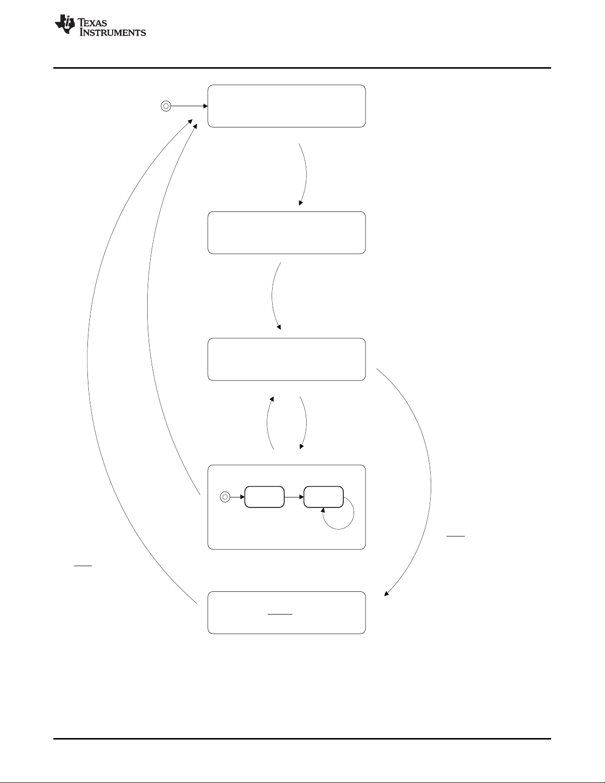
2.3 2nd Level Protection Features
The bq20z60-R1/bq20z65-R1 provides features that can be used to indicate a more serious fault via the
SAFE output. This output can be used to blow an in-line fuse to permanently disable the battery pack from
charge or discharge activity.
If any PF Threshold condition is met, the appropriate PFAlert flag is set. If the PF Threshold condition is
cleared within the PF time limit, the appropriate PFAlert flag is cleared. But if the PF Threshold condition
continues over the PF Time Limit, then the bq20z60-R1/bq20z65-R1 goes into a permanent failure
condition and the PFStatus flag is set, ad the PFlert flag is cleared.
When any NEW cause of a permanent failure is set in PFStatus function, the NEW cause is added to
Saved PF Flags 1..2. This allows Saved PF Flags 1..2 to show ALL permanent failure conditions that
have occurred.
On the first occasion of a permanent failure indicated by PFStatus or PFStatus2 change from 0x00, the
PFStatus and PFStatus2 value is stored in Saved 1st PF Flags 1..2.
SLUU386–January 2010 Detailed Description
Submit Documentation Feedback
Copyright © 2010, Texas Instruments Incorporated
21
Page 22
NoPF
PF Alert
PFCondition
CHG, DSG, ZVCHGFET turns off.
[TCA] flag set, [TDA] flag set.
Data Flash Access Read-Only.
ChargingCurrent =0
ChargingVoltage =0
Ifbit in Permanent Fail Cfg or
is set,Permanent Fail Cfg2
drive SAFEpin high and [PF] flag in
or is setSafetyStatus SafetyStatus2
MonitoredValue ≥ PFThreshold
(MonitoredValue ≥ PFThreshold
AND Timer ≥ PFTimeLimit)
OR
(AFE_Fail_Counter ≥ MaxErrorLimit )
PFKey to ManufacturerAccess
Stop and Reset Timer
Start
Timer
Wait
MonitoredValue
≥ PFThreshold
MonitoredValue < PFThreshold OR
AFE_Fail_Counter = 0
Start
AFE
Timer
Decrement
AFE_Fail_
Counter
AFE Timer
≥ AFEFail
RecoveryTime
2nd Level Protection Features
www.ti.com
2.3.1 2nd Level (Permanent) Failure Actions
When the PFStatus or PFStatus2 register changes from 0x00 to indicate a permanent failure, then the
22
following actions are taken in sequence.
• CHG, DSG, and ZVCHG FETs are turned OFF.
• The [TCA] and [TDA] flags in BatteryStatus are set.
• Data flash write access is then disabled, but the data flash can be read.
• ChargingCurrent and ChargingVoltage are set to 0.
• The appropriate bit in Saved PF Flags 1 or Saved PF Flags 2 is set.
• If the appropriate bit in Permanent Fail Cfg is set, then 0x3672 is programmed to Fuse Flag, and the
SAFE pin is driven and latched high. The [PF] flag in SafetyStatus is also set.
Related Variables:
• DF:Configuration:Registers(64):Permanent Fail Cfg 1(6), Permanent Fail Cfg 2(8)
• DF:PF Status:Device Status Data(96):Saved PF Flags 1(0), Saved PF Flags 2(2)
• DF:PF Status:Device Status Data(96):Fuse Flag(2)
• DF:PF Status:Device Status Data(96):Saved 1st PF Flags 1(32), Saved 1st PF Flags 2(34)
• SBS:ChargingCurrent(0x14)
• SBS:ChargingVoltage(0x15)
• SBS:BatteryStatus(0x16)[TCA],[TDA]
Detailed Description SLUU386–January 2010
Figure 2-5. 2nd Level Protection
Copyright © 2010, Texas Instruments Incorporated
Submit Documentation Feedback
Page 23

www.ti.com
• SBS:SafetyStatus(0x51)[PF]
• SBS:PFStatus(0x53)
2.3.2 Time-Limit-Based Protection
The bq20z60-R1/bq20z65-R1 reports a 2nd level protection alert by setting the appropriate flag in the
PFAlert or PFAlert2 register if the monitored value goes beyond the Protection Threshold. If the monitored
value stays beyond the Protection Threshold over the Max Alert duration, the bq20z60-R1/bq20z65-R1
reports a 2nd level permanent failure, clears the appropriate PFAlert flag, and sets the appropriate
PFStatus flag. See Table 2-7 for all Protection Thresholds and Max Alert durations.
Safety Overvoltage Protection— The bq20z60-R1/bq20z65-R1 monitors the individual cell voltages for
extreme values.
Safety Undervoltage Protection— The bq20z60-R1/bq20z65-R1 monitors the individual cell voltages for
extreme undervoltage values. Additionally, the bq20z60-R1/bq20z65-R1 can check cell voltages
upon wakeup from shutdown mode while the charge and precharge FETs are turned off (to detect
copper deposition).
Cell Imbalance Fault— Two methods of cell imbalance detection are implemented to provide CIM
detection both while charging and at rest. Two safety CIM flags are used, one for each detection
methods. CIM_A reflects faults detected using the active CIM detection and CIM_R reflects faults
detected using the at rest CIM detection. These flags and the bits associated with them are shown
in Table 2-7.
2nd Level Protection Features
At Rest Detection
The at rest detection mechanism starts detection if all of following conditions are reached:
• Any (CellVoltage4..1) > Rest CIM Check Voltage
• |Current| ≤ Rest CIM Current for CIM Battery Rest Time
The bq20z60-R1/bq20z65-R1 sets [CIM_R] in PFAlert if the following condition is met:
• Max difference between any (CellVoltage4..1) > Rest CIM Fail Voltage
If the above condition remains active for more than Rest CIM Time, the device goes into
permanent fail condition and moves [CIM_R] from PFAlert to PFStatus. Set Rest CIM Time to 0 to
disable this CIM detection.
Active Detection
The active detection method during charging is activated when the following conditions are met:
• Any (CellVoltage4..1) > Active CIM Check Voltage
• Current ≥ Charge Threshold Current
The bq20z60-R1/bq20z65-R1 sets [CIM_A] in PFAlert2 if the following condition is met:
• Max difference between any (CellVoltage4..1) > Active CIM Fail Voltage
If above condition remains active for more than Active CIM Time, the bq20z60-R1/bq20z65-R1
goes into permanent fail condition and moves [CIM_A] from PFAlert2 to PFStatus2. Set Active CIM
Time to 0 to disable this CIM detection.
2nd Level Protection IC Input— The PFIN input of the bq20z60-R1/bq20z65-R1 can be used to
determine the state of an external protection device such as the bq294xx. The
bq20z60-R1/bq20z65-R1 watches for the PFIN pin being driven low by an external device.
Safety Overcurrent Protection— The bq20z60-R1/bq20z65-R1 monitors the current during charging and
discharging. The overcurrent thresholds and time limits can be set independently for charging and
discharging.
Safety Overtemperature Protection— The bq20z60-R1/bq20z65-R1 monitors the pack temperature
during charging and discharging. The overtemperature thresholds and time limits can be set
independently for charging and discharging. Additionally, the two temperature sensors (TS1 and
TS2) have separate alarms, thresholds, and time limits.
SLUU386–January 2010 Detailed Description
Submit Documentation Feedback
Copyright © 2010, Texas Instruments Incorporated
23
Page 24

2nd Level Protection Features
Open Thermistor— The bq20z60-R1/bq20z65-R1 monitors the thermistor temperature readings and can
detect open thermistors by their unusually low readings. Two separate safety flags are used one for
each thermistor.
Charge and Zero-Volt Charge FET Fault Protection— The bq20z60-R1/bq20z65-R1 monitors if there
is, at any time, an attempt to turn off the CHG FET or ZVCHG FET or if the CHG bit in the AFE
OUTPUT register is set and the current still continues to flow.
Discharge FET Fault Protection— The bq20z60-R1/bq20z65-R1 monitors if there is, at any time, an
attempt to turn off the DSG FET or if the DSG bit in the AFE OUTPUT register is set and the
current still continues to flow.
Fuse State Detection— The bq20z60-R1/bq20z65-R1 can detect if an attempt has been made to blow
the fuse, but the attempt has failed. The bq20z60-R1/bq20z65-R1 monitors if the Fuse Flag is set
to 0x3672 and current is still flowing.
Protection Conditions Monitored Value PF Threshold PF Time Limit PFStatus Fail Cfg
Safety overvoltage – Voltage LT SOV Threshold, or SOV Time [SOV] [XSOV]
Safety undervoltage – Voltage SUV Threshold SUV Time [SUV] [XSUV]
Cell imbalance fault Max difference Rest CIM Fail Voltage Rest CIM Time [CIM_R] [XCIM_R]
(at rest) Any
Cell imbalance fault Max difference Active CIM Fail Active CIM Time [CIM_A] [XCIM_A]
(active) Any Voltage
2nd level protection – PFIN pin PFIN pin low PFIN Detect Time [PFIN] [XPFIN]
IC input
Safety overcurrent Current> 0 Current SOC Chg SOC Chg Time [SOCC] [XSOCC]
charge
Safety overcurrent Current< 0 Current SOC Dsg SOC Dsg Time [SOCD] [XSOCD]
discharge
Safety Current > 0 TS1Temperature SOT1 Chg Threshold SOT1 Chg Time [SOT1C] [XSOT1C]
overtemperature chg
Safety Current < 0 TS1Temperature SOT1 Dsg Threshold SOT1 Dsg Time [SOT1D] [XSOT1D]
overtemperature dsg
Open thermistor 1 – TS1Temperature Open Thermistor Open Time [SOPT1] [XSOPT1]
Open thermistor 2 – TS2Temperature Open Thermistor Open Time [SOPT2] [XSOPT2]
Charge and zero-volt (CHG FET or ZVCHG Current FET Fail Limit FET Fail Time [CFETF] [XCFETF]
charge FET fault FET turn off attempt or
CHG Flag in AFE
OUTPUT register set)
and Current > 0
Discharge FET fault (DSG FET turn off (–)Current FET Fail Limit FET Fail Time [DFETF] [XDFETF]
attempt or DSG Flag in
AFE OUTPUT register
set) and Current < 0
Fuse state Fuse Flag = 0x3672 |Current| Fuse Fail Limit Fuse Fail Time [FBF] [XFBF]
Table 2-7. Time-Limit-Based 2ndLevel Protection
• Any
(CellVoltage4..1)
> Rest CIM
Check Voltage
• |Current| ≤ Rest
CIM Current for
CIM Battery
Rest Time
• Any
(CellVoltage4..1)
> Active CIM
Check Voltage
• |Current| ≥
Charge
Detection
Current
www.ti.com
PFAlert Flag, Permanent
Flag Flag
ST SOV Threshold, or
HT SOV Threshold
CellVoltage4..1
CellVoltage4..1
TS2Temperature SOT2 Chg Threshold SOT2 Chg Time [SOT2C] [XSOT2C]
TS2Temperature SOT2 Dsg Threshold SOT2 Dsg Time [SOT2D] [XSOT2D]
24
Detailed Description SLUU386–January 2010
Submit Documentation Feedback
Copyright © 2010, Texas Instruments Incorporated
Page 25

www.ti.com
Related Variables:
• DF:2nd Level Safety:Voltage(16): LT SOV Threshold(0)
• DF:2nd Level Safety:Voltage(16): ST SOV Threshold(2)
• DF:2nd Level Safety:Voltage(16): HT SOV Threshold(4)
• DF:2nd Level Safety:Voltage(16): SOV Time(6)
• DF:2nd Level Safety:Voltage(16):SUV Threshold(7)
• DF:2nd Level Safety:Voltage(16):SUV Time(9)
• DF:2nd Level Safety:Voltage(16):Rest CIM Current(12)
• DF:2nd Level Safety:Voltage(16):Rest CIM Fail Voltage(13)
• DF:2nd Level Safety:Voltage(16):Rest CIM Time(15)
• DF:2nd Level Safety:Voltage(16):CIM Battery Rest Time(16)
• DF:2nd Level Safety:Voltage(16): Rest CIM Check Voltage(18)
• DF:2nd Level Safety:Voltage(16): Active CIM Fail Voltage(20)
• DF:2nd Level Safety:Voltage(16): Active CIM Time(22)
• DF:2nd Level Safety:Voltage(16): Active CIM Check Voltage(23)
• DF:2nd Level Safety:Voltage(16):PFIN Detect Time(25)
• DF:2nd Level Safety:Current(17):SOC Chg(0)
• DF:2nd Level Safety:Current(17):SOC Chg Time(2)
• DF:2nd Level Safety:Current(17):SOC Dsg(3)
• DF:2nd Level Safety:Current(17):SOC Dsg Time(5)
• DF:2nd Level Safety:Temperature(18):SOT1 Chg Threshold(0)
• DF:2nd Level Safety:Temperature(18):SOT1 Chg Time(2)
• DF:2nd Level Safety:Temperature(18):SOT2 Chg Threshold(3)
• DF:2nd Level Safety:Temperature(18):SOT2 Chg Time(5)
• DF:2nd Level Safety:Temperature(18):SOT1 Dsg Threshold(6)
• DF:2nd Level Safety:Temperature(18):SOT1 Dsg Time(8)
• DF:2nd Level Safety:Temperature(18):SOT2 Dsg Threshold(9)
• DF:2nd Level Safety:Temperature(18):SOT2 Dsg Time(11)
• DF:2nd Level Safety:Temperature(18):Open Thermistor(12)
• DF:2nd Level Safety:Temperature(18):Open Time(14)
• DF:2nd Level Safety:FET Verification(19):FET Fail Limit(0)
• DF:2nd Level Safety:FET Verification(19):FET Fail Time(2)
• DF:2nd Level Safety:Fuse Verification(21):Fuse Fail Limit(0)
• DF:2nd Level Safety:Fuse Verification(21):Fuse Fail Time(2)
• DF:Configuration:Registers(64):Permanent Fail Cfg 1(6), Permanent Fail Cfg 2(8)
• DF:PF Status:Device Status Data(96):Saved PF Flags 1(0), Saved PF Flags 2(2)
• SBS:TS1Temperature(0x5e)
• SBS:TS2Temperature(0x5f)
• SBS:Voltage(0x09)
• SBS:Current(0x0a)
• SBS:CellVoltage4..1(0x3c..0x3f)
• SBS:PFStatus(0x53)
2nd Level Protection Features
2.3.3 Limit-Based Protection
The bq20z60-R1/bq20z65-R1 reports a 2nd level permanent failure and sets the appropriate PFStatus flag
if the internal error counter reaches the maximum error limit. The internal error counter is incremented by
one if the error happens and reset to zero (0) for every good communication cycle.
SLUU386–January 2010 Detailed Description
Submit Documentation Feedback
Copyright © 2010, Texas Instruments Incorporated
25
Page 26

2nd Level Protection Features
AFE Communication Fault Protection— The gas gauge in the bq20z60-R1/bq20z65-R1 periodically
validates its read and write communications with the AFE. If either a read or write verify fails, an
internal AFE_Fail_Counter is incremented. If the AFE_Fail_Counter reaches AFE Fail Limit, the
bq20z60-R1/bq20z65-R1 reports an [AFE_C] permanent failure. The AFE_Fail_Counter is reset to
zero (0) for every good communication cycle. If the AFE Fail Limit is set to 0, this feature is
disabled. An [AFE_C] fault can also be declared if, after a full reset, the initial gain and offset values
read from the AFE cannot be verified. These values are A/D readings of the AFE VCELL output.
The AFE offset values are verified by reading the values twice and confirming that the readings are
within acceptable limits. The maximum difference between two readings is set with AFE Init Limit.
The maximum number of read retries, if offset and gain value verification fails and an [AFE_C] fault
is declared, is set in AFE Fail Limit.
Periodic AFE Verification— The gas gauge in the bq20z60-R1/bq20z65-R1 periodically
(AFE Check Time) compares certain RAM content of the AFE with that of the data flash and the
expected control-bit states. This function is disabled if AFE Check Time is set to 0. If an error is
detected, the internal AFE_Fail_Counter is incremented. If the internal AFE_Fail_Counter reaches
the AFE Fail Limit, the bq20z60-R1/bq20z65-R1 reports a permanent failure.
AFE Init Verification— After a full reset, the bq20z60-R1/bq20z65-R1 gas gauge and the AFE offset and
gain values are read twice and compared. The AFE Init Limit sets the maximum difference in A/D
counts of two successful readings of offset and gain, which the bq20z60-R1/bq20z65-R1 still
considers as the same value. If the gain and offset values are still not considered the same after
AFE Init Retry Limit comparison retries, the bq20z60-R1/bq20z65-R1 reports a permanent failure
error.
Data Flash Failure— The bq20z60-R1/bq20z65-R1 can detect if the data flash is not operating correctly.
A permanent failure is reported when either: (i) After a full reset the instruction flash checksum does
not verify; (ii) if any data flash write does not verify; or (iii) if any data flash erase does not verify.
www.ti.com
Table 2-8. Error-Based 2nd Level Protection
Protection Monitored Value Fail Recovery
AFE Periodic communication AFE_Fail_Counter is reset to AFE Fail Limit [AFE_C] [XAFE_C]
communication with the AFE zero (0) per each
fault AFE Fail Recovery Time period
Periodic AFE Check RAM of the AFE with Decrement of internal AFE Fail Limit [AFE_P] [XAFE_P]
verification AFE Check Time period AFE_Fail_Counter by one per
AFE Fail Recovery Time
period.
AFE initialization Initial gain and offset values – AFE Init Retry Limit [AFE_C] [XAFE_C]
from the AFE after full reset
Data flash failure Data flash – Falseflash checksum after [DFF] [XDFF]
Max Error Limit (Set to 0 PFAlert Flag, Permanent Fail
to Disable Protection) PFStatus Flag Cfg Flag
reset, data flash write not
verified, data flash erase
not verified
Related Variables:
• DF:2nd Level Safety:FET Verification(19):FET Fail Limit(0)
• DF:2nd Level Safety:FET Verification(19):FET Fail Time(2)
• DF:2nd Level Safety:AFE Verification(20):AFE Check Time(0)
• DF:2nd Level Safety:AFE Verification(20):AFE Fail Limit(1)
• DF:2nd Level Safety:AFE Verification(20):AFE Fail Recovery Time(2)
• DF:2nd Level Safety:AFE Verification(20):AFE Init Retry Limit(3)
• DF:2nd Level Safety:AFE Verification(20):AFE Init Limit (4)
• DF:Configuration:Registers(64):Permanent Fail Cfg(6)
• DF:PF Status:Device Status Data(96):Saved PF Flags 1(0)
• SBS:PFStatus(0x53)
26
Detailed Description SLUU386–January 2010
Submit Documentation Feedback
Copyright © 2010, Texas Instruments Incorporated
Page 27

www.ti.com
2.3.4 Clearing Permanent Failure
A bq20z60-R1/bq20z65-R1 permanent failure can be cleared by sending two ManufacturerAccess
commands in sequence: the first word of the PFKey followed by the second word of the PFKey. After
sending these two commands in sequence, PFStatus flags are cleared. Refer to Permanent Fail Clear
(PFKey) Manufacturer access for further details.
Related Variables:
• SBS:ManufacturerAccess(0x00)
• SBS:PFStatus(0x53)
2.4 Gas Gauging
The bq20z60-R1/bq20z65-R1 features Impedance Track™ (IT) gauging algorithm and is capable of
supporting a maximum battery pack capacity of 32Ah. The gas gauge measures individual cell voltages,
pack voltage, temperature, and current using features of the AFE. The bq20z60-R1/bq20z65-R1
determines battery state of charge by analyzing individual cell voltages when a time exceeding 35 minutes
has passed since the last charge or discharge activity of the battery. The bq20z60-R1/bq20z65-R1
measures charge and discharge activity by monitoring the voltage across a small-value series sense
resistor (10 mΩ typ.) between the cell stack negative terminal and the negative terminal of the battery
pack. The battery state of charge is subsequently adjusted during load or charger application using the
integrated charge passed through the battery.
2.4.1 Impedance Track Configuration
Load Mode— During normal operation, the battery-impedance profile compensation of the Impedance
Track algorithm can provide more-accurate full-charge and remaining state-of-charge information if
the typical load type is known. The two selectable options are constant current (Load Mode = 0)
and constant power (Load Mode = 1).
Gas Gauging
Load Select— In order to compensate for the I × R drop near the end of discharge, the
bq20z60-R1/bq20z65-R1 must be configured for whatever current (or power) will flow in the future.
While it cannot be exactly known, the bq20z60-R1/bq20z65-R1 can use load history such as the
average current of the present discharge to make a sufficiently accurate prediction. The
bq20z60-R1/bq20z65-R1 can be configured to use several methods of this prediction by setting the
Load Select value. Because this estimate has only a second-order effect on remaining capacity
accuracy, different measurement-based methods (0 to 3, and method 7) result in only minor
differences in accuracy. However, methods 4 to 6, where an estimate is arbitrarily assigned by the
user, can result in significant error if a fixed estimate is far from the actual load. For highly variable
loads, selection 7 will give the most conservative estimate and is preferable.
Constant Current (Load Mode = 0) Constant Power (Load Mode = 1)
0 = Avg I Last Run Avg P Last Run
1 = Present average discharge current Present average discharge power
2 = Current Current × Voltage
3 = AverageCurrent (default) AverageCurrent × average Voltage
4 = Design Capacity / 5 Design Energy / 5
5 = AtRate (mA) AtRate (10 mW)
6 = User Rate-mA User Rate-mW
7= Max Avg I Last Run Max Avg P Last Run
Pulsed Load Compensation and Termination Voltage— In order to take into account pulsed loads
while calculating remaining capacity until Term Voltage threshold is reached, the
bq20z60-R1/bq20z65-R1 monitors not only average load but also short load spikes. The maximum
voltage deviation during a load spike is continuously updated during discharge and stored in
Delta Voltage.
SLUU386–January 2010 Detailed Description
Submit Documentation Feedback
Copyright © 2010, Texas Instruments Incorporated
27
Page 28

Gas Gauging
Reserve Battery Capacity— The bq20z60-R1/bq20z65-R1 allows an amount of capacity to be reserved
Related Variables:
• DF:SBS Configuration:Data(48):Design Capacity(22)
• DF:SBS Configuration:Data(48):Design Energy(24)
• DF:Configuration:Operation Cfg B(2)[RESCAP]
• DF:Gas Gauging:IT Cfg(80):Load Select(0)
• DF:Gas Gauging:IT Cfg(80):Load Mode(1)
• DF:Gas Gauging:IT Cfg(80):Term Voltage(59)
• DF:Gas Gauging:IT Cfg(80):User Rate-mA(76)
• DF:Gas Gauging:IT Cfg(80):User Rate-mW(78)
• DF:Gas Gauging:IT Cfg(80):Reserve Cap-mAh(80)
• DF:Gas Gauging:IT Cfg(80):Reserve Cap-mWh(82)
• DF:Gas Gauging:State(82):Avg I Last Run(21)
• DF:Gas Gauging:State(82):Avg P Last Run(23)
• DF:Gas Gauging:State(82):Delta Voltage(25)
• DF:Gas Gauging:State(82):Max I Last Run(31)
• DF:Gas Gauging:State(82):Max P Last Run(33)
• SBS:BatteryMode(0x03)[CapM]
• SBS:Voltage(0x09)
• SBS:Current(0x0a)
• SBS:AverageCurrent(0x0b)
• SBS:OperationStatus(0x54)[LDMD]
www.ti.com
in either mAh (Reserve Cap-mAh, Load Mode = 0) or 10 mWh (Reserve Cap-mWh, Load Mode
= 1) units between the point where the RemainingCapacity function reports zero capacity, and the
absolute minimum pack voltage, Term Voltage. This enables a system to report zero energy, but
still have enough reserve energy to perform a controlled shutdown, or to provide an extended sleep
period for the host system.
Also, if the [RESCAP] bit is set to 0, the reserve capacity is compensated at a no-load condition.
However, if [RESCAP] bit is set to 1, then the reserve capacity is compensated at the present
discharge rate as selected by Load Select.
2.4.2 Gas Gauge Modes
Resistance updates take place only in discharge mode, while OCV and Qmax updates only take place in
relaxation mode. Entry and exit of each mode is controlled by data flash parameters in the subclass Gas
Gauging: Current Thresholds section. In relaxation mode or discharge mode, the DSG flag in
BatteryStatus is set.
In order to prevent abnormally fast resistance change, resistance change is limited to old value +- Ra Max
Delta (mOhm). Recommended setting is 15% of 4 Ra grid point value, after optimized values of Ra are
obtained from optimization cycle.
28
Detailed Description SLUU386–January 2010
Copyright © 2010, Texas Instruments Incorporated
Submit Documentation Feedback
Page 29
DischargeMode
RelaxationMode
Current < (–) DsgCurrentThreshold
Current >(–) forQuitCurrent
DsgRelaxTime
period
ChargeMode
Current
> ChgCurrentThreshold
Current
< QuitCurrent
for ChgRelaxTime
period
OCVupdate
Qmax update
[DSG]
CellImpedance update
[DSG]
Current
> ChgCurrentThreshold
Current <(–) DsgCurrentThreshold
www.ti.com
Gas Gauging
Figure 2-6. Gas Gauge Operating Modes
SLUU386–January 2010 Detailed Description
Submit Documentation Feedback
Copyright © 2010, Texas Instruments Incorporated
29
Page 30
QuitCurrent
(–)QuitCurrent
Current
Time
RelaxationMode ChargeMode DischargeModeRelaxationMode ChargeMode DischargeMode RelaxationMode
ChgRelaxTime
DsgRelaxTime
1 10 1 1 10[DSG]
Gas Gauging
Charge mode is exited and relaxation mode is entered when Current goes below Quit Current for a
period of Chg Relax Time. Discharge mode is entered when Current goes below
(–)Dsg Current Threshold. Discharge mode is exited and relaxation mode is entered when Current goes
above (–)Quit Current threshold for a period of Dsg Relax Time. Charge mode is entered when Current
goes above Chg Current Threshold.
www.ti.com
Figure 2-7. Gas Gauge Operating Mode Example
Related Variables:
• DF:Gas Gauging:Current Thresholds(81):Dsg Current Threshold(0)
• DF:Gas Gauging:Current Thresholds(81):Chg Current Threshold(2)
• DF:Gas Gauging:Current Thresholds(81):Quit Current(4)
• DF:Gas Gauging:Current Thresholds(81):Dsg Relax Time(6)
• DF:Gas Gauging:Current Thresholds(81):Chg Relax Time(7)
• SBS:Current(0x0a)
• SBS:BatteryStatus(0x16)[DSG]
• SBS:OperationStatus(0x54)[VOK],[R_DIS],[QEN]
2.4.3 Qmax
The total battery capacity is found by comparing states of charge before and after applying the load with
the amount of charge passed. When an applications load is applied, the impedance of each cell is
measured by comparing the open circuit voltage (OCV) obtained from a predefined function for present
state of charge with the measured voltage under load.
Measurements of OCV and charge integration determine chemical state of charge and Chemical Capacity
(Qmax).
30
Detailed Description SLUU386–January 2010
Copyright © 2010, Texas Instruments Incorporated
Submit Documentation Feedback
Page 31

www.ti.com
The bq20z60-R1/bq20z65-R1 acquires and updates the battery-impedance profile during normal battery
usage. It uses this profile, along with state-of-charge and the Qmax values, to determine
FullChargeCapacity and RelativeStateOfCharge specifically for the present load and temperature.
FullChargeCapacity reports a capacity or energy available from a fully charged battery reduced by
Reserve Cap-mAh or Reserve Cap-mWh under the present load and present temperature until Voltage
reaches the Term Voltage.
Related Variables:
• DF:Gas Gauging:IT Config(80):Term Voltage(59)
• SBS:Voltage(0x09)
• SBS:RelativeStateOfCharge(0x0d)
• SBS:FullChargeCapacity(0x10)
2.4.3.1 Qmax Initial Values
The initial Qmax Pack, Qmax Cell 0, Qmax Cell 1, Qmax Cell 2, and Qmax Cell 3 values should be
taken from the cell manufacturers' data sheet multiplied by the number of parallel cells, and are also used
for the DesignCapacity function value in the Design Capacity data flash value.
See the Theory and Implementation of Impedance Track Battery Fuel-Gauging Algorithm in bq20zxx
Product Family application report (SLUA364B) for further details.
Related Variables:
• DF:SBS Configuration:Data(48):Design Capacity(22)
• DF:Gas Gauging:State(82):Qmax Cell 0(0)
• DF:Gas Gauging:State(82):Qmax Cell 1(2)
• DF:Gas Gauging:State(82):Qmax Cell 2(4)
• DF:Gas Gauging:State(82):Qmax Cell 3(6)
• DF:Gas Gauging:State(82):Qmax Pack(8)
• SBS:DesignCapacity(0x18)
Gas Gauging
2.4.3.2 Qmax Update Conditions
The bq20z60-R1/bq20z65-R1 updates the no-load full capacity (QMAX) when two open circuit voltage
(OCV) readings are taken. These OCV readings are affected by the setting of [CHGOCV_DIS] and taken
when the battery is in a relaxed state before and after charge or discharge activity. A relaxed state is
achieved if the battery voltage has a dV/dt of < 4 μV/s. Typically it takes 2 hours in a charged state and 5
hours in a discharged state to ensure that the dV/dt condition is satisfied. If 5 hours. is exceeded, a
reading is taken even if the dV/dt condition was not satisfied. A QMAX update is disqualified under the
following conditions:
Temperature— If Temperature is outside of the range 10°C to 40°C.
Delta Capacity— If the capacity change between suitable battery rest periods is less than 37%.
Voltage— If CellVoltage4..1 is in the range of 3737 mV to 3800 mV for the default LION chemistry. (See
the Support of Multiple Li-Ion Chemistries With Impedance Track Gas Gauges application note
(SLUA372) for the voltage ranges of other chemistries.)
Offset Error— If offset error accumulated during time passed from previous OCV reading exceeds 1% of
Design Capacity, update is disqualified. Offset error current is calculated as CC Deadband / sense
resistor value.
Related Variables:
• DF:Calibration:Current(107):CC Deadband(2)
• SBS:Temperature(0x08)
• SBS:RelativeStateOfCharge(0x0d)
• SBS:AbsoluteStateOfCharge(0x0e)
• SBS:DesignCapacity(0x18)
SLUU386–January 2010 Detailed Description
Submit Documentation Feedback
Copyright © 2010, Texas Instruments Incorporated
31
Page 32

Charge Control
• SBS:CellVoltage4(0x3c)
• SBS:CellVoltage3(0x3d)
• SBS:CellVoltage2(0x3e)
• SBS:CellVoltage1(0x3f)
• SBS:OperationStatus(0x54)[VOK],[QEN]
Due to variations in charging voltages and taper current, chemical state of charge at the end of charge is
not always 100%. To account for the difference in state of charge achieved by different charges, the
gas-gauge learns actual depth of discharge after charge termination and relaxation for more than 30
minutes. These values are store in dataflash individually for each cell as follows:
• Cell 0 Chg DOD at EOC = 0
• Cell 1 Chg DOD at EOC = 0
• Cell 2 Chg DOD at EOC = 0
• Cell 3 Chg DOD at EOC = 0
Units of DOD are in an internal format. To convert it to %, the internal units should be divided by 163.84.
2.5 Charge Control
The bq20z60-R1/bq20z65-R1 can report to a smart charger the appropriate charging current needed for
constant-current charging and the charging voltage needed for constant-voltage charging per the charging
algorithm by using the ChargingCurrent and ChargingVoltage functions. The actual charging status of the
bq20z60-R1/bq20z65-R1 is indicated with flags and can be read out with the ChargingStatus function.
Related Variables:
• SBS:ChargingCurrent(0x14)
• SBS:ChargingVoltage(0x15)
• SBS:ChargingStatus(0x55)
www.ti.com
2.5.1 Charge Control SMBus Broadcasts
All broadcasts to a host or a smart charger are enabled by the [BCAST] bit. If the [HPE] bit is enabled,
master-mode broadcasts to the host address are PEC enabled. If the [CPE] bit is enabled, master-mode
broadcasts to the Smart-Charger address are PEC enabled. When broadcast is enabled, the following
broadcasts are sent:
• ChargingVoltage and ChargingCurrent broadcasts are sent to the Smart-Charger device address
(0x12) every 10 to 60 seconds.
• If any of the [OCA], [TCA], [OTA], [TDA], [RCA], [RTA] flags are set, the AlarmWarning broadcast is
sent to the host device address (0x14) every 10 seconds. Broadcasts stop when all flags above have
been cleared.
• If any of the [OCA], [TCA], [OTA] or [TDA] flags are set, the AlarmWarning broadcast is sent to
Smart-Charger device address every 10 seconds. Broadcasts stop when all flags above have been
cleared.
Related Variables:
• DF:Configuration:Registers(64):Operation Cfg B(2)[CPE],[HPE],[BCAST]
• SBS:ChargingCurrent(0x14)
• SBS:ChargingVoltage(0x15)
• SBS:BatteryStatus(0x16)[OCA],[TCA],[OTA],[TDA],[RCA],[RTA]
2.5.2 Cell Balancing
The bq20z60-R1/bq20z65-R1 can determine the chemical state of charge of each cell using the
Impedance Track algorithm. The cell balancing algorithm used in the bq20z60-R1/bq20z65-R1 decreases
the differences in imbalanced cells in a fully charged state gradually, which prevents fully charged cells
from becoming overcharged causing excessive degradation. This increases overall pack energy by
preventing premature charge termination. More information can be found in the Cell Balancing Using the
bq20zxx application report (SLUA340B).
32
Detailed Description SLUU386–January 2010
Submit Documentation Feedback
Copyright © 2010, Texas Instruments Incorporated
Page 33

www.ti.com
The algorithm determines the amount of charge needed to fully charge each cell. There is a bypass FET
in parallel with each cell connected to the AFE. The FET is enabled for each cell with charge greater than
the lowest charged cell to reduce charge current through those cells. Each FET is enabled for a
precalculated time as calculated by the cell balancing algorithm. When any bypass FET is turned on, then
the [CB] charging status flag is set, otherwise the [CB] flag is cleared.
Cell balancing is active after a Qmax update has occurred with the FC bit set and OCV taken. This state
can be determined by the Update Status being set to 0x0E.
If Min Cell Deviation is set to 0, cell balancing is disabled and all bypass FETs stay OFF.
The bypass time needed for each cell is calculated as:
Min Cell Deviation = R / (duty_cycle × V_avg) × 3.6 s/mAh
Where:
R = internal bypass FET resistance of 500 Ω (typ.) + 2 series input filter resistors, Rχ. For example: if
input filter Rχ value is 100 Ω, R = 500 + 2 × Rχ = 700 Ω.
V_avg = 3.6 V
duty_cycle = 0.4 typ.
Related Variables:
• DF:Charge Control:Cell Balancing Cfg(37):Min Cell Deviation(0)
• SBS:ChargingStatus(0x55)[CB]
2.5.3 Charge-Inhibit Mode
Charge Control
If the bq20z60-R1/bq20z65-R1 is in discharge mode or relaxation mode ([DSG] = 1), the
bq20z60-R1/bq20z65-R1 goes into charge-inhibit mode and sets the ChargingCurrent and
ChargingVoltage values to 0 to inhibit charging if:
• Temperature < JT1 limit OR
• Temperature > JT3 limit
In charge-inhibit mode, the [XCHG] flag in ChargingStatus is set. If the [CHGIN] bit in Operation Cfg B is
set, the CHG FET and ZVCHG FET (if used) are also turned off when the bq20z60-R1/bq20z65-R1 is in
charge-inhibit mode.
The bq20z60-R1/bq20z65-R1 allows charging to resume when:
• Temperature ≥ JT1 + Temp Hys AND
• Temperature ≤ JT3 – Temp Hys
The FETs also return to their previous states at that time. The [XCHG] flag is cleared when the foregoing
conditions are met, when a charge fault condition is detected, or when the battery is removed if in
removable mode ([NR] = 0).
SLUU386–January 2010 Detailed Description
Submit Documentation Feedback
Copyright © 2010, Texas Instruments Incorporated
33
Page 34

ChargeInhibitHigh
Charging Allowed
ChargeInhibitLow
ChargingCurrent
= 0
ChargingVoltage =0
[XCHG
]
If [CHGIN
] bit set
, CHGFET and
ZVCHGFETareturnedoff.
.
Temperature
≥
JEITA T1
+ TempHys
Temperature
< JEITA T1
ChargingCurrent =0
ChargingVoltage =0
[XCHG
]
If [CHGIN
] bit set
, CHGFET and
ZVCHGFETareturnedoff.
.
Temperature
≤
JT3 – TempHys
Temperature
> JT3
Charge Control
www.ti.com
34
Detailed Description SLUU386–January 2010
Figure 2-8. Charge Inhibit
Submit Documentation Feedback
Copyright © 2010, Texas Instruments Incorporated
Page 35

www.ti.com
Related Variables:
• DF:Charge Control:Charge Temp Cfg(32):JT1(0)
• DF:Charge Control:Charge Temp Cfg(32):JT3(6)
• DF:Charge Control:Charge Temp Cfg(32):Temp Hys(10)
• DF:Configuration:Registers(64):Operation Cfg B(2)[CHGIN],[NR]
• SBS:Temperature(0x08)
• SBS:ChargingCurrent(0x14)
• SBS:ChargingVoltage(0x15)
• SBS:BatteryStatus(0x16)[DSG]
• SBS:ChargingStatus(0x55)[XCHG]
2.5.4 Charge-Suspend Mode
The bq20z60-R1/bq20z65-R1 suspends charging when:
• Temperature < JT1, OR
• Temperature > JT4
In charge-suspend mode, the [CHGSUSP] flag in ChargingStatus is set and ChargingCurrent is set to 0.
The CHG FET and ZVCHG FET (if used) are also turned off if the [CHGSUSP] bit in the Operation Cfg B
register is set.
The bq20z60-R1/bq20z65-R1 resumes charging if:
• Temperature ≥ JT1 + Temp Hys, AND
• Temperature ≤ JT3 – Temp Hys.
On resuming, the bq20z60-R1/bq20z65-R1 clears the [CHGSUSP] status flag and sets ChargingCurrent
according to the appropriate charging mode entered, and the CHG and ZVCHG FETs (if used) return to
their previous state.
The bq20z60-R1/bq20z65-R1 also leaves the charge-suspend mode and clears the [CHGSUSP] flag
when a protection condition is detected or when the battery is removed in removable battery mode ([NR] =
0).
Charge Control
SLUU386–January 2010 Detailed Description
Submit Documentation Feedback
Copyright © 2010, Texas Instruments Incorporated
35
Page 36

ChargeSuspendHigh
Charging
ChargeSuspendLow
ChargingCurrent
= 0
[CHGSUSP
]
If [CHGSUSP
] bitin
OperationCfgB
isset
, CHGFET
+ ZVCHGFETare
turnedoff
.
Temperature
≥
JT1 + TempHys
Temperature
< JT1
ChargingCurrent
= 0
[CHGSUSP
]
If [CHGSUSP
] bitin
OperationCfgB
isset
, CHGFET
+ ZVCHGFETare
turnedoff
.
Temperature
≤
JT3 - TempHys
AverageCurrent
> ChgCurrentThreshold
Temperature
> JT4
Charge Control
www.ti.com
36
Detailed Description SLUU386–January 2010
Figure 2-9. Charge Suspend
Submit Documentation Feedback
Copyright © 2010, Texas Instruments Incorporated
Page 37

www.ti.com
Related Variables:
• DF:Charge Control:Charge Temp Cfg(32):JT1(0)
• DF:Charge Control:Charge Temp Cfg(32):JT3(6)
• DF:Charge Control:Charge Temp Cfg(32):JT4(8)
• DF:Charge Control:Charge Temp Cfg(32):Temp Hys(10)
• DF:Configuration:Registers(64):Operation Cfg B(2)[CHGSUSP],[NR]
• DF:Gas Gauging:Current Thresholds(81):Chg Current Threshold(2)
• SBS:Temperature(0x08)
• SBS:AverageCurrent(0x0b)
• SBS:ChargingCurrent(0x14)
• SBS:BatteryStatus(0x16)[DSG]
• SBS:ChargingStatus(0x55)[CHGSUSP]
2.5.5 Charging and Temperature Ranges
The bq20z60-R1/bq20z65-R1 requests different charging current and charging voltage for each of the
temperature ranges defined in Section 2.1, through the ChargingVoltage and ChargingCurrent commands.
Additionally, the charging current can be set differently depending on the cell voltage. Three ranges of cell
voltage are defined using two cell voltage thresholds: Cell Voltage Threshold 1 and Cell Voltage
Threshold 2 (see Table 2-9). During charging, as cell voltage increases, ChargingCurrent is set to the
appropriate value when cell voltage crosses one of the cell voltage thresholds. However, if cell voltage
decreases below the threshold, ChargingCurrent is not set back to the previous value unless a discharge
or relax state is detected. This is done to avoid the situation where the charging current is being changed
back and forth due to the voltage drop that results from changing the charging current value.
Charge Control
Table 2-9. Cell Voltage Ranges
Condition Cell Voltage Range
max(CellVoltage4..1) < Cell Voltage Threshold 1 CVR1
Cell Voltage Threshold 1 < max(CellVoltage4..1) < Cell Voltage Threshold 2 CVR2
Cell Voltage Threshold 2 < max(CellVoltage4..1) CVR3
The dependency of the Charging Voltage and Charging Current on temperature range and cell voltage
range is summarized in Table 2-10 and illustrated in Figure 2-10 and Figure 2-11.
Table 2-10. Charging Voltage and Charging Current Dependency on Temperature Range and Cell
Voltage Range
Temp Range Cell Voltage Charging Voltage Charging Current
TR1 – 0 0
CVR1 LT Chg Current1
TR2 CVR2 LT Chg Voltage LT Chg Current2
CVR3 LT Chg Current3
CVR1 ST1 Chg Current1
TR2A CVR2 ST1 Chg Voltage ST1 Chg Current2
CVR3 ST1 Chg Current3
CVR1 ST2 Chg Current1
TR3 CVR2 ST2 Chg Voltage ST2 Chg Current2
CVR3 ST2 Chg Current3
CVR1 HT Chg Current1
TR4 CVR2 HT Chg Voltage HT Chg Current2
CVR3 HT Chg Current3
TR5 – 0 0
SLUU386–January 2010 Detailed Description
Submit Documentation Feedback
Copyright © 2010, Texas Instruments Incorporated
37
Page 38

T2 T2a T3 T4
ChgInhibit ChgInhibit
ChgSuspend
TR5
LoTempChg
TR 2
StdTempChg 1
TR2A
StdTempChg2
TR 3
HiTempChg
TR 4
T1
ChgSuspend
TR 1
LTChgVoltage
HTChgVoltage
ST 1 ChgVoltage
ST 2 ChgVoltage
Charge Control
www.ti.com
Figure 2-10. Temp Ranges and Charge Voltage for JEITA With Enhancements for More Complex
Charging Profiles
38
Detailed Description SLUU386–January 2010
Copyright © 2010, Texas Instruments Incorporated
Submit Documentation Feedback
Page 39

T2 T2a T3 T4
ChgInhibit ChgInhibit
ChgSuspend
TR 5
LoTempChg
TR 2
StdTempChg1
TR 2A
StdTempChg2
TR 3
HiTempChg
TR 4
T1
ChgSuspend
TR 1
CellVoltage
Threshold 2
CellVoltage
Threshold 1
CVR1
CVR2
CVR3
LTChgCurrent 1
LTChgCurrent 2
LTChgCurrent 3
ST1 ChgCurrent 1
ST1 ChgCurrent 2
ST1 ChgCurrent 3
ST2 ChgCurrent 1
ST2 ChgCurrent 2
ST2 ChgCurrent 3
HTChgCurrent 1
HTChgCurrent 2
HTChgCurrent 3
COVThreshold
Pre-chgVoltage
Threshold
CellVoltage
www.ti.com
Charge Control
Figure 2-11. Temp Ranges and Charge Current for JEITA With Enhancements for More Complex
2.5.5.1 Low Temperature Charging
The bq20z60-R1/bq20z65-R1 enters this mode when the Temperature function reports a temperature in
the TR2 range (JT1 < Temperature < JT2). In this mode [LTCHG] flag in ChargingStatus is set, the
ChargingVoltage is set to LT Chg Voltage, and the ChargingCurrent is set to LT Chg Current1, LT Chg
Current2, or LT Chg Current3 depending on the active cell voltage range. The charging current dataflash
values for low temp charging should be set to low current values similar to precharge mode. The
bq20z60-R1/bq20z65-R1 leaves this mode and clears the [LTCHG] flag if the Temperature goes below
JT1 or above JT2 + Temp Hys.
Charging Profiles
2.5.5.2 Standard Temperature Charging 1
The bq20z60-R1/bq20z65-R1 enters this mode when the Temperature function reports a temperature in
the TR2A range (JT2 < Temperature < JT2a). In this mode the [ST1CHG] flag in ChargingStatus is set,
ChargingVoltage is set to ST1 Chg Voltage, and the ChargingCurrent is set to ST1 Chg Current, ST1
Chg Current 2, or ST1 Chg Current 3 depending on the active cell voltage range. The
bq20z60-R1/bq20z65-R1 leaves this mode and clears the [ST1CHG] flag if the Temperature goes below
JT2 or above JT2a.
2.5.5.3 Standard Temperature Charging 2
The bq20z60-R1/bq20z65-R1 enters this mode when the Temperature function reports a temperature in
SLUU386–January 2010 Detailed Description
Submit Documentation Feedback
Copyright © 2010, Texas Instruments Incorporated
39
Page 40

Charge Control
the TR3 range (JT2a < Temperature < JT3). In this mode the [ST2CHG] flag in ChargingStatus is set,
ChargingVoltage is set to ST2 Chg Voltage, and the ChargingCurrent is set to ST2 Chg Current 1 or
ST2 Chg Current 2 or ST2 Chg Current 3 depending on the active cell voltage. The
bq20z60-R1/bq20z65-R1 leaves this mode and clears the [ST2CHG] flag if the Temperature goes below
JT2a – Temp Hys or above JT3 .
2.5.5.4 High Temperature Charging
The bq20z60-R1/bq20z65-R1 enters this mode when the Temperature function reports a temperature in
the TR4 range (JT3 < Temperature < JT4). In this mode the [HTCHG] flag in ChargingStatus is set,
ChargingVoltage is set to HT Chg Voltage, and the ChargingCurrent is set to HT Chg Current1, HT Chg
Current2, or HT Chg Current3 depending on the active cell voltage. The bq20z60-R1/bq20z65-R1 leaves
this mode and clears the [HTCHG] flag if the Temperature goes below JT3 – Temp Hys or above JT4.
Related Variables:
• DF:Charge Control:Charge Temp Cfg(32):JT1(0)
• DF:Charge Control:Charge Temp Cfg(32):JT2(2)
• DF:Charge Control:Charge Temp Cfg(32):JT2a(4)
• DF:Charge Control:Charge Temp Cfg(32):JT3(6)
• DF:Charge Control:Charge Temp Cfg(32):JT4(8)
• DF:Charge Control:Charge Temp Cfg(32):Temp Hys(10)
• DF:Charge Control:Charge Cfg(34):LT Charge Voltage(0)
• DF:Charge Control:Charge Cfg(34):LT Charge Current 1(2)
• DF:Charge Control:Charge Cfg(34):LT Charge Current 2(4)
• DF:Charge Control:Charge Cfg(34):LT Charge Current 3(6)
• DF:Charge Control:Charge Cfg(34):ST1 Charge Voltage(8)
• DF:Charge Control:Charge Cfg(34):ST1 Charge Current 1(10)
• DF:Charge Control:Charge Cfg(34):ST1 Charge Current 2(12)
• DF:Charge Control:Charge Cfg(34):ST1 Charge Current 3(14)
• DF:Charge Control:Charge Cfg(34):ST2 Charge Voltage(16)
• DF:Charge Control:Charge Cfg(34):ST2 Charge Current 1(18)
• DF:Charge Control:Charge Cfg(34):ST2 Charge Current 2(20)
• DF:Charge Control:Charge Cfg(34):ST2 Charge Current 3(22)
• DF:Charge Control:Charge Cfg(34):HT Charge Voltage(24)
• DF:Charge Control:Charge Cfg(34):HT Charge Current 1(26)
• DF:Charge Control:Charge Cfg(34):HT Charge Current 2(28)
• DF:Charge Control:Charge Cfg(34):HT Charge Current 3(30)
• DF:Charge Control:Charge Cfg(34):Cell Voltage Threshold 1(32)
• DF:Charge Control:Charge Cfg(34):Cell Voltage Threshold 2(34)
• SBS:Temperature(0x08)
• SBS:ChargingCurrent(0x14)
• SBS:ChargingVoltage(0x15)
• SBS:ChargingStatus(0x55)[LTCHG] , [ST1CHG] , [ST2CHG], [HTCHG]
www.ti.com
2.5.6 Precharge
The bq20z60-R1/bq20z65-R1 enters precharge mode during charging if any cell voltage goes below
Pre-chg Voltage Threshold limit or if any of the SafetyStatus flags, [CUV], [OCD], or [OCD2] is set.
Depending on the setting of the [ZVCHG1] and [ZVCHG0] bits in Operation Cfg A, different FETs can be
used in pre-charge mode.
40
Detailed Description SLUU386–January 2010
Copyright © 2010, Texas Instruments Incorporated
Submit Documentation Feedback
Page 41

www.ti.com
In precharge mode, the [PCHG] flag is set, the ChargingVoltage is set to Pre-chg Current, and
ChargingVoltage is set per the charging algorithm.
The bq20z60-R1/bq20z65-R1 leaves precharge mode and clears the [PCHG] flag if all cell voltages reach
or rise above Pre-chg Recovery Voltage. Precharge mode is also exited if charge suspend mode is
entered, any fault condition is detected, or the pack is removed in removable mode.
Related Variables:
• DF:Charge Control:Pre-Charge Cfg(33):Pre-chg Voltage Threshold(0)
• DF:Charge Control:Pre-Charge Cfg(33):Pre-chg Recovery Voltage(0)
• DF:Charge Control:Pre-Charge Cfg(33):Pre-chg Current(4)
• DF:Configuration:Registers(64):Operation Cfg A(0)[ZVCHG1],[ZVCHG0]
• SBS:ChargingCurrent(0x14)
• SBS:ChargingVoltage(0x15)
• SBS:CellVoltage4..1(0x3c..0x3f)
• SBS:SafetyStatus(0x51)[CUV],[OCD],[OCD2]
• SBS:ChargingStatus(0x55)[PCHG]
Charge Control
Table 2-11. Precharge FET
ZVCHG1 ZVCHG0 FET USED
0 0 ZVCHG FET
0 1 CHG FET
1 0 GPOD Pin (on the
AFE when used with
bq20z60)
1 1 No Action
2.5.7 Primary Charge Termination
The bq20z60-R1/bq20z65-R1 determines charge termination if:
• Average Charge Current < Taper Current during two consecutive Current Taper Window time
periods, AND
• The accumulated change in capacity must be > 0.25 mAh per period during two consecutive
Current Taper Window time periods, AND
• Taper voltage condition is met. Taper voltage condition is either cell voltage-based or pack
voltage-based depending on the bit [CELL_TAPER] in Operation Cfg C.
– [CELL_TAPER] =1: Max (CellVoltage4..1) + Taper Voltage ≥ ChargingVoltage / number of cells
– [CELL_TAPER] =0: Voltage + Taper Voltage ≥ ChargingVoltage
NOTE: To ensure proper charge termination, it is recommend that Taper Current be set to a value
greater than Quit Current.
The following parameters change the behavior of bq20z60-R1/bq20z65-R1 on charge termination:
Table 2-12. Primary Charge Termination
Parameter Behavior on Primary Charge Termination
[TCA Set %] = –1 [TCA] flag set, [MCHG] flag set, ChargingCurrent = Maintenance Current
[FC Set %] = –1 [FC] flag set
[CHGFET] set CHG FET turned off
[CSYNC] set RemainingCapacity = FullChargeCapacity regardless of TCA Set % value
[RSOCL] set If the [RSOCL] bit in Operation Cfg C is set then RelativeStateofCharge and RemainingCapacity are held at 99% until primary
[RSOCL] clear If the [RSOCL] bit in Operation Cfg C is cleared then RelativeStateofCharge and RemainingCapacity are not held at 99% until
charge termination occurs. Only on entering primary charge termination is 100% displayed.
primary charge termination occurs. Fractions of % greater than 99% are rounded up to display 100%.
SLUU386–January 2010 Detailed Description
Submit Documentation Feedback
Copyright © 2010, Texas Instruments Incorporated
41
Page 42

Charge Control
Related Variables:
• DF:Charge Control:Termination Cfg.(36):Maintenance Current(0)
• DF:Charge Control:Termination Cfg.(36):Taper Current(2)
• DF:Charge Control:Termination Cfg.(36):Taper Voltage(6)
• DF:Charge Control:Termination Cfg.(36):Current Taper Window(8)
• DF:Charge Control:Termination Cfg.(36):TCA Set %(9)
• DF:Charge Control:Termination Cfg.(36):FC Set %(11)
• DF:Configuration:Registers(64):Operation Cfg B(2)[CHGFET],[CSYNC]
• DF:Configuration:Registers(64):Operation Cfg C(4)[RSOCL]
• DF:Gas Gauging:Current Thresholds(81):Quit Current(4)
• SBS:Voltage(0x09)
• SBS:Current(0x0a)
• SBS:RemainingCapacity(0x0f)
• SBS:FullChargeCapacity(0x10)
• SBS:ChargingCurrent(0x14)
• SBS:BatteryStatus(0x16)[TCA],[FC]
• SBS:CellVoltage4..1(0x3c..0x3f)
• SBS:ChargingStatus(0x55)[MCHG]
2.5.8 Charging Faults
www.ti.com
The bq20z60-R1/bq20z65-R1 can report charging faults in the ChargingStatus register. When the
[OCHGI] bit in Charge Fault Cfg is set, the CHG FET is turned OFF and the ZVCHG FET is turned ON if
the [ZVCHG1], [ZVCHG0] bits in Operation Cfg A are set appropriately. If the ZVCHG FET is not used
the CHG FET remains ON, regardless of the bits set in Charge Fault Cfg, because it acts as the ZVCHG
FET.
On occurrence of a charging fault, the bq20z60-R1/bq20z65-R1:
• Sets the appropriate ChargingStatus flag
• Turns off the CHG FET, and turns on the ZVCHG FET (if used) if the flag in Charge Fault Cfg and
ChargingStatus matches. The DSG FET is also turned off if charging fault is a Battery Depleted fault.
• Sets the ChargingCurrent = 0, ChargingVoltage = 0; (ChargingVoltage is not set to zero if it is a
Battery Depleted fault).
• Sets the [TCA] flag in BatteryStatus
• Sets the [OCA] flag in BatteryStatus if it is an Overcharge fault
On recovery, the bq20z60-R1/bq20z65-R1:
• Resets the appropriate ChargingStatus flags
• Sets the CHG FET and ZVCHG FET (if used) to previous states. (DSG FET is also allowed to turn on
again on recovery from Battery Depleted fault).
• Sets ChargingCurrent and ChargingVoltage back to previous state according to charging algorithm.
• Resets [TCA] (and [OCA] if it was set) flag in BatteryStatus
Precharge Mode Timeout
When Current ≥ Chg Current Threshold, the bq20z60-R1/bq20z65-R1 starts the Precharge Timer. The
Precharge Timer is suspended when precharge mode is not active ([PCHG] = 0). Set Precharge Timeout
[PCMTO] to zero to disable this feature.
The bq20z60-R1/bq20z65-R1 goes into precharge mode charging timeout [PCMTO] if:
• Precharge timer ≥ Precharge Timeout
The bq20z60-R1/bq20z65-R1 recovers if:
• Current ≤ (–)Dsg Current Threshold, OR
• Pack is removed and reinserted, if [NR] = 0
Charge Mode Timeout
42
Detailed Description SLUU386–January 2010
Submit Documentation Feedback
Copyright © 2010, Texas Instruments Incorporated
Page 43

www.ti.com
When Current is ≥ Chg Current Threshold, the bq20z60-R1/bq20z65-R1 starts the Charge Timer. The
Charge Timer is suspended when charge is not active ([LTCHG] = 0, [ST1CHG] = 0, [ST2CHG] = 0, and
[HTCHG] = 0 , or when [DSG] = 1. The Charge Timer is reset when an amount of discharge greater than
Over Charge Recovery is detected or if the pack is removed and reinserted when [NR] = 0. Set Charge
Timeout to 0 to disable this feature.
The bq20z60-R1/bq20z65-R1 goes into charge mode charging timeout if:
• Charge timer ≥ Charge Timeout
The bq20z60-R1/bq20z65-R1 recovers if:
• Current ≤ (–)Dsg Current Threshold OR
• Pack is removed and reinserted if [NR] = 0
Overcharging Voltage
The bq20z60-R1/bq20z65-R1 goes into overcharging voltage mode if:
• Voltage ≥ ST2 Chg Voltage + Over Charging Voltage for minimum Over Charging Volt Time period.
The bq20z60-R1/bq20z65-R1 recovers, if:
• Voltage ≤ ST2 Chg Voltage
Overcharging Current
The bq20z60-R1/bq20z65-R1 goes into overcharging current mode if:
• Current ≥ ChargingCurrent + Over Charging Current for minimum Over Charging Curr Time period.
The bq20z60-R1/bq20z65-R1 recovers, if:
• AverageCurrent ≤ Over Charging Curr Recov
Overcharge
The bq20z60-R1/bq20z65-R1 goes into overcharge mode if the battery pack is charged in excess of
FullChargeCapacity by Over Charge Capacity:
The bq20z60-R1/bq20z65-R1 recovers if any of the following conditions are met:
• Pack removed and reinserted ([NR] = 0)
• Continuous amount of discharge over Over Charge Recovery and AverageCurrent < 0,
• RemainingCapacity ≤ FC Clear %
Battery Depleted
The bq20z60-R1/bq20z65-R1 goes into battery depleted mode if:
• Voltage ≤ Depleted Voltage for Depleted Voltage Time and charger is present
The bq20z60-R1/bq20z65-R1 recovers, if:
• Voltage > Depleted Voltage Recovery
Charge Control
when [NR] = 1
Table 2-13. Charging Faults
ChargingStatus Flag,
Charge Fault Fault Condition Recovery Condition Charge Fault
Configuration Flag
Precharge Precharge Timer ≥ Precharge Timeout Current ≤ (–)Dsg Current Threshold, OR [PCMTO]
Timeout pack removed and reinserted if [NR] = 0
Charge Timeout Charge Timer ≥ Charge Timeout [CMTO]
Overcharging Voltage ≥ ST2 Chg Voltage + Voltage ≤ ST2 Chg Voltage [OCHGV]
Voltage Over Charging Voltage for minimum
Over Charging Volt Time
Overcharging Current ≥ ChargingCurrent + AverageCurrent ≤ Over Charging Curr [OCHGI]
Current Over Charging Current for minimum Over Recov
Charging Curr Time
SLUU386–January 2010 Detailed Description
Submit Documentation Feedback
Copyright © 2010, Texas Instruments Incorporated
43
Page 44

Charge Control
Charge Fault Fault Condition Recovery Condition Charge Fault
Overcharge RemainingCapacity – FullChargeCapacity ≥ Pack removed and reinserted if [NR] = 0, [OC]
Battery Depleted Voltage ≤ Depleted Voltage for minimum Voltage > Depleted Voltage Recovery [XCHGLV]
Related Variables:
• DF:Charge Control:Charge Cfg(34):ST2 Chg Voltage(16)
• DF:Charge Control:Termination Cfg.(36):FC Clear %(12)
• DF:Charge Control:Charging Faults(38):Over Charging Voltage(0)
• DF:Charge Control:Charging Faults(38):Over Charging Volt Time(2)
• DF:Charge Control:Charging Faults(38):Over Charging Current(3)
• DF:Charge Control:Charging Faults(38):Over Charging Curr Time(5)
• DF:Charge Control:Charging Faults(38):Over Charging Curr Recov(6)
• DF:Charge Control:Charging Faults(38):Depleted Voltage(8)
• DF:Charge Control:Charging Faults(38):Depleted Voltage Time(10)
• DF:Charge Control:Charging Faults(38):Depleted Recovery(11)
• DF:Charge Control:Charging Faults(38):Over Charge Capacity(13)
• DF:Charge Control:Charging Faults(38):Over Charge Recovery(15)
• DF:Charge Control:Charging Faults(38):Charge Timeout(17)
• DF:Charge Control:Charging Faults(38):Precharge Timeout(19)
• DF:Charge Control:Charging Faults(38):Charge Fault Cfg(21)
• DF:Configuration:Registers(64):Operation Cfg B(2)[NR]
• SBS:Voltage(0x09)
• SBS:Current(0x0a)
• SBS:AverageCurrent(0x0b)
• SBS:ChargingCurrent(0x14)
• SBS:BatteryStatus(0x16)[TDA],[TCA],[OCA]
• SBS:ChargingStatus(0x55)[LTCHG],[STCHG],[HTCHG]
www.ti.com
Table 2-13. Charging Faults (continued)
ChargingStatus Flag,
Configuration Flag
Over Charge Capacity OR continuous amount of discharge of
Over Charge Recovery if [NR] = 1, OR
RemainingCapacity ≤ FC Clear %
Depleted Voltage Time
44
Detailed Description SLUU386–January 2010
Submit Documentation Feedback
Copyright © 2010, Texas Instruments Incorporated
Page 45

www.ti.com
2.5.9 Discharge and Charge Alarms
The bq20z60-R1/bq20z65-R1 enables [TDA], [FD], [TCA] and [FC] flags in BatteryStatus to be set or
cleared on the following thresholds based on RelativeStateOfCharge. All thresholds can be disabled by
setting them to –1. FC Clear % should not be disabled by setting to –1.
RelativeStateOfCharge
The [TDA] and [FD] flags in BatteryStatus can also be set or cleared based on Voltage. If the voltage
settings are not used, then they should be set to extreme range values.
≤TDA Volt Threshold for a period of TDA Volt Time and
Voltage
≤FD Volt Threshold for a period of FD Volt Time [FD] is set.
Discharge-Inhibit Mode
Threshold BatteryStatus Flag
≤TDA Set % and discharging [TDA] is set.
≥TDA Clear % [TDA] is cleared.
≤FD Set % [FD] is set.
≥FD Clear % [FD] is cleared.
≥TCA Set % [TCA] is set.
≤TCA Clear % [TCA] is cleared.
≥FC Set % [FC] is set.
≤FC Clear % [FC] is cleared.
Threshold BatteryStatus Flag
discharging
≥TDA Clear Volt [TDA] is cleared.
≥FD Clear Volt [FD] is cleared.
[TDA] is set.
Related Variables:
• DF:Charge Control:Termination Cfg.(36):TCA Set %(9)
• DF:Charge Control:Termination Cfg.(36):TCA Clear %(10)
• DF:Charge Control:Termination Cfg.(36):FC Set %(11)
• DF:Charge Control:Termination Cfg.(36):FC Clear %(12)
• DF:SBS Configuration:Configuration(49):TDA Set %(0)
• DF:SBS Configuration:Configuration(49):TDA Clear %(1)
• DF:SBS Configuration:Configuration(49):FD Set %(2)
• DF:SBS Configuration:Configuration(49):FD Clear %(3)
• DF:SBS Configuration:Configuration(49):TDA Set Volt Threshold(4)
• DF:SBS Configuration:Configuration(49):TDA Set Volt Time(6)
• DF:SBS Configuration:Configuration(49):TDA Clear Volt(7)
• DF:SBS Configuration:Configuration(49):FD Set Volt Threshold(9)
• DF:SBS Configuration:Configuration(49):FD Volt Time(11)
• DF:SBS Configuration:Configuration(49):FD Clear Volt(12)
• SBS:Voltage(0x09)
• SBS:RelativeStateOfCharge(0x0d)
2.6 Discharge-Inhibit Mode
The bq20z60-R1/bq20z65-R1 prevents discharging if Temperature > Hi Dsg Start Temp. When this
happens, the bq20z60-R1/bq20z65-R1 goes into discharge inhibit mode. In discharge inhibit mode,
discharging is disabled, and [XDSG], [DSGIN] in OperationStatus and [TDA] in BatteryStatus are set. The
bq20z60-R1/bq20z65-R1 returns to normal mode and allows discharging if Temperature becomes less
than or equal Hi Dsg Start Temp.
Related Variables:
• DF:1st Level Safety:Temperature(2):Hi Dsg Start Temp(20)
• SBS:Temperature(0x08)
SLUU386–January 2010 Detailed Description
Submit Documentation Feedback
Copyright © 2010, Texas Instruments Incorporated
45
Page 46

PermanentFailureDisplay
DisplayInactive
DISP L-H Transition
AND set
AND set
AND cleared
[PFD0]
[PFD1]
[SLED]
PermanentFailureDisplayontime
> 2 × LED
HoldTime
perpermanentfailurebitset
DisplayDisabled
[CUV] reset
[CUV] set
LEDsOFF
DisplaysPermanentFailureError
Code
DischargeDisplay
LEDsshowchargelevel
ANDif
[RCA]
isset,activeLEDsare
alsoflashing.
LEDs Active
LEDsOFF
Manufacturer
Access
LEDsON
Manufacturer
Access
LEDsOFF
ChargeDisplay
LEDsshowchargelevel AND highest
chargelevelLEDisblinking
ANDif
[RCA]
isset, allactiveLEDs
areflashing.
[
]
[PFD1]
[ ]
LEDHoldTime
set AND
cleared AND
cleared AND
heldfor
SLED
DISP
PFD0
ManufacturerAccess Display
OR setANDexitfromReset
OR isset AND isset
OR H-L Transition
[LEDR]
[LEDRCA] [RCA]
DISP
LEDHoldTime
expires
DsgMode
([DSG]
= 1)
Chg Mode
( =0)[DSG]
ChargeDisplay
LEDsshowchargelevel AND highest
chargelevelLEDisblinking
ORif
[RCA]
isset,LEDsareflashing.
[CHGLED
] set AND
ChargeMode
[CHGLED] set
ANDLeave
ChargeMode
OnlyLEDsdefinedin [LED1][LED0],
areswitchedon.
LED Display
• SBS:BatteryStatus(0x16)[TDA]
• SBS:OperationStatus(0x54)[XDSG],[DCHGIN]
2.7 LED Display
2.7.1 Display Activation
www.ti.com
46
Figure 2-12. Display Activation
Detailed Description SLUU386–January 2010
Copyright © 2010, Texas Instruments Incorporated
Submit Documentation Feedback
Page 47

www.ti.com
The LED display is activated with a High to Low (H-L) transition at the DISP pin. The following flags
configure additional display activation settings. If [CUV] or [PUV] flags are set, the display is disabled.
LEDR — Set this flag to activate the display on exit from reset.
LEDRCA— Set this flag to let all active LEDs flash with LED Flash Period if [RCA] flag is set.
CHGLED— Set this flag to let the display stay activated during charging.
PFD1, PFD0— If [PFD0] is set, the permanent failure can be activated in two different ways depending on
LEDs ON, LEDs OFF, Display ON— The display can be tested with these ManufacturerAccess
Related Variables:
• DF:Configuration:Registers(64):Operation Cfg A(0)[LEDR],[LEDRCA],[CHGLED]
• DF:Configuration:Registers(64):Operation Cfg B(2)[PFD1],[PFD0]
• DF:LED Support:LED Cfg(67):LED Hold Time(6)
• SBS:ManufacturerAccess(0x00):LEDs ON(0x0032)
• SBS:ManufacturerAccess(0x00):LEDs OFF(0x0033)
• SBS:ManufacturerAccess(0x00):Display ON(0x0034)
• SBS:BatteryStatus(0x16)[RCA]
• SBS:SafetyStatus(0x51)[CUV],[PUV]
• SBS:PFStatus(0x53)
LED Display
the [PFD1] flag. If [PFD1] is cleared, the permanent failure display is active after normal capacity
display, if DISP is held low after H-L transition for LED Hold Time period. If [PFD1] is set, the
permanent failure display is activated with a H-L transition at DISP pin. The permanent failure
display stays active 2 × LED Hold Time for each flag set in PFStatus register. See "Permanent
Failure Error Codes" chapter for available error codes.
commands, LEDs ON and LEDs OFF switches all configured LEDs on or off. The Display ON
command simulates a H-L transition at the DISP pin.
2.7.2 Display Configuration
The following parameters configures the display in various ways.
DMODE— The charge level display can be configured to show either relative state of charge or absolute
state of charge.
LED1, LED0 — These bits configure the number of LEDs and the charge threshold levels used in the
LED display. The bq20z90/bq20z95 can use predefined charge levels for 3,4, or 5 LEDs or user
defined levels.
SLED — The serial LED option can be used to implement a much brighter display at the expense of
additional hardware components. With the parallel connection, the 3.3 V output from the bq29330 is
used to power the LEDs. Using that approach, current in each LED should be limited to 3 mA
maximum. With the serial option, all LEDs can be powered from the battery voltage and driven in
series through a simple constant current regulator. The current is then diverted to ground at the
various nodes between the series LEDs in order to program the desired pattern.
LED Blink Period— During charging, the top LED segment flashes with the LED Blink Period; e.g. if
battery charge is 36% and the display uses 5 LEDs, LED 2 will blink. [LEDRCA],
CHG Flash Alarm and DSG Flash Alarm will override this setting if active.
LED Flash Period— During discharge alarm, the remaining LED segments flash with LED Flash Period;
e.g. if battery charge is 36% and the display uses 5 LEDs, LED 1 and LED 2 will blink.
LED Delay— An activation delay from one LED to another LED can be set with this value.
LED Hold Time— After display activation the display will stay on LED Hold Time period. The permanent
failure display will stay on double the LED Hold Time period for each permanent failure bit set.
Related Variables:
SLUU386–January 2010 Detailed Description
Submit Documentation Feedback
Copyright © 2010, Texas Instruments Incorporated
47
Page 48

LED Display
• DF:Configuration:Registers(64):Operation Cfg A(0)[DMODE],[LED1],[LED0],[SLED],[LEDRCA]
• DF:LED Support:LED Cfg(67):LED Flash Period(0)
• DF:LED Support:LED Cfg(67):LED Blink Period(2)
• DF:LED Support:LED Cfg(67):LED Delay(4)
• DF:LED Support:LED Cfg(67):LED Hold Time(6)
• SBS:RelativeStateOfCharge(0x0d)
• SBS:AbsoluteStateOfCharge(0x0e)
2.7.3 Display Format
The bq20z60-R1/bq20z65-R1 can show state of charge using the LED display. Predefined levels for 3, 4
or 5 LEDs or user configurable levels can be selected. State of charge levels can be configured for
charging and discharging.
If the display is activated during charging the display shows the state of charge and the top LED segment
flashes at the rate of LED Blink Period (eg: if RelativeStateOfCharge = 36% and 5 LEDs are being used
then LED2 will blink). The blinking is overriden with CHG Flash Alarm or [LEDRCA]
If state of charge falls below the flash alarm level, all remaining active LEDs will flash at the
LED Flash Period. The flash alarm can be disabled by setting it to -1.
www.ti.com
48
Detailed Description SLUU386–January 2010
Copyright © 2010, Texas Instruments Incorporated
Submit Documentation Feedback
Page 49

www.ti.com
Related Variables:
• DF:Configuration:Registers(64):Operation Cfg A(0)[DMODE],[LED1],[LED0],[LEDRCA]
• DF:LED Support:LED Cfg(67):LED Flash Period(0)
• DF:LED Support:LED Cfg(67):LED Blink Period(2)
• DF:LED Support:LED Cfg(67):CHG Flash Alarm(7)
• DF:LED Support:LED Cfg(67):CHG Thresh 1(8)
• DF:LED Support:LED Cfg(67):CHG Thresh 2(9)
• DF:LED Support:LED Cfg(67):CHG Thresh 3(10)
• DF:LED Support:LED Cfg(67):CHG Thresh 4(11)
• DF:LED Support:LED Cfg(67):CHG Thresh 5(12)
• DF:LED Support:LED Cfg(67):DSG Flash Alarm(13)
• DF:LED Support:LED Cfg(67):DSG Thresh 1(14)
• DF:LED Support:LED Cfg(67):DSG Thresh 2(15)
• DF:LED Support:LED Cfg(67):DSG Thresh 3(16)
• DF:LED Support:LED Cfg(67):DSG Thresh 4(17)
• DF:LED Support:LED Cfg(67):DSG Thresh 5(18)
• SBS:RelativeStateOfCharge(0x0d)
• SBS:AbsoluteStateOfCharge(0x0e)
• SBS:BatteryStatus(0x16)[DSG]
LED Display
Table 2-14. Display Charge Level Threshold
LED1, LED0 Setting: 3 LED 4 LED 5 LED USER
Threshold Level: charge + discharge level charging level discharging level
Flash Alarm active 0% - 10% 0% - 10% 0% - 10% 0% - CHG Flash Alarm 0% - DSG Flash Alarm
LED 1 active 0% - 100% 0% - 100% 0% - 100% CHG Thresh 1 - 100% DSG Thresh 1 - 100%
LED 2 active 34% - 100% 25% - 100% 20% - 100% CHG Thresh 2 - 100% DSG Thresh 2 - 100%
LED 3 active 67% - 100% 50% - 100% 40% - 100% CHG Thresh 3 - 100% DSG Thresh 3 - 100%
LED 4 active - 75% - 100% 60% - 100% CHG Thresh 4 - 100% DSG Thresh 4 - 100%
LED 5 active - - 80% - 100% CHG Thresh 5 - 100% DSG Thresh 5 - 100%
2.7.4 Permanent Failure Error Codes
When a permanent failure occurs, the type of permanent failure error can be shown on the display. The
table below shows available error codes. The permanent failure display requires proper setting of [PFD1]
and [PFD0] bits. The permanent failure code display is disabled if [SLED] bit is set. The LED Flash Period
and LED Blink Period are fixed for these errors and not affected by the LED Data Flash settings.
PFStatus LED3 LED2 LED1
[SOPT2] Flashing with LED Flash Period Off Flashing with LED Blink Period
[SOT2D] On Off Flashing with LED Blink Period
[SOT2C] Off Off Flashing with LED Blink Period
[CIM_A] Flashing with LED Flash Period Flashing with LED Blink Period Flashing with LED Flash Period
[FBF] On Flashing with LED Blink Period Flashing with LED Flash Period
[VSHUT] Off Flashing with LED Blink Period Flashing with LED Flash Period
[SUV] Flashing with LED Flash Period Flashing with LED Blink Period On
[SOPT1] On Flashing with LED Blink Period On
[SOCD] Off Flashing with LED Blink Period On
[SOCC] Flashing with LED Flash Period Flashing with LED Blink Period Off
[AFE_P] On Flashing with LED Blink Period Off
[AFE_C] Off Flashing with LED Blink Period Off
[DFF] Flashing with LED Blink Period Flashing with LED Flash Period Flashing with LED Flash Period
SLUU386–January 2010 Detailed Description
Submit Documentation Feedback
Copyright © 2010, Texas Instruments Incorporated
49
Page 50

Device Operating Mode
PFStatus LED3 LED2 LED1
[DFETF] Flashing with LED Blink Period On Flashing with LED Flash Period
[CFETF] Flashing with LED Blink Period Off Flashing with LED Flash Period
[CIM_R] Flashing with LED Blink Period Flashing with LED Flash Period On
[SOT1D] Flashing with LED Blink Period On On
[SOT1C] Flashing with LED Blink Period Off On
[SOV] Flashing with LED Blink Period Flashing with LED Flash Period Off
[PFIN] Flashing with LED Blink Period On Off
None Flashing with LED Blink Period Off Off
Related Variables:
• DF:Configuration:Registers(64):Operation Cfg B(2)[PFD1],[PFD0]
• DF:LED Support:LED Cfg(67):LED Flash Period(0)
• DF:LED Support:LED Cfg(67):LED Blink Period(2)
2.7.5 LED Current Configuration
The sink current setting of the LED inputs to the bq20z60-R1/bq20z65-R1 can be programmed with the
following settings. All of the LEDs are programmed with the same current level.
ILED1 ILED0 Sink Current
0 0 0 mA
0 1 3 mA
1 0 4 mA
1 1 5 mA (default)
www.ti.com
Table 2-15. LED Current Configuration
Related Variables:
• DF:LED Support:LED Cfg(67):Sink Current(19)
2.8 Device Operating Mode
The bq20z60-R1/bq20z65-R1 has several device power modes. During these modes, the
bq20z60-R1/bq20z65-R1 modifies its operation to minimize power consumption from the battery.
2.8.1 Normal Mode
During normal operation, the bq20z60-R1/bq20z65-R1 takes Current, Voltage, and Temperature
measurements, performs calculations, updates SBS data, and makes protection and status decisions at
1-second intervals. Between these periods of activity, the bq20z60-R1/bq20z65-R1 is in a reduced-power
state.
PRES is sampled once per second and if PRES is high, the OperationStatus [PRES] flag is cleared. If
PRES is low, the OperationStatus [PRES] flag is set, indicating the system is present (the battery is
inserted).
If the [NR] bit is set, the PRES input can be left floating, as it is not monitored.
Related Variables:
• DF:Configuration:Registers(64):Operation Cfg B(2)[NR]
• SBS:OperationStatus(0x54)[PRES]
50
Detailed Description SLUU386–January 2010
Submit Documentation Feedback
Copyright © 2010, Texas Instruments Incorporated
Page 51

www.ti.com
2.8.2 Battery Pack Removed Mode/System Present Detection
2.8.2.1 Battery Pack Removed
The bq20z60-R1/bq20z65-R1 detects the Battery Pack Removed mode if the [NR] bit is set to 0 AND the
PRES input is high ([PRES] = 0).
On entry to the Battery Pack Removed mode, the [TCA] and [TDA] flags in BatteryStatus are set,
ChargingCurrent and ChargingVoltage are set to 0, the CHG and DSG FETs are turned off, and the
ZVCHG FET is turned off (if used).
Polling of the PRES pin continues at a rate of once every 1 s.
The bq20z60-R1/bq20z65-R1 exits the Battery Pack Removed state if the [NR] flag is set to 0 AND the
PRES input is low ([PRES] = 1). When this occurs, the [TCA] and [TDA] flags in BatteryStatus are reset.
Related Variables:
• DF:Configuration:Registers(64):Operation Cfg B(2)[NR]
• SBS:BatteryStatus(0x16)[TCA],[TDA]
• SBS:OperationStatus(0x54)[PRES]
2.8.2.2 System Present
PRES is sampled once per second, and if PRES is high, the OperationStatus [PRES] flag is cleared. If
PRES is low, the OperationStatus [PRES] flag is set, indicating the system is present (the battery is
inserted). If the [NR] bit is set, the PRES input is ignored and can be left floating.
Related Variables:
• DF:Configuration:Registers(64):Operation Cfg B(2)[NR]
• SBS:OperationStatus(0x54)[PRES]
Device Operating Mode
2.8.3 Sleep Mode
In Sleep mode, the bq20z60-R1/bq20z65-R1 measures Voltage and Temperature in Sleep Voltage Time
intervals and Current at Sleep Current Time intervals. At each interval the bq20z60-R1/bq20z65-R1
performs calculations, updates SBS data, and makes protection and status decisions. Between these
periods of activity, the bq20z60-R1/bq20z65-R1 is in a reduced-power state.
The bq20z60-R1/bq20z65-R1 enters Sleep mode when the following conditions exist:
• If the [NR] bit is set to 0, [PRES] must also be set to 0 for the bq20z60-R1/bq20z65-R1 to enter sleep.
AND one of the following conditions:
• (|Current| ≤ Sleep Current) AND (SMBus is low for Bus Low Time) AND (the [SLEEP] bit is set)
OR
• (|Current| ≤ Sleep Current) AND (ManufacturerAccess Sleep command is received) AND (the
[SLEEP] bit is set).
Entry to Sleep mode is blocked if any of the PFStatus flags is set.
On entry to sleep, if [NR] = 0, the CHG and DSG FETs are turned off, and the ZVCHG FET is turned off
(if used), regardless of the [NRCHG] setting. If [NR] = 1, the CHG FET is turned off, and the ZVCHG FET
is turned off (if used). However, if [NRCHG] is set, then the CHG FET remains on.
Also, on entry to Sleep mode, the autocalibration of the ADC begins. However, if Temperature
≤ Cal Inhibit Temp Low or Temperature ≥ Cal Inhibit Temp High, autocalibration is not started on entry
to sleep mode. The activation of autocalibration is not affected by the state of [SLEEP],
Sleep Voltage Time, Sleep Current Time, or Current.
Additionally, if sleep mode is entered in response to ManufacturerAccess Sleep command, then the ADC
autocalibration is not performed.
The bq20z60-R1/bq20z65-R1 exits Sleep mode when one or more of the following conditions exist:
• If the [NR] bit is set to 0 and [PRES] is set to 1.
SLUU386–January 2010 Detailed Description
Submit Documentation Feedback
Copyright © 2010, Texas Instruments Incorporated
51
Page 52

Device Operating Mode
• |Current| > Sleep Current
• SMBC or SMBD input transitions high
• Any current related flag is set in SafetyStatus
• [OC], [CMTO], [OCHGV], [OCHGI], and [XCHGLV] flags in ChargingStatus are set
• Wake function enabled by setting Wake Current Reg and a voltage across SRP and SRN is detected
The bq20z60-R1/bq20z65-R1 exits Sleep mode if the absolute value of Current is greater than
Sleep Current, OR the SMBC or SMBD input transitions high, OR any OperationStatus, ChargingStatus,
or SafetyStatus flags change state.
In addition, if [NR] is cleared, the bq20z60-R1/bq20z65-R1 exits Sleep mode when [PRES] = 1.
Related Variables:
• DF:Configuration:Registers(64):Operation Cfg A(0)[SLEEP]
• DF:Configuration:Registers(64):Operation Cfg B(2)[NR],[NRCHG]
• DF:Power:Power(68):Sleep Current(10)
• DF:Power:Power(68):Bus Low Time(12)
• DF:Power:Power(68):Cal Inhibit Temp Low(13)
• DF:Power:Power(68):Cal Inhibit Temp Low(15)
• DF:Power:Power(68):Sleep Voltage Time(17)
• DF:Power:Power(68):Sleep Current Time(18)
• DF:Power:Power(68):Wake Current Reg(19)
• SBS:ManufacturerAccess(0x00):Sleep(0x0011)
• SBS:Current(0x0a)
• SBS:SafetyStatus(0x51)
• SBS:OperationStatus(0x54)[PRES]
www.ti.com
2.8.4 Wake Function
The bq20z60-R1/bq20z65-R1 can exit sleep mode, if enabled, by the presence of a voltage across SRP
and SRN. The level of the current signal needed is programmed in Wake Current Reg.
Bit 7 Bit 6 Bit 5 Bit 4 Bit 3 Bit 2 Bit 1 Bit 0
Low Byte RSVD RSVD RSVD RSVD RSVD IWAKE RSNS1 RSNS0
LEGEND: RSVD = Reserved and must be programmed to 0
Figure 2-13. Wake Current Reg
IWAKE— This bit sets the current threshold for the Wake function.
0 = 0.5 A (or if RSNS0 = RSNS1 = 0, then this function is disabled)
1 = 1 A (or if RSNS0 = RSNS1 = 0, then this function is disabled)
Table 2-16. Wake Current Reg
RSNS1 RSNS0 Resistance
0 0 Disabled (default)
0 1 2.5 mΩ
1 0 5 mΩ
1 1 10 mΩ
Related Variables:
• DF:Configuration:Registers(64):Operation Cfg A(0)[SLEEP]
• DF:Power:Power(68):Wake Current Reg(19)
• SBS:Current(0x0a)
52
Detailed Description SLUU386–January 2010
Submit Documentation Feedback
Copyright © 2010, Texas Instruments Incorporated
Page 53

www.ti.com
2.8.5 Shutdown Mode
The bq20z60-R1/bq20z65-R1 enters Shutdown mode if the following conditions are met:
• [SHUTV] in Operation Cfg C is set to 0 AND Voltage ≤ Shutdown Voltage AND Current ≤ 0 for a
period of Cell Shutdown Time
OR
• [SHUTV] in Operation Cfg C is set to 1 AND Min(CellVoltage4..1) ≤ Cell Shutdown Voltage AND
Current ≤ 0 for a period of Shutdown Time
OR
• (ManufacturerAccess shutdown command received AND Current = 0) AND PackVoltage <
Charger Present threshold.
When the bq20z60-R1/bq20z65-R1 meets these conditions, the CHG, DSG, and ZVCHG FETs are turned
off, and the AFE is commanded to shut down. In Shutdown mode, the bq20z60-R1/bq20z65-R1 is
completely powered down because its supply is removed.
To exit Shutdown mode, the PACK voltage must be greater than its minimum operating voltage. When this
occurs, the AFE returns power to the bq20z60-R1/bq20z65-R1, the [WAKE] flag is set, and the AFE is
configured. The [WAKE] flag is cleared after approximately 1 s when all SBS parameters have been
measured and updated.
Related Variables:
• DF:Power:Power(68):Shutdown Voltage(2)
• DF:Power:Power(68):Shutdown Time(4)
• DF:Power:Power(68):Cell Shutdown Voltage(5)
• DF:Power:Power(68):Cell Shutdown Time(7)
• DF:Power:Power(68):Charger Present(8)
• DF:Configuration:Registers(64):Operation Cfg B(2)[NR]
• DF:Configuration:Registers(64):Operation Cfg C(4)[SHUTV]
• SBS:Voltage(0x09)
• SBS:Current(0x0a)
• SBS:CellVoltage4..1(0x3c..0x3f)
• SBS:OperationStatus(0x54)[PRES],[WAKE]
• SBS:PackVoltage(0x5a)
Security (Enables and Disables Features)
2.8.6 Ship Mode
While in sealed mode, the bq20z60-R1/bq20z65-R1 enters ship mode if ManufacturerAccess (MAC)
shutdown command (0x0010) is received 2 consecutive times AND PackVoltage < Charger Present
threshold AND no safety conditions. The 2 MAC writes cannot have any other MAC commands following
or between them. After the bq20z60-R1/bq20z65-R1 receives the 2 consecutive MAC (0x0010)
commands, the CHG, DSG, and ZVCHG FETs are turned off after Sealed Ship Delay time period. After
the passage of another Sealed Ship Delay period, ship mode is entered (i.e. after a time period which 2
times Sealed Ship Delay). For example, if Sealed Ship Delay is set to 5 seconds, then 5 seconds after
receiving the 2 MAC (0x0010) commands the FETs will turn off, and 10 seconds after receiving the 2
commands, the bq20z60-R1/bq20z65-R1 will enter ship mode.
Related Variables:
• DF:Power:Power(68):Charger Present(8)
• DF:Power:Power(68):Sealed Ship Delay(20)
• SBS:PackVoltage(0x5a)
2.9 Security (Enables and Disables Features)
There are three levels of secured operation within the bq20z60-R1/bq20z65-R1. To switch between the
levels, different operations are needed with different codes. The three levels are Sealed, Unsealed, and
Full Access.
SLUU386–January 2010 Detailed Description
Submit Documentation Feedback
Copyright © 2010, Texas Instruments Incorporated
53
Page 54

Security (Enables and Disables Features)
1. Full Access or Unsealed to Sealed— The use of the Seal Device command instructs the
bq20z60-R1/bq20z65-R1 to limit access to the SBS functions and data flash space and sets the
[SS] flag. In sealed mode, standard SBS functions have access per the Smart Battery Data
Specification, Appendix A. Extended SBS functions and data flash are not accessible. Once in
sealed mode, the part can never permanently return to Unsealed or Full Access modes.
2. Sealed to Unsealed— Instructs the bq20z60-R1/bq20z65-R1 to extend access to the SBS and data
flash space and clears the [SS] flag. In unsealed mode, all data, SBS, and DF have read/write
access. Unsealing is a two-step command performed by writing the first word of the UnSealKey to
ManufacturerAccess followed by the second word of UnSealKey to ManufacturerAccess. The
unseal key can be read and changed via the extended SBS block command UnSealKey when in
Full Access Mode. To return to the Sealed mode, either a hardware reset is needed, or the
ManufacturerAccess seal device command is needed to transit from Full Access or Unsealed to
Sealed.
3. Unsealed to Full Access— Instructs the bq20z60-R1/bq20z65-R1 to allow full access to all SBS
commands and data flash. The bq20z60-R1/bq20z65-R1 is shipped from TI in this mode. The keys
for Unsealed to Full Access can be read and changed via the extended SBS block command
FullAccessKey when in Full Access mode. Changing from Unsealed to Full Access is performed by
using the ManufacturerAccess command, by writing the first word of FullAccessKey to
ManufacturerAccess followed by the second word of the FullAccessKey to ManufacturerAccess.
The full access key can be read and changed via the extended SBS block command
FullAccessKey when in Full Access Mode. In Full Access mode, the command to go to boot ROM
can be sent.
Related Variables:
• SBS:ManufacturerAccess(0x00):Seal Device(0x0020)
• SBS:OperationStatus(0x54)[SS],[FAS]
• SBS:UnSealKey(0x60)
• SBS:FullAccessKey(0x61)
www.ti.com
54
Detailed Description SLUU386–January 2010
Submit Documentation Feedback
Copyright © 2010, Texas Instruments Incorporated
Page 55

Full AccessMode
UnsealedMode
SealedMode
NoDataFlash Access
StandardSBSCommands
DataFlashRead
/Write Access
StandardSBSCommands
SomeExtendedSBSCommands
DataFlashRead
/Write Access
StandardSBSCommands
AllExtendedSBSCommands
BootROM
Devicecanbereprogrammed
Write 0x0f00 to
ManufacturerAcces
FullHardware
ResetORwriting
0x08
toSMBus
Writelowerpartof
FullAccessKey
+ higherpartof
FullAccessKey
to
ManufacturerAccess
SealDevice
Command
SealDevice
Command
Writelowerpartof
UnsealKey
+ higherpartof
UnsealKey
to
ManufacturerAccess
www.ti.com
Security (Enables and Disables Features)
Figure 2-14. Security
SLUU386–January 2010 Detailed Description
Submit Documentation Feedback
Copyright © 2010, Texas Instruments Incorporated
55
Page 56

Calibration
2.10 Calibration
2.10.1 Coulomb-Counter Dead Band
The bq20z60-R1/bq20z65-R1 does not accumulate charge or discharge for gas gauging when the current
input is below the dead-band current threshold. The threshold is programmed in CC Deadband
(coulomb-counter dead band) and should be set sufficiently high to prevent false signal detection with no
charge or discharge flowing through the sense resistor.
Related Variable:
• DF:Calibration:Current(107):CC Deadband(1)
2.10.2 Autocalibration
The bq20z60-R1/bq20z65-R1 provides an autocalibration feature to cancel the voltage offset error across
SRP and SRN for maximum charge measurement accuracy. The bq20z60-R1/bq20z65-R1 performs
autocalibration when the SMBus lines stay low continuously for a minimum of 5 s and Temperature is
within bounds of Cal Inhibit Temp Low and Cal Inhibit Temp High.
Related Variables:
• DF:Power:Power(68):Cal Inhibit Temp Low(13)
• DF:Power:Power(68):Cal Inhibit Temp High(15)
• SBS:Temperature(0x08)
2.11 Communications
www.ti.com
The bq20z60-R1/bq20z65-R1 uses SMBus v1.1 with master mode and packet error checking (PEC)
options per the SBS specification.
2.11.1 SMBus On and Off States
The bq20z60-R1/bq20z65-R1 detects an SMBus off state when SMBC and SMBD are logic-low for ≥ 2
seconds. Clearing this state requires either SMBC or SMBD to transition high. Within 1 ms, the
communication bus is available.
2.11.2 Packet Error Checking
The bq20z60-R1/bq20z65-R1 can receive or transmit data with or without PEC.
In the write-word protocol, if the host does not support PEC, the last byte of data is followed by a stop
condition. If the host does not support PEC, the [HPE] bit should be set to 0 (default).
In the write-word protocol, the bq20z60-R1/bq20z65-R1 receives the PEC after the last byte of data from
the host. If the host does not support PEC, the last byte of data is followed by a stop condition. After
receipt of the PEC, the bq20z60-R1/bq20z65-R1 compares the value to its calculation. If the PEC is
correct, the bq20z60-R1/bq20z65-R1 responds with an ACKNOWLEDGE. If it is not correct, the
bq20z60-R1/bq20z65-R1 responds with a NOT ACKNOWLEDGE and sets an error code. If the host
supports PEC, the [HPE] bit should be set to 1.
In the read-word and block-read in master mode, the host generates an ACKNOWLEDGE after the last
byte of data sent by the bq20z60-R1/bq20z65-R1. The bq20z60-R1/bq20z65-R1 then sends the PEC, and
the host, acting as a master receiver, generates a NOT ACKNOWLEDGE and a stop condition.
Related Variable:
• DF:Configuration:Registers(64):Operation Cfg B(2)[HPE]
2.11.3 bq20z60-R1/bq20z65-R1 Slave Address
The bq20z60-R1/bq20z65-R1 uses address 0x16 on the SMB for communication.
56
Detailed Description SLUU386–January 2010
Copyright © 2010, Texas Instruments Incorporated
Submit Documentation Feedback
Page 57

www.ti.com
2.11.4 Broadcasts to Smart Charger and Smart Battery Host
The bq20z60-R1/bq20z65-R1 can broadcast messages to the smart battery charger and smart battery
host. This can be enabled with the [BCAST] bit.
The PEC byte for alarm transmissions to the charger in master mode can be enabled with the [CPE] bit.
The PEC byte for alarm transmissions in master mode to the smart battery host and the PEC byte for
receiving communications from all sources in slave mode can be enabled with the [HPE] bit.
Related Variable:
• DF:Configuration:Registers(64):Operation Cfg B(2)[CPE],[HPE],[BCAST]
Communications
SLUU386–January 2010 Detailed Description
Submit Documentation Feedback
Copyright © 2010, Texas Instruments Incorporated
57
Page 58

58
Detailed Description SLUU386–January 2010
Submit Documentation Feedback
Copyright © 2010, Texas Instruments Incorporated
Page 59

The bq20z60-R1/bq20z65-R1 SBS command set meets the SBD v1.1 specification. All SBS values are
updated in 1-second intervals.
A.1 ManufacturerAccess (0x00)
This read- or write-word function provides battery system-level data, access to test controls, and security
features.
SBS
Cmd.
0x00 R/W ManufacturerAccess Hex 2 0x0000 0xffff – –
Mode Name Format Size in Bytes Min Value Max Value Default Value Unit
A.1.1 System Data
The results of these commands must be read from ManufacturerAccess after a write with the command
word to ManufacturerAccess.
Appendix A
SLUU386–January 2010
Standard SBS Commands
Table A-1. ManufacturerAccess
A.1.1.1 Device Type (0x0001)
Returns the IC part number.
Manufacturer Access Mode Name Format Size in Bytes Min Value Max Value Default Value Unit
0x0001 R Device Type Hex 2 – – 0x0600 –
A.1.1.2 Firmware Version (0x0002)
Returns the firmware version. The format is most-significant byte (MSB) = decimal integer, and the
least-significant byte (LSB) = sub-decimal integer, e.g., 0x0120 = version 01.20.
Manufacturer Access Mode Name Format Size in Bytes Min Value Max Value Default Value Unit
0x0002 R Firmware Version Hex 2 – – – –
A.1.1.3 Hardware Version (0x0003)
Returns the hardware version stored in a single byte of reserved data flash. e.g., 0x00a7 = version A7.
Manufacturer Access Mode Name Format Size in Bytes Min Value Max Value Default Value Unit
0x0003 R Hardware Version Hex 2 – – 0x00a7 –
Table A-2. Device Type
Table A-3. Firmware Version
Table A-4. Hardware Version
SLUU386–January 2010 Standard SBS Commands
Submit Documentation Feedback
Copyright © 2010, Texas Instruments Incorporated
59
Page 60

ManufacturerAccess (0x00)
A.1.1.4 DF Checksum (0x0004)
This function is only available when the bq20z60-R1/bq20z65-R1 is in unsealed mode or full access
mode, indicated by the [SS] and [FAS] flags. A write to this command forces the bq20z60-R1/bq20z65-R1
to generate a checksum of the full data flash (DF) array. The generated checksum is then returned within
45 ms.
NOTE: If another SMBus command is received while the checksum is being generated, the DF
checksum is generated, but the response may be a time-out (<25 ms).
Manufacturer Access Mode Name Format Size in Bytes Min Value Default Value Unit
0x0004 R DF Checksum Hex 2 – – – –
A.1.1.5 Manufacturer Status (0x0006)
This function is available while the bq20z60-R1/bq20z65-R1 is in normal operation. This 16-bit word
reports the battery status.
Bit 7 Bit 6 Bit 5 Bit 4 Bit 3 Bit 2 Bit 1 Bit 0
High Byte FET1 FET0 PF1 PF0 STATE3 STATE2 STATE1 STATE0
Low Byte 0 0 0 0 1 0 1 0
LEGEND: All bits are read-only.
www.ti.com
Table A-5. DF Checksum
Max
Value
Figure A-1. Manufacturer Status
FET1, FET0— Indicates the state of the charge and discharge FETs
0,0 = Both charge and discharge FETs are on.
0,1 = CHG FET is off, DSG FET is on.
1,0 = Both charge and discharge FETs are off.
1,1 = CHG FET is on, DSG FET is off.
PF1, PF0— Indicates permanent failure cause when permanent failure is indicated by STATE3..STATE0
0,0 = Fuse is blown if enabled via DF:Configuration:Register(64):Permanent Fail Cfg(6),
Permanent Fail Cfg 2(8)
0,1 = Cell imbalance failure
1,0 = Safety voltage failure
1,1 = FET failure
60
Standard SBS Commands SLUU386–January 2010
Submit Documentation Feedback
Copyright © 2010, Texas Instruments Incorporated
Page 61

www.ti.com
STATE3, STATE2, STATE1, STATE0— Indicates the battery state.
0,0,0,0 = Wake Up
0,0,0,1 = Normal Discharge
0,0,1,1 = Pre-Charge
0,1,0,1 = Charge
0,1,1,1 = Charge Termination
1,0,0,0 = Fault Charge Terminate
1,0,0,1 = Permanent Failure
1,0,1,0 = Overcurrent
1,0,1,1 = Overtemperature
1,1,0,0 = Battery Failure
1,1,0,1 = Sleep
1,1,1,0 = Discharge Prohibited
1,1,1,1 = Battery Removed
A.1.1.6 Chemistry ID (0x0008)
Returns the OCV table chemistry ID of the battery. The default table ID is 0x0100. For a list of OCV
chemistry IDs, see the Support of Multiple Li-Ion Chemistries With Impedance Track Gas Gauges
application note (SLUA372).
ManufacturerAccess (0x00)
Manufacturer Access Mode Name Format Unit
0x0008 R Chemistry ID Hex 2 0x0000 0xffff 0x0100 –
A.1.2 System Control
The commands in this section cause the bq20z60-R1/bq20z65-R1 to take actions when written. No data is
returned.
A.1.2.1 Shutdown (0x0010)
Instructs the bq20z60-R1/bq20z65-R1 to verify and enter shutdown mode (when the
bq20z60-R1/bq20z65-R1 is in Unsealed or Full Access mode). This command is only available when the
bq20z60-R1/bq20z65-R1 is in Unsealed or Full Access mode. Shutdown is not entered unless the
PackVoltage < Charger Present and Current ≤ 0.
In sealed mode, if the shutdown command (0x0010) is received 2 consecutive times, the
bq20z60-R1/bq20z65-R1 enters ship mode. The 2 MAC writes cannot have any other MAC commands
following or between them. For bq20z60-R1/bq20z65-R1 to enter ship mode, PackVoltage must be less
than Charger Present threshold AND there are no safety conditions.
Related Variables:
• DF:Power:Power(68):Charger Present(8)
• SBS:Current(0x0a)
• SBS:OperationStatus(0x54)[SS],[FAS]
• SBS:PackVoltage(0x5a)
Table A-6. Chemistry ID
Size in Min Max Default
Bytes Value Value Value
SLUU386–January 2010 Standard SBS Commands
Submit Documentation Feedback
Copyright © 2010, Texas Instruments Incorporated
61
Page 62

ManufacturerAccess (0x00)
A.1.2.2 Sleep (0x0011)
Instructs the bq20z60-R1/bq20z65-R1 to verify and enter sleep mode if no other command is sent after
the Sleep command. Any SMB transition wakes up the bq20z60-R1/bq20z65-R1. It takes about 1 minute
before the device goes to sleep. This command is only available when the bq20z60-R1/bq20z65-R1 is in
Unsealed or Full Access mode.
Related Variables:
• DF:Configuration:Registers(64):Operation Cfg A(0)[SLEEP]
• SBS:OperationStatus(0x54)[SS],[FAS]
A.1.2.3 Seal Device (0x0020)
Instructs the bq20z60-R1/bq20z65-R1 to limit access to the extended SBS functions and data flash space,
sets the [SS] flag, and clears the [FAS] flag.
This command is only available when the bq20z60-R1/bq20z65-R1 is in Unsealed or Full Access mode.
See Security, Section 2.9, for detailed information.
Related Variable:
• SBS:OperationStatus(0x54)[SS],[FAS]
A.1.2.4 IT Enable (0x0021)
This command forces the bq20z60-R1/bq20z65-R1 to begin the Impedance Track algorithm, changes
Update Status, and sets the [QEN] flag.
This command is only available when the bq20z60-R1/bq20z65-R1 is in Unsealed or Full Access mode.
Related Variables:
• DF:Gas Gauging:State(82):Update Status(12)
• SBS:OperationStatus(0x54)[VOK],[QEN],[SS],[FAS]
www.ti.com
A.1.2.5 SAFE Activation (0x0030)
This command drives the SAFE pin high.
This command is only available when the bq20z60-R1/bq20z65-R1 is in Unsealed or Full Access mode.
Related Variable:
• SBS:OperationStatus(0x54)[SS],[FAS]
A.1.2.6 SAFE Clear (0x0031)
This command sets the SAFE pin back to low.
This command is only available when the bq20z60-R1/bq20z65-R1 is in Unsealed or Full Access mode.
Related Variable:
• SBS:OperationStatus(0x54)[SS],[FAS]
A.1.2.7 LEDs ON (0x0032)
Activates all configured LEDs to stay on.
This command is only available when the bq20z60-R1/bq20z65-R1 is in Unsealed or Full Access mode.
Related Variables:
• DF:Configuration:Registers(64)Operation Cfg A(0)[LED1],[LED0]
• SBS:OperationStatus(0x54)[SS],[FAS]
62
Standard SBS Commands SLUU386–January 2010
Submit Documentation Feedback
Copyright © 2010, Texas Instruments Incorporated
Page 63

www.ti.com
A.1.2.8 LEDs OFF (0x0033)
Deactivates all configured LEDs.
This command is only available when the bq20z60-R1/bq20z65-R1 is in Unsealed or Full Access mode.
ManufacturerAccess (0x00)
SLUU386–January 2010 Standard SBS Commands
Submit Documentation Feedback
Copyright © 2010, Texas Instruments Incorporated
63
Page 64

ManufacturerAccess (0x00)
Related Variables:
• DF:Configuration:Registers(64)Operation Cfg A(0)[LED1],[LED0]
• SBS:OperationStatus(0x54)[SS],[FAS]
A.1.2.9 Display ON (0x0034)
Simulates a H-L transition at DISP pin and activates the LED display to show charge level.
This command is only available when the bq20z60-R1/bq20z65-R1 is in Unsealed or Full Access mode.
Related Variable:
• SBS:OperationStatus(0x54)[SS],[FAS]
A.1.2.10 Calibration Mode (0x0040)
Places the bq20z60-R1/bq20z65-R1 into calibration mode. See the Data Flash Programming and
Calibrating the bq20zxx Family of Gas Gauges, application report (SLUA379A) for further details.
This command is only available when the bq20z60-R1/bq20z65-R1 is in Unsealed or Full Access mode.
Related Variable:
• SBS:OperationStatus(0x54)[SS],[FAS]
A.1.2.11 Reset (0x0041)
The bq20z60-R1/bq20z65-R1 undergoes a full reset. The bq20z60-R1/bq20z65-R1 holds the clock line
down for a few milliseconds to complete the reset
This command is only available when the bq20z60-R1/bq20z65-R1 is in Unsealed or Full Access mode.
Related Variable:
• SBS:OperationStatus(0x54)[SS],[FAS]
www.ti.com
A.1.2.12 BootROM (0x0f00)
The bq20z60-R1/bq20z65-R1 goes into BootROM mode.
This command is only available when the bq20z60-R1/bq20z65-R1 is in Full Access mode.
Related Variable:
• SBS:OperationStatus(0x54)[FAS]
A.1.2.13 Permanent Fail Clear (PFKey)
This two-step command must be written to ManufacturerAccess in following order: first word of the PFKey
first, followed by the second word of the PFKey. If the command fails, 4 seconds must pass before the
command can be reissued.
This command instructs the bq20z60-R1/bq20z65-R1 to clear the PFStatus, clear the [PF] flag, clear the
Fuse Flag, reset the SAFE pin, and unlock the data flash for writes.
This command is only available when the bq20z60-R1/bq20z65-R1 is in Unsealed or Full Access mode.
Related Variables:
• DF:PF Status:Device Status Data(96):Saved PF Flags 1(0), Saved PF Flags 2(2)
• DF:PF Status:Device Status Data(96):Fuse Flag(2)
• SBS:SafetyStatus(0x51)[PF]
• SBS:PFStatus(0x53)
• SBS:OperationStatus(0x54)[SS],[FAS]
• SBS:PFKey(0x62)
64
Standard SBS Commands SLUU386–January 2010
Submit Documentation Feedback
Copyright © 2010, Texas Instruments Incorporated
Page 65

www.ti.com
NOTE: The higher word must be immediately followed by the lower word. If the clear command
fails, the command can only be repeated 4 seconds after the previous attempt. If
communication other than the lower word occurs after the first word is sent, the Permanent
Fail Clear command fails.
A.1.2.14 Unseal Device (UnsealKey)
Instructs the bq20z60-R1/bq20z65-R1 to enable access to the SBS functions and data flash space and
clear the [SS] flag. This two-step command must be written to ManufacturerAccess in the following order:
first word of the UnSealKey first, followed by the second word of the UnSealKey. If the command fails, 4
seconds must pass before the command can be reissued.
This command is only available when the bq20z60-R1/bq20z65-R1 is in Sealed mode.
SeeSecurity, Section 2.9, for detailed information.
Related Variables:
• SBS:OperationStatus(0x54)[SS]
• SBS:UnSealKey(0x60)
A.1.2.15 Full Access Device (FullAccessKey)
Instructs the bq20z60-R1/bq20z65-R1 to enable full access to all SBS functions and data flash space and
set the [FAS] flag. This two-step command must be written to ManufacturerAccess in the following order:
first word of the FullAccessKey first, followed by the second word of the FullAccessKey.
This command is only available when the bq20z60-R1/bq20z65-R1 is in Unsealed mode.
See Security, Section 2.9, for detailed information.
Related Variables:
• SBS:OperationStatus(0x54)[SS],[FAS]
• SBS:FullAccessKey(0x61)
ManufacturerAccess (0x00)
A.1.3 Extended SBS Commands
Also available via ManufacturerAccess in the sealed mode are some of the extended SBS commands.
The commands available are listed as follows.
The result of these commands must be read from ManufacturerAccess after a write to
ManufacturerAccess.
0x0046 = SBS:FETControl(0x46) (Read Only)
0x0050 = SBS:SafetyAlert(0x50)
0x0051 = SBS:SafetyStatus(0x51)
0x0052 = SBS:PFAlert(0x52)
0x0053 = SBS:PFStatus(0x53)
0x0054 = SBS:OperationStatus(0x54)
0x0055 = SBS:ChargingStatus(0x55)
0x0057 = SBS:ResetData(0x57)
0x0058 = SBS:WDResetData(0x58)
0x005a = SBS:PackVoltage(0x5a)
0x005d = SBS:AverageVoltage(0x5d)
0x0069 = SBS:SafetyStatus2(0x69)
0x006b = SBS:PFStatus2(0x6b)
0x006c = SBS:ManufBlock1(0x6c)
0x006d = SBS:ManufBlock2(0x6d)
SLUU386–January 2010 Standard SBS Commands
Submit Documentation Feedback
Copyright © 2010, Texas Instruments Incorporated
65
Page 66

RemainingCapacityAlarm (0x01)
0x006e = SBS:ManufBlock3(0x6e)
0x006f = SBS:ManufBlock4(0x6f)
0x0072 = SBS:TempRange(0x72)
A.2 RemainingCapacityAlarm (0x01)
This read- or write-word function sets or gets a low-capacity alarm threshold unsigned integer value with a
range of 0 to 65,535 and units of either mAh (CapM = 0) or 10 mWh (CapM = 1). The default value for
RemainingCapacityAlarm is stored in Rem Cap Alarm. If RemainingCapacityAlarm is set to 0, the alarm is
disabled.
If RemainingCapacity < RemainingCapacityAlarm, the [RCA] flag is set and the bq20z60-R1/bq20z65-R1
sends an AlarmWarning message to the SMBUS host.
If RemainingCapacity ≥ RemainingCapacityAlarm and [DSG] is set, the [RCA] flag is cleared.
0 = Remaining capacity alarm is disabled
1..700 = Remaining capacity limit for [RCA] flag
Table A-7. RemainingCapacityAlarm
SBS Size in Min Max Default
Cmd. Bytes Value Value Value
0x01 R/W RemainingCapacityAlarm Unsigned integer 2 0 700 300 mAh or 10 mWh
Mode Name Format Unit
www.ti.com
Related Variables:
• DF:SBS Configuration:Data(48):Rem Cap Alarm(0)
• SBS:BatteryMode(0x03)[CapM]
• SBS:RemainingCapacity(0x0f)
• SBS:BatteryStatus(0x16)[RCA],[DSG]
A.3 RemainingTimeAlarm (0x02)
This read- or write-word function sets or gets the RemainingTimeAlarm unsigned integer value in minutes
with a range of 0 to 65,535. The default value of RemainingTimeAlarm is stored in Rem Time Alarm. If
RemainingTimeAlarm = 0, this alarm is disabled.
If AverageTimeToEmpty < RemainingTimeAlarm, the [RTA] flag is set and the bq20z60-R1/bq20z65-R1
sends an AlarmWarning message to the SMBus host.
If AverageTimeToEmpty ≥ RemainingTimeAlarm, the [RTA] flag is reset.
0 = Remaining time alarm is disabled
1..30 = Remaining time limit for [RTA] flag
SBS Size in Min Max Default
Cmd. Bytes Value Value Value
0x02 R/W RemainingTimeAlarm Unsigned integer 2 0 30 10 min
Mode Name Format Unit
Table A-8. RemainingTimeAlarm
66
Related Variables:
• DF:SBS Configuration:Data(48):Rem Time Alarm(4)
• SBS:AverageTimeToEmpty(0x12)
• SBS:BatteryStatus(0x16)[RTA]
Standard SBS Commands SLUU386–January 2010
Submit Documentation Feedback
Copyright © 2010, Texas Instruments Incorporated
Page 67

www.ti.com
A.4 BatteryMode (0x03)
This read- or write-word function selects the various battery operational modes and reports the battery's
capabilities and modes and flags minor conditions requiring attention.
Bit 7 Bit 6 Bit 5 Bit 4 Bit 3 Bit 2 Bit 1 Bit 0
High Byte CapM ChgM AM RSVD RSVD RSVD PB CC
Low Byte CF RSVD RSVD RSVD RSVD RSVD PBS ICC
LEGEND: High byte is read/write, low byte is read-only; RSVD = Reserved and must be programmed to 0
Figure A-2. BatteryMode
CapM— Sets the units used for capacity information and internal calculation.
0 = Reports in mA or mAh (default)
1 = Reports in 10 mW or 10 mWh
The following functions are instantaneously updated after a [CapM] change:
SBS:RemainingCapacityAlarm(0x01)
SBS:AtRate(0x04)
SBS:RemainingCapacity(0x0f)
SBS:FullChargeCapacity(0x10)
SBS:DesignCapacity(0x18)
The following functions are recalculated within 1 second after a [CapM] change:
SBS:RemainingTimeAlarm(0x02)
SBS:AtRateTimeToEmpty(0x06)
SBS:AtRateOK(0x07)
SBS:RunTimeToEmpty(0x11)
SBS:AverageTimeToEmpty(0x12)
SBS:BatteryStatus(0x16)
BatteryMode (0x03)
ChgM— Enables or disables the bq20z60-R1/bq20z65-R1 transmission of ChargingCurrent and
ChargingVoltage messages to the Smart Battery Charger.
0 = Enable ChargingVoltage and ChargingCurrent broadcasts to the Smart Battery Charger
by setting the [BCAST] bit in Operation Cfg B when charging is desired.
1 = Disable ChargingVoltage and ChargingCurrent broadcasts to the Smart Battery Charger.
(default)
Related Variables:
DF:Configuration:Registers(64):Operation Cfg B(2)[BCAST]
SBS:ChargingCurrent(0x14)
SBS:ChargingVoltage(0x15)
SLUU386–January 2010 Standard SBS Commands
Submit Documentation Feedback
Copyright © 2010, Texas Instruments Incorporated
67
Page 68

AtRate (0x04)
AM— Enables or disables AlarmWarning broadcasts to the host and Smart Battery Charger
PB— Sets the role of the battery pack. This flag is not used by the bq20z60-R1/bq20z65-R1 and should
CC— Enable or disable internal charge controller. This flag is not used by bq20z60-R1/bq20z65-R1 and
www.ti.com
0 = Enable AlarmWarning broadcast to host and Smart Battery Charger by setting the
[BCAST] bit in Operation Cfg B (default). The bq20z60-R1/bq20z65-R1 sends the
AlarmWarning messages to the SMBus Host and the Smart Battery Charger any time an
alarm condition is detected.
1 = Disable AlarmWarning broadcast to host and Smart BatteryCharger. The
bq20z60-R1/bq20z65-R1 does not master the SMBus, and AlarmWarning messages are
not sent to the SMBus Host and the Smart Battery Charger for a period of no more than
65 seconds and no less than 45 seconds. [AM] is automatically cleared by the
bq20z60-R1/bq20z65-R1 60 seconds after being set to 1, independent of the [BCAST]
bit.
Related Variable:
DF:Configuration:Registers(64):Operation Cfg B(2)[BCAST]
NOTE: The system, as a minimum, is required to poll the Smart Battery Charger every 10
seconds if the [AM] flag is set.
be set to 0.
should be set to 0.
CF— This flag is set if MaxError > CF MaxError Limit
0 = Battery OK
1 = Condition cycle requested
PBS— Primary battery support is not supported by bq20z60-R1/bq20z65-R1 and is fixed to 0.
ICC— This flag indicates whether the internal charge controller function is supported or not. This value is
fixed to 1.
A.5 AtRate (0x04)
This read- or write-word function is the first half of a two-function call set used to set the AtRate value,
which is used in calculations made by the AtRateTimeToFull, AtRateTimeToEmpty, and AtRateOK
functions. The AtRate units are in either mA ([CapM] = 0) or 10 mW ([CapM] = 1).
When the AtRate value is positive, the AtRateTimeToFull function returns the predicted time to full charge
at the AtRate value of charge. When the AtRate value is negative, the AtRateTimeToEmpty function
returns the predicted operating time at the AtRate value of discharge. When the AtRate value is negative,
the AtRateOK function returns a Boolean value that predicts the battery's ability to supply the AtRate value
of additional discharge energy (current or power) for 10 seconds.
The default value for AtRate is zero.
Related Variables:
DF:SBS Configuration:Data(48):CF MaxError Limit(21)
SBS:MaxError(0x0c)
Table A-9. AtRate
SBS
Cmd.
0x04 R/W AtRate Signed integer 2 –32,768 32,767 0 mA or 10 mW
68
Standard SBS Commands SLUU386–January 2010
Mode Name Format Size in Bytes Min Value Max Value Default Value Unit
Submit Documentation Feedback
Copyright © 2010, Texas Instruments Incorporated
Page 69

www.ti.com
Related Variables:
• SBS:AtRateTimeToFull(0x05)
• SBS:AtRateTimeToEmpty(0x06)
• SBS:AtRateOK(0x07)
• SBS:BatteryMode(0x03)[CapM]
A.6 AtRateTimeToFull (0x05)
This read-word function returns an unsigned integer value of the predicted remaining time to fully charge
the battery using a CC-CV method at the AtRate value in minutes, with a range of 0 to 65,534. A value of
65,535 indicates that the AtRate = 0.
AtRateTimeToFull can report time based on constant current ([CapM] = 0) or constant power ([CapM] =
1), and updates within 1 second after the SMBus host sets the AtRate value. The
bq20z60-R1/bq20z65-R1 automatically updates AtRateTimeToFull based on the AtRate function at
1-second intervals.
0..65,534 = predicted time to full charge, based on AtRate
65,535 = no charge or discharge (AtRate is 0)
SBS Size in Min Max Default
Cmd. Bytes Value Value Value
0x05 R AtRateTimeToFull Unsigned integer 2 0 65,535 – min
Mode Name Format Unit
AtRateTimeToFull (0x05)
Table A-10. AtRateTimeToFull
Related Variables:
• SBS:AtRate(0x04)
• SBS:BatteryMode(0x03)[CapM]
A.7 AtRateTimeToEmpty (0x06)
This read-word function returns an unsigned integer value of the predicted remaining operating time in
minutes with a range of 0 to 65,534, if the battery is discharged at the AtRate value. A value of 65,535
indicates that AtRate = 0.
AtRateTimeToEmpty can report time based on constant current ([LDMD] = 0), or constant power ([LDMD]
= 1), and is updated within 1 second after the SMBus host sets the AtRate value. The
bq20z60-R1/bq20z65-R1 updates AtRateTimeToEmpty at 1-second intervals.
0..65,534 = predicted remaining operating time, based on AtRate
65,535 = no charge or discharge (AtRate is 0)
SBS Size in Min Max Default
Cmd. Bytes Value Value Value
0x06 R AtRateTimeToEmpty Unsigned integer 2 0 65,535 – min
Related Variables:
• SBS:AtRate(0x04)
• SBS:OperationStatus(0x54)[LDMD]
Mode Name Format Unit
Table A-11. AtRateTimeToEmpty
A.8 AtRateOK (0x07)
This read-word function returns a boolean value that indicates whether or not the battery can deliver the
AtRate value of energy for 10 seconds.
SLUU386–January 2010 Standard SBS Commands
Submit Documentation Feedback
Copyright © 2010, Texas Instruments Incorporated
69
Page 70

Temperature (0x08)
The bq20z60-R1/bq20z65-R1 updates this value within 1 second after the SMBus host sets the AtRate
function value. The bq20z60-R1/bq20z65-R1 updates AtRateOK at 1-second intervals.
If AtRate function returns ≥0, AtRateOK always returns TRUE.
0 = FALSE bq20z60-R1/bq20z65-R1 cannot deliver energy for 10 seconds, based on
1..65,535 = TRUE bq20z60-R1/bq20z65-R1 cn deliver energy for 10 seconds, based on discharge
SBS Cmd. Mode Name Format Size in Bytes Min Value Max Value Default Value Unit
0x07 R AtRateOK Unsigned integer 2 0 65,535 – min
Related Variable:
• SBS:AtRate(0x04)
A.9 Temperature (0x08)
This read-word function returns an unsigned integer value of the temperature in units of 0.1 K, as
measured by the bq20z60-R1/bq20z65-R1. It has a range of 0 to 6553.5 K.
The source of the measured temperature is configured by the [TEMP1], [TEMP0] bits in the
Operation Cfg A register.
www.ti.com
discharge rate indicated in AtRate
rate indicated in AtRate
Table A-12. AtRateOK
SBS Cmd. Mode Name Format Size in Bytes Min Value Max Value Default Value Unit
0x08 R Temperature Unsigned integer 2 0 65,535 – 0.1 K
Related Variable:
• DF:Configuration:Register(64):Operation Cfg A(0)
A.10 Voltage (0x09)
This read-word function returns an unsigned integer value of the sum of the individual cell voltage
measurements in mV, with a range of 0 to 20,000 mV.
SBS Cmd. Mode Name Format Size in Bytes Min Value Max Value Default Value Unit
0x09 R Voltage Unsigned integer 2 0 20,000 – mV
A.11 Current (0x0a)
This read-word function returns an integer value of the measured current being supplied (or accepted) by
the battery in mA, with a range of –32,768 to 32,767. A positive value indicates charge current and a
negative value indicates discharge.
Any current value within Deadband is reported as 0 mA by the Current function.
SBS Cmd. Mode Name Format Size in Bytes Min Value Max Value Default Value Unit
0x0a R Current Signed integer 2 –32,768 32,767 – mA
Table A-13. Temperature
Table A-14. Voltage
Table A-15. Current
70
Standard SBS Commands SLUU386–January 2010
Copyright © 2010, Texas Instruments Incorporated
Submit Documentation Feedback
Page 71

www.ti.com
Related Variable:
• DF:Calibration:Current(107):Deadband(1)
NOTE: The Current function is the average of four internal current measurements over a 1-second
period.
A.12 AverageCurrent (0x0b)
This read-word function returns a signed integer value that approximates a one-minute rolling average of
the current being supplied (or accepted) through the battery terminals in mA, with a range of –32,768 to
32,767.
AverageCurrent is calculated by a rolling IIR filtered average of Current function data with a period of
14.5 s. During the time after a reset and before 14.5 s has elapsed, the reported AverageCurrent =
Current function value.
SBS Min
Cmd. Value
0x0b R AverageCurrent Signed integer 2 –32,768 32,767 – mA
Related Variables:
• DF:Calibration:Current(107):Filter(0)
• SBS:Current(0x0a)
Mode Name Format Size in Bytes Max Value Default Value Unit
AverageCurrent (0x0b)
Table A-16. AverageCurrent
A.13 MaxError (0x0c)
This read-word function returns an unsigned integer value of the expected margin of error, in %, in the
state-of-charge calculation, with a range of 1% to 100%.
Max error is incremented internally by 0.05% for every increment of CylceCount after the last QMAX
update. MaxError is incremented in the display by 1% for each increment of CycleCount.
Event MaxError Setting
Full reset Set to 100%
QMAX and Ra table update Set to 1%
QMAX update Set to 3%
Ra table update Set to 5%
SBS Cmd. Mode Name Format Size in Bytes Min Value Max Value Default Value Unit
0x0c R MaxError Unsigned integer 1 0 100 – %
Related Variable:
• SBS:CycleCount(0x17)
A.14 RelativeStateOfCharge (0x0d)
This read-word function returns an unsigned integer value of the predicted remaining battery capacity
expressed as a percentage of FullChargeCapacity with a range of 0 to 100%, with fractions of % rounded
up.
If the [RSOCL] bit in Operation Cfg C is set, then RelativeStateofCharge and RemainingCapacity are
held at 99% until primary charge termination occurs and only displays 100% on entering primary charge
termination.
Table A-17. MaxError
SLUU386–January 2010 Standard SBS Commands
Submit Documentation Feedback
Copyright © 2010, Texas Instruments Incorporated
71
Page 72

AbsoluteStateOfCharge (0x0e)
If the [RSOCL] bit in Operation Cfg C is cleared, then RelativeStateofCharge and RemainingCapacity are
not held at 99% until primary charge termination occurs. Fractions of % greater than 99% are rounded up
to display 100%.
SBS Size in Min Max Default
Cmd. Bytes Value Value Value
0x0d R RelativeStateOfCharge Unsigned integer 1 0 100 – %
Mode Name Format Unit
Related Variables:
• DF:Configuration:Registers(64):Operation Cfg C(4)[RSOCL]
• SBS:FullChargeCapacity(0x10)
A.15 AbsoluteStateOfCharge (0x0e)
This read-word function returns an unsigned integer value of the predicted remaining battery capacity
expressed in %, with a range of 0 to 100%, with any fractions of % rounded up. The following table shows
the calculation used, depending on the setting of the [CapM] flag.
CapM AbsoluteStateOfCharge Calculation
0 = RemainingCapacity / Design Capacity
1 = RemainingCapacity / Design Energy
www.ti.com
Table A-18. RelativeStateOfCharge
NOTE: AbsoluteStateOfCharge can return values > 100%.
SBS Size in Min Max Default
Cmd. Bytes Value Value Value
0x0e R AbsoluteStateOfCharge Unsigned integer 1 0 100+ – %
Mode Name Format Unit
Related Variables:
• DF:SBS Configuration:Data(48):Design Capacity(22)
• DF:SBS Configuration:Data(48):Design Energy(24)
• SBS:BatteryMode(0x03)[CapM]
• SBS:RemainingCapacity(0x0f)
A.16 RemainingCapacity (0x0f)
This read- or write-word function returns an unsigned integer value, with a range of 0 to 65,535, of the
predicted charge or energy remaining in the battery. This value is expressed in either charge (mAh) or
energy (10 mWh), depending on the setting of the [CapM] flag.
SBS Size in Min Max Default
Cmd. Bytes Value Value Value
0x0f R/W RemainingCapacity Unsigned integer 2 0 65,535 – mAh or 10 mWh
Mode Name Format Unit
Table A-19. AbsoluteStateOfCharge
Table A-20. RemainingCapacity
72
Standard SBS Commands SLUU386–January 2010
Copyright © 2010, Texas Instruments Incorporated
Submit Documentation Feedback
Page 73

www.ti.com
Related Variable:
• SBS:BatteryMode(0x03)[CapM]
A.17 FullChargeCapacity (0x10)
This read-word function returns an unsigned integer value of the predicted pack capacity when it is fully
charged. This value is expressed in either charge (mAh) or power (10 mWh) depending on setting of
[CapM] flag. The maximum charge capacity is limited to 32Ah.
SBS Min Max Default
Cmd. Value Value Value
0x10 R FullChargeCapacity Unsigned integer 2 0 32,767 – mAh or 10 mWh
Mode Name Format in Unit
Related Variable:
• SBS:BatteryMode(0x03)[CapM]
A.18 RunTimeToEmpty (0x11)
This read-word function returns an unsigned integer value of the predicted remaining battery life at the
present rate of discharge, in minutes, with a range of 0 to 65,534 minutes. A value of 65,535 indicates that
the battery is not being discharged.
This value is calculated and updated based on current or power, depending on the setting of the [CapM]
flag.
FullChargeCapacity (0x10)
Table A-21. FullChargeCapacity
Size
Bytes
0..65,534 = Predicted remaining battery life, based on Current
65,535 = Battery is not being discharged
SBS Size in Min Max Default
Cmd. Bytes Value Value Value
0x11 R RunTimeToEmpty Unsigned integer 2 0 65,534 – min
Mode Name Format Unit
Related Variable:
• SBS:BatteryMode(0x03)[CapM]
A.19 AverageTimeToEmpty (0x12)
This read-word function returns an unsigned integer value of the predicted remaining battery life, in
minutes, based on AverageCurrent, with a range of 0 to 65,534. A value of 65,535 indicates that the
battery is not being discharged.
This value is calculated based on current or power, depending on the setting of the [CapM] flag.
0..65,534 = Predicted remaining battery life, based on AverageCurrent
65,535 = Battery is not being discharged
SBS Min
Cmd. Value
0x12 R AverageTimeToEmpty Unsigned integer 2 0 65,534 – min
Mode Name Format Size in Bytes Max Value Default Value Unit
Table A-22. RunTimeToEmpty
Table A-23. AverageTimeToEmpty
SLUU386–January 2010 Standard SBS Commands
Submit Documentation Feedback
Copyright © 2010, Texas Instruments Incorporated
73
Page 74

AverageTimeToFull (0x13)
Related Variables:
• SBS:BatteryMode(0x03)[CapM]
• SBS:AverageCurrent(0x0b)
A.20 AverageTimeToFull (0x13)
This read-word function returns an unsigned integer value of predicted remaining time until the battery
reaches full charge, in minutes, based on AverageCurrent, with a range of 0 to 65,534. A value of 65,535
indicates that the battery is not being charged.
0..65,534 = Predicted remaining time until full charge
65,535 = Battery is not being charged
SBS Cmd. Mode Name Format Size in Bytes Min Value Default Value Unit
0x13 R AverageTimeToFull Unsigned integer 2 0 65,534 – min
Related Variable:
• SBS:AverageCurrent(0x0b)
A.21 ChargingCurrent (0x14)
www.ti.com
Table A-24. AverageTimeToFull
Max
Value
This read-word function returns an unsigned integer value of the desired charging current, in mA, with a
range of 0 to 65,534. A value of 65,535 indicates that a charger should operate as a voltage source
outside its maximum regulated current range.
0..65,534 = Desired charging current in mA
65,535 = Charger should operate as voltage source outside its maximum regulated current range.
Table A-25. ChargingCurrent
SBS Cmd. Mode Name Format Size in Bytes Min Value Max Value Default Value Unit
0x14 R ChargingCurrent Unsigned integer 2 0 65,534 – mA
A.22 ChargingVoltage (0x15)
This read-word function returns an unsigned integer value of the desired charging voltage, in mV, where
the range is 0 to 65,534. A value of 65,535 indicates that the charger should operate as a current source
outside its maximum regulated voltage range.
0..65,534 = Desired charging voltage in mV
65,535 = cCharger should operate as current source outside its maximum regulated voltage
range.
Table A-26. ChargingVoltage
SBS
Cmd.
0x15 R ChargingVoltage Unsigned 2 0 65,534 – mV
Mode Name Format Size in Bytes Min Value Max Value Default Value Unit
integer
74
Standard SBS Commands SLUU386–January 2010
Copyright © 2010, Texas Instruments Incorporated
Submit Documentation Feedback
Page 75

www.ti.com
A.23 BatteryStatus (0x16)
This read-word function returns the status of the bq20z60-R1/bq20z65-R1-based battery.
Bit 7 Bit 6 Bit 5 Bit 4 Bit 3 Bit 2 Bit 1 Bit 0
High Byte OCA TCA RSVD OTA TDA RSVD RCA RTA
Low Byte INIT DSG FC FD EC3 EC2 EC1 EC0
LEGEND: All values read-only; RSVD = Reserved
OCA— 1 = Over Charged Alarm
TCA— 1 = Terminate Charge Alarm
OTA— 1 = Over Temperature Alarm
TDA— 1 = Terminate Discharge Alarm
RCA— Remaining Capacity Alarm
1 = Remaining Capacity Alarm is set
See: SBS:RemainingCapacityAlarm(0x01)
RTA— Remaining Time Alarm
BatteryStatus (0x16)
Figure A-3. BatteryStatus
1 = Remaining Time Alarm is set
See: SBS:RemainingTimeAlarm(0x02)
INIT— 1 = Initialization. The INIT flag is always set in normal operation.
DSG— Discharging
0 = bq20z60-R1/bq20z65-R1 is in charging mode
1 = bq20z60-R1/bq20z65-R1 is in discharging mode or relaxation mode, or valid charge
termination has occurred.
See: Gas Gauging, Section C.10
FC— 1 = Fully Charged
FD— 1 = Fully Discharged
EC3, EC2, EC1, EC0— Error Code, returns status of processed SBS function
0,0,0,0 = OK bq20z60-R1/bq20z65-R1 processed the function code with no errors
detected.
0,0,0,1 = BUSY bq20z60-R1/bq20z65-R1 is unable to process the function code at this time.
0,0,1,0 = Reserved bq20z60-R1/bq20z65-R1 detected an attempt to read or write to a function
code reserved by this version of the specification, or
bq20z60-R1/bq20z65-R1 detected an attempt to access an unsupported
optional manufacturer function code.
0,0,1,1 = Unsupported bq20z60-R1/bq20z65-R1 does not support this function code as defined in
this version of the specification.
0,1,0,0 = AccessDenied bq20z60-R1/bq20z65-R1 detected an attempt to write to a read-only function
code.
0,1,0,1 = Over/Underflow bq20z60-R1/bq20z65-R1 detected a data overflow or underflow.
SLUU386–January 2010 Standard SBS Commands
Submit Documentation Feedback
Copyright © 2010, Texas Instruments Incorporated
75
Page 76

CycleCount (0x17)
0,1,1,0 = BadSize bq20z60-R1/bq20z65-R1 detected an attempt to write to a function code with
0,1,1,1 = UnknownError bq20z60-R1/bq20z65-R1 detected an unidentifiable error.
A.24 CycleCount (0x17)
This read-word function returns, as an unsigned integer value, the number of cycles the battery has
experienced, with a range of 0 to 65,535. The default value is stored in the data flash value Cycle Count,
which is updated each time this variable is incremented. One cycle count is the accumulated discharge of
CC Threshold.
When the bq20z60-R1/bq20z65-R1 is in unsealed or full-access mode, this block is R/W.
SBS Cmd. Mode Name Format Size in Bytes Min Value Max Value Default Value Unit
0x17 R/W CycleCount Unsigned integer 2 0 65,535 0 –
Related Variables:
• DF:SBS Configuration:Data(48)Cycle Count(16)
• DF:SBS Configuration:Data(48)CC Threshold(18)
A.25 DesignCapacity (0x18)
www.ti.com
an incorrect data block.
Table A-27. CycleCount
This read-word function returns, as an unsigned integer value, the theoretical or nominal capacity of a new
pack, stored in Design Capacity or in Design Energy.
The DesignCapacity value is expressed in either current (mAh at a C/5 discharge rate) or power, (10 mWh
at a P/5 discharge rate) depending on the setting of the [CapM] bit.
When the bq20z60-R1/bq20z65-R1 is in unsealed or full-access mode, this block is R/W. The maximum
capacity is 32Ah.
SBS Size in Min Max Default
Cmd. Bytes Value Value Value
0x18 R/W DesignCapacity
Mode Name CapM Format Unit
Related Variables:
• DF:SBS Configuration:Data(48):Design Capacity(22)
• DF:SBS Configuration:Data(48):Design Energy(24)
• SBS:BatteryMode(0x03)[CapM]
• SBS:OperationStatus(0x54)[SS],[FAS]
A.26 DesignVoltage (0x19)
This read-word function returns an unsigned integer value of the theoretical voltage of a new pack, in mV,
with a range of 0 to 65,535. The default value is stored in Design Voltage.
When the bq20z60-R1/bq20z65-R1 is in unsealed or full-access mode, this block is R/W.
Table A-28. DesignCapacity
0 Unsigned 2 0 32,767 4400 mAh
integer
1 Unsigned 2 0 32,767 6336 10 mWh
integer
Table A-29. DesignVoltage
SBS Mode Name Format Size in Bytes Min Value Max Value Default Unit
Cmd. Value
0x19 R/W DesignVoltage Unsigned 2 7000 18,000 14,400 mV
76
Standard SBS Commands SLUU386–January 2010
integer
Submit Documentation Feedback
Copyright © 2010, Texas Instruments Incorporated
Page 77

www.ti.com
SpecificationInfo (0x1a)
Related Variables:
• DF:SBS Configuration:Data(48):Design Voltage(8)
• SBS:OperationStatus(0x54)[SS],[FAS]
A.27 SpecificationInfo (0x1a)
This read-word function returns, as an unsigned integer value, the version number of the Smart Battery
Specification the battery pack supports, as well as voltage- and current-scaling information.
Power-scaling is the product of the voltage-scaling times the current-scaling. The data is packed in the
following fashion:
IPScale × 0x1000 + VScale x 0x0100 + SpecID_H × 0x0010 + SpecID_L
VScale (voltage scaling) and IPScale (current scaling) should always be set to zero. The default setting is
stored in Spec Info.
When the bq20z60-R1/bq20z65-R1 is in unsealed or full-access mode, this block is R/W.
Table A-30. SpecificationInfo
SBS
Cmd.
0x1a R/W SpecificationInfo Hex 2 0x0000 0xffff 0x0031 –
15 14 13 12 11 10 9 8 7 6 5 4 3 2 1 0
IPScale (0) VScale (0) SpecID_H SpecID_L
(multiplies (multiplies (0..15) (0..15)
current by voltage by
IPScale
10
LEGEND: R/W = Read/write; R = Read-only; - n = value after reset
Mode Name Format Size in Bytes Min Value Max Value Default Value Unit
) 10
VScale
)
Figure A-4. SpecificationInfo
Related Variables:
• DF:SBS Configuration:Data(48):Spec Info(10)
• SBS:OperationStatus(0x54)[SS],[FAS]
A.28 ManufactureDate (0x1b)
This read-word function returns the date the pack was manufactured in a packed integer. The date is
packed in the following fashion:
(Year – 1980) × 512 + month × 32 + day
The default value for this function is stored in Manuf Date.
When the bq20z60-R1/bq20z65-R1 is in unsealed or full-access mode, this block is R/W.
Table A-31. ManufactureDate
SBS
Cmd.
0x1b R/W ManufacturerDate Unsigned integer 2 0 65,535 0 –
15 14 13 12 11 10 9 8 7 6 5 4 3 2 1 0
Year Month Date
biased (1..12) (0..31)
by 1980
(0..127)
MSB LSB MSB LSB MSB LSB
Mode Name Format Size in Bytes Min Value Max Value Default Value Unit
Figure A-5. ManufacturerDate
SLUU386–January 2010 Standard SBS Commands
Submit Documentation Feedback
Copyright © 2010, Texas Instruments Incorporated
77
Page 78

SerialNumber (0x1c)
Related Variables:
• DF:SBS Configuration:Data(48):Manuf Date(12)
• SBS:OperationStatus(0x54)[SS],[FAS]
A.29 SerialNumber (0x1c)
This read-word function is used to return an unsigned integer serial number. The default value of this
function is stored in Ser. Num..
When the bq20z60-R1/bq20z65-R1 is in unsealed or full-access mode, this block is R/W.
SBS Cmd. Mode Name Format Size in Bytes Min Value Max Value Default Value Unit
0x1c R/W SerialNumber Hex 2 0x0000 0xffff 0x0001 –
Related Variables:
• DF:SBS Configuration:Data(48):Ser. Num.(14)
• SBS:OperationStatus(0x54)[SS],[FAS]
A.30 ManufacturerName (0x20)
This read-block function returns a character string containing the battery manufacturer's name with a
maximum length of 20 characters (20 data + length byte).
The default setting of this function is stored in data flash Manuf Name.
When the bq20z60-R1/bq20z65-R1 is in unsealed or full-access mode, this block is R/W.
www.ti.com
Table A-32. SerialNumber
SBS
Cmd.
0x20 R/W ManufacturerName String 20 + 1 – – Texas –
Mode Name Format Size in Bytes Min Value Max Value Default Value Unit
Related Variables:
• DF:SBS Configuration:Data(48):Manuf Name(26)
• SBS:OperationStatus(0x54)[SS],[FAS]
A.31 DeviceName (0x21)
This read-block function returns a character string that contains the battery name with a maximum length
of 20 characters (20 data + length byte).
The default setting of this function is stored in data flash Device Name.
When the bq20z60-R1/bq20z65-R1 is in unsealed or full-access mode, this block is R/W.
SBS Cmd. Mode Name Format Size in Bytes Min Value Max Value Default Value Unit
0x21 R/W DeviceName String 20 + 1 – – bq20z60 or –
Table A-33. ManufacturerName
Instruments
Table A-34. DeviceName
bq20z65
78
Standard SBS Commands SLUU386–January 2010
Copyright © 2010, Texas Instruments Incorporated
Submit Documentation Feedback
Page 79

www.ti.com
Related Variables:
• DF:SBS Configuration:Data(48):Device Name(38)
• SBS:OperationStatus(0x54)[SS],[FAS]
A.32 DeviceChemistry (0x22)
This read-block function returns a character string that contains the battery chemistry with a maximum
length of 4 characters (4 data + length byte).
The default setting of this function is stored in data flash Device Chemistry, although it has no use for
internal charge control or fuel gauging.
When the bq20z60-R1/bq20z65-R1 is in unsealed or full-access mode, this block is R/W.
SBS Cmd. Mode Name Format Size in Bytes Min Value Max Value Default Value Unit
0x22 R/W DeviceChemistry String 4 + 1 – – LION –
Related Variables:
• DF:SBS Configuration:Data(48):Device Chemistry(46)
• SBS:OperationStatus(0x54)[SS],[FAS]
A.33 ManufacturerData (0x23)
DeviceChemistry (0x22)
Table A-35. DeviceChemistry
This read-block function returns several configuration data flash elements with an absolute maximum
length of 14 data + 1 length byte (stored in ManufacturerData Length). The ManufacturerData elements
shown in Table A-36 are stored in the ManufacturerData subclass.
When the bq20z60-R1/bq20z65-R1 is in Unsealed or full-access mode, this block is R/W.
Table A-36. ManufacturerData
Data Byte Name Format
Manufacturer Data 0 Pack Lot Code Hex
1
2 PCB Lot Code
3
4 Firmware Version
5
6 Hardware Revision
7
8 Cell Revision
9
bq20z60-R1/bq20z65- 10 Partial Reset Counter
R1 Counter
11 Full Reset Counter
12 Watchdog Reset Counter
13 Check Sum
14 String Length Byte
Related Variables:
• DF:System Data:Manufacturer Data(56):Pack Lot Code(0)
• DF:System Data:Manufacturer Data(56):PCB Lot Code(2)
• DF:System Data:Manufacturer Data(56):Firmware Version(4)
• DF:System Data:Manufacturer Data(56):Hardware Revision(6)
• DF:System Data:Manufacturer Data(56):Cell Revision(8)
• SBS:OperationStatus(0x54)[SS],[FAS]
SLUU386–January 2010 Standard SBS Commands
Submit Documentation Feedback
Copyright © 2010, Texas Instruments Incorporated
79
Page 80

Authenticate (0x2f)
A.34 Authenticate (0x2f)
This read- or write-block function allows the host to authenticate a bq20z60-R1/bq20z65-R1-based battery
using an SHA-1 authentication transform with a length of 20 data bytes + 1 length byte. See the Using
SHA-1 in bq20zxx Family of Gas Gauges application report (SLUA359) for detailed information.
SBS Cmd. Mode Name Format Size in Bytes Min Value Max Value Default Value Unit
0x2f R/W Authenticate String 20 + 1 – – – –
A.35 CellVoltage4..1 (0x3c..0x3f)
These read-word functions return an unsigned value of the calculated individual cell voltages, in mV, with
a range of 0 to 65,535. CellVoltage1 corresponds to the bottommost series cell element, whereas
CellVoltage4 corresponds to the topmost series cell element.
SBS Cmd. Mode Name Format Size in Bytes Min Value Max Value Default Value Unit
0x3c R CellVoltage4 Unsigned 2 0 65,535 – mV
0x3d CellVoltage3 –
0x3e CellVoltage2 –
0x3f CellVoltage1 –
www.ti.com
Table A-37. Authenticate
Table A-38. CellVoltage4..1
integer
A.36 SBS Command Values
SBS Size in Min Max
Cmd Bytes Value Value
0x00 R/W ManufacturerAccess Hex 2 0x0000 0xffff – –
0x01 R/W RemainingCapacityAlarm Integer 2 0 700 or 300 or 432 mAh or 10
0x02 R/W RemainingTimeAlarm Unsigned 2 0 30 10 min
0x03 R/W BatteryMode Hex 2 0x0000 0xffff – –
0x04 R/W AtRate Integer 2 –32,768 32,767 0 mA or 10
0x05 R AtRateTimeToFull Unsigned 2 0 65,535 – min
0x06 R AtRateTimeToEmpty Unsigned 2 0 65,535 – min
0x07 R AtRateOK Unsigned 2 0 65,535 – –
0x08 R Temperature Unsigned 2 0 65,535 – 0.1 K
0x09 R Voltage Unsigned 2 0 20,000 – mV
0x0a R Current Integer 2 –32,768 32,767 – mA
0x0b R AverageCurrent Integer 2 –32,768 32,767 – mA
0x0c R MaxError Unsigned 1 0 100 – %
0x0d R RelativeStateOfCharge Unsigned 1 0 100 – %
0x0e R AbsoluteStateOfCharge Unsigned 1 0 100+ – %
Mode Name Format Default Value Unit
Table A-39. SBS COMMANDS
1000 mWh
integer
mW
integer
integer
integer
integer
integer
integer
integer
integer
80
Standard SBS Commands SLUU386–January 2010
Copyright © 2010, Texas Instruments Incorporated
Submit Documentation Feedback
Page 81

www.ti.com
SBS Command Values
Table A-39. SBS COMMANDS (continued)
SBS Size in Min Max
Cmd Bytes Value Value
0x0f R/W RemainingCapacity Unsigned 2 0 65,535 – mAh or 10
0x10 R FullChargeCapacity Unsigned 2 0 32,767 – mAh or 10
0x11 R RunTimeToEmpty Unsigned 2 0 65,534 – min
0x12 R AverageTimeToEmpty Unsigned 2 0 65,534 – min
0x13 R AverageTimeToFull Unsigned 2 0 65,534 – min
0x14 R ChargingCurrent Unsigned 2 0 65,534 – mA
0x15 R ChargingVoltage Unsigned 2 0 65,534 – mV
0x16 R BatteryStatus Hex 2 0x0000 0xdbff – –
0x17 R/W CycleCount Unsigned 2 0 65,535 0 –
0x18 R/W DesignCapacity Integer 2 0 32,767 4400 or 6336 mAh or 10
0x19 R/W DesignVoltage Integer 2 7000 18,000 14,400 mV
0x1a R/W SpecificationInfo Hex 2 0x0000 0xffff 0x0031 –
0x1b R/W ManufactureDate Unsigned 2 – 65,535 0 –
0x1c R/W SerialNumber Hex 2 0x0000 0xffff 0 –
0x20 R/W ManufacturerName String 20 + 1 – – Texas –
0x21 R/W DeviceName String 20 + 1 – – bq20z60 or –
0x22 R/W DeviceChemistry String 4 + 1 – – LION –
0x23 R/W ManufacturerData String 14 + 1 – – – –
0x2f R/W Authenticate String 20 + 1 – – – –
0x3c R CellVoltage4 Unsigned 2 0 65,535 – mV
0x3d R CellVoltage3 Unsigned 2 0 65,535 – mV
0x3e R CellVoltage2 Unsigned 2 0 65,535 – mV
0x3f R CellVoltage1 Unsigned 2 0 65,535 – mV
Mode Name Format Default Value Unit
integer mWh
integer mWh
integer
integer
integer
integer
integer
integer
mWh
integer
Instruments
bq20z65
integer
integer
integer
integer
SLUU386–January 2010 Standard SBS Commands
Submit Documentation Feedback
Copyright © 2010, Texas Instruments Incorporated
81
Page 82

82
Standard SBS Commands SLUU386–January 2010
Submit Documentation Feedback
Copyright © 2010, Texas Instruments Incorporated
Page 83

The extended SBS commands are only available when the bq20z60-R1/bq20z65-R1 device is in unsealed
or full access mode, unless otherwise noted.
Related Variables:
• SBS:ManufacturerAccess(0x00):Seal Access(0x0020)
• SBS:OperationStatus(0x54)[SS],[FAS]
• SBS:UnSealKey(0x60)
• SBS:FullAccessKey(0x61)
B.1 AFEData (0x45)
This read-block function returns a string of 11 data bytes + 1 length byte. The first 9 bytes are the AFE
memory map followed by 2 bytes of the internal bq20z60-R1/bq20z65-R1 AFE_Fail_Counter.
Data Byte Name Format
AFE 0 AFE Status Hex
1 AFE Output
2 AFE State
3 AFE Function
4 AFE Cell Select
5 AFE OLV
6 AFE OLT
7 AFE SCC
8 AFE SCD
bq20z60- 9 Internal AFE_Fail_Counter high byte
R1/bq20z65R1
10 Internal AFE_Fail_Counter low byte
11 String Length Byte
Appendix B
SLUU386–January 2010
Extended SBS Commands
Table B-1. AFEData
Related Variables:
• DF:2nd Level Safety:AFE Verification(20):AFE Fail Limit(1)
• DF:PF Status:AFE Regs(97)
B.2 FETControl (0x46)
This read- or write-word function allows direct control of the FETs for test purposes.
Bit 7 Bit 6 Bit 5 Bit 4 Bit 3 Bit 2 Bit 1 Bit 0
FETControl RSVD RSVD RSVD OD ZVCHG CHG DSG RSVD
LEGEND: RSVD = Reserved and must be programmed to 0
Figure B-1. FETControl
SLUU386–January 2010 Extended SBS Commands
Submit Documentation Feedback
Copyright © 2010, Texas Instruments Incorporated
83
Page 84

StateOfHealth (0x4f)
OD— AFE GPOD pin control
ZVCHG— Zero-volt (pre-charge) charge FET control
CHG— Charge FET Control
DSG— Discharge FET Control
www.ti.com
0 = Disable GPOD pin (high-Z)
1 = Enable GPOD pin (open drain)
0 = Turn OFF pre-charge FET
1 = Turn ON pre-charge FET
0 = Turn OFF CHG FET. CHG FET does not turn off in discharge mode to protect the FET
body diode.
1 = Turn ON CHG FET
0 = Turn OFF DSG FET. DSG FET does not turn off in charge mode to protect the FET body
diode.
1 = Turn ON DSG FET
B.3 StateOfHealth (0x4f)
This read word function returns the state of health of the battery in % as well as information about the cell
deterioration. The calculation formula depends on the [CapM] flag.
CapM StateOfHealth
0 = FullChargeCapacity / Design Capacity
1 = FullChargeCapacity / Design Energy
Bit 7 Bit 6 Bit 5 Bit 4 Bit 3 Bit 2 Bit 1 Bit 0
High Byte RSVD RSVD RSVD RSVD RSVD CLL DetF DetW
Low Byte State of Health %
LEGEND: All values read-only; RSVD = Reserved
CLL— (Cell Life Limit) 1 = Capacity of the pack fallen below Cell Life Limit threshold
DetW— (Deterioration Warning) 1 = Capacity of the pack fallen below Deterioration Warn Limit
threshold
DetF— (Deterioration Fault) 1 = Capacity of the pack fallen below Deterioration Fault Limit threshold
Related Variables:
• DF:SBS Configuration:Data(48):Design Capacity(22)
• DF:SBS Configuration:Data(48):Design Energy(24)
• DF: SBS Configuration:Data(48):Deterioration Warn Limit(73)
• DF: SBS Configuration:Data(48):Deterioration Fault Limit(74)
• DF: SBS Configuration:Data(48):Cell Life Limit(75)
• SBS:FullChargeCapacity(0x10)
• SBS:BatteryMode(0x03)[CapM]
Figure B-2. Operation Status
84
Extended SBS Commands SLUU386–January 2010
Submit Documentation Feedback
Copyright © 2010, Texas Instruments Incorporated
Page 85

www.ti.com
B.4 SafetyAlert (0x50)
This read-word function returns indications of pending safety issues, such as running safety timers, or fail
counters that are nonzero but have not reached the required time or value to trigger a SafetyStatus failure.
See 1st Level Protection Features, Section 2.2, for further details.
Related Variable:
• SBS:SafetyStatus(0x51)
High Byte OT1D OT1C OCD OCC OCD2 OCC2 RSVD RSVD
Low Byte CUV COV PF HWDG WDF AOCD SCC SCD
LEGEND: All values read-only
OT1D— 1 = Discharge overtemperature on TS1 alert
OT1C— 1 = Charge overtemperature on TS1 alert
OCD— 1 = Discharge overcurrent alert
OCC— 1 = Charge overcurrent alert
OCD2— 1 = Tier-2 discharge overcurrent alert
OCC2— 1 = Tier-2 charge overcurrent alert
SafetyAlert (0x50)
Bit 7 Bit 6 Bit 5 Bit 4 Bit 3 Bit 2 Bit 1 Bit 0
Figure B-3. SafetyAlert
CUV— 1 = Cell undervoltage alert
PF— 1 = Permanent failure alert
COV— 1 = Cell overvoltage alert
HWDG— 1 = Host watchdog alert
WDF— 1 = AFE watchdog alert
AOCD— 1 = AFE discharge overcurrent alert
SCC— 1 = Charge short-circuit alert
SCD— 1 = Discharge short-circuit alert
B.5 SafetyStatus (0x51)
This read word function returns the status of the 1st level safety features.
See 1st Level Protection Features, Section 2.2, for further details.
Related Variables:
• SBS:SafetyAlert(0x50)
Bit 7 Bit 6 Bit 5 Bit 4 Bit 3 Bit 2 Bit 1 Bit 0
High Byte OT1D OT1C OCD OCC OCD2 OCC2 RSVD RSVD
Low Byte CUV COV PF HWDG WDF AOCD SCC SCD
LEGEND: All values read-only; RSVD = Reserved
Figure B-4. SafetyStatus
SLUU386–January 2010 Extended SBS Commands
Submit Documentation Feedback
Copyright © 2010, Texas Instruments Incorporated
85
Page 86

PFAlert (0x52)
OT1D— 1 = Discharge overtemperature on TS1 condition
OT1C— 1 = Charge overtemperature on TS1 condition
OCD— 1 = Discharge overcurrent condition
OCC— 1 = Charge overcurrent condition
OCD2— 1 = Tier-2 discharge overcurrent condition
OCC2— 1 = Tier-2 charge overcurrent condition
CUV— 1 = Cell undervoltage condition
COV— 1 = Cell overvoltage condition
PF— 1 = Permanent failure condition.
HWDG— 1 = Host watchdog condition
WDF— 1 = AFE watchdog condition
AOCD— 1 = AFE discharge overcurrent condition
SCC— 1 = Charge short-circuit condition
SCD— 1 = Discharge short-circuit condition
www.ti.com
B.6 PFAlert (0x52)
This read-word function returns indications of pending safety issues, such as running safety timers that
have not reached the required time to trigger a PFAlert failure.
See 2nd Level Protection Features, Section 2.3, for further details.
Bit 7 Bit 6 Bit 5 Bit 4 Bit 3 Bit 2 Bit 1 Bit 0
High Byte FBF RSVD SUV SOPT1 SOCD SOCC AFE_P ACE_C
Low Byte DFF DFETF CFETF CIM_R SOT1D SOT1C SOV PFIN
LEGEND: All values read-only; RSVD = Reserved
FBF— 1 = Fuse Blow Failure alert
SUV— 1 = Safety Undervoltage permanent failure alert
SOPT1— 1 = Open Thermistor, TS1, permanent failure alert
SOCD— 1 = Discharge Safety Overcurrent permanent failure alert
SOCC— 1 = Charge Safety-Overcurrent permanent failure alert
AFE_P— 1 = Periodic AFE Communications permanent failure alert
AFE_C— 1 = Permanent AFE Communications failure alert
DFF— 1 = Data Flash Fault permanent failure alert
Figure B-5. PFAlert
86
DFETF— 1 = Discharge-FET-Failure permanent failure alert
CFETF— 1 = Charge-FET-Failure permanent failure alert
CIM_R— 1 = Cell-Imbalance (At Rest method) permanent failure alert
SOT1D— 1 = Discharge Safety Overtemperature on TS1 permanent failure alert
SOT1C— 1 = Charge Safety Overtemperature on TS1 permanent failure alert
Extended SBS Commands SLUU386–January 2010
Submit Documentation Feedback
Copyright © 2010, Texas Instruments Incorporated
Page 87

www.ti.com
SOV— 1 = Safety-Overvoltage permanent failure alert
PFIN— 1 = External Input Indication of permanent failure alert
Related Variables:
• DF:Configuration:Registers(64):Permanent Fail Cfg(6)
• SBS:PFAlert2(0x6a)
• SBS:PFStatus(0x53)
• SBS:PFStatus2(0x6b)
B.7 PFStatus (0x53)
The permanent failure status register indicates the source of the bq20z60-R1/bq20z65-R1
permanent-failure condition.
Any new permanent failure is added to Saved PF Flags 1..2 register to show all permanent failures that
have occurred.
See 2nd Level Protection Features, Section 2.3, for further details.
Bit 7 Bit 6 Bit 5 Bit 4 Bit 3 Bit 2 Bit 1 Bit 0
High Byte FBF RSVD SUV SOPT1 SOCD SOCC AFE_P AFE_C
Low Byte DFF DFETF CFETF CIM_R SOT1D SOT1C SOV PFIN
LEGEND: All values read-only; RSVD = Reserved
PFStatus (0x53)
Figure B-6. PFStatus
FBF— 1 = Fuse Blow Failure
SUV— 1 = Safety Undervoltage permanent failure
SOPT1— 1 = Open Thermistor on TS1 permanent failure
SOCD— 1 = Discharge Safety Overcurrent permanent failure
SOCC— 1 = Charge Safety-Overcurrent permanent failure
AFE_P— 1 = Periodic AFE Communications permanent failure
AFE_C— 1 = Permanent AFE Communications failure
DFF— 1 = Data Flash Fault permanent failure
DFETF— 1 = Discharge-FET-Failure permanent failure
CFETF— 1 = Charge-FET-Failure permanent failure
CIM_R— 1 = Cell-Imbalance (At Rest method) permanent failure
SOT1D— 1 = Discharge Safety Overtemperature on TS1 permanent failure
SOT1C— 1 = Charge Safety Overtemperature on TS1 permanent failure
SOV— 1 = Safety-Overvoltage permanent failure
PFIN— 1 = External Input Indication of permanent failure
Related Variables:
• DF:Configuration:Registers(64):Permanent Fail Cfg 1(6),Permanent Fail Cfg 2(8)
• DF:PF Status:Device Status Data(96):Saved PF Flags 1(0),Saved PF Flags 2(2)
• DF:PF Status:Device Status Data(96):Saved 1st PF Flag 1(32), Saved 1st PF Flag 2(34)
• SBS:PFAlert(0x52)
• SBS:PFAlert2(0x6a)
SLUU386–January 2010 Extended SBS Commands
Submit Documentation Feedback
Copyright © 2010, Texas Instruments Incorporated
87
Page 88

OperationStatus (0x54)
• SBS:PFStatus2(0x6b)
B.8 OperationStatus (0x54)
This read-word function returns the current operation status of the bq20z60-R1/bq20z65-R1.
Bit 7 Bit 6 Bit 5 Bit 4 Bit 3 Bit 2 Bit 1 Bit 0
High Byte PRES FAS SS CSV RSVD LDMD RSVD RSVD
Low Byte WAKE DSG XDSG XDSGI DSGIN R_DIS VOK QEN
LEGEND: All values read-only; RSVD = Reserved
PRES— 1 = PRES is low, indicating that the system is present (battery inserted).
FAS— 0 = Full access security mode
SS— 1 = Sealed security mode
CSV— 1 = Data flash checksum value has been generated
LDMD— Load mode for Impedance Track modeling. 0 = constant current, 1 = constant power
WAKE— 1 = bq20z60-R1/bq20z65-R1 WAKE mode
DSG— Replica of the SBS:BatteryStatus(0x16)[DSG] flag.
www.ti.com
Figure B-7. OperationStatus
XDSG— 1 = Discharge fault
XDSGI— 1 = Discharge disabled due to a current issue
DSGIN— 1 = Discharge inhibited due to a high temperature issue
R_DIS— 1 = Ra Table resistance updates are disabled
VOK— 1 = Voltages are OK for a QMAX update
QEN— 1 = QMAX updates are enabled
B.9 ChargingStatus (0x55)
This read-word function returns the current status of the charging functions.
High Byte XCHG CHSUSP PCHG MCHG LTCHG ST1CHG ST2CHG HTCHG
Low Byte RSVD CB PCMTO CMTO OCHGV OCHGI OC XCHGLV
LEGEND: All values read-only
XCHG— 1 = Charging disabled
CHGSUSP— 1 = Charging suspended
PCHG— 1 = Precharging
Bit 7 Bit 6 Bit 5 Bit 4 Bit 3 Bit 2 Bit 1 Bit 0
Figure B-8. ChargingStatus
88
MCHG— 1 = Maintenance charging
LTCHG— 1 = Low temperature charging
ST1CHG— 1 = Standard temperature charging 1
ST2CHG— 1 = Standard temperature charging 2
HTCHG— 1 = High temperature charging
Extended SBS Commands SLUU386–January 2010
Submit Documentation Feedback
Copyright © 2010, Texas Instruments Incorporated
Page 89

www.ti.com
CB— 1 = Cell balancing in progress
PCMTO— 1 = Precharge timeout fault
CMTO— 1 = Charge timeout fault
OCHGV— 1 = Overcharge voltage fault
OCHGI— 1 = Overcharge current fault
OC— 1 = Overcharge fault
XCHGLV— 1 = Battery is depleted
B.10 ResetData (0x57)
This read-word function returns the number of partial resets (low byte) and full resets (high byte) the
device has experienced.
SBS Size in Min Max Default
Mode Name Byte Contents Format Unit
Cmd. Bytes Value Value Value
0x57 R ResetData Low byte Partial resets Unsigned integer 1 0 255 – –
ResetData (0x57)
Table B-2. ResetData
High byte Full resets Unsigned integer 1 0 255 – –
B.11 WDResetData (0x58)
This read-word function returns the number of watchdog resets the device has experienced.
SBS Size in Min Max Default
Cmd. Bytes Value Value Value
0x58 R WDResetData Unsigned integer 2 0 65,53 – –
Mode Name Format Unit
B.12 PackVoltage (0x5a)
This read-word function returns an unsigned integer value representing the measured voltage from the
AFE PACK pin, in mV, with a range of 0 to 65,535.
SBS Cmd. Mode Name Format Size in Bytes Min Value Max Value Default Value Unit
0x5a R PackVoltage Unsigned integer 2 0 65,535 – mV
B.13 AverageVoltage (0x5d)
This read-word function returns an unsigned integer value that approximates a one-minute rolling average
of the sum of the cell voltages in mV, with a range of 0 to 65,535.
SBS Cmd. Mode Name Format Size in Bytes Min Value Max Value Default Value Unit
0x5d R AverageVoltage Unsigned integer 2 0 65,535 – mV
Table B-3. WDResetData
5
Table B-4. PackVoltage
Table B-5. AverageVoltage
SLUU386–January 2010 Extended SBS Commands
Submit Documentation Feedback
Copyright © 2010, Texas Instruments Incorporated
89
Page 90

TS1Temperature (0x5e)
Related Variable:
• SBS:Voltage(0x09)
B.14 TS1Temperature (0x5e)
This read-block function returns the TS1 temperature reading. In addition to being accessible in full-access
and unsealed modes, this command is also accessible in sealed mode.
SBS Cmd. Mode Name Format Size in Bytes Min Value Max Value Default Value Unit
0x5e R TS1Temperature Integer 2 –400 1200 – 0.1°C
B.15 TS2Temperature (0x5f)
This read-block function returns the TS2 temperature reading. In addition to being accessible in full-access
and unsealed modes, this command is also accessible in sealed mode.
SBS Cmd. Mode Name Format Size in Bytes Min Value Max Value Default Value Unit
0x5f R TS2Temperature Integer 2 –400 1200 – 0.1°C
B.16 UnSealKey (0x60)
www.ti.com
Table B-6. TS1Temperature
Table B-7. TS2Temperature
This read- or write-block command allows the user to change the unseal key for the sealed-to-unsealed
security-state transition. This function is only available when the bq20z60-R1/bq20z65-R1 is in the Full
Access mode, indicated by a cleared [FAS] flag.
The order of the bytes, when entered in ManufacturerAccess, is the reverse of what is written to or read
from the part. For example, if the first and second words of the UnSealKey block read returns 0x1234 and
0x5678, then in ManufacturerAccess, 0x3412 and 0x7856 should be entered to unseal the part.
SBS Cmd. Mode Name Format Size in Bytes Min Value Max Value Default Value Unit
0x60 R/W UnSealKey Hex 4 0x0000 0000 0xffff ffff – –
Related Variable:
• SBS:OperationStatus(0x54)[FAS]
B.17 FullAccessKey (0x61)
This read- or write-block command allows the user to change the full-access security key for the
unsealed-to-full access security-state transition. This function is only available when the
bq20z60-R1/bq20z65-R1 is in the Full Access mode, indicated by a cleared [FAS] flag.
The order of the bytes, when entered in ManufacturerAccess, is the reverse of what is written to or read
from the part. For example, if the first and second words of the FullAccessKey block-read return 0x1234
and 0x5678, then in ManufacturerAccess, 0x3412 and 0x7856 should be entered to put the part in full
access mode.
SBS Cmd. Mode Name Format Size in Bytes Min Value Max Value Default Value Unit
0x61 R/W FullAccessKey Hex 4 0x0000 0000 0xffff ffff – –
Table B-8. UnSealKey
Table B-9. FullAccessKey
90
Extended SBS Commands SLUU386–January 2010
Copyright © 2010, Texas Instruments Incorporated
Submit Documentation Feedback
Page 91

www.ti.com
Related Variable:
• SBS:OperationStatus(0x54)[FAS]
B.18 PFKey (0x62)
This read- or write-block command allows the user to change the Permanent Failure Clear key. This
function is only available when the bq20z60-R1/bq20z65-R1 is in the full-access mode, indicated by a
cleared [FAS] flag.
The order of the bytes, when entered in ManufacturerAccess, is the reverse of what is written to or read
from the part. For example, if the first and second words of the PFKey block-read return 0x1234 and
0x5678, then in ManufacturerAccess, 0x3412 and 0x7856 should be entered to clear a permanent failure.
SBS Cmd. Mode Name Format Size in Bytes Min Value Max Value Default Value Unit
0x62 R/W PFKey Hex 4 0x0000 0000 0xffff ffff – –
Related Variable:
• SBS:OperationStatus(0x54)[FAS]
B.19 AuthenKey3 (0x63)
This read- or write-block command stores byte 12 to byte 15 of the 16-byte-long authentication key. This
function is only available when the bq20z60-R1/bq20z65-R1 is in the full-access mode, indicated by a
cleared [FAS] flag.
PFKey (0x62)
Table B-10. PFKey
SBS Cmd. Mode Name Format Size in Bytes Min Value Max Value Default Value Unit
0x63 R/W AuthenKey3 Hex 4 0x0000 0000 0xffff ffff 0x1032 5476 –
Related Variables:
• SBS:AuthenKey2(0x64)
• SBS:AuthenKey1(0x65)
• SBS:AuthenKey0(0x66)
B.20 AuthenKey2 (0x64)
This read- or write-block command stores byte 8 to byte 11 of the 16-byte-long authentication key. This
function is only available when the bq20z60-R1/bq20z65-R1 is in the full-access mode, indicated by a
cleared [FAS] flag.
SBS Cmd. Mode Name Format Size in Bytes Min Value Max Value Default Value Unit
0x64 R/W AuthenKey2 Hex 4 0x00000000 0xffff ffff 0x98ab dcfe –
Related Variables:
• SBS:AuthenKey3(0x63)
• SBS:AuthenKey1(0x65)
• SBS:AuthenKey0(0x66)
Table B-11. AuthenKey3
Table B-12. AuthenKey2
B.21 AuthenKey1 (0x65)
This read- or write-block command stores byte 4 to byte 7of the 16-byte-long authentication key. This
function is only available when the bq20z60-R1/bq20z65-R1 is in the full-access mode, indicated by a
cleared [FAS] flag.
SLUU386–January 2010 Extended SBS Commands
Submit Documentation Feedback
Copyright © 2010, Texas Instruments Incorporated
91
Page 92

AuthenKey0 (0x66)
SBS Cmd. Mode Name Format Size in Bytes Min Value Max Value Default Value Unit
0x65 R/W AuthenKey1 Hex 4 0x00000000 0xffff ffff 0xdfce ab89 –
Related Variables:
• SBS:AuthenKey3(0x63)
• SBS:AuthenKey2(0x64)
• SBS:AuthenKey0(0x66)
B.22 AuthenKey0 (0x66)
This read- or write-block command stores byte 0 to byte 3 of the 16-byte-long authentication key. This
function is only available when the bq20z60-R1/bq20z65-R1 is in the full-access mode, indicated by a
cleared [FAS] flag.
SBS Cmd. Mode Name Format Size in Bytes Min Value Max Value Default Value Unit
0x66 R/W AuthenKey0 Hex 4 0x00000000 0xffff ffff 0x6745 2301 –
Related Variables:
• SBS:AuthenKey3(0x63)
• SBS:AuthenKey2(0x64)
• SBS:AuthenKey1(0x65)
www.ti.com
Table B-13. AuthenKey1
Table B-14. AuthenKey0
B.23 SafetyAlert2 (0x68)
This read-word function returns indications of pending safety issues, such as running safety timers, or fail
counters that are nonzero but have not reached the required time or value to trigger a SafetyStatus failure.
See 1st Level Protection Features, Section 2.2, for further details.
SBS Cmd. Mode Name Format Size in Bytes Min Value Max Value Default Value Unit
0x68 R SafetyAlert2 Hex 2 0x0000 0x0003 – –
Bit 7 Bit 6 Bit 5 Bit 4 Bit 3 Bit 2 Bit 1 Bit 0
High Byte RSVD RSVD RSVD RSVD RSVD RSVD RSVD RSVD
Low Byte RSVD RSVD RSVD RSVD RSVD RSVD OT2D OT2C
LEGEND: All values read-only. RSVD = Reserved
OT2D— 1 = Discharge overtemperature alert on TS2
OT2C— 1 = Charge overtermperature alert on TS2
Related Variables:
• SBS:SafetyStatus2(0x69)
B.24 SafetyStatus2 (0x69)
Table B-15. SafetyAlert2
Figure B-9. SafetyAlert2
92
This read-word function returns indications of pending safety issues that have not reached the required
time or value to trigger a SafetyStatus failure.
See 1st Level Protection Features, Section 2.2, for further details.
Extended SBS Commands SLUU386–January 2010
Submit Documentation Feedback
Copyright © 2010, Texas Instruments Incorporated
Page 93

www.ti.com
SBS Cmd. Mode Name Format Size in Bytes Min Value Max Value Default Value Unit
0x69 R SafetyStatus2 Hex 2 0x0000 0x0003 – –
Bit 7 Bit 6 Bit 5 Bit 4 Bit 3 Bit 2 Bit 1 Bit 0
High Byte RSVD RSVD RSVD RSVD RSVD RSVD RSVD RSVD
Low Byte RSVD RSVD RSVD RSVD RSVD RSVD OT2D OT2C
LEGEND: All values read-only. RSVD = Reserved
OT2D— 1 = Discharge overtemperature condition on TS2
OT2C— 1 = Charge overtermperature condition on TS2
Related Variables:
• SBS:SafetyAlert2(0x68)
B.25 PFAlert2 (0x6a)
This read-word function returns indications of pending safety issues that have not reached the required
time or value to trigger a permanent failure.
See 2nd Level Protection Features, Section 2.3, for further details.
PFAlert2 (0x6a)
Table B-16. SafetyStatus2
Figure B-10. SafetyStatus2
Bit 7 Bit 6 Bit 5 Bit 4 Bit 3 Bit 2 Bit 1 Bit 0
High Byte RSVD RSVD RSVD RSVD RSVD RSVD RSVD RSVD
Low Byte RSVD RSVD RSVD RSVD SOPT2 SOT2D SOT2C CIM_A
LEGEND: All values read-only. RSVD = Reserved
CIM_A— 1 = Cell-Imbalance (Active method) permanent failur alert
SOT2D— 1 = Discharge Safety Overtemperature on TS2 permanent failure alert
SOT2C— 1 = Charge Safety Overtemperature in TS2 permanent failure alert
SOPT2— 1 = Open Thermistor on TS2 permanent failure alert
Related Variables:
• DF:Configuration:Registers(64):Permanent Fail Cfg(6)
• SBS:PFAlert(0x52)
• SBS:PFStatus2(0x6b)
B.26 PFStatus2 (0x6b)
The permanent failure status register indicates the source of the bq20z60-R1/bq20z65-R1 permanent
failure condition.
Any new permanent failure is added to Saved PF Flags register to show all permanent failures that have
occurred.
See 2nd Level Protection Features, Section 2.3, for further details.
Figure B-11. PFAlert2
Bit 7 Bit 6 Bit 5 Bit 4 Bit 3 Bit 2 Bit 1 Bit 0
High Byte RSVD RSVD RSVD RSVD RSVD RSVD RSVD RSVD
Low Byte RSVD RSVD RSVD RSVD SOPT2 SOT2D SOT2C CIM_A
LEGEND: All values read-only. RSVD = Reserved
Figure B-12. PFStatus2
SLUU386–January 2010 Extended SBS Commands
Submit Documentation Feedback
Copyright © 2010, Texas Instruments Incorporated
93
Page 94

ManufBlock1..4 (0x6c..0x6f)
CIM_A— 1 = Cell-Imbalance (Active method) permanent failure
SOT2D— 1 = Discharge Safety Overtemperature on TS2 permanent failure
SOT2C— 1 = Charge Safety Overtemperature in TS2 permanent failure
SOPT2— 1 = Open Thermistor on TS2 permanent failure
Related Variables:
• DF:Configuration:Registers(64):Permanent Fail Cfg(6)
• DF:PF Status:Device Status Data(96):Saved PF Flags2(2)
• DF:PF Status:Device Status Data(96): Saved 1st PF Flag 2(34)
• SBS:PFAlert(0x52)
• SBS:PFStatus(0x53)
• SBS:PFAlert2(0x6a)
B.27 ManufBlock1..4 (0x6c..0x6f)
These read/write commands are used to access four 20-byte locations, ManufBlock1..4 that contain
manufacturer data. These commands are available in sealed and unsealed modes. See the
bq20z60-R1/bq20z65-R1 data sheet (SLUS877, SLUS878) for allowable number of write cycles.
SBS Cmd. Mode Name Format Size in Bytes Min Value Max Value Default Value Unit
0x6c R/W ManufBlock1 String 20 – – – –
0x6d R/W ManufBlock2 String 20 – – – –
0x6e R/W ManufBlock3 String 20 – – – –
0x6f R/W ManufBlock4 String 20 – – – –
www.ti.com
Table B-17. ManufBlock1..4
Related Variables:
• DF:System Data:Manufacturer Info(58):Manuf. Block 1..4(32..95)
94
Extended SBS Commands SLUU386–January 2010
Submit Documentation Feedback
Copyright © 2010, Texas Instruments Incorporated
Page 95

www.ti.com
B.28 ManufacturerInfo (0x70)
This read/write block function returns the data stored in Manuf. Info where byte 0 is the MSB with a
maximum length of 31 data + 1 length byte. This command is also accessible in Sealed mode. See the
bq20z60-R1/bq20z65-R1 data sheet (SLUS801A, SLUS800) for allowable number of write cycles.
SBS Cmd. Mode Name Format Size in Bytes Min Value Max Value Default Value Unit
0x70 R/W ManufacturerInfo String 31 +1 – – – –
Related Variables:
• DF:System Data:Manufactuer Info(58):Manuf. Info 0(0)
• SBS:OperationStatus(0x54)[SS],[FAS]
B.29 SenseResistor (0x71)
This read or write word command allows the user to change the sense resistor value used in μΩ. The
bq20z60-R1/bq20z65-R1 automatically updates the associated calibration data on receipt of a new sense
resistor value.
SBS Cmd. Mode Name Format Size in Bytes Min Value Max Value Default Value Unit
0x71 R/W SenseResistor Unsigned 2 0 65,535 10,000 μΩ
ManufacturerInfo (0x70)
Table B-18. ManfacturerInfo
Table B-19. SenseResistor
integer
B.30 TempRange (0x72)
This read-word function returns the present temperature range in effect.
Bit 7 Bit 6 Bit 5 Bit 4 Bit 3 Bit 2 Bit 1 Bit 0
High Byte RSVD RSVD RSVD RSVD RSVD RSVD RSVD RSVD
Low Byte RSVD RSVD TR5 TR4 TR3 TR2A TR2 TR1
LEGEND: All values read-only. RSVD = Reserved
• TR1 – 1 = temperature range 1: Temperature < JT1
• TR2 – 1 = temperature range 2: JT1 < Temperature < JT2
• TR2A – 1 = temperature range 3: JT2 < Temperature < JT2a
• TR3 – 1 = temperature range 4: JT2a < Temperature < JT3
• TR4 – 1 = temperature range 5: JT3 < Temperature < JT4
• TR5 – 1 = temperature range 6: JT4 < Temperature
Figure B-13. TempRange
SLUU386–January 2010 Extended SBS Commands
Submit Documentation Feedback
Copyright © 2010, Texas Instruments Incorporated
95
Page 96

LifetimeData1 (0x73)
B.31 LifetimeData1 (0x73)
This read-block function returns the lifetime data, including lifetime temperature samples.
www.ti.com
96
Extended SBS Commands SLUU386–January 2010
Submit Documentation Feedback
Copyright © 2010, Texas Instruments Incorporated
Page 97

www.ti.com
LifetimeData2 (0x74)
Table B-20. LifetimeData1
SBS Cmd. Mode Name Format Size in Bytes Min Value Max Value Default Value Unit
0x73 R LifetimeData1 String 32 + 1 – – – –
Table B-21. LifetimeData1 Block Format
Byte Data Byte Data
0 Lifetime Temp Max 16 Lifetime Max Chg Power
1 17
2 Lifetime Min Temp 18 Lifetime Max Dsg Power
3 19
4 Lifetime Max Cell Voltage 20 Lifetime Max Avg Dsg Current
5 21
6 Lifetime Min Cell Voltage 22 Lifetime Max Avg Dsg Power
7 23
8 Lifetime Max Pack Voltage 24 Lifetime Avg Temp
9 25
10 Lifetime Min Pack Voltage 26 LT Temp Samples
11 27
12 Lifetime Max Chg Current 28
13 29
14 Lifetime Max Dsg Current 30 15 31
B.32 LifetimeData2 (0x74)
This read-block function returns second part of the lifetime data including OT and OV event count and
duration.
SBS Cmd. Mode Name Format Size in Bytes Min Value Max Value Default Value Unit
0x74 R LifetimeData2 String 8 + 1 – – – –
Table B-23. LifetimeData2 Block Format
Byte Data
0 OT Event Count
1
2 OT Event Duration
3
4 OV Event Count
5
6 OV Event Duration
7
B.33 DataFlashSubClassID (0x77)
This write word function sets the bq20z60-R1/bq20z65-R1 data flash subclass, where data can be
accessed by following the DataFlashSubClass1..8 commands.
See Accessing Data Flash, Section C.1, for further information.
Table B-22. LifetimeData2
SLUU386–January 2010 Extended SBS Commands
Submit Documentation Feedback
Copyright © 2010, Texas Instruments Incorporated
97
Page 98

DataFlashSubClassPage1..8 (0x78..0x7f)
A NACK is returned to this command if the value of the class is outside of the allowed range. The
subclasses are defined in the data flash.
Table B-24. DataFlashSubClassID
SBS Cmd. Mode Name Format Size in Bytes Min Value Max Value Default Value Unit
0x77 W DataFlashSubClas Hex 2 0x0000 0xffff – –
sID
Related Variable:
• SBS:DataFlashSubClassPage1..8(0x78..0x7f)
B.34 DataFlashSubClassPage1..8 (0x78..0x7f)
These commands are used to access the consecutive 32-byte pages of each subclass.
DataFlashSubClassPage1 gets bytes 0 to 31 of the subclass, DataFlashSubClassPage2 gets bytes 32 to
63, and so on.
NOTE: Any DF location deemed reserved responds with a NACK unless the
bq20z60-R1/bq20z65-R1 is in the correct security state to allow access.
Table B-25. DataFlashSubClass1..8
SBS
Cmd.
0x78 R/W DataFlashSubClassPage1 Hex 32 0 31 – –
0x79 R/W DataFlashSubClassPage2 Hex 32 32 63 – –
0x7a R/W DataFlashSubClassPage3 Hex 32 64 95 – –
0x7b R/W DataFlashSubClassPage4 Hex 32 96 127 – –
0x7c R/W DataFlashSubClassPage5 Hex 32 128 159 – –
0x7d R/W DataFlashSubClassPage6 Hex 32 160 191 – –
0x7e R/W DataFlashSubClassPage7 Hex 32 192 223 – –
0x7f R/W DataFlashSubClassPage8 Hex 32 224 255 – –
Mode Name Format Size in Bytes Subclass Offset Subclass Offset Default Value Unit
www.ti.com
Related Variable:
• SBS:DataFlashSubClassID(0x77)
B.35 Extended SBS Command Values
Table B-26. EXTENDED SBS COMMANDS
SBS Cmd Size in Bytes Default
0x45 R AFEData String 11+1 — — — ASCII
0x46 R/W FETControl Hex 2 0x00 0xff — —
0x4f R StateOfHealth Hex 2 0x0000 0xffff — —
0x50 R SafetyAlert Hex 2 0x0000 0xffff — —
0x51 R SafetyStatus Hex 2 0x0000 0xffff — —
0x52 R PFAlert Hex 2 0x0000 0xffff — —
0x53 R PFStatus Hex 2 0x0000 0xffff — —
0x54 R OperationStatus Hex 2 0x0000 0xffff — —
0x55 R ChargingStatus Hex 2 0x0000 0xffff — —
0x57 R ResetData Hex 2 0x0000 0xffff — —
0x58 R WDResetData Unsigned 2 0 65535 — —
0x5a R PackVoltage Unsigned 2 0 65535 — mV
Mode Name Format Min Value Max Value Unit
Value
integer
integer
98
Extended SBS Commands SLUU386–January 2010
Copyright © 2010, Texas Instruments Incorporated
Submit Documentation Feedback
Page 99

www.ti.com
Extended SBS Command Values
Table B-26. EXTENDED SBS COMMANDS (continued)
SBS Cmd Size in Bytes Default
0x5d R AverageVoltage Unsigned 2 0 65535 — mV
0x5e R TS1Temperature Integer 2 –400 1200 — 0.1°C
0x5f R TS2Temperature Integer 2 –400 1200 — 0.1°C
0x60 R/W UnSealKey Hex 4 0x00000000 0xffffffff — —
0x61 R/W FullAccessKey Hex 4 0x00000000 0xffffffff — —
0x62 R/W PFKey Hex 4 0x00000000 0xffffffff — —
0x63 R/W AuthenKey3 Hex 4 0x00000000 0xffffffff — —
0x64 R/W AuthenKey2 Hex 4 0x00000000 0xffffffff — —
0x65 R/W AuthenKey1 Hex 4 0x00000000 0xffffffff — —
0x66 R/W AuthenKey0 Hex 4 0x00000000 0xffffffff — —
0x68 R SafetyAlert2 Hex 2 0x0000 0x000f — —
0x69 R SafetyStatus2 Hex 2 0x0000 0x000f — —
0x6a R PFAlert2 Hex 2 0x0000 0x000f — —
0x6b R PFStatus2 Hex 2 0x0000 0x000f — —
0x6c R/W ManufBlock1 String 20 — — — —
0x6d R/W ManufBlock2 String 20 — — — —
0x6e R/W ManufBlock3 String 20 — — — —
0x6f R/W ManufBlock4 String 20 — — — —
0x70 R/W ManufacturerInfo String 31+1 — — — —
0x71 R/W SenseResistor Unsigned 2 0 65535 — μΩ
0x72 R TempRange Hex 2 0x0000 0xffff — —
0x73 R LifetimeData1 String 32+1 — — — —
0x74 R LifetimeData2 String 8+1 — — — —
0x77 R/W DataFlashSubClassID Hex 2 0x0000 0xffff — —
0x78 R/W DataFlashSubClassPage1 Hex 32 — — — —
0x79 R/W DataFlashSubClassPage2 Hex 32 — — — —
0x7a R/W DataFlashSubClassPage3 Hex 32 — — — —
0x7b R/W DataFlashSubClassPage4 Hex 32 — — — —
0x7c R/W DataFlashSubClassPage5 Hex 32 — — — —
0x7d R/W DataFlashSubClassPage6 Hex 32 — — — —
0x7e R/W DataFlashSubClassPage7 Hex 32 — — — —
0x7f R/W DataFlashSubClassPage8 Hex 32 — — — —
Mode Name Format Min Value Max Value Unit
integer
integer
Value
SLUU386–January 2010 Extended SBS Commands
Submit Documentation Feedback
Copyright © 2010, Texas Instruments Incorporated
99
Page 100

100
Extended SBS Commands SLUU386–January 2010
Submit Documentation Feedback
Copyright © 2010, Texas Instruments Incorporated
 Loading...