

Page 1

查询BQ2058TRSN-C2供应商
bq2058T
Lithium Ion PackSupervisor
For 2-Cell Packs
Features
➤ Protects and individually moni-
tors two Li-Ion series cells for
overvoltage,undervoltage
➤ Monitors pack for overcurrent
➤ Designed for battery pack inte-
gration
➤ Minimal external components
➤ Drives external FET switches
➤ Selectable overvoltage (V
OV
thresholds
Mask programmable by
-
Benchmarq
- Standard version–4.25V
➤ Supply current: 12µA typical
➤ Sleep current: 0.7µA typical
➤ 16-pin 150-mil narrow SOIC
General Description
The bq2058T Lithium Ion Pack Supervisor is designed to control the
charge and discharge cell voltage limits for two lithium-ion (Li-Ion) series
cells, accommodating battery packs
containing series/parallel configurations. The low operating current does
not overdischarge the cells during periods of storage and does not significantly increase the system discharge
load. The bq2058T can be part of a
low-cost Li-Ion charge control system
)
within the battery pack.
The bq2058T controls two external
FETs to limit the charge and discharge
potentials. The bq2058T allows charging when each individual cell voltage is
below V
voltage on any cell exceeds VOVfor a
user-configurable delay period (t
the open-drain CHG pin goes to the
high-impedance state, shutting off
(overvoltage limit). If the
OV
charge to the battery pack. This safety
feature prevents overcharge of any cell
within the battery pack. After an overvoltage condition occurs, each cell must
fall below V
for the bq2058T to re-enable charging.
(charge enable voltage)
CE
The bq2058T protects batteries from
overdischarge. If the voltage on any
cell falls below V
limit) for a user-configurable delay period (t
low, shutting off the battery discharge.
), the DSG output is driven
UVD
UV
This safety feature prevents overdischarge of any cell within the battery
pack.
The bq2058T also stops discharge on
detection of an overcurrent condition,
such as a short circuit. If an overcurrent condition occurs for a userconfigurable delay period (t
DSG output is driven low, disconnect-
),
ing the load from the pack. DSG re-
OVD
mains low until removal of the short
circuit or overcurrent condition.
(undervoltage
), the
OCD
Pin Connections
1
16
2
15
3
14
4
13
5
12
6
11
7
10
8
9
July 1997
BAT
BAT
BAT
BAT
CHG
CTL
V
CSL
SS
2N
2N
2N
1N
16-Pin Narrow SOIC
DSG
V
CC
UVD
OVD
OCD
V
CC
CSH
BAT
PN2058T1.eps
Pin Names
CHG Charge control output
CTL Pack disable input
V
SS
Low potential input
CSL Overcurrent sense low-side
input
BAT
1P
BAT
Battery 2 negative input
2N
Battery 1 negative input
1N
1
DSG Discharge control output
UVD Undervoltagedelay input
OVD Overvoltage delay input
OCD Overcurrent delay input
V
CC
High potential input
CSH Overcurrent sense high-side
input
BAT
Battery 1 positive input
1P
Page 2

bq2058T
Pin Descriptions
CHG Charge control output
This open-drain output controls the charge
path to the battery pack. Charging is allowed
when high.
CTL Packdisable input
When high, this input allows an external
source to disable the pack by making both
DSG and CHG inactive. For normal operation,the CTL pin is low.
V
SS
CSL Overcurrent sense low-side input
BAT
BAT
DSG Discharge control output
Low potential input
This input is connected between the low-side
discharge FET (or sense resistor) and BAT2Nto
enable overcurrent sensing in the battery
pack’sground path.
Battery 2 negative inputs (3 pins)
2N
These pins are connected to the negative terminal of the cell designated BAT2 in Figure 2.
Battery 1 negative input
1N
This input is connected to the negative terminal of the cell designated BAT1 in Figure 2.
This push-pull output controls the discharge
path to the battery pack. Discharge is allowed when high.
UVD Undervoltage delay input
This input uses an external capacitor to V
to set the undervoltage delay timing.
OVD Overvoltage delay input
This input uses an external capacitor to V
to set the overvoltage delay timing.
OCD Overcurrent delay input
This input uses an external capacitor to V
to set the overcurrent delay timing.
V
CC
High potential inputs (2 pins)
CSH Overcurrent sense high-side input
This input is connected between the
high-side discharge FET (or sense resistor)
and BAT1Pto enable overcurrent sense in
the battery pack’spositive supply path.
BAT
Battery 1 positive input
1P
This input is connected to the positive terminal
of the cell designated BAT1in Figure2.
CC
CC
CC
July 1997
2
Page 3

Cell Inputs
Pin 9
Pin 8
Pin 7
Pin 3
Chip Negative
Supply
B1P
B1N
B2N
V
Sel2
Sel1
OV
bq2058T
+
-
+
Sel2
Sel1
Q
D
CK
QB
Q
D
CK
QB
Any_Above_V
OV
Edge
Non-Retrigger
Reset
Capacitor
OVD
Pin 13
Discharge Off Delay Capacitor Input
Out
Oneshot
All_Below_V
CE
D
CK
Reset
QB
Over_charge
Pin 1
CHG
Charge Control
Output (open drain)
July 1997
Any_Below_V
+
Sel2
V
CE
Sel1
Q
D
CK
QB
Q
D
CK
QB
UVD
Pin 14
Charge Off Delay Capacitor Input
Pin 10
Pin 9
Pin 4
Pin 7
+
Sel2
V
UV
Sel1
Q
D
CK
QB
Q
D
CK
Pin 10
QB
Pin 9
Pin 4
Pin 7
CSH
B1P
B2N
160mV
CSL
Overcurrent Delay
Capacitor Input
Pin 12
+
160mV
+
OCD
CSH
B1P
CSL
B2N
UV
Edge
Non-Retrigger
Reset
Capacitor
70mV
+
70mV
+
Edge
Reset
Capacitor
Pin 2
Out
Oneshot
Out
Non-Retrigger
Oneshot
CTL
External Output Control
D
CK
Reset
QB
Sleep
D
CK
Reset
Q
QB
Pin 16
DSG
Discharge Control
Output (totem pole)
Over_current
BD2058T1.eps
Figure 1. Block Diagram
3
Page 4
bq2058T
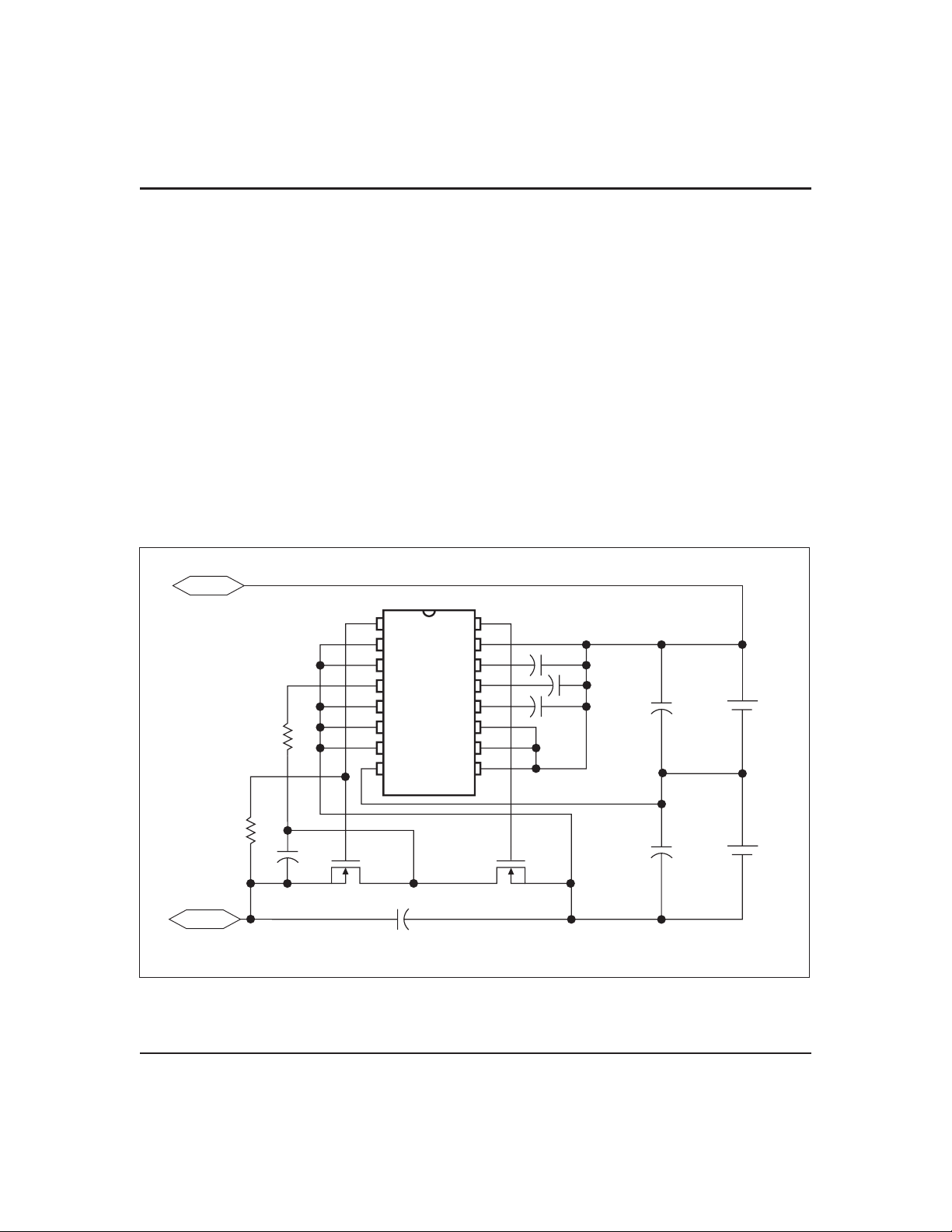
Functional Description
Figure 1 is a block diagram outlining the major components of the bq2058T. Figure 2 shows a low-side control
connection diagram. The following sections detail the
various functional aspects of the bq2058T.
Thresholds
The bq2058T monitors the lithium ion pack for the conditions listed below. Shown with these conditions are
the respective thresholds used to determine if that condition exists:
Overvoltage (VOV)
■
Undervoltage (VUV)
■
Overcurrent (V
■
Charge Enable (VCE)
■
Charge Detect (VCD)
■
POS
OCH,VOCL
R
2
)
2N
2N
2N
1N
DSG
V
UVD
OVD
OCD
V
CSH
BAT
CHG
CTL
V
SS
CSL
BAT
BAT
BAT
BAT
bq2058T
The bq2058T samples a cell every 60ms (typical). Every
sample is a fully differential measurement of each cell.
During this sample period, the bq2058T compares the
measurements with these thresholds to determine if any
of the these conditions exist:V
OV,VUV
,and VCE.
Overcurrent and charge detect are conditions that are
not sampled, but are continuously monitored.
Initialization
On initial power-up, such as connecting the battery pack
for the first time to the bq2058T,the bq2058T enters the
low-power sleep mode, disabling the DSG output. It is
recommended that a top to bottom cell connection
be made at pack assembly for proper initialization. A charging supplymust be applied to the bq2058T
circuit to enable the pack. See Low-Power Sleep Mode
and Charge Detect sections.
CC
CC
1P
C
1
C
2
C
3
C
4
BAT1
NEG
R
1
C
7
Q
1
C
6
Q
2
Figure 2. 2-Cell Connection Diagram, Low-Side Control
4
C
5
FG2058T1.eps
BAT2
July 1997
Page 5

bq2058T
Low-Power Sleep Mode
The bq2058T enters the low-power sleep mode in two
different ways:
1. On initial power-up.
2. After the detection of an undervoltage condi-
UV
.
tion–V
When the bq2058T enters the low-power sleep mode,
DSG is driven low and the device consumes 0.7µA (typical). The bq2058T only comes out of low-power sleep
mode when a valid charge detect condition exists.
Charge Detect
The bq2058T continuously monitors for a charge detect
condition. A valid charge detect condition exists when either of the conditions is true:
CSL < BAT
CSH > BAT
- 70mV (VCD)
2N
+ 70mV (VCD)
1P
A valid charge detect enables the DSG output, allowing
charging of the lithium ion cells. This is accomplished
by applying the charging supply to the pack.
Undervoltage
Undervoltage (or overdischarge) protection is asserted
when any cell voltage drops below the VUVthreshold
and remains below the VUVthreshold for a time
exceeding a user-configurable delay (t
). The DSG
UVD
output is driven low, disabling the discharge of the pack.
The bq2058T then enters the low-power sleep mode.
VUVis defined as follows:
= 2.25V
V
UV
Overvoltage
Overvoltage (or overcharge) protection is asserted when
any cell voltage exceeds the VOVthreshold and remains
above the VOVthreshold for a time exceeding a userconfigurable delay (t
high impedance state, disabling charge into the battery
pack. Since the charge control output is an open drain
output, a pull-down resistor is needed from the CHG pin
to the negative side of the pack. This pulls the gate of
the charge FET low when the CHG pin goes to high impedance. Charging is disabled until a valid charge enable exists. See Charge Enable section.
Important note: If any battery pin floats (BAT
BAT1N,BAT2N), the bq2058T assumes an overvoltage has occurred.
Because of different manufacturers’ specifications for
overvoltage thresholds, the bq2058T can be available
with different V
different voltage thresholds.
July 1997
OV
). The CHG pin goes to the
OVD
1P
options. Table 1 summarizes these
Table 1. Overvoltage Threshold Options
Part # VOVLimit
bq2058T 4.25V
bq2058TR 4.35V
The overvoltage threshold limits are programmed
at Benchmarq. The bq2058T is the standard option that is more readily available for sampling
and prototyping purposes. Please contact Benchmarq for other voltage threshold and tolerance
options.
Charge Enable
A valid charge enable indicates that an overvoltage
(overcharge) condition no longer exists and that the
pack is ready to accept further charge. Once overvoltage
protection is asserted, charging will not be enabled until all cell voltages fall below VCE. The VCEthreshold is
a function of V
and changes with different VOVlim-
OV,
its.
V
CE=VOV
- 150mV
Overcurrent
The bq2058T detects an overcurrent (or short circuit)
condition only in the discharge direction. Overcurrent
protection is asserted when either of the conditions occurs and remain for a time exceeding a userconfigurable delay (t
where:
V
OCL
V
OCH
When either of these conditions occurs, DSG is driven
low, disconnecting the load from the pack. DSG remains
low until both of the voltage conditions are false, indicating removal of the short-circuit condition. The user
can facilitate clearing these conditions by inserting the
battery pack into a charger.
The high-side overcurrent sense can be disabled by con-
,
necting CSH to BAT
greater than BAT1P. If high-side detection is disabled,
low-side detection must be used with CSL.
The FETs in the charge/discharge path controlled by the
CHG and DSG pins affect the overcurrent level. The
on-resistance of these FETs need to be taken into account when determining overcurrent levels.
):
OCD
CSL > BAT
CSH < BAT1P-V
2N+VOCL
OCH
= 160mV (low-side detect)
= 160mV (high-side detect)
. This ensures that CSH is never
1P
5
Page 6
bq2058T
CHG and DSG States
The CHG and DSG output truth table is shown below:
Condition CHG pin DSG pin
Normal operation High High
Overvoltage Z High
Undervoltage High Low
Overcurrent High Low
Floating battery input Z Indeterminate
CTL = high Z Low
The polarities of CHG and DSGare mask programmable
at Benchmarq. Push-pull vs. open-drain configuration is
also mask-configurable at Benchmarq. Please contact
Benchmarq for availability of these variations.
PackDisable Input–CTL
The CTL pin is used to electrically disconnect the battery from the pack terminals through an externally supplied signal. When CTL is taken high, CHG goes to the
high impedance state and DSG is driven low. Any load
on the pack terminals will be interpreted as an overcurrent condition by the bq2058T with the overcurrent delay timer held in reset. When the CTL pin is driven low,
the overcurrent delay timer is allowed to start. If the
programmed delay (t
recovery circuit, if implemented, will be unable to correct the overcurrent situation prior to the delay timeout. It is recommended that a delay time of greater than
10ms (C
≥ 0.01µF) be used if the CTL pin function
OCD
is to be utilized.
) is too short, the overcurrent
OCD
Important note: If CTL floats, it is internally
pulled high making both DSG and CHG inactive,
thus disabling the pack. If CTL is not used, it
should be tied to V
SS
.
The polarity of CTL is mask-programmable at Benchmarq. Please contact Benchmarq for other polarity options.
Protection DelayTimers
The delay time between the detection of an overcurrent,
overvoltage, or undervoltage condition and the deactivation of the CHG and/or DSG outputs is user-configurable
by the selection of capacitorvalues between VCCand OCD,
OVD,and UVD pins (respectively. SeeTable2 below.
The fault condition must persist through the entire delay period, or the bq2058T may not deactivate either
FET control output.
Figure 3 shows a step-by-step event cycle for the
bq2058T.
Table 2.Protection Delay Timers
Protection
Feature
Overcurrent t
Overvoltage t
Undervoltage t
Delay
Period
OCD
OVD
UVD
Capacitor from
VCCto:
OCD
OVD
UVD
Capacitor Time
0.010µF
0.100µF
0.100µF
Notes: 1. The delay time versus capacitance can be approximated bythe following equations:.
For t
For t
:t
OCD
OVD,tUVD
(s)
:t
(s)
≈ 1.2 ∗ C
≈ 9.5 ∗ C
, where 0.001µF ≤ C≤ 0.1µF
(µf)
, where 0.01µF ≤ C≤ 1µF
(µf)
2. Overvoltage andundervoltage conditions are sampled by thebq2058T. The delay in Table 2 is in
addition to the time required for the bq2058T todetect the violation, which may vary from 0 to
120 ms depending on where in the sampling periodthe violation occurs. Overcurrent is continuously
monitored and is subject to a delay of approximately 1.5ms.
Typical
12ms
950ms ±40%
950ms ±40%
6
Tolerance
±40%
July 1997
Page 7

Cell Voltage
0
1 2 3 4 65 7 8 9 10 11 12
V
OV
V
CE
bq2058T
V
UV
CSL
BAT2N + 160mV (V
BAT2N - 70mV (VCD)
DSG
t
OCD
t
UVD
CHG
t
OVD
CTL
TD2058T1.eps
Figure 3. Protector Event Diagram
Event Definition:
0: The bq2058T is inthe low-power sleep mode because oneor more of the cell voltagesare below V
1: A charger is appliedto the pack, causing the difference between CSL and BAT
than 70mV. This awakens the bq2058T,and the discharge pin DSG goes high.
2: One or more cellscharge to a voltage equal to V
, initiating the overvoltagedelay timer.
OV
3: The overvoltage delay timeexpires, causing CHGto go to high impedance (pulledlow externally).
4: All cell voltages fallbelow V
, causing CHG togo high.
CE
5: Stop charging, apply a load.
6: An overcurrent condition isdetected, initiating the overcurrent delay timer.
7: The overcurrent delay timeexpires, causing DSGto go low.
8: The overcurrent condition isno longer present. DSG is driven high.
9: Pin CTL is drivenhigh; both DSG and CHG go inactive.
10: PinCTL is driven low; both DSG and CHG go activeresuming their normal function.
11: Oneor more cells fall below V
12: Oncethe overdischarge delay timer expires, if any of the cells is below V
, initiating the overdischargedelay timer.
UV
UV
DSG low and enters the low-power sleep mode.
to become greater
2N
, the bq2058T drives
UV
OCL
.
)
July 15, 1997
7
Page 8

bq2058T
Absolute Maximum Ratings
Symbol Parameter Value Unit Conditions
V
CC
T
OPR
T
STG
T
SOLDER
I
IN
Supply voltage 18 V Relative to V
Operating temperature -30 to +70 °C
Storage temperature -55 to +125 °C
Soldering temperature 260 °C For 10 seconds
Maximum input current
±100 µA
All pins except VCC,V
SS
SS
Notes: 1 Permanent device damage may occur if Absolute Maximum Ratings are exceeded. Functional
operation should be limited to the Recommended DC OperatingConditions detailed in this data sheet.
Exposure to conditions beyond the operational limits for extendedperiods of time may affect device
reliability.
2. Internal protectiondiodes are in place on everypin relative to V
Any pin
(except CHG)
V
CC
CHG pin
V
SS
FG2058tx .eps
V
CC
and VSS. See picture below.
CC
July 1997
8
Page 9

bq2058T
DC Electrical Characteristics (T
A=TOPR)
Symbol Parameter Minimum Typical Maximum Unit Conditions/Notes
V
OH
V
OL
V
OP
V
IL
V
IH
I
CCA
I
CCS
R
CELL
DC Thresholds (T
Output high voltage VCC- 0.5 - - V
Output low voltage - - VSS+ 0.5 V
IOH=10µA, CHG, DSG
IOL=10µA, CHG, DSG
Operating voltage 0 - 9.0 V VCCrelative to V
Input low voltage - - VSS+ 0.5 V Pin CTL
Input high voltage VSS+ 2.0 - - V Pin CTL
Active current - 12 25
Sleep current - 0.7 1.5
Input impedance - 10 -
µA
µA
MΩ
Pins BAT
BAT1N, and BAT
2N,
A=TOPR)
SS
Symbol Parameter Value Unit Tolerance Conditons
V
Overvoltage threshold
OV
4.25 V
±55mV
See note 1
Table 1 Customer option
V
V
V
V
V
t
OVD
t
UVD
t
OCD
Charge enable threshold VOV- 150mV V
CE
Undervoltage threshold 2.25 V
UV
Overcurrent detect
OCH
high-side
Overcurrent detect
OCL
low-side
Charge detect threshold 70 mV -60mV, +80mV
CD
Overvoltage delay
threshold
Undervoltage delay
threshold
Overcurrent delay threshold
160 mV
160 mV
950 ms
950 ms
12 ms
±55mV
±100mV
±35mV
±35mV
±40%
±40%
±40%
C
= 0.100µF
OVD
TA=30°C
See note 2
C
= 0.100µF
UVD
TA=30°C
See note 2
C
= 0.01µF
OCD
T
=30°C
A
1P
Notes: 1. Standard device. Contact Benchmarq for different thresholds and tolerance options
2. Does not includecell sampling delay, which may add up to 120ms of additional delay until the
condition is detected.
July 1997
9
Page 10

bq2058T
Typical Characteristics
– Overvoltage – V
V
OV
4.280
4.270
4.260
4.250
4.240
4.230
4.220
4.210
bq2058T 4.25V OVERVOLTAGE THRESHOLD
FREE-AIR TEMPERATURE
Measurement accuracy ± 2mV
-20 -10 0 10 20 30 40 50 60 70
-30
TA – Free-Air Temperature –
VS
˚
C
Figure 4
10
July 1997
Page 11

Data Sheet Revision History
Change No. Page No. Description Nature of Change
1 5 CHG pin output state CHG pin state at overvoltage and floating battery
1 9 Overcurrent limits
1 9 Charge detect threshold Was:70mV +10mV, +80mV
2 4 Overvoltage options, Table 1 Added bq2058TR
2 4 Figure 2 Corrected schematic
2 6, 9 Delay thresholds
2 7 DSG and CHG timing diagram Inverted lines for proper logic levels
2 7 Timing Diagram
2 8 Maximum input current Added I
29V
tolerance
OV
2 9 Overcurrent limits
29V
OP
input was low, is nowZ
Was:V
Is: V
= 100mV ±25mV
OCL
= 150mV ±25mV
OCL
Is: 70mV -60mV,+80mV
Was:t
Is: t
= 10ms ±30%
OCD
t
= 800ms ±30%
OVD
t
UVD
= 12ms ±40%
OCD
t
= 950ms ±40%
OVD
t
= 950ms ±40%
UVD
= 800ms ±30%
Was:CSH timing
Is: CSL timing
IN
Was:±50mV
Is: ±55mV
Was:V
Is: V
= 160mV +25mV
OCH
V
= 150mV +25mV
OCL
= 160mV +35mV
OCH
V
= 160mV +35mV
OCL
Was:0V min,18V max
Is: 4V min, 9V max
bq2058T
Note: Change1=June19,1997 changes from April 22, 1997.
Change2=July1997 changes from June 19, 1997
July 1997
11
Page 12

bq2058T
SN: 16-Pin SN(0.150" SOIC
e
H
C
L
D
E
A
A1
B
.004
)
16-Pin SN(0.150" SOIC
Inches Millimeters
Dimension
A 0.060 0.070 1.52 1.78
A1 0.004 0.010 0.10 0.25
B 0.013 0.020 0.33 0.51
C 0.007 0.010 0.18 0.25
D 0.385 0.400 9.78 10.16
E 0.150 0.160 3.81 4.06
e 0.045 0.055 1.14 1.40
H 0.225 0.245 5.72 6.22
L 0.015 0.035 0.38 0.89
Min. Max. Min. Max.
)
12
July 1997
Page 13

Ordering Information
bq2058T XXXX
Device:
bq2058T
Standard Device:
Blank = Standard device
XXXX = Customer code assigned by Benchmarq
PackageOption:
SN = 16-pin narrow SOIC
Overvoltage Threshold
Blank = 4.25V (Standard device)
Contact factory for availability of other thresholds
bq2058T Lithium Ion Pack Supervisor
July 1997
Package Devices
T
A
-30°Cto
+70°C
Note: bq2058TSN isStandard Device
Contact factory for availability of other thresholds and tolerances.
VOVThreshold 16-pin Narrow SOIC (SN)
4.25V bq2058TSN
4.35V bq2058TRSN
13
Page 14

Notes
14
July 1997
Page 15

Notes
July 1997
15
Page 16

bq2058T
BENCHMARQ Microelectronics,Inc.
17919 Waterview Parkway
Dallas, Texas 75252
Fax: (972) 437-9198
Tel: (972) 437-9195
E-mail: benchmarq @ benchmarq.com
World Wide Web: http://www.benchmarq.com
Copyright © 1997,BENCHMARQ Microelectronics,Inc. Allrights reserved.
No part of this data sheet may be reproduced in any form or means,without express permission from Benchmarq.
Benchmarq reserves the right to make changes in its products without notice.
Benchmarq assumes no responsibility for use of any products or circuitry described within. No license for use of in-
tellectual property (patents,copyrights,or other rights)owned by Benchmarq or other parties is granted or implied.
Benchmarq does not authorize the use of its components in life-support systems where failure or malfunction may
cause injury to the user. If Benchmarq components are used in life-support systems, the user assumes all responsibilities and indemnifies Benchmarq from all liability or damages.
Benchmarq is a registered trademark of BENCHMARQ Microelectronics, Inc. Printed in U.S.A.
July 1997
16
Page 17

PACKAGE OPTION ADDENDUM
www.ti.com
30-Mar-2005
PACKAGING INFORMATION
Orderable Device Status
(1)
Package
Type
Package
Drawing
Pins Package
Qty
Eco Plan
BQ2058TRSN-C2 OBSOLETE SOIC D 16 TBD Call TI Call TI
BQ2058TSN-C2 OBSOLETE SOIC D 16 TBD Call TI Call TI
(1)
The marketing status values are defined as follows:
ACTIVE: Product device recommended for new designs.
LIFEBUY: TI has announced that the device will bediscontinued, and a lifetime-buy period isin effect.
NRND: Not recommended for new designs. Device is in production to support existing customers, but TI does not recommend using this part in
a new design.
PREVIEW: Device has been announced but is not inproduction. Samples may or may notbe available.
OBSOLETE: TI has discontinued the production of the device.
(2)
Eco Plan - The planned eco-friendly classification: Pb-Free (RoHS) or Green (RoHS & no Sb/Br) - please check
http://www.ti.com/productcontent for the latest availability information and additional productcontent details.
TBD: The Pb-Free/Green conversion plan has not been defined.
Pb-Free (RoHS): TI's terms "Lead-Free" or "Pb-Free" mean semiconductor products that are compatible with the current RoHS requirements
for all 6 substances, including the requirement that lead not exceed 0.1% by weight in homogeneous materials. Where designed to be soldered
at high temperatures, TI Pb-Free products are suitable foruse in specified lead-free processes.
Green (RoHS & no Sb/Br): TI defines "Green" to mean Pb-Free (RoHS compatible), and free of Bromine (Br) and Antimony (Sb) based flame
retardants (Br or Sb do not exceed 0.1% byweight in homogeneous material)
(3)
MSL, Peak Temp. -- The Moisture Sensitivity Level rating according to the JEDEC industry standard classifications, and peak solder
temperature.
(2)
Lead/Ball Finish MSL Peak Temp
(3)
Important Information and Disclaimer:The information provided on this page represents TI's knowledge and belief as of the date that it is
provided. TI bases its knowledge and belief on information provided by third parties, and makes no representation or warranty as to the
accuracy of such information. Efforts are underway to better integrate information from third parties. TI has taken and continues to take
reasonable steps to provide representative and accurate information but may not have conducted destructive testing or chemical analysis on
incoming materials and chemicals. TI and TI suppliers consider certain information to be proprietary, and thus CAS numbers and other limited
information may not be available for release.
In no event shall TI's liability arising out of such information exceed the total purchase price of the TI part(s) at issue in this document sold by TI
to Customer on an annual basis.
Addendum-Page 1
Page 18

IMPORTANT NOTICE
Texas Instruments Incorporated and its subsidiaries (TI) reserve the right to make corrections, modifications,
enhancements, improvements, and other changes to its products and services at any time and to discontinue
any product or service without notice. Customers should obtain the latest relevant information before placing
orders and should verify that such information is current and complete. All products are sold subject to TI’s terms
and conditions of sale supplied at the time of order acknowledgment.
TI warrants performance of its hardware products to the specifications applicable at the time of sale in
accordance with TI’s standard warranty. Testing and other quality control techniques are used to the extent TI
deems necessary to support this warranty . Except where mandated by government requirements, testing of all
parameters of each product is not necessarily performed.
TI assumes no liability for applications assistance or customer product design. Customers are responsible for
their products and applications using TI components. To minimize the risks associated with customer products
and applications, customers should provide adequate design and operating safeguards.
TI does not warrant or represent that any license, either express or implied, is granted under any TI patent right,
copyright, mask work right, or other TI intellectual property right relating to any combination, machine, or process
in which TI products or services are used. Information published by TI regarding third-party products or services
does not constitute a license from TI to use such products or services or a warranty or endorsement thereof.
Use of such information may require a license from a third party under the patents or other intellectual property
of the third party, or a license from TI under the patents or other intellectual property of TI.
Reproduction of information in TI data books or data sheets is permissible only if reproduction is without
alteration and is accompanied by all associated warranties, conditions, limitations, and notices. Reproduction
of this information with alteration is an unfair and deceptive business practice. TI is not responsible or liable for
such altered documentation.
Resale of TI products or services with statements different from or beyond the parameters stated by TI for that
product or service voids all express and any implied warranties for the associated TI product or service and
is an unfair and deceptive business practice. TI is not responsible or liable for any such statements.
Following are URLs where you can obtain information on other Texas Instruments products and application
solutions:
Products Applications
Amplifiers amplifier.ti.com Audio www.ti.com/audio
Data Converters dataconverter.ti.com Automotive www.ti.com/automotive
DSP dsp.ti.com Broadband www.ti.com/broadband
Interface interface.ti.com Digital Control www.ti.com/digitalcontrol
Logic logic.ti.com Military www.ti.com/military
Power Mgmt power.ti.com Optical Networking www.ti.com/opticalnetwork
Microcontrollers microcontroller.ti.com Security www.ti.com/security
Telephony www.ti.com/telephony
Video & Imaging www.ti.com/video
Wireless www.ti.com/wireless
Mailing Address: Texas Instruments
Post Office Box 655303 Dallas, Texas 75265
Copyright 2005, Texas Instruments Incorporated
Page 19

Copyright © Each Manufacturing Company.
All Datasheets cannot be modified without permission.
This datasheet has been download from :
www.AllDataSheet.com
100% Free DataSheet Search Site.
Free Download.
No Register.
Fast Search System.
www.AllDataSheet.com
 Loading...