

Page 1
查询bq2057/C/W/T供应商
bq2057/C/W/T
Advanced Li-Ion Linear Charge
Management IC
Features
Ideal forsingle- and dual-cell Li-Ion
packs with coke or graphite anodes
0.3V dropout voltage
AutoComp™ dynamic compensa
tion ofbattery pack’s internal im
pedance
Optional temperature-monitoring
before and during charge
Integrated voltage and current
regulation with programmable
charge-current and high- or
low-side current sensing
Integrated cell conditioning for
reviving deeply discharged cells
and minimizing heat dissipation
during initial stage ofcharge
Better than
tion accuracy
Charge status output for LED or
host processor i nterface
Automatic battery-recharge feature
Charge termination by minimum
current
Low-power sleep mode
Packaging: 8-pin SOIC, 8-pin
TSSOP
±
1% voltage regula-
General Description
The BENCHMARQ bq2057 series
advanced Li-Ion linear chargemanagement ICs are designed for
cost-sensitive and compact portable
electronics. They combine high-
accuracy current and voltage
regulation, battery conditioning,
temperature monitoring, charge
termination, charge-status indication, and AutoComp charge-rate
compensation in a single 8-pin IC.
The bq2057 continuously measures
battery temperature using an external thermistor. For safety reasons,
the bq2057 inhibits charge until the
battery temperature is within
user-defined thresholds. The bq2057
then charges th e battery in three
phases: conditioning, constant current, and constant voltage. If the battery voltage is below the low-voltage
threshold V
trickle-charges to condition the battery. The conditioning charge rate is
set at approximately 10% of the regulation current. The conditioning
current also minimizes heat dissipation in t he external pass-element
during the initial stage ofcharge.
After conditioning, the bq2057 ap
plies a constant current to the bat
tery. An external sense-resistor sets
the magnitude of the current. The
sense-resistor can be on either the
, th e bq2057
MIN
low or t h e high side of th e battery
without additional components. The
constant-current phase continues
until the battery reaches th e
charge-regulation voltage.
The bq2057 then begins the con
stant-voltage phase. The accuracy of
the voltage regulation is better than
±
1% over the operating-temperature
and supply-voltage ranges. For sin
gle and dual cells with either coke or
graphite anodes, the bq2057 is of
fered in four fixed-voltage versions:
4.1V, 4.2V, 8.2V, and 8.4V. Charge
stops when the current tapers to the
charge termination threshold,
V
. The bq2057 automatically re-
TERM
starts the charge if the battery voltage falls belowthe V
The designer also may use the
AutoComp feature to reduce charging time. This proprietary technique
allows safe and dynamic compensation for t h e internal impedance of
the battery pack during charge.
Available Options
Part Number
-
-
bq2057 4.1V
bq2057C 4.2V
bq2057T 8.2V
bq2057W 8.4V
threshold.
RCH
Charge
Regulation
Voltage
-
-
-
Pin Connections
SLUS025B–JANUARY2000–REVISED JUNE 2000
Pin Names
SNS Current-sense input
BAT Battery-voltage input
V
TS Temperature sense
CC
Supply voltage
input
1
STAT Charge status output
V
CC Charge control output
COMP Charge-rate
Ground input
SS
compensation input
Page 2
bq2057
Pin Descriptions
SNS Current-sense input
Battery current is sensed via the voltage de
veloped on this pin by an external sense re
sistor.
BAT Battery voltage input
Voltage sense-input tied directly to the posi
tive side ofthe battery.
V
CC
TS Temperaturesenseinput
VCCsupplyinput
Input for an external battery-temperature
monitoring circuit. Connecting this input to
Vcc/2 disables th i s feature.
BAT
STAT Charge status output
Tri-state indication of charge-in-progress,
charge-complete, andtemperature fault.
-
V
SS
-
Ground input
CC Charge-control output
Source-follower output that drives a n exter
-
nal pass-transistor for current and voltage
regulation.
-
COMP Charge-rate compensation input
Sets the charge-rate compensation level. The
voltage-regulation output may be pro
grammed to vary as a function ofthe charge
current delivered to the battery.
V
SS
V
CC
POWER
ON
RESET
CC
COMP
SNS
TS
K
COMP
V
REG
CONTROL
V
SNS
V
, V
TS1
TS2
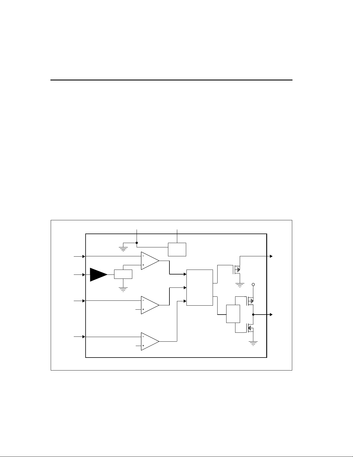
Figure 1. Functional Block Diagram
2
BLOCK
LED
STAT
VCC
STAT
2057FBD.eps
Page 3
bq2057
Sleep Mode
LED = Hi-Z
V
≤ V
BAT
MIN
NO
Current
Regulation
Phase
LED = High
Voltage
Regulation
Phase
LED = HIGH
NO
YES
YES
NO
VCC > V
BAT
YES
Temperature
Check
TS > V
TS1
TS < V
TS2
Conditioning
Phase
LED = High
I
REG
I
≤ V
BAT
10
YES
NO
Temperature
Fault
LED = Hi-Z
Charge
Complete
LED = LOW
YES
≤ V
BAT
RCH
2057OFC.eps
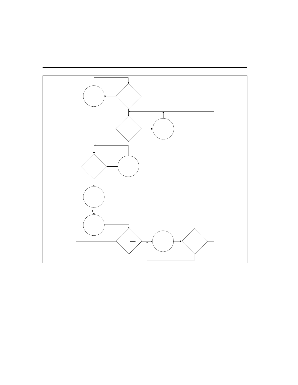
Figure 2. Operational Flow Chart
Functional Description
Figure 1 is a functional block diagram, Figure 2 a n oper
ational flow chart, an d Figure 3 a typical charger sche
matic forthe bq2057.
Charge Qualification and Conditioning
When power is applied, the bq2057 starts a charge-cycle
if a battery is already present or when a battery is in
NO
serted. Charge qualification is based on battery temper
ature and voltage. The bq2057 suspends charge if the
battery temperature is outside the V
and suspends charge until the battery temperature is
within th e allowed range. The bq2057 also checks the
TS1
to V
battery voltage. If the battery voltage is below the
low-voltage threshold V
trickle-charge to condition the battery. The conditioning
charge rate I
-
regulation current. The conditioning current also mini
is set at approximately 10% of the
COND
, th e bq2057 uses
MIN
3
TS2
-
range
-
Page 4
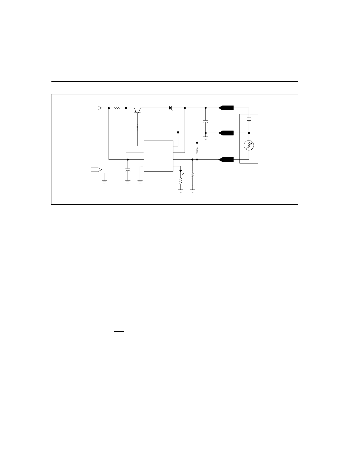
bq2057
R
DC+
DC-
SNS
0.2Ω
0.1µF
Q1
FZT788B
R1
1kΩ
78
CC
1
SNS
3
V
CC
6
V
C2
SS
bq2057
COMP
BAT
STAT
D2
V
CC
V
CC
2
4
TS
5
D1
R2
2kΩ
R
T1
R
T2
C1
0.1µF
PACK+
PACK-
TEMP
Figure 3. Low-Dropout Single- or Dual-Cell Li-Ion Charger
Battery
2057ldc.eps
NTC
Pack
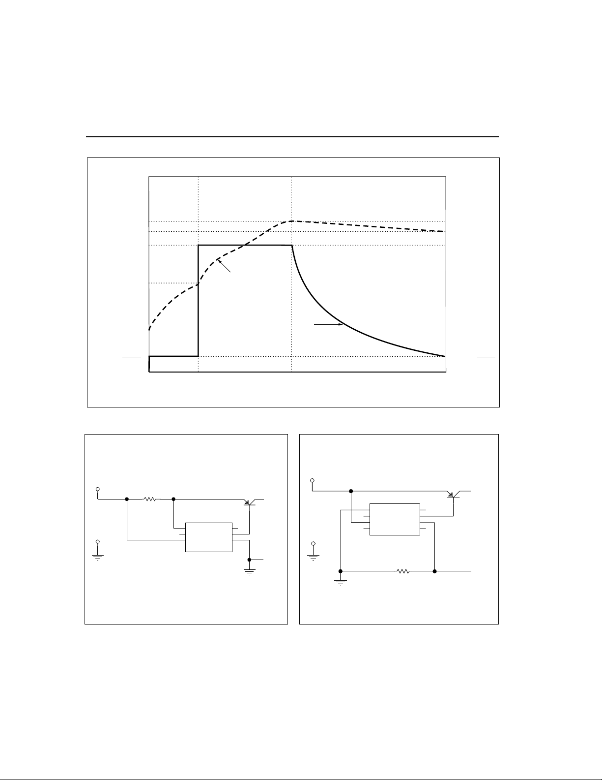
mizes heat dissipation in the external pass-element during t he initial stage ofcharge. See Figure 4 for a typical
charge-algorithm.
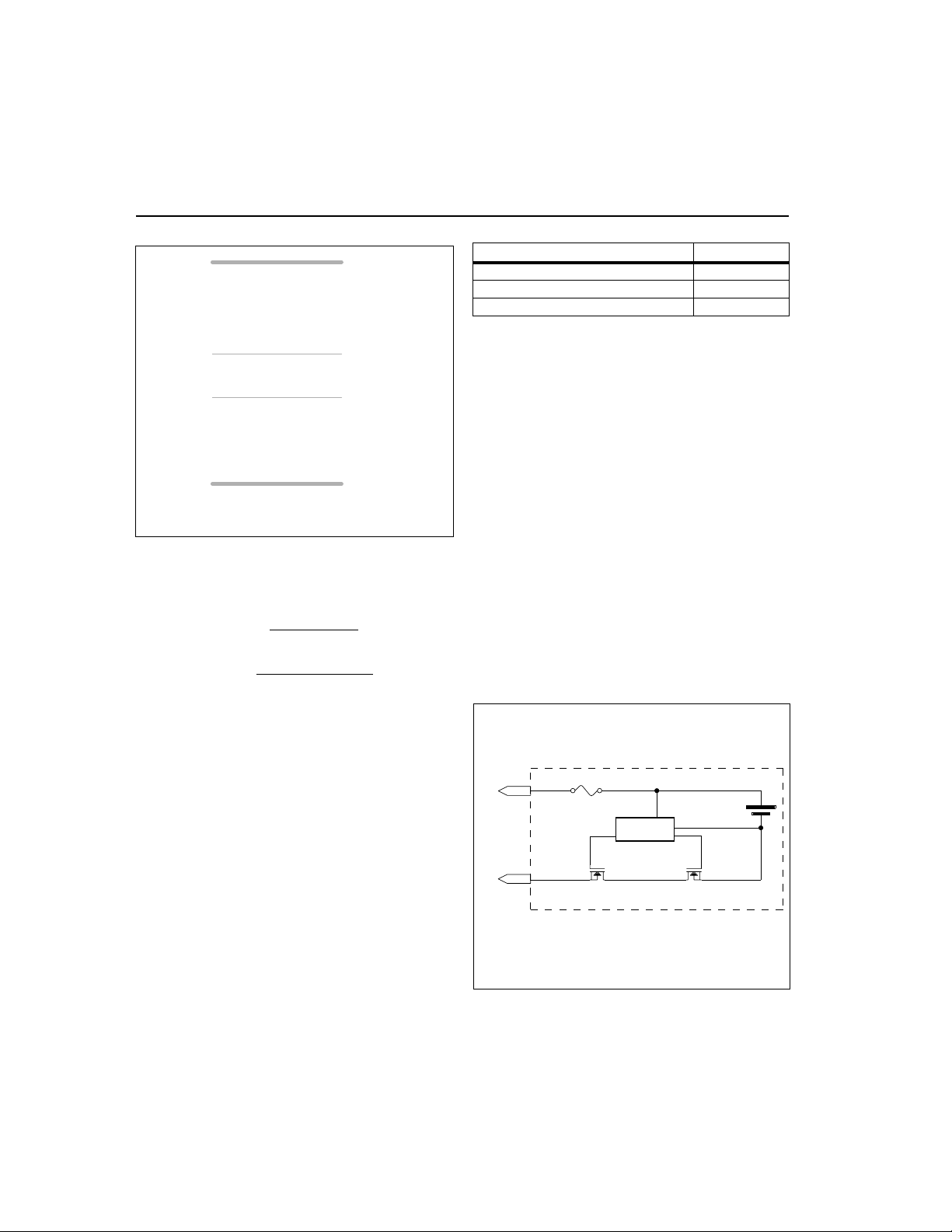
Current Regulation
The bq2057 regulates current while the battery-pack
voltage i s less than the regulation voltage, V
bq2057 monitors charge current a t the SNSinput by the
voltage drop across a sense-resistor, R
the battery pack. I n high-side current sensing configura
tion (Figure 5), R
pins, and in low-side sensing (Figure 6) the R
is placed between the Vcc and SNS
SNS
, in series with
SNS
placed between Vss (battery negative) and SNS (charger
ground) pins.
Charge-current feedback, applied through pin SNS,
maintains regulation around a threshold ofV
lowing formula calculates the value ofthe sense resistor:
V
SNS
SNS
=
REG
I
where I
R
is the desired charging current.
REG
SNS
. The
REG
SNS
. The fol
Voltage Monitoring and Regulation
Voltage regulation feedback is through pin BAT. This in
put is tied directly to the positive side of the battery
pack. The bq2057 monitors t he battery-pack voltage be
tween the BAT and V
four fixed-voltage versions for single- and dual-cells with
pins. The bq2057 is offered in
SS
either coke or graphite anodes: 4.1V, 4.2V, 8.2V, and
8.4V.
Other regulation voltages can be achieved by adding a
voltage divider between the positive and negative terminals of th e battery pack. The voltage divider presents a
scaled battery pack voltage to BAT input. (See Figures 7
and 8.) The resistor values R
divider ar e calculated bythe following equation:
R
B1
-
is
=∗
B2
R
and RB2for the voltage
B1
V
CELL
N
−
1
REG
V
where
N=Number ofcellsin series
-
V
= Desired regulation voltage pe r cell
CELL
Charge Terminationand Re-Charge
The bq2057 monitors the charging current during the
voltage-regulation phase. The bq2057 declares a “batterycomplete” condition a nd terminates charge when the
current tapers off to the charge termination threshold,
V
. A new charge cycle begins when the battery volt
TERM
age falls below the
-
-
VRCH
threshold.
-
4
Page 5
bq2057
I
COND
Low-Current
Conditioning
Phase
V
PACK
V
REG
I
REG
V
MIN
I
REG
=
10
Current
Regulation
Phase
V
BAT
(Shown with the optional AutoComp feature)
Voltage Regulation Phase
I
BAT
GR2057b.eps
I
FULL
I
REG
=
10
Figure 4. Typical Charge Algorithm
DC+
R
SNS
DC-
2057HSCS.eps
bq2057
1
SNS
2
BAT
3
V
CC
4
TS
COMP
CC
V
STAT
8
7
6
SS
5
Figure 5. High-Side Current Sensing
BAT+
BAT-
DC+
bq2057
DC-
1
2
3
4
SNS
BAT
V
CC
TS
COMP
CC
V
STAT
R
SNS
SS
Figure 6. Low-Side Current Sensing
5
BAT+
8
7
6
5
BAT-
2057LSCS1.eps
Page 6

bq2057
DC+
R
SNS
DC-
DC+
BAT+
BAT+
R
B1
bq2057
1
2
3
4
SNS
BAT
V
CC
TS
COMP
CC
V
STAT
SS
R
8
7
6
5
B2
BAT-
2057OVDHSC.eps
DC-
bq2057
1
SNS
2
BAT
3
V
CC
4
TS
COMP
CC
V
STAT
8
7
6
SS
5
R
B1
R
B2
R
SNS
2057OVDLSC.eps
BAT-
Figure 7. Optional Voltage Divider for
Non-Standard Regulation Voltage,
(High-Side Current Sensing)
Temperature Monitoring
The bq2057 continuously monitors temperature by measuring the voltage between the TS and V
tive- or a positive-temperature coefficient thermistor
(NTC, PTC) and an external voltage-divider typically develop this voltage. (See Figure 9.) The bq2057 compares
this voltage against its internal V
to determine if charging is allowed. (See Figure 10.) The
TS1
temperature sensing circuit is immune to any fluctuation
in the V
the internal thresholds (V
V
CC
, since both the external voltage divider and
CC
.
DC+ DC+
RT1
DC-
RT2
and V
TS1
R
SNS
bq2057
1
SNS
2
BAT
3
V
CC
4
TS
pins. A nega-
SS
and V
TS2
thresholds
TS2
) are referenced to
8
COMP
7
CC
6
V
SS
5
STAT
BAT+
BAT-
Thermistor
Figure 8. Optional Voltage Divider for
Non-Standard Regulation Voltage,
(Low-Side Current Sensing)
The resistor values ofR
following equations:
ForNTCthermistors
R=
T1
R=
T2
1
SNS
2
BAT
3
V
CC
4
TS
DC-
and RT2are calculated by th e
T1
()
∗∗
TH TC
5R R
()()
∗
TC TH
3R-R
()
∗∗
TH TC
5R R
()()()
∗−∗
TC TH
2R 7R
BAT+
bq2057
COMP
V
STAT
8
7
CC
6
SS
5
R
T1
Thermistor
R
T2
BAT-
R
SNS
2057TSC.eps
High-Side Current Sensing Low-Side Current Sensing
Figure 9. Temperature Sensing Circuits
6
Page 7
bq2057
V
CC
Temp Fault
V
TS2
Normal Temp Range
V
TS1
Temp Fault
V
SS
2057TSIT.eps
Figure 10. bq2057 TS Input Thresholds
ForPTC thermistors
5R R
TH TC
∗∗
R=
T1
R=
T2
()()
TH T C
3R-R
∗
()
∗∗
TH TC
5R R
()()()
∗−∗
TH TC
2R 7R
Condition STAT Pin
Battery conditioning and charging High
Charge complete Low
Temperature fault or sleep mode High-Z
Automatic Charge-Rate
Compensation
To reduce charging time, the bq2057 uses the propri
etary AutoComp technique to compensate safely for in
ternal impedance ofthe battery pack.
Figure 11 outlines th e major components of a single-cell
Li-Ion battery pack. The Li-Ion battery pack consists of
a cell, protection circuit, fuse, connector, current
sense-resistors, and some wiring. Each of these compo
nents contains some resistance. Total impedance of the
battery pack is the su m of th e minimum resistances of
all battery-pack components. Using the minimum resistance values reduces the odds for overcompensating.
Overcompensating may activate the safety circuit of the
battery pack.
Compensation is through input pin COMP (Figure 12).
A portion of the current-sense voltage, presented
through this pin, is scaled by a factor of K
summed with t h e regulation threshold, V
cess increases t h e output voltage to compensate for the
REG
battery pack’s internal impedance and for undesired
voltage drops i n thecircuit.
and
COMP
. This pro-
-
-
-
where RTCis the cold-temperature resistance and RTHis
the hot-temperature resistance of the thermistor, as
specified by the thermistor manufacturer.
R
or RT2can be omitted if only one temperature set
T1
ting (Hot or Cold) isrequired.
Applying a voltage between the V
oldstopin TS disables t hetemperature-sensing feature.
TS1
and V
TS2
thresh
Low-Power Mode
The bq2057 enters the sleep mode if the VCCfalls below
the voltage at the BAT input. This feature prevents
draining the battery pack during the absence ofV
.
CC
Charge Status Display
The bq2057 reports t he status of the charger on the
tri-state STAT pin. The three states include “charge in
progress, charge complete, andtemperature fault.
-
Wire
R2
FUSE
Discharge
Protection
Controller
Wire
Cell
WireWire
Charge
2057SCLIP.eps
Terminal
-
BAT+
Terminal
BAT-
Figure 11. Typical Components of a
Single-Cell Li-Ion Pack
7
Page 8
bq2057
DC+
DC-
R
COMP2
R
SNS
High-Side Current Sensing
R
1
2
3
4
COMP1
SNS
BAT
V
TS
bq2057
CC
COMP
CC
V
STAT
8
7
6
SS
5
BAT+
Figure 12. AutoComp Circuits
AutoComp setup requires the following information:
Total impedance ofbattery pack (Z
Maximum charging current (I
The voltage drop V
the battery pack can then becalculated by
across the internal impedance of
Z
V
Z=ZPACK
REG
∗
I
The required compensation is then calculated using the
following equations:
V=
COMP
V
COMP
K
REG
Z
)
PACK
)
DC+
COMP2
PACK
BAT+
BAT-
2057AC.eps
is the
bq2057
1
SNS
2
BAT
3
V
CC
4
DC-
where V
is referenced to Vcc i n high-side current-sensing config-
COMP
TS
R
R
SNS
Low-Side Current Sensing
is the voltage on COMP pin. This voltage
COMP1
COMP
CC
V
STAT
8
7
6
SS
5
R
uration and to Vss for low-side sensing. V
voltage across the battery pack.
The values ofR
ing the following equation:
COMP1
V
COMP
SNS
V
and R
COMP2
R
=
COMP2
COMP1 COMP2
R+R
can be calculated us-
V
PACK=VREG
+(K
COMP
∗
V
)
COMP
8
Page 9

Absolute Maximum Ratings
Symbol Parameter Min. Max. Units Notes
V
CC
V
T
T
OPR
T
STG
P
D
VCCrelative to V
VCCrelative to V
SS
SS
Operating ambient temperature -20 70
Storage temperature -40 125
-0.3 +18 V
V
-0.3
+ 0.3
CC
V
°
°
Power dissipation 300 mW
DCvoltage applied on a ny pin (ex
cluding V
CC
C
C
bq2057
-
)
DC Thresholds (T
A=TOPR
and VCC= 4.5–15V unless otherwise specified)
Symbol Parameter Rating Tolerance Unit Notes
4.10
V
REG
Voltage regulation reference
4.20
8.20
8.40
±
1%
±
1%
±
1%
±
1%
105 ±10% mV
110
V
SNS
Curren t regulation reference
±
10%
125 ±10% mV
130 ±10% mV
V For bq2057 only; seeNotes 1, 2, 3
V For bq2057C only; see Notes 1, 2, 3
V For bq2057T only; see Notes 1, 2, 3
V For bq2057W only; see Notes 1, 2, 3
For bq2057 and bq2057C only; see
Note 2
For bq2057 and bq2057C only; see
mV
Note 4
For bq2057T and bq2057W only; see
Note 2
For bq2057T and bq2057W only, see
Note 4
3.0 ±2% V For bq2057 only
V
MIN
Conditioning voltage
reference
3.1 ±2% V For bq2057C only
6.1 ±2% V For bq2057T only
6.3 ±2% V For bq2057W only
K
COMP
V
TS1
V
TS2
V
RCH
V
RCH
V
TERM
Notes:
AutoComp gain 2.2
Lower temperature threshold
Upper temperature threshold
Recharge threshold
Recharge threshold
V
V
0.3
0.6
∗
∗
REG
REG
VCC±
VCC±
- 0.1
- 0.2
±
15%
3% of V
3% of V
±2% V
±2% V
V/V See Notes 1, 5
Voltage at pin TS, relative to V
V
CC
Voltage at pin TS, relative to V
V
CC
Voltage on BAT pin, bq2057 and
bq2057C only
Voltage on BAT pin, bq2057T and
bq2057W only
Charge termination reference -14 ±10mV mV See Note 6
1. VCC=V
2. Fo r high-side current-sensing configuration
+ 0.3V to 15V
BAT
3. For low-side current sensing configuration, t he tolerance is ±1%forT
4. For low-side current-sensing configuration
=25°and ±1.2% for TA=T
A
5. 2.4 and ±15% for bq2057T and bq2057W in low-side current sensing configuration
6. Voltage at pin SNS, relative to V
forhigh-side sensing, and to VSSfor low-side sensing, 0°C≤TA≤50°
CC
SS
SS
.
OPR
C
9
Page 10

bq2057
DC Electrical Characteristics (T
A=TOPR
, and VCC= 4.5 - 15V unless otherwise specified))
Symbol Parameter Min Typical Max Units Notes
V
I
CC
I
CCS
V
V
I
IH
I
SNK
V
Note:
CC
OL
OH
OLCC
Supply voltage 4.5 - 15 V
Operating current - 2 4 mA Excluding external loads
Sleep current
-36
--10
For bq2057 and bq2057C, see note
µ
A
For bq2057T and bq2057W, see note
µ
A
Output-low voltage - 0.4 0.6 V IOL= 10mA; ST AT pin
Output-high voltage VCC- 0.5 - - V IOH= 5mA; STA Tpin
BAT input, V
µ
A
SNS, COMP, and TS inputs,
µ
A
V
SNS=VCOMP=VTS
BAT=VREG
Input leakage current
--1
--5
Sink current 5 - 40 mA CC pin, no t to exceed PDspecification
CC pin output-low
voltage
V
≥
V
BAT
MIN,VBAT-VCC
- - 1.5 V
≥
0.8V, –20°C≤TA≤70°
C.
At I
SNK
(minimum)
=5V
Ordering Information
bq2057
Package Option:
SN = 8-pin narrow SOIC
TS = 8-pin TSSOP
Device:
bq2057 Advanced Li-Ion Linear Charger for One Cell (4.1V)
bq2057C Advanced Li-Ion Linear Charger for One Cell (4.2V)
bq2057T Advanced Li-Ion Linear Charger for TwoCells (8.2V)
bq2057W Advanced Li-Ion Linear Charger for TwoCells (8.4V)
10
Page 11
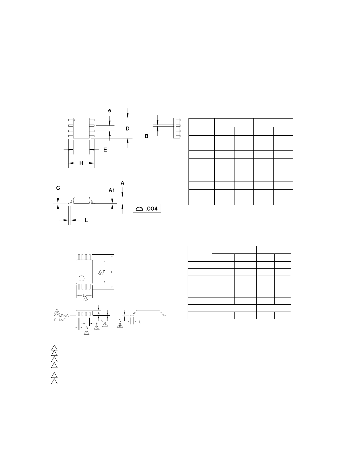
8-Pin SOIC Narrow (SN)
bq2057
TS: 8-Pin TSSOP
8-Pin SN(0.150" SOIC
Inches Millimeters
Dimension
A 0.060 0.070 1.52 1.78
A1 0.004 0.010 0.10 0.25
B 0.013 0.020 0.33 0.51
C 0.007 0.010 0.18 0.25
D 0.185 0.200 4.70 5.08
E 0.150 0.160 3.81 4.06
e 0.045 0.055 1.14 1.40
H 0.225 0.245 5.72 6.22
L 0.015 0.035 0.38 0.89
Dimension
A - 0.043 - 1.10
A1 0.002 0.006 0.05 0.15
B 0.007 0.012 0.18 0.30
C 0.004 0.007 0.09 0.18
D 0.1 14 0.122 2.90 3.10
E 0.169 0.176 4.30 4.48
e 0.0256BSC 0.65BSC
H 0.246 0.256 6.25 6.50
Min. Max. Min. Max.
Inches Millimeters
Min. Max. Min. Max.
)
Notes:
1. Controlling dimension: millimeters. Inches shown for reference only.
2 'D' and 'E' do not include mold flash or protrusions. Mold flash or protrusions shall not exceed 0.15mm per side
3 Each lead centerline shall be located within ±0.10mm of its exact true position.
4. Leads shall be coplanar within 0.08mm at the seating plane.
5 Dimension 'B' does not include dambar protrusion. The dambar protrusion(s) shall not cause the lead width
to exceed 'B' maximum by more than 0.08mm.
6 Dimension applies to the flat section of the lead between 0.10mm and 0.25mm from the lead tip.
7 'A1' is defined as the distance from the seating plane to the lowest point of the package body (base plane).
11
Page 12

IMPORTANT NOTICE
T exas Instruments and its subsidiaries (TI) reserve the right to make changes to their products or to discontinue
any product or service without notice, and advise customers to obtain the latest version of relevant information
to verify, before placing orders, that information being relied on is current and complete. All products are sold
subject to the terms and conditions of sale supplied at the time of order acknowledgment, including those
pertaining to warranty, patent infringement, and limitation of liability.
TI warrants performance of its semiconductor products to the specifications applicable at the time of sale in
accordance with TI’s standard warranty. Testing and other quality control techniques are utilized to the extent
TI deems necessary to support this warranty . Specific testing of all parameters of each device is not necessarily
performed, except those mandated by government requirements.
Customers are responsible for their applications using TI components.
In order to minimize risks associated with the customer’s applications, adequate design and operating
safeguards must be provided by the customer to minimize inherent or procedural hazards.
TI assumes no liability for applications assistance or customer product design. TI does not warrant or represent
that any license, either express or implied, is granted under any patent right, copyright, mask work right, or other
intellectual property right of TI covering or relating to any combination, machine, or process in which such
semiconductor products or services might be or are used. TI’s publication of information regarding any third
party’s products or services does not constitute TI’s approval, warranty or endorsement thereof.
Copyright 2000, Texas Instruments Incorporated
 Loading...