

查询BQ2003供应商
bq2003
Fast-Charge IC
Features
Fast charge and conditioning of
➤
nickel cadmium or nickel-metal
hydride batteries
Hysteretic PWM switch-mode
➤
current regulation or gated con
trol of an external regulator
Easily integrated into systems
➤
or used as a stand-alone charger
Pre-charge qualification of tem
➤
perature and voltage
Direct LED outputs display
➤
battery and charge status
Fast-charge termination by
➤
temperature/∆time, -∆V, maxi-
∆
mum voltage, maximum temperature, and maximum time
➤ Optional top-off charge
Pin Connections
CCMD
DCMD
DVEN
TM
TM
BAT
V
1
2
TS
SS
16
1
2
15
3
14
4
13
5
12
6
11
7
10
8
9
V
CC
DIS
MOD
CHG
TEMP
MCV
TCO
SNS
General Description
The bq2003 Fast Charge IC provides
comprehensive fast charge control
functions together with high-speed
switching power control circuitry on a
monolithic CMOS device.
Integration of closed-loop current
control circuitry allows the bq2003
to be the basis of a cost-effective so
lution for stand-alone and systemintegrated chargers for batteries of
one or more cells.
Switch-activated discharge-beforecharge allows bq2003-based chargers
to support battery conditioning and
capacity determination.
High-efficiency power conversion is
accomplished using the bq2003 as a
hysteretic PWM controller for
switch-mode regulation of the charging current. The bq2003 may alternatively be used to gate an externally
regulated charging current.
Pin Names
CCMD Charge command/select
DCMD Discharge command
DVEN -∆V enable/disable
TM
TM
TS Temperature sense
BAT Battery voltage
V
SS
Timer mode select 1
1
Timer mode select 2
2
System ground
Fast charge may begin on applica
tion of the charging supply, replace
ment of the battery, or switch de
pression. For safety, fast charge is
inhibited unless/until the battery
temperature and voltage are within
configured limits.
Temperature, voltage, and time are
monitored throughout fast charge.
-
Fast charge is terminated by any of
the following:
Rate of temperature rise
n
(∆T/∆t)
Negative delta voltage (-∆V)
n
Maximum voltage
n
Maximum temperature
n
Maximum time
n
After fast charge, an optional top-off
phase is available. Constant-current maintenence charge is provided
by an external trickle resistor.
SNS Sense resistor input
TCO Temperature cutoff
MCV Maximum voltage
TEMP Temperature status
output
CHG Charging status output
MOD Charge current control
DIS Discharge control
V
CC
5.0V±10% power
-
-
-
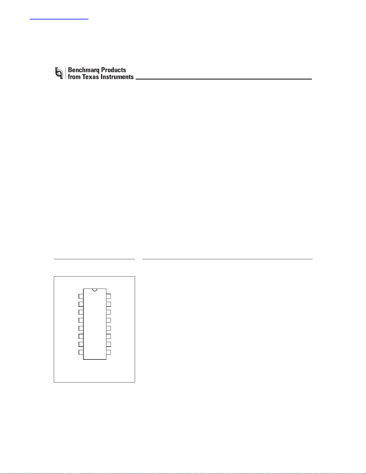
16-Pin DIP or SOIC
PN200301.eps
SLUS095A - OCTOBER 1999 I
1

bq2003
Pin Descriptions
CCMD,
DCMD
DVEN
TM
TM
TS
BAT
Vss
SNS
Charge initiation and discharge-beforecharge control inputs
These two inputs control the conditions that
begin a new charge cycle and enable
discharge-before-charge. See Table 1.
-∆V enable input
This input enales/disables -∆V charge termina
tion. If DVEN is high, the -∆V test is enabled.
If DVEN is low, -∆V test is disabled. The state
of DVEN may be changed at any time.
Timer mode inputs
–
1
2
TM
and TM2are three-state inputs that con
1
figure the fast charge safety timer, -∆V holdoff time, and that enhance/disable top-off.
See Table 2.
Temperature sense input
Input, referenced to SNS, for an external
thermistor monitoring battery temperature.
Single-cell voltage input
The battery voltage sense input, referenced
to SNS. This is created by a high-impedance
resistor divider network connected between
the positive and the negative terminals of
the battery.
Ground
Charging current sense input
SNS controls the switching of MOD based on
the voltage across an external sense resistor
in the current path of the battery. SNS is the
reference potential for the TS and BAT pins.
If SNS is connected to V
high at the beginning of charge and low at
the end of charge.
, MOD switches
SS
-
-
TCO
MCV
TEMP
CHG
MOD
DIS
V
CC
Temperature cutoff threshold input
Input to set maximum allowable battery
temperature. If the potential between TS
and SNS is less than the voltage at the TCO
input, then fast charge or top-off charge is
terminated.
Maximum-Cell-Voltage threshold input
Input to set maximum single-cell equivalent
voltage. If the voltage between BAT and SNS
is greater than or equal to the voltage at the
MCV input, then fast charge or top-off charge
is inhibited.
Note: For valid device operation, the
voltage level on MCV must not exceed
0.6 ∗ V
CC
.
Temperature status output
Push-pull output indicating temperature
status. TEMP is low if the voltage at the TS
pin is not within the allowed range to start
fast charge.
Charging status output
Push-pull output indicating charging status.
See Figure 1.
Current-switching control output
MOD is a push/pull output that is used to
control the charging current to the battery.
MOD switches high to enable charging cur
rent flow and low to inhibit charging current
flow.
Discharge FET control output
Push-pull output used to control an external
transistor to discharge the battery before
charging.
VCCsupply input
5.0 V, ±10% power input.
-
2
bq2003
Functional Description
Figure 3 shows a state diagram and Figure 4 shows a
block diagram of the bq2003.
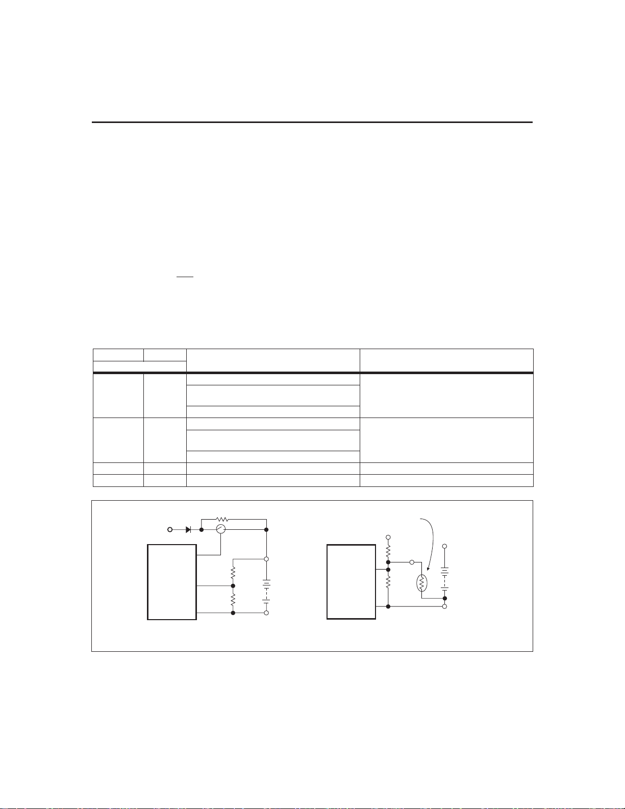
Battery Voltage and Temperature
Measurements
Battery voltage and temperature are monitored for
maximum allowable values. The voltage presented on
the battery sense input, BAT, should represent a
single-cell potential for the battery under charge. A
resistor-divider ratio of:
RB1
= N - 1
RB2
is recommended to maintain the battery voltage within
the valid range, where N is the number of cells, RB1 is
Table 1. New Charge Cycle and Discharge Stimulus
CCMD DCMD New Charge Cycle
Pulled Up/Down to:
V
SS
V
CC
V
SS
V
CC
(V
(V
A falling edge on CCMD or DCMD
V
CC
V
SS
V
SS
V
CC
Started by:
VCCrising to valid level
Battery replacement
falling through V
CELL
A rising edge on CCMD
VCCrising to valid level
Battery replacement
falling through V
CELL
A rising edge on CCMD A rising edge on DCMD
A falling edge on CCMD A rising edge on DCMD
the resistor connected to the positive battery terminal,
and RB2 is the resistor connected to the negative bat
tery terminal. See Figure 1.
Note: This resistor-divider network input impedance to
end-to-end should be at least 200kΩ and less than 1MΩ.
A ground-referenced negative temperature coefficient
thermistor placed in proximity to the battery may be used
as a low-cost temperature-to-voltage transducer. The tem
perature sense voltage input at TS is developed using a re
sistor-thermistor network between V
and battery’s nega
CC
tive terminal See Figure 1. Both the BAT and TS inputs
are referenced to SNS, so the signals used inside the IC are:
V
BAT-VSNS=VCELL
and
V
TS-VSNS=VTEMP
Discharge-Before-Charge
Started by:
MCV
MCV
)
)
A rising edge on DCMD
A rising edge on DCMD
-
-
-
-
V
DC
bq2003
External Trickle Resistor Negative Temperature
Pass Element
MOD
RB1
BAT
RB2
SNS
PACK+
PACK-
Coefficient Thermister
T
S
bq2003
SNS
V
CC
RT1
RT2
PACK +
N
T
C
PACK -
Fg2003a2.eps
Figure 1. Voltage and Temperature Monitoring and Trickle Resistor
3
bq2003
Discharge-Before-Charge
The DCMD input is used to command discharge-beforecharge via the DIS output. Once activated, DIS becomes
active (high) until V
falls below V
CELL
at which time
EDV,
DIS goes low and a new fast charge cycle begins. See
Table 1 for the conditions that initiate discharge-beforecharge. Discharge-before-charge is qualified by the
same voltage and temperature conditions that qualify a
new charge cycle start (see below). If a discharge is ini
tiated but the pack voltage or temperature is out of
range, the chip enters the charge pending mode and
trickle charges the battery until the voltage and tem
perature qualification conditions are met, and then
starts to discharge.
Starting A Charge Cycle
The stimulus required to start a new charge cycle is de
termined by the configuration of the CCMD and DCMD
inputs. If CCMD and DCMD are both pulled up or
pulled down, then a new charge cycle is started by (see
Figure 2):
1. V
2. V
rising above 4.5V
CC
falling through the maximum cell voltage,
CELL
V
MCV
.V
is the voltage presented at the MCV
MCV
input pin, and is configured by the user with a resistor divider between V
lowed range is 0.2 to 0.4 ∗ V
and ground. The al-
CC
.
CC
3. A rising edge on CCMD if it is pulled down, or a fal
ling edge on CCMD if it is pulled up.
Starting a new charge cycle may be limited to a pushbutton or logical pulse input only by pulling one member
of the DCMD and CCMD pair up while pulling the other
input down. In this configuration a new charge cycle
will be started only by a falling edge on CCMD if it is
pulled up, and by a falling edge on CCMD if it is pulled
down. See Table 1.
-
If the battery is within the configured temperature and
voltage limits, the IC begins fast charge. The valid bat
tery voltage range is V
EDV<VBAT<VMCV
= 0.2 ∗ VCC± 30mV
V
EDV
The valid temperature range is V
where:
HTF<VTEMP<VLTF
where:
-
= [(1/8 ∗ V
V
HTF
V
is the voltage presented at the TCO input pin, and is
TCO
= 0.4 ∗ VCC± 30mV
V
LTF
) + (7/8 ∗ V
LTF
)] ± 30mV
TCO
configured by the user with a resistor divider between V
and ground. The allowed range is 0.2 to 0.4 ∗ VCC.
If the temperature of the battery is out of range, or the
voltage is too low, the chip enters the charge pending
state and waits for both conditions to fall within their
allowed limits. There is no time limit on the charge
pending state; the charger remains in this state as long
as the voltage or temperature conditons are outside of
-
-
,
CC
Charge
Pending
DIS
MOD Switch-Mode Configuration
or
MOD External Regulation
(SNS Grounded)
CHG Status Output
TEMP Status Output
Charge cycle start.
Battery outside temperature limits.
Discharge
(Optional)
Battery discharged to 0.2 VCC.
Battery within temperature limits.
Fast Charging Top-Off
Figure 2. Charge Cycle Phases
4
sec
4
(Optional)
.
34 sec.
TD200301a.eps

Table 2. Fast-Charge Safety Time/Hold-Off/Top-Off Table
Corresponding
Fast-Charge Rate TM1 TM2
C/4 Low Low 360 137 Disabled
C/2 Float Low 180 820 Disabled
1C High Low 90 410 Disabled
2C Low Float 45 200 Disabled
4C Float Float 23 100 Disabled
C/2 High Float 180 820 C/16
1C Low High 90 410 C/8
2C Float High 45 200 C/4
4C High High 23 100 C/2
Note: Typical conditions = 25°C, VCC= 5.0V.
the allowed limits. If the voltage is too high, the chip
goes to the battery absent state and waits until a new
charge cycle is started.
Fast charge continues until termination by one or more
of the five possible termination conditions:
Delta temperature/delta time (∆T/∆t)
n
n Negative delta voltage (-
n
Maximum voltage
n
Maximum temperature
n
Maximum time
V)
∆
-∆V Termination
If the DVEN input is high, the bq2003 samples the volt
age at the BAT pin once every 34s. If V
CELL
is lower
than any previously measured value by 12mV ±4mV,
fast charge is terminated. The -∆V test is valid in the
range V
- (0.2 ∗ VCC)<V
MCV
CELL<VMCV
.
Voltage Sampling
Each sample is an average of 16 voltage measurements
taken 57µs apart. The resulting sample period (18.18ms)
filters out harmonics around 55Hz. This technique mini
mizes the effect of any AC line ripple that may feed
through the power supply from either 50Hz or 60Hz AC
sources. Tolerance on all timing is ±16%.
Voltage Termination Hold-off
A hold-off period occurs at the start of fast charging.
During the hold-off period, -∆V termination is disabled.
This avoids premature termination on the voltage spikes
sometimes produced by older batteries when fast-charge
current is first applied. ∆T/∆t, maximum voltage and
bq2003
Typical Fast Charge
and Top-Off
Time Limits
maximum temperature terminations are not affected by
the hold-off period.
∆T/∆t Termination
The bq2003 samples at the voltage at the TS pin every
34s, and compares it to the value measured two samples
earlier. If V
TEMP
charge is terminated. The ∆T/∆t termination test is
valid only when V
TCO<VTEMP<VLTF
Temperature Sampling
Each sample is an average of 16 voltage measurements
taken 57µs apart. The resulting sample period
(18.18ms) filters out harmonics around 55Hz. This tech
nique minimizes the effect of any AC line ripple that
may feed through the power supply from either 50Hz or
60Hz AC sources. Tolerance on all timing is ±16%.
-
Maximum Voltage, Temperature, and Time
Anytime V
goes off) immediately. If the bq2003 is not in the voltage
hold-off period, fast charging ceases if V
MCV for a minimum of t
low V
MCV
Charge Complete state (maximum voltage termination). If
V
remains above V
CELL
transitions to the Battery Absent state (battery removal).
See Figure 3.
If the bq2003 is in the voltage hold-off period when
V
CELL
charging continues until the expiration of the hold-off
period. Temperature sampling continues during the
hold-off period as well. If a new battery is inserted be
fore the hold-off period expires, it continues in the fast
charge cycle started by its predecessor. No precharge
qualification is performed, and a temperature sample
rises above V
CELL
before 1.5t
rises above V
Typical -∆V/MCV
Hold-Off
Time (seconds)
has fallen 16mV ±4mV or more, fast
.
CHG goes high (the LED
MCV,
remains above
.IfV
MCV
±50ms, the chip transitions to the
MCV
beyond 1.5t
MCV
the LED goes out but fast
MCV,
CELL
then falls back be
CELL
MCV
, the bq2003
Top-Off
Rate
-
-
-
5

bq2003
taken on the new battery is compared to ones taken be
fore the original battery was removed and any that may
have been taken while no battery was present. If the IC
is configured for ∆T/∆t termination, this may result in a
premature fast-charge termination on the newly in
serted battery.
Maximum temperature termination occurs anytime the
voltage on the TS pin falls below the temperature cut-off
threshold V
above the minimum temperature fault threshold, V
Charge is also terminated if V
TCO.
TEMP
rises
LTF,
after fast charge begins.
Maximum charge time is configured using the TM pin.
Time settings are available for corresponding charge
rates of C/4, C/2, 1C, and 2C. Maximum time-out termi
nation is enforced on the fast-charge phase, then reset,
and enforced again on the top-off phase, if selected.
There is no time limit on the trickle-charge phase.
Top-off Charge
An optional top-off charge phase may be selected to
follow fast charge termination for the C/2 through 4C
rates. This phase may be necessary on NiMH or other
battery chemistries that have a tendency to terminate
charge prior to reaching full capacity. With top-off enabled, charging continues at a reduced rate after
fast-charge termination for a period of time selected
by the TM
and TM2input pins. (See Table 2.) During
1
top-off, the MOD pin is enabled at a duty cycle of 4s
active for every 30s inactive. This modulation results
in an average rate 1/8th that of the fast charge rate.
Maximum voltage, time, and temperature are the only
termination methods enabled during top-off.
External Trickle Resistor
Maintenance charging is provided by the use of an exter
nal trickle resistor between the high side of the battery
pack and V
Figure 1.) This resistor is sized to meet two criteria.
n
With the battery removed, the resistor must pull the
voltage at the BAT input above MCV for battery
insertion and removal detection.
n
With the battery at its fully charged voltage, the
trickle current should be approximately equal to the
self-discharge rate of the battery.
, the input charging supply voltage. (See
DC
-
Charge Status Indication
Charge status is indicated by the CHG output. The state
of the CHG output in the various charge cycle phases is
shown in Figure 3 and illustrated in Figure 1.
-
Temperature status is indicated by the TEMP output.
TEMP is in the high state whenever V
temperature window defined by the V
TEMP
LTF
and V
is within the
perature limits, and is low when the battery tempera
ture is outside these limits.
In all cases, if V
exceeds the voltage at the MCV
CELL
pin, both CHG and TEMP outputs are held high regard
less of other conditions. CHG and TEMP may both be used
to directly drive an LED.
-
Charge Current Control
The bq2003 controls charge current through the MOD
output pin. The current control circuitry is designed to
support implementation of a constant-current switching
regulator or to gate an externally regulated current
source.
When used in switch-mode configuration, the nominal
regulated current is:
I
= 0.235V/R
REG
Charge current is monitored at the SNS input by the
voltage drop across a sense resistor, R
low side of the battery pack and ground. R
provide the desired fast-charge current.
If the voltage at the SNS pin is less than V
MOD output is switched high to pass charge current to
the battery.
When the SNS voltage is greater than V
output is switched low—shutting off charging current to
the battery.
V
= 0.044 ∗ VCC± 25mV
SNSLO
= 0.05 ∗ VCC± 25mV
V
SNSHI
When used to gate an externally regulated current
source, the SNS pin is connected to V
sisitor is required.
SNS
, between the
SNS
SNS
SNSHI
, and no sense re
SS
SNSLO
, the MOD
tem
HTF
is sized to
, the
-
-
-
-
6

V
EDV
New Charge Cycle Start or
Discharge-Before-Charge
Command
Battery Voltage?
< V
< V
CELL
MCV
Temperature?
No
Discharge-Before-Charge
Commanced?
Battery
V
HTF
V
V
< V
TEMP
TEMP
TEMP
V
V
CELL
CELL
> V
< V
< V
> V
< V
LTF
HTF
LTF
MCV
EDF
or
Trickle
CHG =
1 3/8s high
1/8s low
V
and
V
Charge
Pending
< V
EDV
< V
HTF
V
CELL
CELL
TEMP
> V
< V
< V
bq2003
MCV
MCV
LTF
- V or
T/ t or
V
TEMP
or
Maximum
Time Out
<
Discharge
CHG =
1 3/8s low
1/8s high
Fast
CHG =
Low
V
TCO
Top-off
selected?
No
V
CELL
V
EDV
<
V
> V
CELL
MCV
V
>
CELL
V
Yes
MCV
V
CELL
V
MCV
<
Hold-off
period
expired?
Fast
CHG =
High
No
Figure 3. State Diagram
Yes
Hold-off
period
expires
V
V
Top-off
CHG =
1/8s low
1/8s high
V
CELL
CELL
MCV
Trickle
CHG =
High
<
V
MCV
>
V
TEMP
or Maximum
Time Out
t > 1.5t
V
V
< V
TCO
Battery
Absent
MCV
CELL
MCV
>
1/8s low
1/8s high
Trickle
CHG =
High
Trickle
CHG =
SD2003.eps
Charge
Complete
7

bq2003
TCOTM2TM1
TEMP
CHG
CCMD
DCMD
DVEN
- V
SNS
SNS
TCO
Check
LTF
Check
A/D
EDV
OSC
Display
Control
Charge Control
State Machine
Timing
Control
VTS - V
V
BAT
Check
Discharge
Control
MOD
Control
MCV
Check
DIS MOD MCV VCCV
BD200301.eps
Figure 4. Block Diagram
TS
SNS
BAT
SS
8

bq2003
Absolute Maximum Ratings
Symbol Parameter Minimum Maximum Unit Notes
V
CC
V
T
T
OPR
T
STG
T
SOLDER
T
BIAS
VCCrelative to V
DC voltage applied on any pin ex
cluding V
CC
SS
relative to V
SS
-
Operating ambient temperature 0 +70 °C Commercial
Storage temperature -55 +125 °C
Soldering temperature - +260 °C 10 sec max.
Temperature under bias -40 +85 °C
Note: Permanent device damage may occur if Absolute Maximum Ratings are exceeded. Functional opera
tion should be limited to the Recommended DC Operating Conditions detailed in this data sheet. Expo
sure to conditions beyond the operational limits for extended periods of time may affect device reliability.
-0.3 +7.0 V
-0.3 +7.0 V
-
-
DC Thresholds (T
A=TOPR;VCC
10%)
±
Symbol Parameter Rating Tolerance Unit Notes
-
-
(1/8 ∗ V
0.05 ∗ V
0.044 ∗ V
0.4 ∗ V
) + (7/8 ∗ V
LTF
0.2 ∗ V
-16
-12
CC
CC
CC
CC
TCO
0.025
±
0.025
±
0.030
±
)
0.030
±
0.030
±
±4
±4
Tolerance is common
V
mode deviation.
Tolerance is common
V
mode deviation.
V
TEMP
V
terminates charge
V
TEMP
V
fast charge
V
CELL<VEDV
V
fast charge
V
mV
mV
CC
V
CC
V
≥
LTF
V
≤
HTF
= 5V, TA= 25°C
= 5V, TA= 25°C
V
SNSHI
V
SNSLO
V
LTF
V
HTF
V
EDV
V
THERM
-∆V
High threshold at SNS re
sulting in MOD = Low
Low threshold at SNS re
sulting in MOD = High
Low-temperature fault
High-temperature fault
End-of-discharge voltage
TS input change for
∆T/∆t detection
BAT input change for
-∆V detection
9
inhibits/
inhibits
inhibits

bq2003
Recommended DC Operating Conditions (T
= 0 to +70°C)
A
Symbol Parameter Minimum Typical Maximum Unit Notes
V
V
V
V
V
V
V
V
V
V
V
I
CC
I
OH
I
OL
I
IL
I
IH
I
IZ
CC
BAT
CELL
TS
TEMP
MCV
TCO
IH
IL
OH
OL
Supply voltage 4.5 5.0 5.5 V
Battery input 0 - V
BAT voltage potential 0 - V
Thermistor input 0 - V
TS voltage potential 0 - V
Maximum cell voltage
Temperature cutoff
0.2 ∗ V
0.2 ∗ V
CC
CC
-
0.4 ∗ V
-
0.4 ∗ V
CC
CC
CC
CC
CC
CC
V
VV
BAT
V
VVTS- V
V
V
- V
SNS
SNS
Logic input high VCC- 1.0 - - V CCMD, DCMD, DVEN
Logic input high V
- 0.3 - - V TM1,TM
CC
2
Logic input low - - 1.0 V CCMD, DCMD, DVEN
Logic input low - - 0.3 V TM
V
Logic output high
CC
- 0.5
--V
Logic output low - - 0.5 V
,TM
1
2
DIS, TEMP, CHG, MOD,
-5mA
I
≤
OH
DIS, TEMP, CHG, MOD,
I
5mA
≤
OL
Supply current - 0.75 2.2 mA Outputs unloaded
DIS, TEMP, MOD, CHG source -5.0 - - mA @VOH= VCC- 0.5V
DIS, TEMP, MOD, CHG sink 5.0 - - mA @VOL= VSS+ 0.5V
CCMD, DCMD, DVEN,
A
Input leakage - -
±
Logic input low source - - 70
Logic input high source -70 - -
TM1,TM2tri-state open
detection
-2.0 - 2.0
1
µ
V = V
TM
A
µ
V = V
TM
A
µ
V = V
TM
A
µ
connected (floating) for Z
to V
SS
,TM2,
1
to VSS+ 0.3V
SS
,TM2,
1
- 0.3V to V
CC
,TM2may be left dis
1
logic input state
CC
CC
-
Note: All voltages relative to VSSexcept as noted.
10

bq2003
Impedance
Symbol Parameter Minimum Typical Maximum Unit
R
R
R
R
R
BAT
MCV
TCO
SNS
TS
Battery input impedance 50 - - M
MCV input impedance 50 - - M
TCO input impedance 50 - - M
SNS input impedance 50 - - M
TS input impedance 50 - - M
Ω
Ω
Ω
Ω
Ω
Timing (T
= 0 to +70°C; V
A
CC
10%)
±
Symbol Parameter Minimum Typical Maximum Unit Notes
t
PW
d
f
REG
t
MCV
FCV
Pulse width for CCMD,
DCMD pulse commands
1- -
Time base variation -16 - 16 % VCC= 4.5V to 5.5V
MOD output regulation
frequency
Maximum voltage
termination time limit
- - 300 kHz
200 250 300 ms
Pulse start for charge or discharge-
s
µ
before-charge
Time limit to distinguish battery re
moved from charge complete
Note: Typical is at TA= 25°C, VCC= 5.0V.
-
11

bq2003
PN: 16-Pin DIP Narrow
S: 16-Pin SOIC
16-Pin PN(DIP Narrow
)
Dimension Minimum Maximum
A 0.160 0.180
A1 0.015 0.040
B 0.015 0.022
B1 0.055 0.065
C 0.008 0.013
D 0.740 0.770
E 0.300 0.325
E1 0.230 0.280
e 0.300 0.370
G 0.090 0.110
L 0.115 0.150
S 0.020 0.040
All dimensions are in inches.
16-Pin S(SOIC
)
Dimension Minimum Maximum
D
e
B
A 0.095 0.105
A1 0.004 0.012
B 0.013 0.020
C 0.008 0.013
E
H
D 0.400 0.415
E 0.290 0.305
e 0.045 0.055
A
C
L
A1
.004
H 0.395 0.415
L 0.020 0.040
All dimensions are in inches.
12

bq2003
Data Sheet Revision History
Change No. Page No. Description Nature of Change
5 2 Changed block diagram Changed diagram.
5 8 Added top-off values to Table 2. Added values.
6 All Revised and expanded format of this data sheet Clarification
79
8 3 Corrected Table 1 Correction
85,7
T
OPR
Corrected and expanded the explanation for maxi
mum voltage conditions
Deleted industrial temperature
range.
Clarification
Notes: Changes 1–4: Please refer to the 1997 Data Book.
Change 5 = Sept. 1996 F changes from Oct. 1993 E.
Change 6 = Oct. 1997 G changes from Sept. 1996 F.
Change 7 = June 1999 H changes from Oct. 1997 G.
Change 8 = Oct. 1999 I changes from June 1999 H.
Ordering Information
bq2003
Package Option:
PN = 16-pin narrow plastic DIP
S = 16-pin SOIC
Device:
bq2003 Fast-Charge IC
13

PACKAGE OPTION ADDENDUM
www.ti.com
2-May-2005
PACKAGING INFORMATION
Orderable Device Status
(1)
Package
Type
Package
Drawing
Pins Package
Qty
Eco Plan
BQ2003PN ACTIVE PDIP N 16 25 TBD Call TI Level-NA-NA-NA
BQ2003PN-N ACTIVE PDIP N 16 25 TBD Call TI Level-NA-NA-NA
BQ2003S ACTIVE SOIC DW 16 40 TBD Call TI Level-2-220C-1 YEAR
BQ2003S-N ACTIVE SOIC DW 16 46 TBD Call TI Level-2-220C-1 YEAR
BQ2003S-NTR ACTIVE SOIC DW 16 2000 TBD Call TI Level-2-220C-1 YEAR
BQ2003STR ACTIVE SOIC DW 16 2000 TBD Call TI Level-2-220C-1 YEAR
(1)
The marketing status values are defined as follows:
ACTIVE: Product device recommended for new designs.
LIFEBUY: TI has announced that the device will be discontinued, and a lifetime-buy period is in effect.
NRND: Not recommended for new designs. Device is in production to support existing customers, but TI does not recommend using this part in
a new design.
PREVIEW: Device has been announced but is not in production. Samples may or may not be available.
OBSOLETE: TI has discontinued the production of the device.
(2)
Eco Plan - The planned eco-friendly classification: Pb-Free (RoHS) or Green (RoHS & no Sb/Br) - please check
http://www.ti.com/productcontent for the latest availability information and additional product content details.
TBD: The Pb-Free/Green conversion plan has not been defined.
Pb-Free (RoHS): TI's terms "Lead-Free" or "Pb-Free" mean semiconductor products that are compatible with the current RoHS requirements
for all 6 substances, including the requirement that lead not exceed 0.1% by weight in homogeneous materials. Where designed to be soldered
at high temperatures, TI Pb-Free products are suitable for use in specified lead-free processes.
Green (RoHS & no Sb/Br): TI defines "Green" to mean Pb-Free (RoHS compatible), and free of Bromine (Br) and Antimony (Sb) based flame
retardants (Br or Sb do not exceed 0.1% by weight in homogeneous material)
(2)
Lead/Ball Finish MSL Peak Temp
(3)
(3)
MSL, Peak Temp. -- The Moisture Sensitivity Level rating according to the JEDEC industry standard classifications, and peak solder
temperature.
Important Information and Disclaimer:The information provided on this page represents TI's knowledge and belief as of the date that it is
provided. TI bases its knowledge and belief on information provided by third parties, and makes no representation or warranty as to the
accuracy of such information. Efforts are underway to better integrate information from third parties. TI has taken and continues to take
reasonable steps to provide representative and accurate information but may not have conducted destructive testing or chemical analysis on
incoming materials and chemicals. TI and TI suppliers consider certain information to be proprietary, and thus CAS numbers and other limited
information may not be available for release.
In no event shall TI's liability arising out of such information exceed the total purchase price of the TI part(s) at issue in this document sold by TI
to Customer on an annual basis.
Addendum-Page 1

IMPORTANT NOTICE
Texas Instruments Incorporated and its subsidiaries (TI) reserve the right to make corrections, modifications,
enhancements, improvements, and other changes to its products and services at any time and to discontinue
any product or service without notice. Customers should obtain the latest relevant information before placing
orders and should verify that such information is current and complete. All products are sold subject to TI’s terms
and conditions of sale supplied at the time of order acknowledgment.
TI warrants performance of its hardware products to the specifications applicable at the time of sale in
accordance with TI’s standard warranty. Testing and other quality control techniques are used to the extent TI
deems necessary to support this warranty . Except where mandated by government requirements, testing of all
parameters of each product is not necessarily performed.
TI assumes no liability for applications assistance or customer product design. Customers are responsible for
their products and applications using TI components. To minimize the risks associated with customer products
and applications, customers should provide adequate design and operating safeguards.
TI does not warrant or represent that any license, either express or implied, is granted under any TI patent right,
copyright, mask work right, or other TI intellectual property right relating to any combination, machine, or process
in which TI products or services are used. Information published by TI regarding third-party products or services
does not constitute a license from TI to use such products or services or a warranty or endorsement thereof.
Use of such information may require a license from a third party under the patents or other intellectual property
of the third party, or a license from TI under the patents or other intellectual property of TI.
Reproduction of information in TI data books or data sheets is permissible only if reproduction is without
alteration and is accompanied by all associated warranties, conditions, limitations, and notices. Reproduction
of this information with alteration is an unfair and deceptive business practice. TI is not responsible or liable for
such altered documentation.
Resale of TI products or services with statements different from or beyond the parameters stated by TI for that
product or service voids all express and any implied warranties for the associated TI product or service and
is an unfair and deceptive business practice. TI is not responsible or liable for any such statements.
Following are URLs where you can obtain information on other Texas Instruments products and application
solutions:
Products Applications
Amplifiers amplifier.ti.com Audio www.ti.com/audio
Data Converters dataconverter.ti.com Automotive www.ti.com/automotive
DSP dsp.ti.com Broadband www.ti.com/broadband
Interface interface.ti.com Digital Control www.ti.com/digitalcontrol
Logic logic.ti.com Military www.ti.com/military
Power Mgmt power.ti.com Optical Networking www.ti.com/opticalnetwork
Microcontrollers microcontroller.ti.com Security www.ti.com/security
Telephony www.ti.com/telephony
Video & Imaging www.ti.com/video
Wireless www.ti.com/wireless
Mailing Address: Texas Instruments
Post Office Box 655303 Dallas, Texas 75265
Copyright 2005, Texas Instruments Incorporated
 Loading...