

Page 1
bq2002D/T
NiCd/NiMH Fast-Charge Management ICs
Features
Fast charge of nickel cadmium
➤
or nickel-metal hydride batter
ies
Direct LED output displays
➤
charge status
Fast-charge termination by
➤
rate of rise of temperature,
maximum voltage, maximum
temperature, and maximum
time
Internal band-gap voltage ref
➤
erence
Optional top-off charge (bq2002T
➤
only)
➤ Selectable pulse-trickle charge
rates (bq2002T only)
➤ Low-power mode
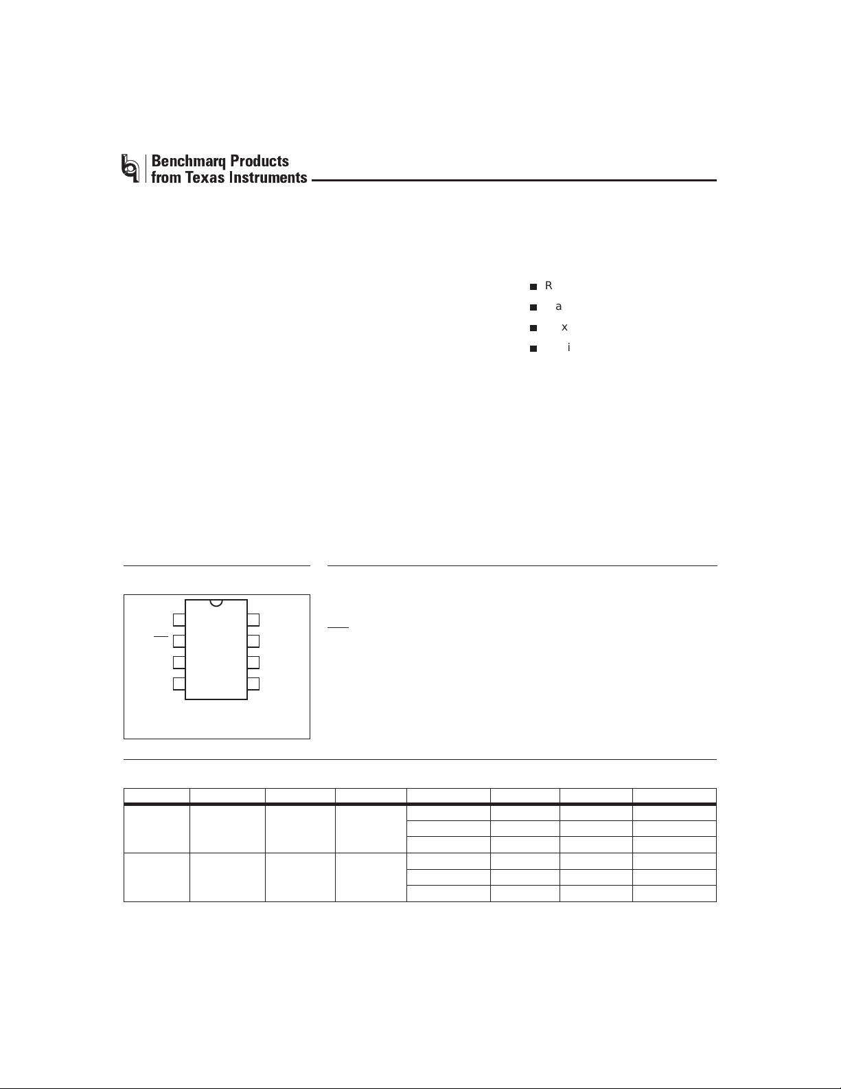
➤ 8-pin 300-mil DIP or 150-mil
SOIC
Pin Connections
TM
LED
BAT
V
1
2
3
4
SS
8
CC
7
INH
V
6
CC
TS
5
General Description
The bq2002D/T Fast-Charge IC are
low-cost CMOS battery-chargecontrol
lers able to provide reliable charge ter
mination for both NiCd and NiMH bat
tery applications. Controlling a
current-limited or constant-current
supply allows the bq2002D/T to be the
basis for a cost-effective stand-alone or
system-integrated charger. The
bq2002D/T integrates fast charge with
optional top-off and pulsed-trickle con
trol in a single IC for charging one or
-
more NiCd or NiMH battery cells.
Fast charge is initiated on application
of the charging supply or battery re
placement. For safety, fast charge is
inhibited if the battery temperature
and voltage are outside configured
limits.
Pin Names
TM Timer mode select input
LED
BAT Battery voltage input
V
SS
Charging status output
System ground
Fast charge is terminated by any of
the following:
Rate of temperature rise
n
-
-
Maximum voltage
n
Maximum temperature
n
Maximum time
n
After fast charge, the bq2002T option
ally tops-off and pulse-trickles the
battery per the pre-configured limits.
-
Fast charge may be inhibited using
the INH pin. The bq2002D/T may be
placed in low-standby-power mode to
reduce system power consumption.
-
TS Temperature sense input
V
CC
Supply voltage input
INH Charge inhibit input
CC Charge control output
-
8-Pin DIP or
Narrow SOIC
PN-200201.eps
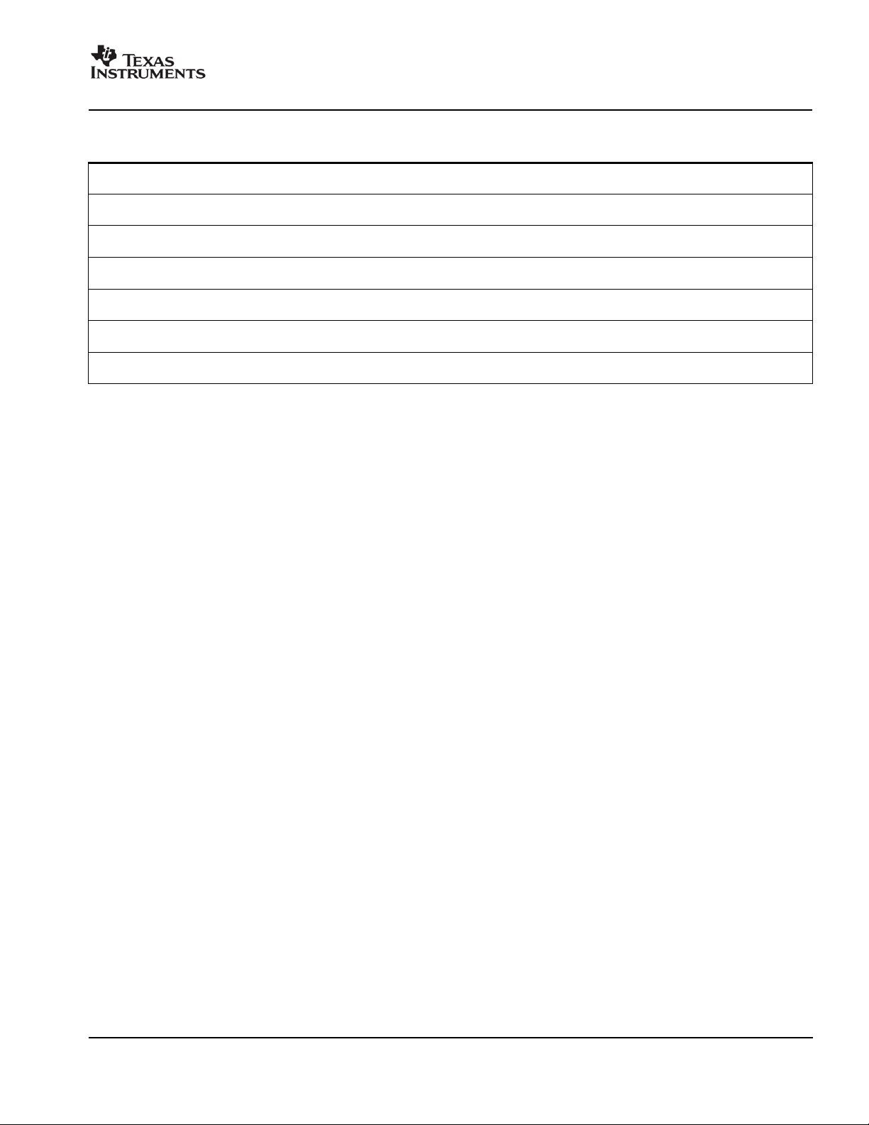
bq2002D/T Selection Guide
Part No. TCO HTF LTF Fast Charge Time-Out Top-Off Maintenance
C/4 440 min None None
bq2002D
bq2002T
SLUS133B–JULY 2000
0.225 ∗ V
0.225 ∗ V
CC
CC
0.25 ∗ V
0.25 ∗ V
CC
CC
None
0.4 ∗ V
CC
1C 110 min None None
2C 55 min None None
C/4 320 min C/64 C/256
1C 80 min C/16 C/256
2C 40 min None C/128
1
Page 2
bq2002D/T
Pin Descriptions
TM
LED
BAT
V
SS
TS
V
CC
INH
Timer mode input
A three-level input that controls the settings
for the fast charge safety timer, voltage ter
mination mode, top-off, pulse-trickle, and
voltage hold-off time.
Charging output status
Open-drain output that indicates the charging
status.
Battery input voltage
The battery voltage sense input. The input
to this pin is created by a high-impedance re
sistor divider network connected between
the positive and negative terminals of the
battery.
System ground
T emperaturesenseinput
Input for an external battery temperature
monitoring thermistor.
Supply voltage input
5.0V±20% power input.
Charge inhibit input
When high, INH suspends the fast charge in
progress. When returned low, the IC re
sumes operation at the point where initially
suspended.
CC
-
Charge control output
An open-drain output used to control the
charging current to the battery. CC switch
ing to high impedance (Z) enables charging
current to flow, and low to inhibit charging
current. CC is modulated to provide top-off,
if enabled, and pulse trickle.
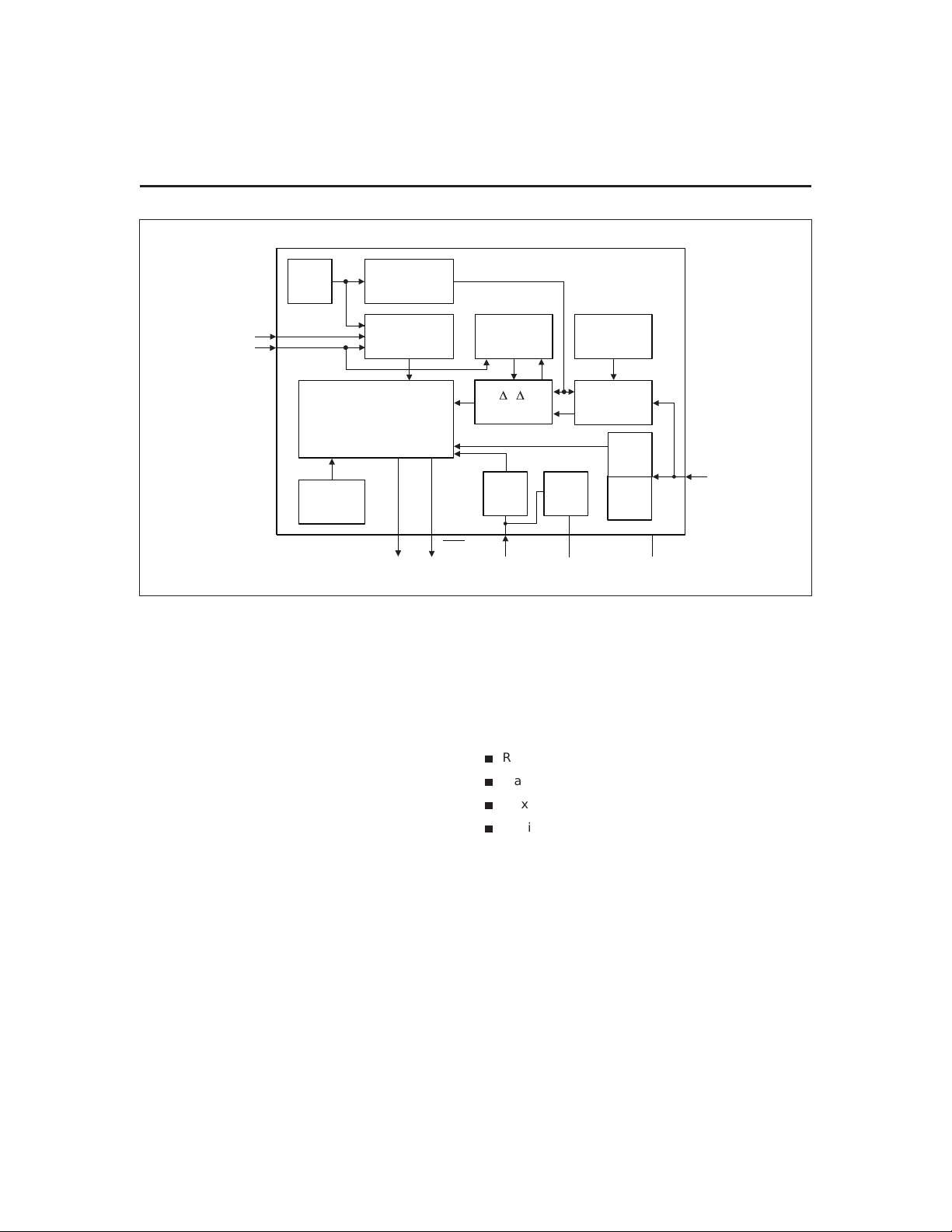
Functional Description
Figures 2 and 3 show state diagrams of bq2002D/T and
Figure 4 shows the block diagram of the bq2002D/T.
-
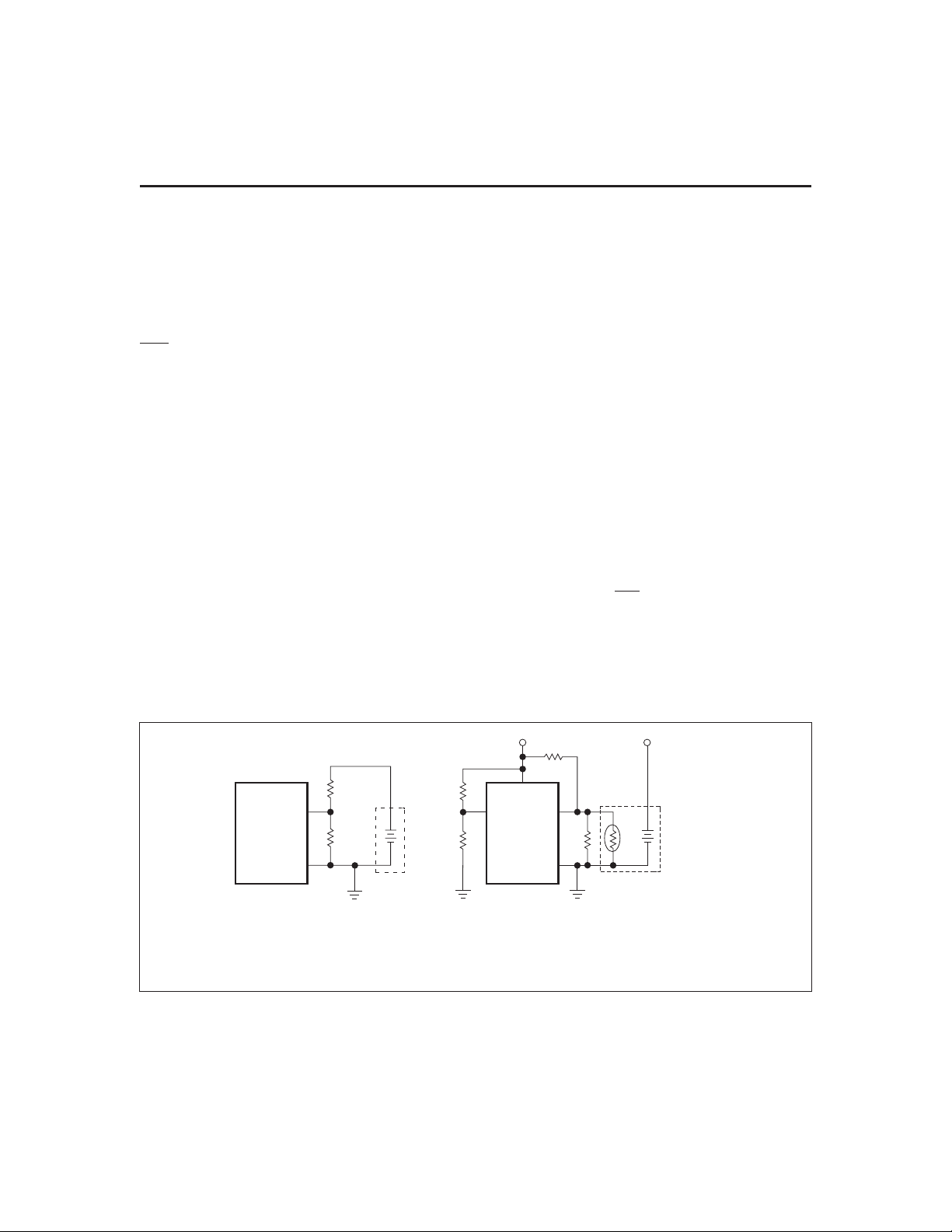
Battery Voltageand Temperature
Measurements
Battery voltage and temperature are monitored for
maximum allowable values. The voltage presented on
the battery sense input, BAT, should represent a
single-cell potential for the battery under charge. A
resistor-dividerratioof
RB1
=N-1
RB2
is recommended to maintain the battery voltage within
the valid range, where N is the number of cells, RB1 is
the resistor connected to the positive battery terminal,
and RB2 is the resistor connected to the negative battery terminal. See Figure 1.
-
-
V
CC
RT1
RB1
BAT
bq2002D/T
V
SS
RB2
BAT pin connection Thermistor connection
R3
R4
Mid-level
V
CC
TM
T
bq2002D/T
V
SS
S
RT2
PACK +
N
T
C
setting for TM
NTC = negative temperature coefficient thermistor.
F2002DT1.eps
Figure 1. Voltage and Temperature Monitoring and TM Pin Configuration
2
Page 3
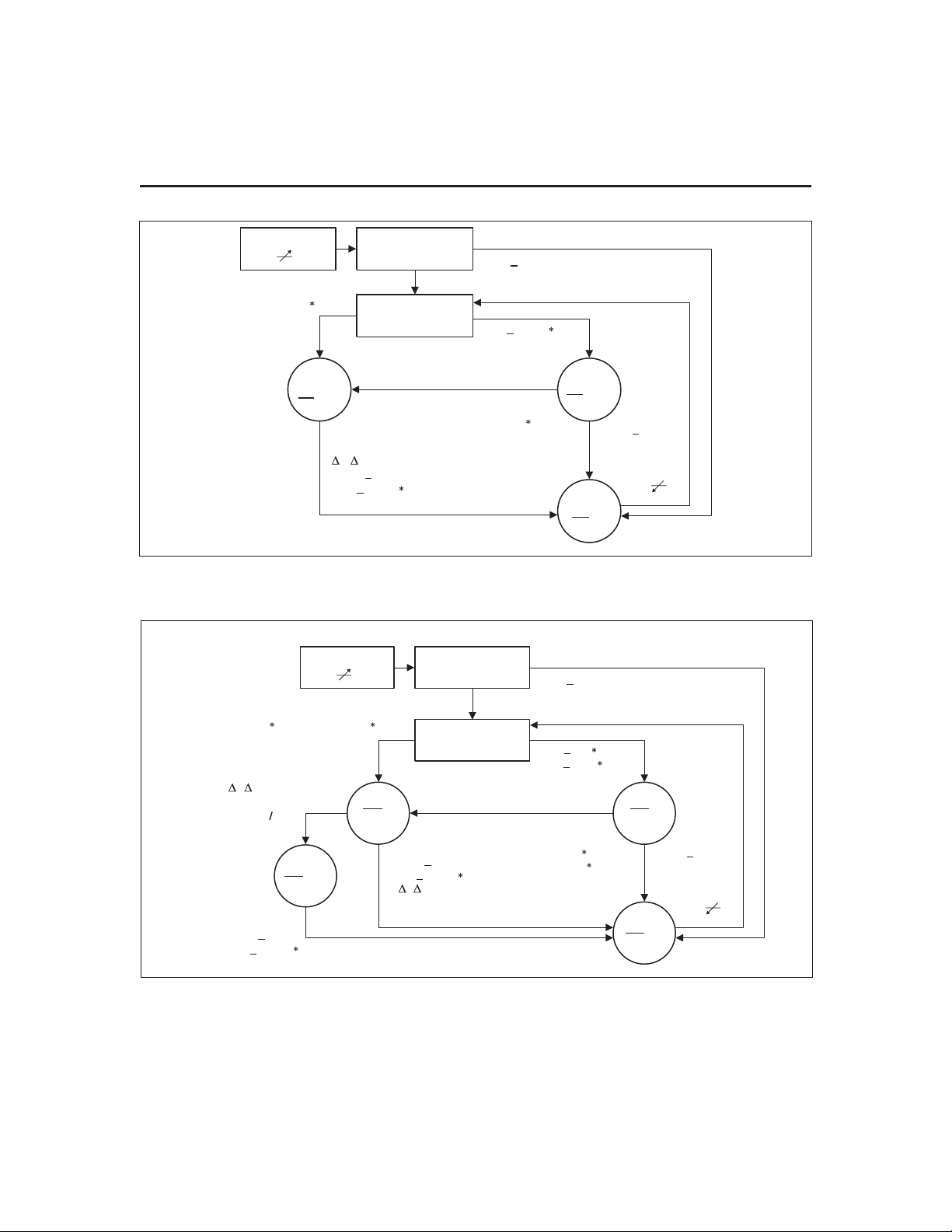
bq2002D/T
Chip on
4.0V
V
CC
Fast Charge,
CC = Z
LED = Low
V
Top-off
LED = Z
V
CC
Chip on
CC
> 0.25V
V
TS
0.25 VCC < VTS < 0.6 V
( T/ t or
Maximum Time Out)
and TM = High
V
> 2V or
BAT
VTS < 0.225 VCC or
Maximum Time Out
Battery Voltage
V
BAT
too High?
< 2V
V
BAT
>
2V
Battery
Temperature?
V
V
BAT
TS
< 0.25V
V
TS
< 2V and
> 0.25V
V
T/ t or
V
> 2V or
BAT
< 0.25V
V
TS
Maximum Time Out
V
or
CC
Figure 2. bq2002D State Diagram
4.0V
Fast
LED =
Low
Battery Voltage
too High?
< 2V
V
BAT
CC
V
BAT
VTS < 0.225 VCC or
(( T/ t or
Maximum Time Out)
and TM = High)
Battery
Temperature?
> 2V or
V
VTS > 0.6 VCC or
VTS < 0.25 V
V
BAT
VTS < 0.6 VCC and
VTS > 0.25 V
V
CC
BAT
< 2V and
CC
Off,
CC = Low
LED = Low
Off,
CC = Low
LED = Z
2V
>
Charge
Pending
V
BAT
V
CC
CC
> 2V
BAT
Trickle
LED =
Low
Trickle
LED = Z
2V
SD2002D.eps
Charge
Pending
V
BAT
V
> 2V
BAT
2V
SD2002T.eps
Figure 3. bq2002T State Diagram
3
Page 4
bq2002D/T
OSC
Clock
Phase
Generator
TM
INH
Charge-Control
State Machine
Power-On
Reset
CC
Timing
Control
LED
Figure 4. Block Diagram
Note: This resistor-divider network input impedance to
end-to-end should be at least 200kΩ and less than 1 MΩ.
A ground-referenced negative temperature coefficient ther
mistor placed in proximity to the battery may be used as a
low-cost temperature-to-voltage transducer. The tempera
ture sense voltage input at TS is developed using a
resistor-thermistor network between V
and VSS. See
CC
Figure 1.
Starting A Charge Cycle
Either of two events starts a charge cycle (see Figure 5):
1. Application of power to V
2. Voltage at the BAT pin falling through the maximum
cell voltage where
V
If the battery is within the configured temperature and
voltage limits, the IC begins fast charge. The valid bat
tery voltage range is V
ture range is V
V
HTF<VTS
HTF<VTS<VLTF
for the bq2002D where
V
LTF
V
= 0.25 ∗ VCC±5% (bq2002T only)
HTF
or
CC
=2V±5%
MCV
BAT<VMCV
= 0.4 ∗ VCC±5%
. The valid tempera
for the bq2002T and
Sample
History
T/ t
ALU
MCV
Check
BAT
Power
Down
Voltage
Reference
A to D
Converter
V
CC
HTF/
LTF
Check
TCO
Check
V
SS
TS
Bd2002TD.eps
If the battery voltage or temperature is outside of these
limits, the IC pulse-trickle charges until the temperature falls within the allowed fast charge range or a new
-
charge cycle is started.
Fast charge continues until termination by one or more of
the four possible termination conditions:
n
Rate of temperature rise
n
Maximum voltage
n
Maximum temperature
n
Maximum time
T/ t Termination
The bq2002D/T samples at the voltage at the TS pin ev
ery 19s and compares it to the value measured three
samples earlier. If the voltage has fallen 25.6mV or
more, fast charge is terminated. The ∆T/∆t termination
-
test is valid only when V
-
bq2002T and V
TCO<VTS
TCO<VTS<VLTF
for the bq2002D.
Temperature Sampling
A sample is taken by averaging together 16 measure
ments taken 57µs apart. The resulting sample period
(18.18ms) filters out harmonics around 55Hz. This tech
-
for the
-
-
4
Page 5

bq2002D/T
Fast ChargingVCC = 0
CC Output
Charge initiated by application of power
LED
Top-Off
(optional,
bq2002T only)
286
4576
Figure 5. Charge Cycle Phases
nique minimizes the effect of any AC line ripple that
may feed through the power supply from either 50Hz or
60Hz AC sources. Tolerance on all timing is ±20%.
Maximum Voltage,Temperature,and Time
Any time the voltage on the BAT pin exceeds the maximum cell voltage, V
, fast charge or optional top-off
MCV
charge is terminated.
Table 1. Fast-Charge Safety Time/Top-Off Table
Pulse-Trickle
See
Table 1
286
s
s
s
Charge initiated by battery replacement
Fast Charging
(optional,
bq2002T only)
TD2002F1.eps
Maximum temperature termination occurs anytime the
voltage on the TS pin falls below the temperature cut-off
threshold V
TCO
where
V
= 0.225 ∗ VCC±5%
TCO
Maximum charge time is configured using the TM pin.
Time settings are available for corresponding charge
rates of C/4, 1C, and 2C. Maximum time-out termination is enforced on the fast-charge phase, then reset, and
Typical Fast-Charge
and Top-Off
Part No.
Corresponding
Fast-Charge Rate TM
Time Limits
C/4 Mid 440 None None None
bq2002D
1C Low 110 None None None
2C High 55 None None None
C/4 Mid 320 C/64 C/256 18.3
bq2002T
1C Low 80 C/16 C/256 73.1
2C High 40 None C/128 73.1
Notes: Typical conditions = 25°C, VCC= 5.0V
Mid = 0.5*V
CC
±0.5V
Tolerance on all timing is ±20%
(minutes)
Pulse-
Top-Off
Rate
Pulse-
Trickle Rate
Trickle
Period (ms)
5
Page 6

bq2002D/T
enforced again on the top-off phase, if selected (bq2002T
only). There is no time limit on the trickle-charge
phase.
Top-off Charge—bq2002T Only
An optional top-off charge phase may be selected to
follow fast charge termination for 1C and C/4 rates.
This phase may be necessary on NiMH or other bat
tery chemistries that have a tendency to terminate
charge prior to reaching full capacity. With top-off en
abled, charging continues at a reduced rate after
fast-charge termination for a period of time selected
by the TM pin. (See Table 1.) During top-off, the CC
pin is modulated at a duty cycle of 286µs active for
every 4290µs inactive. This modulation results in an
average rate 1/16th that of the fast charge rate. Maxi
mum voltage, time, and temperature are the only ter
mination methods enabled during top-off.
Pulse-TrickleCharge—bq2002T Only
Pulse-trickle is used to compensate for self-discharge
while the battery is idle in the charger. The battery is
pulse-trickle charged by driving the CC pin active for a
period of 286µs for every 72.9ms of inactivity for 1C and
2C selections, and 286µs for every 17.9ms of inactivity
for C/4 selection. This results in a trickle rate of C/256
for the top-off enabled mode and C/128 otherwise.
TM Pin
The TM pin is a three-level pin used to select the
charge timer, top-off, voltage termination mode,
trickle rate, and voltage hold-off period options. Table
1 describes the states selected by the TM pin. The
mid-level selection input is developed by a resistor
divider between V
on TM at V
/2 ± 0.5V. See Figure 5.
CC
and ground that fixes the voltage
CC
Charge Status Indication
In the fast charge and charge pending states, and when
ever the inhibit pin is active, the LED
LED
pin is driven to the high-Z state for all other condi
tions. Figure 3 outlines the state of the LED
charge.
-
Charge Inhibit
Fast charge and top-off may be inhibited by using the
INH pin. When high, INH suspends all fast charge and
top-off activity and the internal charge timer. INH
freezes the current state of LED
moved. Temperature monitoring is not affected by the
INH pin. During charge inhibit, the bq2002D/T contin
ues to pulse-trickle charge the battery per the TM selec
tion. When INH returns low, charge control and the
charge timer resume from the point where INH became
active. The V
sample history is cleared by INH.
TS
pin goes low. The
pin during
until inhibit is re
Low-Power Mode
The IC enters a low-power state when V
above the power-downthreshold(V
V
PD=VCC
Both the CC pin and the LED
high-Z state. The operating current is reduced to less
than 1µA in this mode. When V
below V
new charge cycle begins.
, the IC pulse-trickle charges until the next
PD
PD
- (1V ±0.5V)
pin are driven to the
BAT
BAT
) where
returns to a value
-
-
-
-
-
is driven
6
Page 7

bq2002D/T
Absolute Maximum Ratings
Symbol Parameter Minimum Maximum Unit Notes
V
CC
V
T
T
OPR
T
STG
T
SOLDER
T
BIAS
VCCrelative to V
SS
DC voltage applied on any pin
excluding V
relative to V
CC
SS
-0.3 +7.0 V
-0.3 +7.0 V
Operating ambient temperature 0 +70 °C Commercial
Storage temperature -40 +85 °C
Soldering temperature - +260 °C 10s max.
Temperature under bias -40 +85 °C
Note: Permanent device damage may occur if Absolute Maximum Ratings are exceeded. Functional opera
tion should be limited to the Recommended DC Operating Conditions detailed in this data sheet. Expo
sure to conditions beyond the operational limits for extended periods of time may affect device reliability.
DC Thresholds (T
= 0 to 70°C; V
A
CC
20%)
±
Symbol Parameter Rating Tolerance Unit Notes
V
V
V
V
V
TCO
HTF
LTF
MCV
Temperature cutoff
High-temperature fault
Low-temperature fault
0.225*V
0.25 ∗ V
0.4 ∗ V
CC
CC
CC
±5%
±5%
±5%
Maximum cell voltage 2 ±5% V
TS
V
and top-off
V
VTS≤ V
V
TS
V
(bq2002T only)
V
BAT
charge
≤ V
≥ V
terminates fast charge
TCO
inhibits fast charge start
HTF
inhibits fast charge start
LTF
≥ V
inhibits/terminates fast
MCV
-
-
7
Page 8

bq2002D/T
Recommended DC Operating Conditions (T
= 0 to 70°C)
A
Symbol Condition Minimum Typical Maximum Unit Notes
V
CC
V
BAT
V
TS
Supply voltage 4.0 5.0 6.0 V
Battery input 0 - V
Thermistor input 0.5 - V
CC
CC
V
VVTS< 0.5V prohibited
Logic input high 0.5 - - V INH
V
IH
V
IM
Logic input high V
Logic input mid
- 0.5 - - V TM
CC
V
CC
- 0.5
2
-
V
CC
05+ .
2
VTM
Logic input low - - 0.1 V INH
V
IL
Logic input low - - 0.5 V TM
V
OL
V
PD
Logic output low - - 0.8 V LED,CC, IOL= 10mA
max. powers
V
V
≥
BAT
PD
BAT<VPD
min. =
Power down
- 1.5
V
CC
-
VCC- 0.5
down bq2002D/T;
V
V
normal operation.
Outputs unloaded,
A
I
CC
I
SB
Supply current - - 500
Standby current - - 1
µ
V
= 5.1V
CC
AVCC= 5.1V,V
µ
BAT=VPD
I
OL
I
L
I
OZ
LED, CC sink 10 - - mA @VOL=VSS+ 0.8V
Input leakage - Output leakage in
high-Z state
Note: All voltages relative to VSS.
-5 - -
8
1
±
A INH, CC,V=VSSto V
µ
A
µ
LED
,CC
CC
Page 9

bq2002D/T
Impedance
Symbol Parameter Minimum Typical Maximum Unit
R
BAT
R
TS
Battery input impedance 50 - - M
TS input impedance 50 - - M
Ω
Ω
Timing (T
Symbol Parameter Minimum Typical Maximum Unit Notes
d
FCV
Note: Typical is at TA= 25°C, VCC= 5.0V.
= 0 to +70°C; V
A
Time-base variation -20 - 20 %
CC
10%)
±
9
Page 10

bq2002D/T
8-Pin DIP(PN
E1
E
e
)
D
L
C
8-Pin SOIC Narrow (SN)
8-Pin PN(0.300" DIP
Dimension
A 0.160 0.180 4.06 4.57
A1 0.015 0.040 0.38 1.02
B 0.015 0.022 0.38 0.56
B1 0.055 0.065 1.40 1.65
A
A1
S
B1
B
G
C 0.008 0.013 0.20 0.33
D 0.350 0.380 8.89 9.65
E 0.300 0.325 7.62 8.26
E1 0.230 0.280 5.84 7.11
e 0.300 0.370 7.62 9.40
G 0.090 0.110 2.29 2.79
L 0.115 0.150 2.92 3.81
S 0.020 0.040 0.51 1.02
Min. Max. Min. Max.
)
Inches Millimeters
10
8-Pin SN(0.150" SOIC
Inches Millimeters
Dimension
A 0.060 0.070 1.52 1.78
A1 0.004 0.010 0.10 0.25
B 0.013 0.020 0.33 0.51
C 0.007 0.010 0.18 0.25
D 0.185 0.200 4.70 5.08
E 0.150 0.160 3.81 4.06
e 0.045 0.055 1.14 1.40
H 0.225 0.245 5.72 6.22
L 0.015 0.035 0.38 0.89
Min. Max. Min. Max.
)
Page 11

bq2002D/T
Data Sheet Revision History
Change No. Page No. Description Nature of Change
13
1 5 Added top-off values.
2 All Revisedand expanded this data sheet
3 All Revisedand included bq2002D Addition of device
4 Specified package information for the bq2002D
51,5
Notes: Change 1 = Sept. 1996 B changes from Aug. 1994.
Ordering Information
Was: Table 1 gave the bq2002D/T Operational Summary.
Is: Figure 2 gives the bq2002D/T Operational Summary.
Corrected transposed rows in Selection Guide Table and
made Table 1 consistent with Selection Guide.
Changed table to figure.
Added column and val
ues.
-
bq2002
Package Option:
PN = 8-pin plastic DIP
SN = 8-pin narrow SOIC*
Device:
D = bq2002D Fast-Charge IC
T = bq2002T Fast-Charge IC
* bq2002D is only available in the 8-pin narrow SOIC
package
11
Page 12
PACKAGE OPTION ADDENDUM
www.ti.com
30-Mar-2005
PACKAGING INFORMATION
Orderable Device Status
(1)
Package
Type
Package
Drawing
Pins Package
Qty
Eco Plan
BQ2002DSN ACTIVE SOIC D 8 75 Pb-Free
BQ2002DSNTR ACTIVE SOIC D 8 2500 Pb-Free
BQ2002TPN ACTIVE PDIP P 8 50 Pb-Free
BQ2002TPNE4 ACTIVE PDIP P 8 50 Pb-Free
BQ2002TSN ACTIVE SOIC D 8 75 Pb-Free
BQ2002TSNTR ACTIVE SOIC D 8 2500 Pb-Free
(1)
The marketing status values are defined as follows:
ACTIVE: Product device recommended for new designs.
LIFEBUY: TI has announced that the device will be discontinued, and a lifetime-buy period is in effect.
NRND: Not recommended for new designs. Device is in production to support existing customers, but TI does not recommend using this part in
a new design.
PREVIEW: Device has been announced but is not in production. Samples may or may not be available.
OBSOLETE: TI has discontinued the production of the device.
(RoHS)
(RoHS)
(RoHS)
(RoHS)
(RoHS)
(RoHS)
(2)
Lead/Ball Finish MSL Peak Temp
CU NIPDAU Level-2-260C-1YEAR/
Level-1-220C-UNLIM
CU NIPDAU Level-2-260C-1YEAR/
Level-1-220C-UNLIM
CU NIPDAU Level-NC-NC-NC
CU NIPDAU Level-NC-NC-NC
CU NIPDAU Level-2-260C-1YEAR/
Level-1-220C-UNLIM
CU NIPDAU Level-2-260C-1YEAR/
Level-1-220C-UNLIM
(3)
(2)
Eco Plan - The planned eco-friendly classification: Pb-Free (RoHS) or Green (RoHS & no Sb/Br) - please check
http://www.ti.com/productcontent for the latest availability information and additional product content details.
TBD: The Pb-Free/Green conversion plan has not been defined.
Pb-Free (RoHS): TI's terms "Lead-Free" or "Pb-Free" mean semiconductor products that are compatible with the current RoHS requirements
for all 6 substances, including the requirement that lead not exceed 0.1% by weight in homogeneous materials. Where designed to be soldered
at high temperatures, TI Pb-Free products are suitable for use in specified lead-free processes.
Green (RoHS & no Sb/Br): TI defines "Green" to mean Pb-Free (RoHS compatible), and free of Bromine (Br) and Antimony (Sb) based flame
retardants (Br or Sb do not exceed 0.1% by weight in homogeneous material)
(3)
MSL, Peak Temp. -- The Moisture Sensitivity Level rating according to the JEDEC industry standard classifications, and peak solder
temperature.
Important Information and Disclaimer:The information provided on this page represents TI's knowledge and belief as of the date that it is
provided. TI bases its knowledge and belief on information provided by third parties, and makes no representation or warranty as to the
accuracy of such information. Efforts are underway to better integrate information from third parties. TI has taken and continues to take
reasonable steps to provide representative and accurate information but may not have conducted destructive testing or chemical analysis on
incoming materials and chemicals. TI and TI suppliers consider certain information to be proprietary, and thus CAS numbers and other limited
information may not be available for release.
In no event shall TI's liability arising out of such information exceed the total purchase price of the TI part(s) at issue in this document sold by TI
to Customer on an annual basis.
Addendum-Page 1
Page 13

IMPORTANT NOTICE
Texas Instruments Incorporated and its subsidiaries (TI) reserve the right to make corrections, modifications,
enhancements, improvements, and other changes to its products and services at any time and to discontinue
any product or service without notice. Customers should obtain the latest relevant information before placing
orders and should verify that such information is current and complete. All products are sold subject to TI’s terms
and conditions of sale supplied at the time of order acknowledgment.
TI warrants performance of its hardware products to the specifications applicable at the time of sale in
accordance with TI’s standard warranty. Testing and other quality control techniques are used to the extent TI
deems necessary to support this warranty . Except where mandated by government requirements, testing of all
parameters of each product is not necessarily performed.
TI assumes no liability for applications assistance or customer product design. Customers are responsible for
their products and applications using TI components. To minimize the risks associated with customer products
and applications, customers should provide adequate design and operating safeguards.
TI does not warrant or represent that any license, either express or implied, is granted under any TI patent right,
copyright, mask work right, or other TI intellectual property right relating to any combination, machine, or process
in which TI products or services are used. Information published by TI regarding third-party products or services
does not constitute a license from TI to use such products or services or a warranty or endorsement thereof.
Use of such information may require a license from a third party under the patents or other intellectual property
of the third party, or a license from TI under the patents or other intellectual property of TI.
Reproduction of information in TI data books or data sheets is permissible only if reproduction is without
alteration and is accompanied by all associated warranties, conditions, limitations, and notices. Reproduction
of this information with alteration is an unfair and deceptive business practice. TI is not responsible or liable for
such altered documentation.
Resale of TI products or services with statements different from or beyond the parameters stated by TI for that
product or service voids all express and any implied warranties for the associated TI product or service and
is an unfair and deceptive business practice. TI is not responsible or liable for any such statements.
Following are URLs where you can obtain information on other Texas Instruments products and application
solutions:
Products Applications
Amplifiers amplifier.ti.com Audio www.ti.com/audio
Data Converters dataconverter.ti.com Automotive www.ti.com/automotive
DSP dsp.ti.com Broadband www.ti.com/broadband
Interface interface.ti.com Digital Control www.ti.com/digitalcontrol
Logic logic.ti.com Military www.ti.com/military
Power Mgmt power.ti.com Optical Networking www.ti.com/opticalnetwork
Microcontrollers microcontroller.ti.com Security www.ti.com/security
Telephony www.ti.com/telephony
Video & Imaging www.ti.com/video
Wireless www.ti.com/wireless
Mailing Address: Texas Instruments
Post Office Box 655303 Dallas, Texas 75265
Copyright 2005, Texas Instruments Incorporated
 Loading...