

Product
Folder
Order
Now
Technical
Documents
Tools &
Software
Support &
Community
AM571x Sitara™ Processors
Silicon Revision 2.0 and 2.1
1 Device Overview
1.1 Features
1
• Arm®Cortex®-A15 microprocessor subsystem
• C66x floating-point VLIW DSP cores
– Fully object-code compatible with C67x and
C64x+
– Up to thirty-two 16 × 16-bit fixed-point multiplies
per cycle
• Up to 512KB of on-chip L3 RAM
• Level 3 (L3) and level 4 (L4) interconnects
• DDR3/DDR3L External Memory Interface (EMIF)
module
– Supports up to DDR3-1333 (667 MHz)
– Up to 2GB across single chip select
• 2x Dual Arm®Cortex®-M4 coprocessors (IPU1 and
IPU2)
• IVA-HD subsystem
– 4K @ 15fps encode and decode support for
H.264 CODEC
– Other CODECs are up to 1080p60
• Display subsystem
– Full-HD video (1920 × 1080p, 60 fps)
– Multiple video inputs and video outputs
– 2D and 3D graphics
– Display controller with DMA engine and up to
three pipelines
– HDMI™ encoder: HDMI 1.4a and DVI 1.0
compliant
• 2x dual-core Programmable Real-Time Unit and
Industrial Communication Subsystem (PRU-ICSS)
• Accelerator (BB2D) subsystem
– Vivante®GC320 core
• Video Processing Engine (VPE)
• Available single-core PowerVR®SGX544 3D GPU
• Secure boot support
– Hardware-enforced root-of-trust
– Customer programmable keys (SR 2.1)
– Support for takeover protection, IP protection,
and anti-roll back protection
• Cryptographic acceleration support
– Supports cryptographic cores
– AES – 128/192/256-bits key sizes
– 3DES – 56/112/168-bits key sizes
– MD5, SHA1
– SHA2 – 224/256/384/512
– True random number generator
1
AM5718, AM5716
SPRS957I –MARCH 2016–REVISED NOVEMBER 2019
– DMA support
• Debug security
– Secure software controlled debug access
– Security aware debugging
• Trusted Execution Environment (TEE) support
– Arm®TrustZone®based TEE
– Extensive firewall support for isolation
– Secure DMA path and interconnect
– Secure Watchdog/Timer/IPC
• One Video Input Port (VIP) module
– Support for up to four multiplexed input ports
• General-Purpose Memory Controller (GPMC)
• Enhanced Direct Memory Access (EDMA)
controller
• 2-Port Gigabit Ethernet switch
• Sixteen 32-bit general-purpose timers
• 32-bit MPU watchdog timer
• Five high speed Inter-Integrated Circuit ( I2C™)
ports
• HDQ/ 1-Wire®interface
• Ten configurable UART/IrDA/CIR modules
• Four Multichannel Serial Peripheral Interfaces
(McSPI)
• Quad Serial Peripheral Interface (QSPI)
• SATA Gen2 interface
• Eight Multichannel Audio Serial Port (McASP)
modules
• SuperSpeed USB 3.0 dual-role device
• High Speed USB 2.0 dual-role device
• Four MultiMedia Card/ Secure Digital®/Secure
Digital Input Output interfaces ( MMC™/
SD®/SDIO)
• PCI-Express®( PCIe®) revision 3.0 subsystems
with two 5-Gbps lanes
– One 2-lane Gen2-compliant port
– or Two 1-lane Gen2-compliant ports
• Dual Controller Area Network (DCAN) modules
– CAN 2.0B protocol
• MIPI®Camera Serial Interface 2 (CSI-2)
• Up to 215 General-Purpose I/O (GPIO) pins
• Power, reset, and clock management
• On-chip debug with CTools technology
• 28-nm CMOS technology
• 23 mm × 23 mm, 0.8-mm pitch, 760-pin BGA
An IMPORTANT NOTICE at the end of this data sheet addresses availability, warranty, changes, use in safety-critical applications,
intellectual property matters and other important disclaimers. PRODUCTION DATA.
AM5718, AM5716
SPRS957I –MARCH 2016–REVISED NOVEMBER 2019
1.2 Applications
• Industrial communication
• Human Machine Interface (HMI)
• Automation and control
1.3 Description
AM571x Sitara™ processors are Arm®applications processors built to meet the intense processing needs
of modern embedded products.
AM571x devices bring high processing performance through the maximum flexibility of a fully integrated
mixed processor solution. The devices also combine programmable video processing with a highly
integrated peripheral set.
Programmability is provided by a single-core Arm®Cortex®-A15 RISC CPU with Arm®Neon™ extensions
and a TI C66x VLIW floating-point DSP core. The Arm®processor lets developers keep control functions
separate from vision algorithms programmed on the DSP and coprocessors, thus reducing the complexity
of the system software.
Additionally, TI provides a complete set of development tools for the Arm®and C66x DSP, including C
compilers, a DSP assembly optimizer to simplify programming and scheduling, and a debugging interface
for visibility into source code execution.
www.ti.com
• High performance applications
• Other general use
Cryptographic acceleration is available in all devices. All other supported security features, including
support for secure boot, debug security and support for trusted execution environment is available on
High-Security (HS) devices. For more information about HS devices, contact your TI representative.
The AM571x Sitara Arm processor family is qualified according to the AEC-Q100 Standard.
Device Information
PART NUMBER PACKAGE BODY SIZE
AM5718ABC FCBGA (760) 23.0 mm × 23.0 mm
AM5716ABC FCBGA (760) 23.0 mm × 23.0 mm
(1) For more information, see Section 10, Mechanical, Packaging, and Orderable Information.
(1)
2
Device Overview Copyright © 2016–2019, Texas Instruments Incorporated
Submit Documentation Feedback
Product Folder Links: AM5718 AM5716
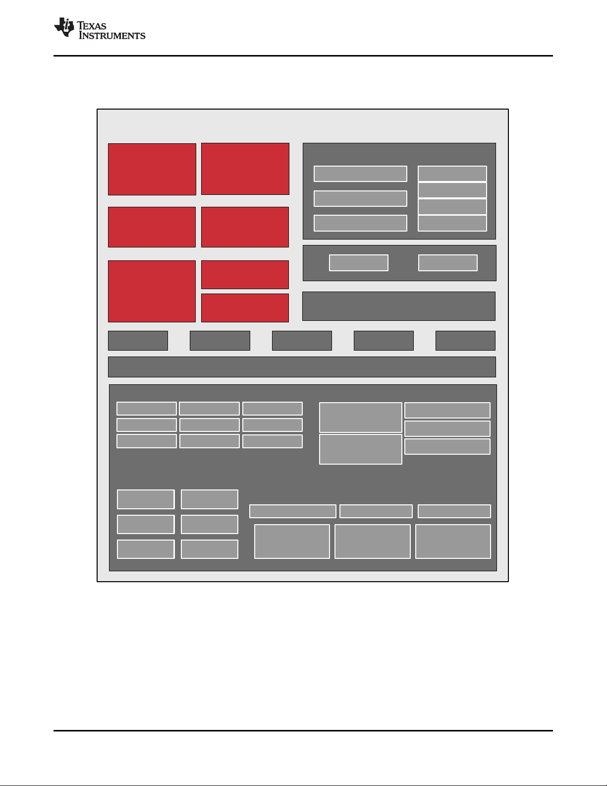
(1x C66x
Coprocessor)
Mailbox x13
EDMA
High Speed Interconnect
Program/Data Storage
Connectivity
Display Subsystem
System
(1x Arm
Cortex–A15)
IVA HD
1080p Video
Coprocessor
DSP
PCIe SS x2
(NAND/NOR/
Async)
(1x SGX544 3D)
VIP
(Dual Cortex–M4)
intro-001
GPMC / ELM
AM571x
GPU
MPU
IPU1
Serial Interfaces
I2C x5
UART x10
McSPI x4
DCAN x2
Spinlock
GPIO x8
Timers x16
WDT
QSPI
LCD1
EMIF 32-bit
DDR3(L)
SDMA
VPE
McASP x8
MMU x2
CAL
CSI2 x2
BB2D
(GC320 2D)
(Dual Cortex–M4)
IPU2
LCD2
LCD3
HDMI 1.4a
1x GFX Pipeline
3x Video Pipeline
Blend / Scale
PWM SS x3
RTC SS
HDQ
KBD
GMAC_SW
USB 3.0
Dual Role FS/HS/SS
w/ PHYs
USB 2.0
Dual Role FS/HS
w/ PHY
512-KB
OCMC_RAM
w/ ECC
SATA
DMM
MMC / SD x4
PRU-ICCS x2
Secure Boot Debug
SecurityTEE (HS devices)
www.ti.com
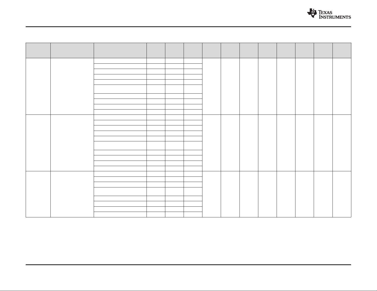
1.4 Functional Block Diagram
Figure 1-1 is functional block diagram for the device.
AM5718, AM5716
SPRS957I –MARCH 2016–REVISED NOVEMBER 2019
Figure 1-1. AM571x Block Diagram
Submit Documentation Feedback
Product Folder Links: AM5718 AM5716
Device OverviewCopyright © 2016–2019, Texas Instruments Incorporated
3

AM5718, AM5716
SPRS957I –MARCH 2016–REVISED NOVEMBER 2019
www.ti.com
Table of Contents
1 Device Overview ......................................... 1
1.1 Features .............................................. 1
1.2 Applications........................................... 2
1.3 Description............................................ 2
1.4 Functional Block Diagram ........................... 3
2 Revision History ......................................... 5
3 Device Comparison ..................................... 6
3.1 Related Products ..................................... 8
4 Terminal Configuration and Functions.............. 9
4.1 Terminal Assignment ................................. 9
4.2 Ball Characteristics.................................. 10
4.3 Multiplexing Characteristics ......................... 81
4.4 Signal Descriptions.................................. 98
5 Specifications ......................................... 141
5.1 Absolute Maximum Ratings........................ 141
5.2 ESD Ratings ....................................... 142
5.3 Power-On-Hour (POH) Limits...................... 143
5.4 Recommended Operating Conditions ............. 143
5.5 Operating Performance Points..................... 147
5.6 Power Consumption Summary .................... 165
5.7 Electrical Characteristics........................... 165
5.8 VPP Specifications for One-Time Programmable
(OTP) eFuses...................................... 175
5.9 Thermal Characteristics............................ 177
5.10 Power Supply Sequences ......................... 178
6 Clock Specifications ................................. 183
6.1 Input Clock Specifications ......................... 184
6.2 DPLLs, DLLs Specifications ....................... 193
7 Timing Requirements and Switching
Characteristics ........................................ 197
7.1 Timing Test Conditions ............................ 197
7.2 Interface Clock Specifications ..................... 197
7.3 Timing Parameters and Information ............... 197
7.4 Recommended Clock and Control Signal Transition
Behavior............................................ 199
7.5 Virtual and Manual I/O Timing Modes ............. 199
7.6 Video Input Ports (VIP) ............................ 202
7.7 Display Subsystem - Video Output Ports.......... 220
7.8 Display Subsystem - High-Definition Multimedia
Interface (HDMI) ................................... 231
7.9 Camera Serial Interface 2 CAL bridge (CSI2) ..... 232
7.10 External Memory Interface (EMIF)................. 232
7.11 General-Purpose Memory Controller (GPMC)..... 232
7.12 Timers.............................................. 256
7.13 Inter-Integrated Circuit Interface (I2C)............. 256
7.14 HDQ / 1-Wire Interface (HDQ1W) ................. 259
7.15 Universal Asynchronous Receiver Transmitter
(UART)............................................. 261
7.16 Multichannel Serial Peripheral Interface (McSPI) . 263
7.17 Quad Serial Peripheral Interface (QSPI) .......... 269
7.18 Multichannel Audio Serial Port (McASP) .......... 273
7.19 Universal Serial Bus (USB) ........................ 293
7.20 Serial Advanced Technology Attachment (SATA). 293
7.21 Peripheral Component Interconnect Express
(PCIe) .............................................. 293
7.22 Controller Area Network Interface (DCAN) ........ 294
7.23 Ethernet Interface (GMAC_SW) ................... 295
7.24 eMMC/SD/SDIO ................................... 308
7.25 General-Purpose Interface (GPIO) ................ 331
7.26 PRU-ICSS Interfaces .............................. 332
7.27 System and Miscellaneous interfaces ............. 359
7.28 Test Interfaces ..................................... 359
8 Applications, Implementation, and Layout ...... 363
8.1 Power Supply Mapping ............................ 363
8.2 DDR3 Board Design and Layout Guidelines....... 364
8.3 High Speed Differential Signal Routing Guidance. 388
8.4 Power Distribution Network Implementation
Guidance........................................... 388
8.5 Thermal Solution Guidance........................ 388
8.6 Single-Ended Interfaces ........................... 388
8.7 LJCB_REFN/P Connections....................... 390
8.8 Clock Routing Guidelines .......................... 391
9 Device and Documentation Support.............. 393
9.1 Device Nomenclature .............................. 393
9.2 Tools and Software ................................ 395
9.3 Documentation Support............................ 396
9.4 Related Links ...................................... 396
9.5 Support Resources ................................ 396
9.6 Trademarks ........................................ 396
9.7 Electrostatic Discharge Caution ................... 397
9.8 Glossary............................................ 397
10 Mechanical, Packaging, and Orderable
Information ............................................ 398
10.1 Packaging Information ............................. 398
4
Table of Contents Copyright © 2016–2019, Texas Instruments Incorporated
Submit Documentation Feedback
Product Folder Links: AM5718 AM5716
AM5718, AM5716
www.ti.com
SPRS957I –MARCH 2016–REVISED NOVEMBER 2019
2 Revision History
Changes from June 1, 2018 to April 5, 2019 (from G Revision (May 2018) to H Revision) Page
• Added Device Security Features for Silicon revision 2.1 in Section 1.1, Features........................................... 1
• Added vpp details for Silicon revision 2.1 in Table 4-1, Unused Balls Specific Connection Requirements,
Table 4-2, Ball Characteristics and Table 4-35, Power Supply Signal Descriptions ....................................... 10
• Updated OPP_HIGH power supply value in note (6) under Table 5-8, Voltage Domains Operating Performance
Points................................................................................................................................ 148
• Updated SYS_32K to FUNC_32K_CLK in Table 5-10, Maximum Supported Frequency and Section 5.10, Power
Supply Sequences ................................................................................................................ 149
• Added Section 5.8, VPP Specifications for One-Time Programmable (OTP) eFuses for Silicon revision 2.1 ........ 175
• Updated porz and rstoutn descriptions under Figure 5-2, Power-Up Sequencing........................................ 179
• Updated system clock names in Section 6, Clock Specifications ........................................................... 183
• Added PRU-ICSS sync and latch signals to IOSETs in Table 7-154, PRU-ICSS1 IOSETs and Table 7-155,
PRU-ICSS2 IOSETs............................................................................................................... 341
• Added Silicon revison 2.1 in support in Figure 9-1, Printed Device Reference and Table 9-1, Nomenclature
Description.......................................................................................................................... 393
• Updated note for cosmetic marks on package................................................................................. 393
Changes from April 6, 2019 to November 15, 2019 (from H Revision (April 2019) to I Revision) Page
• Added reminders to disable unused pulls and RX pads in Section 4.2, Ball Characteristics ............................. 11
• Removed uart2_rxd for Muxmode 0 .............................................................................................. 13
• Added clarification notes for EMU[1:0] connections in Table 4-24, GPIOs Signal Descriptions and Table 4-28,
Debug Signal Descriptions ....................................................................................................... 120
• Updated clock names in Table 5-10, Maximum Supported Frequency .................................................... 149
• Updated EMIF_DLL_FCLK max rate in Table 6-15, DLL Characteristics.................................................. 196
• Updated GPMC timing table footnotes.......................................................................................... 233
• Updated information about WD_TIMER1 in Section 7.12, Timers .......................................................... 256
• Updated parameter number in Table 7-46, Timing Requirements for QSPI............................................... 271
• Added MII_TXER timing to Section 7.23.1, GMAC MII Timings............................................................. 297
• Updated MDIO Timing Diagram and MDIO7 parameter values............................................................. 298
• Updated timing specification values for MMC.................................................................................. 312
• Updated Delay time for MMC2 in Table 7-110, Switching Characteristics for MMC2 - JC64 High Speed DDR
Mode................................................................................................................................. 320
• Added note regarding DDR ECC solutions to Table 8-4, Supported DDR3 Device Combinations..................... 365
• Added clarifications about validated DDR topology ........................................................................... 374
• Updated reference name to errata document in Section 9.3, Documentation Support .................................. 396
Submit Documentation Feedback
Product Folder Links: AM5718 AM5716
Revision HistoryCopyright © 2016–2019, Texas Instruments Incorporated
5
AM5718, AM5716
SPRS957I –MARCH 2016–REVISED NOVEMBER 2019
3 Device Comparison
Table 3-1 shows a comparison between AM571x devices, highlighting the differences. For a comparison
of the full AM57xx family of devices, refer to Parametric Table.
www.ti.com
Table 3-1. Device Comparison
FEATURES
AM5718 AM5716
DEVICE
Features
CTRL_WKUP_STD_FUSE_DIE_ID_2[31:24] Base PN register bit field value
(3)
AM5718: 55 (0x37) AM5716: 53 (0x35)
AM5718-E: 56 (0x38) AM5716-E: 54 (0x36)
Processors/ Accelerators
Speed Grades X X, D
Arm Single Cortex-A15 Microprocessor Subsystem
MPU core 0 Yes
(MPU)
C66x VLIW DSP DSP1 Yes
BitBLT 2D Hardware Acceleration Engine (BB2D) BB2D Yes Not Supported
Display Subsystem VOUT1 Yes Not Supported
VOUT2 Yes Not Supported
VOUT3 Yes Not Supported
HDMI Yes Not Supported
Dual Arm Cortex-M4 Image Processing Unit (IPU) IPU1 Yes
IPU2 Yes
Image Video Accelarator (IVA) IVA Yes Not Supported
SGX544 Single-Core 3D Graphics Processing Unit
GPU Yes Not Supported
(GPU)
Video Input Port 1 (VIP1) vin1a Yes
vin1b Yes
vin2a Yes
vin2b Yes
Video Processing Engine (VPE) VPE Yes
Program/Data Storage
On-Chip Shared Memory (RAM) OCMC_RAM1 512KB
General-Purpose Memory Controller (GPMC) GPMC Yes
DDR3 Memory Controller EMIF1 up to 2GB across single chip select
Dynamic Memory Manager (DMM) DMM Yes
Radio Support
Audio Tracking Logic (ATL) ATL Not Supported
Viterbi Coprocessor (VCP) VCP1 Not Supported
VCP2 Not Supported
(1)
(1)
(1)
Peripherals
Dual Controller Area Network (DCAN) Interface DCAN1 Yes
DCAN2 Yes
Enhanced DMA (EDMA) EDMA Yes
System DMA (DMA_SYSTEM) DMA_SYSTEM Yes
Ethernet Subsystem (Ethernet SS) GMAC_SW[0] MII, RMII, or RGMII
GMAC_SW[1] MII, RMII, or RGMII
General Purpose I/O (GPIO) GPIO up to 215
Inter-Integrated Circuit (I2C) Interface I2C 5
System Mailbox Module MAILBOX 13 13
(1)
(1)
(1)
(1)
(1)
(1)
(1)
6
Device Comparison Copyright © 2016–2019, Texas Instruments Incorporated
Submit Documentation Feedback
Product Folder Links: AM5718 AM5716
AM5718, AM5716
www.ti.com
SPRS957I –MARCH 2016–REVISED NOVEMBER 2019
Table 3-1. Device Comparison (continued)
FEATURES
AM5718 AM5716
Media Local Bus Subsystem MLB Not Supported
Camera Adaptation Layer (CAL) Camera Serial
Interface 2 (CSI2)
CSI2_0 Yes
CSI2_1 Yes
Multichannel Audio Serial Port (McASP) McASP1 16 serializers
McASP2 16 serializers
McASP3 4 serializers
McASP4 4 serializers
McASP5 4 serializers
McASP6 4 serializers
McASP7 4 serializers
McASP8 4 serializers
MultiMedia Card/Secure Digital/Secure Digital Input
Output Interface (MMC/SD/SDIO)
MMC1 1x UHSI 4b
MMC2 1x eMMC™ 8b
MMC3 1x SDIO 8b
MMC4 1x SDIO 4b
PCI-Express 3.0 Port with Integrated PHY PCIe_SS1 up to two lanes (second lane shared with
PCIe_SS2 Single lane (shared with PCIe_SS1 and USB1)
2x Programmable Real-Time Unit Subsystem and
Industrial Communication Subsystem (PRU-ICSS)
PRU-ICSS1 Yes
PRU-ICSS2 Yes
Serial Advanced Technology Attachment (SATA) SATA Yes
Real-Time Clock Subsystem (RTCSS)
(2)
RTCSS Yes
Multichannel Serial Peripheral Interface (McSPI) McSPI 4
HDQ1W HDQ1W Yes
Quad SPI (QSPI) QSPI Yes
Spinlock Module SPINLOCK Yes
Keyboard Controller (KBD) KBD Yes
Timers, General-Purpose TIMERS GP 16
Timer, Watchdog WD TIMER Yes
Pulse-Width Modulation Subsystem (PWMSS) PWMSS1 Yes
PWMSS2 Yes
PWMSS3 Yes
Universal Asynchronous Receiver/Transmitter
UART 10
(UART)
Universal Serial Bus (USB3.0) USB1 (SuperSpeed, Dual-Role-
Device [DRD]
Universal Serial Bus (USB2.0) USB2 (High Speed, Dual-Role-
Device [DRD], with embedded HS
PHY)
USB3 (High Speed, OTG2.0, with
ULPI)
USB4 (High Speed, OTG2.0, with
ULPI)
(1) Features noted as “not supported,” must not be used. Their functionality is not supported by TI for this family of devices. These features
are subject to removal without notice on future device revisions. Any information regarding the unsupported features has been retained
in the documentation solely for the purpose of clarifying signal names or for consistency with previous feature descriptions.
(2) RTC-only mode is not a supported feature.
(3) For more details about the CTRL_WKUP_STD_FUSE_DIE_ID_2 register and Base PN bit field, see the AM571x Technical Reference
Manual.
DEVICE
(1)
PCIe_SS2 and USB1)
Yes
Yes
Not Supported
Not Supported
(1)
(1)
Submit Documentation Feedback
Product Folder Links: AM5718 AM5716
Device ComparisonCopyright © 2016–2019, Texas Instruments Incorporated
7

AM5718, AM5716
SPRS957I –MARCH 2016–REVISED NOVEMBER 2019
3.1 Related Products
Sitara™ processors Broad family of scalable processors based on Arm® Cortex®-A cores and TI C66x
DSP cores with flexible accelerators, peripherals, connectivity and unified software support –
perfect for sensors to servers. Sitara processors have the reliability needed for use in
industrial applications.
AM57x Sitara™ processors AM57x Sitara™ processors are highly integrated devices that enable high-
performance and multimedia applications. In addition to the Arm® Cortex®-A15 cores and TI
C66x DSP cores, on-board accelerators provide enhanced vision and machine learning
capabilities, support for multiple industrial Ethernet protocols, and video processing.
Sitara™ processors applications Sitara™ processors provide scalable solutions for a wide range of
applications from HMIs and gateways to more complex equipment such as drives and
substation automation equipment. Sitara processors also offer multi-protocol support for
industrial communication protocols such as EtherCAT®, Ethernet/IP, and Profinet.
Reference Designs and Evaluation Modules TI provides many reference designs containing ‘building
block’ solutions to enable customers to rapidly develop their own unique products and
solutions. EVMs are also provided to help kick-start product development.
Companion Products for AM571x Review products that are frequently purchased or used in conjunction
with this product to complete your design.
www.ti.com
8
Device Comparison Copyright © 2016–2019, Texas Instruments Incorporated
Submit Documentation Feedback
Product Folder Links: AM5718 AM5716
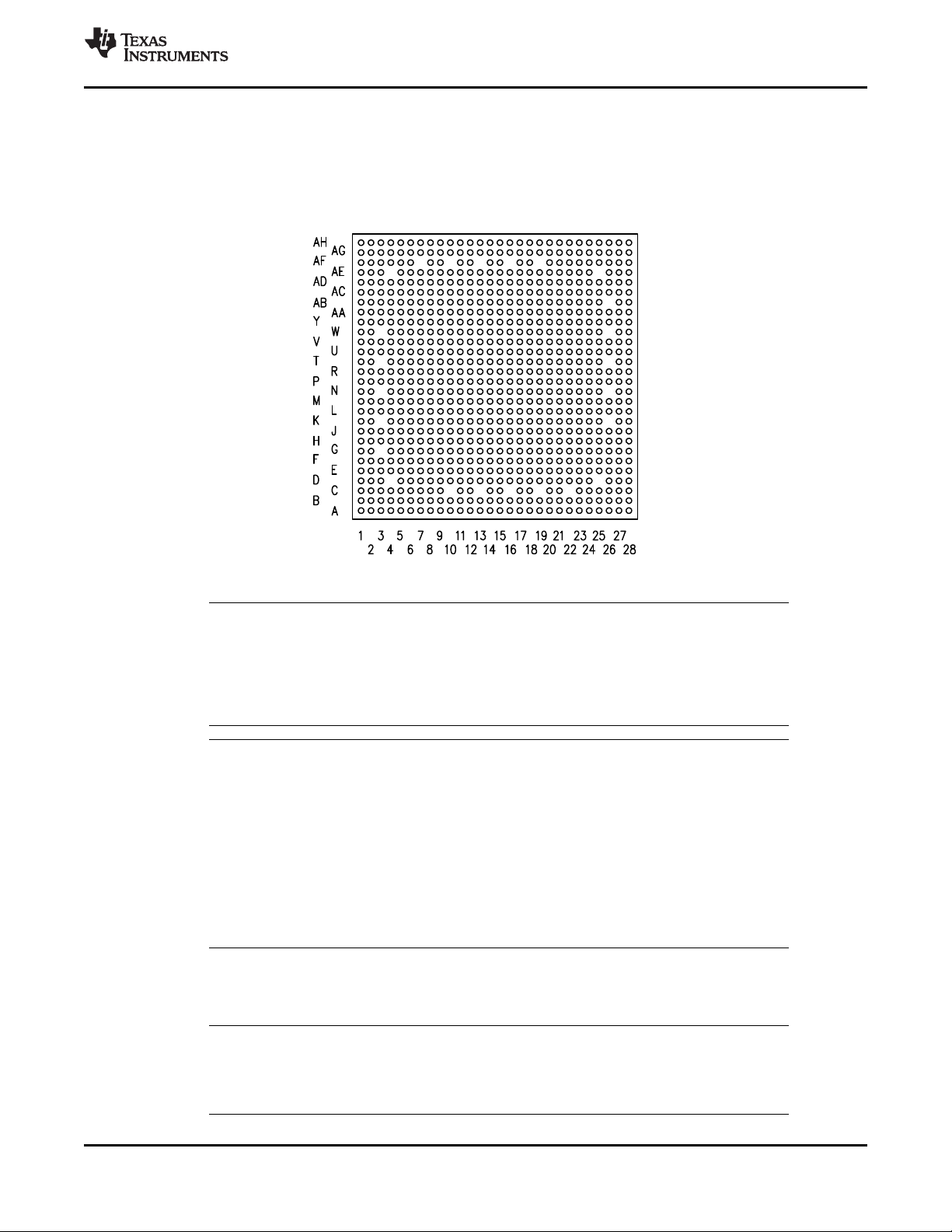
SPRS906_BALL_01
www.ti.com
4 Terminal Configuration and Functions
4.1 Terminal Assignment
Figure 4-1 shows the ball locations for the 760 plastic ball grid array (PBGA) package and is used in
conjunction with Table 4-2 through Table 4-35 to locate signal names and ball grid numbers.
AM5718, AM5716
SPRS957I –MARCH 2016–REVISED NOVEMBER 2019
Figure 4-1. ABC S-PBGA-N760 Package (Bottom View)
The following bottom balls are not pinned out: AF7 / AF10 / AF13 / AF16 / AF19 / AE4 /
AE25 / AB26 / W3 / W26 / T3 / T26 / N3 / N26 / K3 / K26 / G3 / D4 / D25 / C10 / C13 / C16 /
C19 / C22.
These balls do not exist on the package.
The following bottom balls are not connected: AH11 / AH12 / AG2 / AG8 / AG11 / AG12 /
AF4 / AF6 / AF8 / AF9 / AE3 / AE5 / AE6 / AE8 / AE9 / AD3 / AD8 / AD9 / Y15 / Y16 / V18 /
V19 / U18 / U19 / U22 / U23 / U24 / U25 / U26 / U27 / U28 / T22 / T23 / T27 / T28 / R20 /
R22 / R23 / R24 / R25 / R26 / R27 / R28 / P19 / P22 / P23 / P24 / P25 / P26 / P27 / N20 /
N22 / N23 / N27 / N28 / M20 / M21 / M22 / M23 / M24 / M25 / M26 / M27 / M28 / L20 / L21 /
L22 / L23 / L24 / L25 / L26 / L27 / L28 / K20 / K21 / K22 / K23 / K27 / K28 / J20 / J21 / J22 /
J23 / J24 / J25 / J26 / J27 / H20 / H21 / H22 / H23 / H24 / H25 / H26 / H27 / H28 / G22 /
G23 / G24 / G25 / G26 / G27 / G28 / F24 / F25 / F26 / F27 / F28 / E24 / E26 / E27 / E28.
These balls can be connected as desired, including to vss.
4.1.1 Unused Balls Connection Requirements
This section describes the Unused/Reserved balls connection requirements.
NOTE
NOTE
NOTE
The following balls are reserved: A27 / Y5 / Y10 / B28
These balls must be left unconnected.
Submit Documentation Feedback
Product Folder Links: AM5718 AM5716
Terminal Configuration and FunctionsCopyright © 2016–2019, Texas Instruments Incorporated
9
AM5718, AM5716
SPRS957I –MARCH 2016–REVISED NOVEMBER 2019
All unused power supply balls must be supplied with the voltages specified in the
Section 5.4, Recommended Operating Conditions, unless alternative tie-off options are
included in Section 4.4, Signal Descriptions.
Table 4-1. Unused Balls Specific Connection Requirements
BALLS CONNECTION REQUIREMENTS
AE15 / AC15 / AE14 / D20 / AD17 / AC16 / V27 / AH25 / AE27 /
AD27 / Y28
E20 / D21 / E23 / C20 / C21 / V28 / F18 / AG25 / AE28 / AD28 / Y27
/ F17 / C25
K14 (vpp) This ball must be left unconnected if unused
AF14 (rtc_iso)
AB17 (rtc_porz)
www.ti.com
NOTE
These balls must be connected to GND through an external pull
resistor if unused
These balls must be connected to the corresponding power supply
through an external pull resistor if unused
This ball should be connected to the corresponding power supply
through an external pull resistor if unused; or can be connected to
F22 (porz) when RTC unused (level translation may be needed)
This ball should be connected to VSS when RTC is unused; or can
be connected to F22 (porz) when RTC unused (level translation may
be needed)
All other unused signal balls with a Pad Configuration Register can be left unconnected with
their internal pullup or pulldown resistor enabled.
All other unused signal balls without a Pad Configuration Register can be left unconnected.
4.2 Ball Characteristics
Table 4-2 describes the terminal characteristics and the signals multiplexed on each ball. The following list
describes the table column headers:
1. BALL NUMBER: Ball number(s) on the bottom side associated with each signal on the bottom.
2. BALL NAME: Mechanical name from package device (name is taken from muxmode 0).
3. SIGNAL NAME: Names of signals multiplexed on each ball (also notice that the name of the ball is the
signal name in muxmode 0).
Table 4-2 does not take into account the subsystem multiplexing signals. Subsystem
multiplexing signals are described in Section 4.4, Signal Descriptions.
In the Driver off mode, the buffer is configured in high-impedance.
NOTE
NOTE
NOTE
NOTE
10
Terminal Configuration and Functions Copyright © 2016–2019, Texas Instruments Incorporated
Submit Documentation Feedback
Product Folder Links: AM5718 AM5716

www.ti.com
4. PN: This column shows if the functionality is applicable for AM5716 device. Note that the Ball
5. MUXMODE: Multiplexing mode number:
AM5718, AM5716
SPRS957I –MARCH 2016–REVISED NOVEMBER 2019
NOTE
In some cases Table 4-2 may present more than one signal name per muxmode for the
same ball. First signal in the list is the dominant function as selected via
CTRL_CORE_PAD_* register.
All other signals are virtual functions that present alternate multiplexing options. This virtual
functions are controlled via CTRL_CORE_ALT_SELECT_MUX or
CTRL_CORE_VIP_MUX_SELECT register. For more information on how to use these
options, see Pad Configuration Registers section, Control Module chapter in the device TRM.
Characteristics table presents a functionality of AM5718. If the cell is empty it means that the signal is
available in all devices.
- Yes - Functionality is presented in AM5716
- No - Functionality is not presented in AM5716
An empty box means Yes.
a. MUXMODE 0 is the primary mode; this means that when MUXMODE=0 is set, the function
mapped on the pin corresponds to the name of the pin. The primary muxmode is not necessarily
the default muxmode.
NOTE
The default mode is the mode at the release of the reset; also see the RESET REL.
MUXMODE column.
b. MUXMODE 1 through 15 are possible muxmodes for alternate functions. On each pin, some
muxmodes are effectively used for alternate functions, while some muxmodes are not used. Only
MUXMODE values which correspond to defined functions should be used.
c. An empty box means Not Applicable.
6. TYPE: Signal type and direction:
– I = Input
– O = Output
– IO = Input or Output
– D = Open drain
– DS = Differential Signaling
– A = Analog
– PWR = Power
– GND = Ground
– CAP = LDO Capacitor
NOTE
The RX buffer within the pad logic should be disabled on all pins that are not being used as
an input. For more information, see the Control Module / Control Module Functional
Description / PAD Functional Multiplexing and Configuration section in the device TRM.
7. BALL RESET STATE: The state of the terminal at power-on reset:
– drive 0 (OFF): The buffer drives VOL(pulldown or pullup resistor not activated).
– drive 1 (OFF): The buffer drives VOH(pulldown or pullup resistor not activated).
– OFF: High-impedance
– PD: High-impedance with an active pulldown resistor
– PU: High-impedance with an active pullup resistor
– An empty box means Not Applicable
Terminal Configuration and FunctionsCopyright © 2016–2019, Texas Instruments Incorporated
Submit Documentation Feedback
Product Folder Links: AM5718 AM5716
11

AM5718, AM5716
SPRS957I –MARCH 2016–REVISED NOVEMBER 2019
Designs that contain pullup or pulldown resistors, either on the board or in attached devices
that oppose internal pullup or pulldown resistors, that are active while the device is held in
reset, must not remain in reset for long periods of time.
8. BALL RESET REL. STATE: The state of the terminal at the deactivation of the rstoutn signal (also
mapped to the PRCM SYS_WARM_OUT_RST signal).
– drive 0 (OFF): The buffer drives VOL(pulldown or pullup resistor not activated).
– drive clk (OFF): The buffer drives a toggling clock (pulldown or pullup resistor not activated).
– drive 1 (OFF): The buffer drives VOH(pulldown or pullup resistor not activated).
– OFF: High-impedance
– PD: High-impedance with an active pulldown resistor
– PU: High-impedance with an active pullup resistor
– An empty box means Not Applicable
For more information on the CORE_PWRON_RET_RST reset signal and its reset sources,
see Power, Reset, and Clock Management chapter in the device TRM.
9. BALL RESET REL. MUXMODE: This muxmode is automatically configured at the release of the
rstoutn signal (also mapped to the PRCM SYS_WARM_OUT_RST signal).
An empty box means Not Applicable.
10. IO VOLTAGE VALUE: This column describes the IO voltage value (VDDS supply).
An empty box means Not Applicable.
11. POWER: The voltage supply that powers the terminal IO buffers.
An empty box means Not Applicable.
www.ti.com
NOTE
NOTE
NOTE
VOUT1, VOUT2 and VOUT3 are only supported at 1.8V and not at 3.3V. This must be
considered in the pin mux programming and VDDSHVx supply connections.
12. HYS: Indicates if the input buffer is with hysteresis:
– Yes: With hysteresis
– No: Without hysteresis
– An empty box: Not Applicable
NOTE
For more information, see the hysteresis values in Section 5.7, Electrical Characteristics.
13. BUFFER TYPE: Drive strength of the associated output buffer.
An empty box means Not Applicable.
NOTE
For programmable buffer strength:
– The default value is given in Table 4-2.
– A note describes all possible values according to the selected muxmode.
14. PULLUP / PULLDOWN TYPE: Denotes the presence of an internal pullup or pulldown resistor.
Pullup and pulldown resistors can be enabled or disabled via software.
– PU: Internal pullup
– PD: Internal pulldown
– PU/PD: Internal pullup and pulldown
12
Terminal Configuration and Functions Copyright © 2016–2019, Texas Instruments Incorporated
Submit Documentation Feedback
Product Folder Links: AM5718 AM5716

www.ti.com
15. DSIS: The deselected input state (DSIS) indicates the state driven on the peripheral input (logic "0" or
AM5718, AM5716
SPRS957I –MARCH 2016–REVISED NOVEMBER 2019
– PUx/PDy: Programmable internal pullup and pulldown
– PDy: Programmable internal pulldown
– An empty box means No pull
NOTE
Internal pullup or pulldown resistors must be disabled when opposed by an external pullup or
pulldown resistor on the board or within an attached device.
logic "1") when the peripheral pin function is not selected by any of the PINCNTLx registers.
– 0: Logic 0 driven on the peripheral's input signal port.
– 1: Logic 1 driven on the peripheral's input signal port.
– blank: Pin state driven on the peripheral's input signal port.
NOTE
Configuring two pins to the same input signal is not supported as it can yield unexpected
results. This can be easily prevented with the proper software configuration (Hi-Z mode is not
an input signal).
NOTE
When a pad is set into a multiplexing mode which is not defined by pin multiplexing, that
pad’s behavior is undefined. This should be avoided.
NOTE
Some of the EMIF1 signals have an additional state change at the release of porz. The state
that the signals change to at the release of porz is as follows:
drive 0 (OFF) for: ddr1_csn0, ddr1_ck, ddr1_nck, ddr1_casn, ddr1_rasn, ddr1_wen,
ddr1_ba[2:0], ddr1_a[15:0].
OFF for: ddr1_ecc_d[7:0], ddr1_dqm[3:0], ddr1_dqm_ecc, ddr1_dqs[3:0], ddr1_dqsn[3:0],
ddr1_dqs_ecc, ddr1_dqsn_ecc, ddr1_d[31:0].
NOTE
Dual rank support is not available on this device, but signal names are retained for
consistency with the AM57xx family of devices.
Submit Documentation Feedback
Product Folder Links: AM5718 AM5716
Terminal Configuration and FunctionsCopyright © 2016–2019, Texas Instruments Incorporated
13
AM5718, AM5716
SPRS957I –MARCH 2016–REVISED NOVEMBER 2019
www.ti.com
BALL
RESET
(1)
BALL
RESET REL.
STATE [8]
BALL
RESET REL.
MUXMODE
[9]
I/O
VOLTAGE
VALUE [10]
POWER [11] HYS [12]
BUFFER
TYPE [13]
CSI2
CSI2
CSI2
CSI2
CSI2
CSI2
CSI2
CSI2
CSI2
CSI2
CSI2
CSI2
CSI2
CSI2
CSI2
CSI2
Table 4-2. Ball Characteristics
BALL NUMBER
[1]
K9 cap_vbbldo_dsp cap_vbbldo_dsp CAP
Y14 cap_vbbldo_gpu cap_vbbldo_gpu CAP
J10 cap_vbbldo_iva cap_vbbldo_iva CAP
J16 cap_vbbldo_mpu cap_vbbldo_mpu CAP
T20 cap_vddram_core1 cap_vddram_core1 CAP
L9 cap_vddram_core3 cap_vddram_core3 CAP
J19 cap_vddram_core4 cap_vddram_core4 CAP
J9 cap_vddram_dsp cap_vddram_dsp CAP
Y13 cap_vddram_gpu cap_vddram_gpu CAP
K16 cap_vddram_iva cap_vddram_iva CAP
K19 cap_vddram_mpu cap_vddram_mpu CAP
AE1 csi2_0_dx0 csi2_0_dx0 0 I 1.8 vdda_csi Yes LVCMOS
AF1 csi2_0_dx1 csi2_0_dx1 0 I 1.8 vdda_csi Yes LVCMOS
AF2 csi2_0_dx2 csi2_0_dx2 0 I 1.8 vdda_csi Yes LVCMOS
AH4 csi2_0_dx3 csi2_0_dx3 0 I 1.8 vdda_csi Yes LVCMOS
AH3 csi2_0_dx4 csi2_0_dx4 0 I 1.8 vdda_csi Yes LVCMOS
AD2 csi2_0_dy0 csi2_0_dy0 0 I 1.8 vdda_csi Yes LVCMOS
AE2 csi2_0_dy1 csi2_0_dy1 0 I 1.8 vdda_csi Yes LVCMOS
AF3 csi2_0_dy2 csi2_0_dy2 0 I 1.8 vdda_csi Yes LVCMOS
AG4 csi2_0_dy3 csi2_0_dy3 0 I 1.8 vdda_csi Yes LVCMOS
AG3 csi2_0_dy4 csi2_0_dy4 0 I 1.8 vdda_csi Yes LVCMOS
AG5 csi2_1_dx0 csi2_1_dx0 0 I 1.8 vdda_csi Yes LVCMOS
AG6 csi2_1_dx1 csi2_1_dx1 0 I 1.8 vdda_csi Yes LVCMOS
AH7 csi2_1_dx2 csi2_1_dx2 0 I 1.8 vdda_csi Yes LVCMOS
AH5 csi2_1_dy0 csi2_1_dy0 0 I 1.8 vdda_csi Yes LVCMOS
AH6 csi2_1_dy1 csi2_1_dy1 0 I 1.8 vdda_csi Yes LVCMOS
AG7 csi2_1_dy2 csi2_1_dy2 0 I 1.8 vdda_csi Yes LVCMOS
BALL NAME [2] SIGNAL NAME [3] PN [4]
MUXMODE
[5]
TYPE [6]
STATE [7]
PULL
UP/DOWN
TYPE [14]
PU/PD
PU/PD
PU/PD
PU/PD
PU/PD
PU/PD
PU/PD
PU/PD
PU/PD
PU/PD
PU/PD
PU/PD
PU/PD
PU/PD
PU/PD
PU/PD
14
Copyright © 2016–2019, Texas Instruments IncorporatedTerminal Configuration and Functions
Submit Documentation Feedback
Product Folder Links: AM5718 AM5716
www.ti.com
AM5718, AM5716
SPRS957I –MARCH 2016–REVISED NOVEMBER 2019
Table 4-2. Ball Characteristics
BALL NUMBER
[1]
G19 dcan1_rx dcan1_rx 0 IO PU PU 15 1.8/3.3 vddshv3 Yes Dual Voltage
G20 dcan1_tx dcan1_tx 0 IO PU PU 15 1.8/3.3 vddshv3 Yes Dual Voltage
AD20 ddr1_a0 ddr1_a0 0 O PD drive 1 (OFF) 1.35/1.5 vdds_ddr1 No LVCMOS
AC19 ddr1_a1 ddr1_a1 0 O PD drive 1 (OFF) 1.35/1.5 vdds_ddr1 No LVCMOS
AC20 ddr1_a2 ddr1_a2 0 O PD drive 1 (OFF) 1.35/1.5 vdds_ddr1 No LVCMOS
AB19 ddr1_a3 ddr1_a3 0 O PD drive 1 (OFF) 1.35/1.5 vdds_ddr1 No LVCMOS
AF21 ddr1_a4 ddr1_a4 0 O PD drive 1 (OFF) 1.35/1.5 vdds_ddr1 No LVCMOS
AH22 ddr1_a5 ddr1_a5 0 O PD drive 1 (OFF) 1.35/1.5 vdds_ddr1 No LVCMOS
AG23 ddr1_a6 ddr1_a6 0 O PD drive 1 (OFF) 1.35/1.5 vdds_ddr1 No LVCMOS
AE21 ddr1_a7 ddr1_a7 0 O PD drive 1 (OFF) 1.35/1.5 vdds_ddr1 No LVCMOS
AF22 ddr1_a8 ddr1_a8 0 O PD drive 1 (OFF) 1.35/1.5 vdds_ddr1 No LVCMOS
AE22 ddr1_a9 ddr1_a9 0 O PD drive 1 (OFF) 1.35/1.5 vdds_ddr1 No LVCMOS
AD21 ddr1_a10 ddr1_a10 0 O PD drive 1 (OFF) 1.35/1.5 vdds_ddr1 No LVCMOS
AD22 ddr1_a11 ddr1_a11 0 O PD drive 1 (OFF) 1.35/1.5 vdds_ddr1 No LVCMOS
AC21 ddr1_a12 ddr1_a12 0 O PD drive 1 (OFF) 1.35/1.5 vdds_ddr1 No LVCMOS
AF18 ddr1_a13 ddr1_a13 0 O PD drive 1 (OFF) 1.35/1.5 vdds_ddr1 No LVCMOS
AE17 ddr1_a14 ddr1_a14 0 O PD drive 1 (OFF) 1.35/1.5 vdds_ddr1 No LVCMOS
BALL NAME [2] SIGNAL NAME [3] PN [4]
uart8_txd 2 O
mmc2_sdwp 3 I
sata1_led 4 O
hdmi1_cec No 6 IO
gpio1_15 14 IO
Driver off 15 I
uart8_rxd 2 I
mmc2_sdcd 3 I
hdmi1_hpd No 6 IO
gpio1_14 14 IO
Driver off 15 I
MUXMODE
[5]
TYPE [6]
(1)
(continued)
BALL
RESET
STATE [7]
BALL
RESET REL.
STATE [8]
BALL
RESET REL.
MUXMODE
[9]
I/O
VOLTAGE
VALUE [10]
POWER [11] HYS [12]
BUFFER
TYPE [13]
LVCMOS
LVCMOS
DDR
DDR
DDR
DDR
DDR
DDR
DDR
DDR
DDR
DDR
DDR
DDR
DDR
DDR
DDR
PULL
UP/DOWN
TYPE [14]
PU/PD
PU/PD
PUx/PDy
PUx/PDy
PUx/PDy
PUx/PDy
PUx/PDy
PUx/PDy
PUx/PDy
PUx/PDy
PUx/PDy
PUx/PDy
PUx/PDy
PUx/PDy
PUx/PDy
PUx/PDy
PUx/PDy
Copyright © 2016–2019, Texas Instruments Incorporated Terminal Configuration and Functions
Submit Documentation Feedback
Product Folder Links: AM5718 AM5716
15

AM5718, AM5716
SPRS957I –MARCH 2016–REVISED NOVEMBER 2019
www.ti.com
Table 4-2. Ball Characteristics
BALL NUMBER
[1]
AD18 ddr1_a15 ddr1_a15 0 O PD drive 1 (OFF) 1.35/1.5 vdds_ddr1 No LVCMOS
AF17 ddr1_ba0 ddr1_ba0 0 O PU drive 1 (OFF) 1.35/1.5 vdds_ddr1 No LVCMOS
AE18 ddr1_ba1 ddr1_ba1 0 O PU drive 1 (OFF) 1.35/1.5 vdds_ddr1 No LVCMOS
AB18 ddr1_ba2 ddr1_ba2 0 O PU drive 1 (OFF) 1.35/1.5 vdds_ddr1 No LVCMOS
AC18 ddr1_casn ddr1_casn 0 O PU drive 1 (OFF) 1.35/1.5 vdds_ddr1 No LVCMOS
AG24 ddr1_ck ddr1_ck 0 O PD drive 0 (OFF) 1.35/1.5 vdds_ddr1 No LVCMOS
AG22 ddr1_cke ddr1_cke 0 O PU drive 1 (OFF) 1.35/1.5 vdds_ddr1 No LVCMOS
AH23 ddr1_csn0 ddr1_csn0 0 O PU drive 1 (OFF) 1.35/1.5 vdds_ddr1 No LVCMOS
AB16 ddr1_csn1 ddr1_csn1 0 O PU drive 1 (OFF) 1.35/1.5 vdds_ddr1 No LVCMOS
AF25 ddr1_d0 ddr1_d0 0 IO PD PD 1.35/1.5 vdds_ddr1 No LVCMOS
AF26 ddr1_d1 ddr1_d1 0 IO PD PD 1.35/1.5 vdds_ddr1 No LVCMOS
AG26 ddr1_d2 ddr1_d2 0 IO PD PD 1.35/1.5 vdds_ddr1 No LVCMOS
AH26 ddr1_d3 ddr1_d3 0 IO PD PD 1.35/1.5 vdds_ddr1 No LVCMOS
AF24 ddr1_d4 ddr1_d4 0 IO PD PD 1.35/1.5 vdds_ddr1 No LVCMOS
AE24 ddr1_d5 ddr1_d5 0 IO PD PD 1.35/1.5 vdds_ddr1 No LVCMOS
AF23 ddr1_d6 ddr1_d6 0 IO PD PD 1.35/1.5 vdds_ddr1 No LVCMOS
AE23 ddr1_d7 ddr1_d7 0 IO PD PD 1.35/1.5 vdds_ddr1 No LVCMOS
AC23 ddr1_d8 ddr1_d8 0 IO PD PD 1.35/1.5 vdds_ddr1 No LVCMOS
AF27 ddr1_d9 ddr1_d9 0 IO PD PD 1.35/1.5 vdds_ddr1 No LVCMOS
AG27 ddr1_d10 ddr1_d10 0 IO PD PD 1.35/1.5 vdds_ddr1 No LVCMOS
AF28 ddr1_d11 ddr1_d11 0 IO PD PD 1.35/1.5 vdds_ddr1 No LVCMOS
AE26 ddr1_d12 ddr1_d12 0 IO PD PD 1.35/1.5 vdds_ddr1 No LVCMOS
AC25 ddr1_d13 ddr1_d13 0 IO PD PD 1.35/1.5 vdds_ddr1 No LVCMOS
BALL NAME [2] SIGNAL NAME [3] PN [4]
MUXMODE
[5]
TYPE [6]
(1)
(continued)
BALL
RESET
STATE [7]
BALL
RESET REL.
STATE [8]
BALL
RESET REL.
MUXMODE
[9]
I/O
VOLTAGE
VALUE [10]
POWER [11] HYS [12]
BUFFER
TYPE [13]
DDR
DDR
DDR
DDR
DDR
DDR
DDR
DDR
DDR
DDR
DDR
DDR
DDR
DDR
DDR
DDR
DDR
DDR
DDR
DDR
DDR
DDR
DDR
PULL
UP/DOWN
TYPE [14]
PUx/PDy
PUx/PDy
PUx/PDy
PUx/PDy
PUx/PDy
PUx/PDy
PUx/PDy
PUx/PDy
PUx/PDy
PUx/PDy
PUx/PDy
PUx/PDy
PUx/PDy
PUx/PDy
PUx/PDy
PUx/PDy
PUx/PDy
PUx/PDy
PUx/PDy
PUx/PDy
PUx/PDy
PUx/PDy
PUx/PDy
16
Copyright © 2016–2019, Texas Instruments IncorporatedTerminal Configuration and Functions
Submit Documentation Feedback
Product Folder Links: AM5718 AM5716
www.ti.com
AM5718, AM5716
SPRS957I –MARCH 2016–REVISED NOVEMBER 2019
Table 4-2. Ball Characteristics
BALL NUMBER
[1]
AC24 ddr1_d14 ddr1_d14 0 IO PD PD 1.35/1.5 vdds_ddr1 No LVCMOS
AD25 ddr1_d15 ddr1_d15 0 IO PD PD 1.35/1.5 vdds_ddr1 No LVCMOS
V20 ddr1_d16 ddr1_d16 0 IO PD PD 1.35/1.5 vdds_ddr1 No LVCMOS
W20 ddr1_d17 ddr1_d17 0 IO PD PD 1.35/1.5 vdds_ddr1 No LVCMOS
AB28 ddr1_d18 ddr1_d18 0 IO PD PD 1.35/1.5 vdds_ddr1 No LVCMOS
AC28 ddr1_d19 ddr1_d19 0 IO PD PD 1.35/1.5 vdds_ddr1 No LVCMOS
AC27 ddr1_d20 ddr1_d20 0 IO PD PD 1.35/1.5 vdds_ddr1 No LVCMOS
Y19 ddr1_d21 ddr1_d21 0 IO PD PD 1.35/1.5 vdds_ddr1 No LVCMOS
AB27 ddr1_d22 ddr1_d22 0 IO PD PD 1.35/1.5 vdds_ddr1 No LVCMOS
Y20 ddr1_d23 ddr1_d23 0 IO PD PD 1.35/1.5 vdds_ddr1 No LVCMOS
AA23 ddr1_d24 ddr1_d24 0 IO PD PD 1.35/1.5 vdds_ddr1 No LVCMOS
Y22 ddr1_d25 ddr1_d25 0 IO PD PD 1.35/1.5 vdds_ddr1 No LVCMOS
Y23 ddr1_d26 ddr1_d26 0 IO PD PD 1.35/1.5 vdds_ddr1 No LVCMOS
AA24 ddr1_d27 ddr1_d27 0 IO PD PD 1.35/1.5 vdds_ddr1 No LVCMOS
Y24 ddr1_d28 ddr1_d28 0 IO PD PD 1.35/1.5 vdds_ddr1 No LVCMOS
AA26 ddr1_d29 ddr1_d29 0 IO PD PD 1.35/1.5 vdds_ddr1 No LVCMOS
AA25 ddr1_d30 ddr1_d30 0 IO PD PD 1.35/1.5 vdds_ddr1 No LVCMOS
AA28 ddr1_d31 ddr1_d31 0 IO PD PD 1.35/1.5 vdds_ddr1 No LVCMOS
AD23 ddr1_dqm0 ddr1_dqm0 0 O PU drive 1 (OFF) 1.35/1.5 vdds_ddr1 No LVCMOS
AB23 ddr1_dqm1 ddr1_dqm1 0 O PU drive 1 (OFF) 1.35/1.5 vdds_ddr1 No LVCMOS
AC26 ddr1_dqm2 ddr1_dqm2 0 O PU drive 1 (OFF) 1.35/1.5 vdds_ddr1 No LVCMOS
AA27 ddr1_dqm3 ddr1_dqm3 0 O PU drive 1 (OFF) 1.35/1.5 vdds_ddr1 No LVCMOS
V26 ddr1_dqm_ecc ddr1_dqm_ecc 0 O PU drive 1 (OFF) 1.35/1.5 vdds_ddr1 No LVCMOS
BALL NAME [2] SIGNAL NAME [3] PN [4]
MUXMODE
[5]
TYPE [6]
(1)
(continued)
BALL
RESET
STATE [7]
BALL
RESET REL.
STATE [8]
BALL
RESET REL.
MUXMODE
[9]
I/O
VOLTAGE
VALUE [10]
POWER [11] HYS [12]
BUFFER
TYPE [13]
DDR
DDR
DDR
DDR
DDR
DDR
DDR
DDR
DDR
DDR
DDR
DDR
DDR
DDR
DDR
DDR
DDR
DDR
DDR
DDR
DDR
DDR
DDR
PULL
UP/DOWN
TYPE [14]
PUx/PDy
PUx/PDy
PUx/PDy
PUx/PDy
PUx/PDy
PUx/PDy
PUx/PDy
PUx/PDy
PUx/PDy
PUx/PDy
PUx/PDy
PUx/PDy
PUx/PDy
PUx/PDy
PUx/PDy
PUx/PDy
PUx/PDy
PUx/PDy
PUx/PDy
PUx/PDy
PUx/PDy
PUx/PDy
PUx/PDy
Copyright © 2016–2019, Texas Instruments Incorporated Terminal Configuration and Functions
Submit Documentation Feedback
Product Folder Links: AM5718 AM5716
17

AM5718, AM5716
SPRS957I –MARCH 2016–REVISED NOVEMBER 2019
www.ti.com
Table 4-2. Ball Characteristics
BALL NUMBER
[1]
AH25 ddr1_dqs0 ddr1_dqs0 0 IO PD PD 1.35/1.5 vdds_ddr1 LVCMOS
AE27 ddr1_dqs1 ddr1_dqs1 0 IO PD PD 1.35/1.5 vdds_ddr1 LVCMOS
AD27 ddr1_dqs2 ddr1_dqs2 0 IO PD PD 1.35/1.5 vdds_ddr1 LVCMOS
Y28 ddr1_dqs3 ddr1_dqs3 0 IO PD PD 1.35/1.5 vdds_ddr1 LVCMOS
AG25 ddr1_dqsn0 ddr1_dqsn0 0 IO PU PU 1.35/1.5 vdds_ddr1 LVCMOS
AE28 ddr1_dqsn1 ddr1_dqsn1 0 IO PU PU 1.35/1.5 vdds_ddr1 LVCMOS
AD28 ddr1_dqsn2 ddr1_dqsn2 0 IO PU PU 1.35/1.5 vdds_ddr1 LVCMOS
Y27 ddr1_dqsn3 ddr1_dqsn3 0 IO PU PU 1.35/1.5 vdds_ddr1 LVCMOS
V28 ddr1_dqsn_ecc ddr1_dqsn_ecc 0 IO PU PU 1.35/1.5 vdds_ddr1 LVCMOS
V27 ddr1_dqs_ecc ddr1_dqs_ecc 0 IO PD PD 1.35/1.5 vdds_ddr1 LVCMOS
W22 ddr1_ecc_d0 ddr1_ecc_d0 0 IO PD PD 1.35/1.5 vdds_ddr1 No LVCMOS
V23 ddr1_ecc_d1 ddr1_ecc_d1 0 IO PD PD 1.35/1.5 vdds_ddr1 No LVCMOS
W19 ddr1_ecc_d2 ddr1_ecc_d2 0 IO PD PD 1.35/1.5 vdds_ddr1 No LVCMOS
W23 ddr1_ecc_d3 ddr1_ecc_d3 0 IO PD PD 1.35/1.5 vdds_ddr1 No LVCMOS
Y25 ddr1_ecc_d4 ddr1_ecc_d4 0 IO PD PD 1.35/1.5 vdds_ddr1 No LVCMOS
V24 ddr1_ecc_d5 ddr1_ecc_d5 0 IO PD PD 1.35/1.5 vdds_ddr1 No LVCMOS
V25 ddr1_ecc_d6 ddr1_ecc_d6 0 IO PD PD 1.35/1.5 vdds_ddr1 No LVCMOS
Y26 ddr1_ecc_d7 ddr1_ecc_d7 0 IO PD PD 1.35/1.5 vdds_ddr1 No LVCMOS
AH24 ddr1_nck ddr1_nck 0 O PU drive 1 (OFF) 1.35/1.5 vdds_ddr1 No LVCMOS
AE20 ddr1_odt0 ddr1_odt0 0 O PD drive 0 (OFF) 1.35/1.5 vdds_ddr1 No LVCMOS
AC17 ddr1_odt1 ddr1_odt1 0 O PD drive 0 (OFF) 1.35/1.5 vdds_ddr1 No LVCMOS
AF20 ddr1_rasn ddr1_rasn 0 O PU drive 1 (OFF) 1.35/1.5 vdds_ddr1 No LVCMOS
AG21 ddr1_rst ddr1_rst 0 O PD drive 0 (OFF) 1.35/1.5 vdds_ddr1 No LVCMOS
BALL NAME [2] SIGNAL NAME [3] PN [4]
MUXMODE
[5]
TYPE [6]
(1)
(continued)
BALL
RESET
STATE [7]
BALL
RESET REL.
STATE [8]
BALL
RESET REL.
MUXMODE
[9]
I/O
VOLTAGE
VALUE [10]
POWER [11] HYS [12]
BUFFER
TYPE [13]
DDR
DDR
DDR
DDR
DDR
DDR
DDR
DDR
DDR
DDR
DDR
DDR
DDR
DDR
DDR
DDR
DDR
DDR
DDR
DDR
DDR
DDR
DDR
PULL
UP/DOWN
TYPE [14]
PUx/PDy
PUx/PDy
PUx/PDy
PUx/PDy
PUx/PDy
PUx/PDy
PUx/PDy
PUx/PDy
PUx/PDy
PUx/PDy
PUx/PDy
PUx/PDy
PUx/PDy
PUx/PDy
PUx/PDy
PUx/PDy
PUx/PDy
PUx/PDy
PUx/PDy
PUx/PDy
PUx/PDy
PUx/PDy
PUx/PDy
18
Copyright © 2016–2019, Texas Instruments IncorporatedTerminal Configuration and Functions
Submit Documentation Feedback
Product Folder Links: AM5718 AM5716
www.ti.com
AM5718, AM5716
SPRS957I –MARCH 2016–REVISED NOVEMBER 2019
Table 4-2. Ball Characteristics
BALL NUMBER
[1]
Y18 ddr1_vref0 ddr1_vref0 0 PWR OFF drive 1 (OFF) 1.35/1.5 vdds_ddr1 No LVCMOS
AH21 ddr1_wen ddr1_wen 0 O PU drive 1 (OFF) 1.35/1.5 vdds_ddr1 No LVCMOS
G21 emu0 emu0 0 IO PU PU 0 1.8/3.3 vddshv3 Yes Dual Voltage
D24 emu1 emu1 0 IO PU PU 0 1.8/3.3 vddshv3 Yes Dual Voltage
AC5 gpio6_10 gpio6_10 0 IO PU PU 15 1.8/3.3 vddshv7 Yes Dual Voltage
AB4 gpio6_11 gpio6_11 0 IO PU PU 15 1.8/3.3 vddshv7 Yes Dual Voltage
BALL NAME [2] SIGNAL NAME [3] PN [4]
gpio8_30 14 IO
gpio8_31 14 IO
mdio_mclk 1 O
i2c3_sda 2 IO
vin2b_hsync1 4 I
vin1a_clk0 9 I
ehrpwm2A 10 O
pr2_mii_mt1_clk 11 I
pr2_pru0_gpi0 12 I
pr2_pru0_gpo0 13 O
gpio6_10 14 IO
Driver off 15 I
mdio_d 1 IO
i2c3_scl 2 IO
vin2b_vsync1 4 I
vin1a_de0 9 I
ehrpwm2B 10 O
pr2_mii1_txen 11 O
pr2_pru0_gpi1 12 I
pr2_pru0_gpo1 13 O
gpio6_11 14 IO
Driver off 15 I
MUXMODE
[5]
TYPE [6]
(1)
(continued)
BALL
RESET
STATE [7]
BALL
RESET REL.
STATE [8]
BALL
RESET REL.
MUXMODE
[9]
I/O
VOLTAGE
VALUE [10]
POWER [11] HYS [12]
BUFFER
TYPE [13]
DDR
DDR
LVCMOS
LVCMOS
LVCMOS
LVCMOS
PULL
UP/DOWN
TYPE [14]
PUx/PDy
PU/PD
PU/PD
PU/PD
PU/PD
Copyright © 2016–2019, Texas Instruments Incorporated Terminal Configuration and Functions
Submit Documentation Feedback
Product Folder Links: AM5718 AM5716
19
AM5718, AM5716
SPRS957I –MARCH 2016–REVISED NOVEMBER 2019
www.ti.com
Table 4-2. Ball Characteristics
BALL NUMBER
[1]
E21 gpio6_14 gpio6_14 0 IO PU PU 15 1.8/3.3 vddshv3 Yes Dual Voltage
F20 gpio6_15 gpio6_15 0 IO PU PU 15 1.8/3.3 vddshv3 Yes Dual Voltage
F21 gpio6_16 gpio6_16 0 IO PU PU 15 1.8/3.3 vddshv3 Yes Dual Voltage
BALL NAME [2] SIGNAL NAME [3] PN [4]
mcasp1_axr8 1 IO
dcan2_tx 2 IO
uart10_rxd 3 I
vout2_hsync No 6 O
vin2a_hsync0
vin1a_hsync0
i2c3_sda 9 IO
timer1 10 IO
gpio6_14 14 IO
Driver off 15 I
mcasp1_axr9 1 IO
dcan2_rx 2 IO
uart10_txd 3 O
vout2_vsync No 6 O
vin2a_vsync0
vin1a_vsync0
i2c3_scl 9 IO
timer2 10 IO
gpio6_15 14 IO
Driver off 15 I
mcasp1_axr10 1 IO
vout2_fld No 6 O
vin2a_fld0
vin1a_fld0
clkout1 9 O
timer3 10 IO
gpio6_16 14 IO
Driver off 15 I
MUXMODE
[5]
8 I
8 I
8 I
TYPE [6]
(1)
(continued)
BALL
RESET
STATE [7]
BALL
RESET REL.
STATE [8]
BALL
RESET REL.
MUXMODE
[9]
I/O
VOLTAGE
VALUE [10]
POWER [11] HYS [12]
BUFFER
TYPE [13]
LVCMOS
LVCMOS
LVCMOS
PULL
UP/DOWN
TYPE [14]
PU/PD
PU/PD
PU/PD
20
Copyright © 2016–2019, Texas Instruments IncorporatedTerminal Configuration and Functions
Submit Documentation Feedback
Product Folder Links: AM5718 AM5716
www.ti.com
AM5718, AM5716
SPRS957I –MARCH 2016–REVISED NOVEMBER 2019
Table 4-2. Ball Characteristics
BALL NUMBER
[1]
R6 gpmc_a0 gpmc_a0 0 O PD PD 15 1.8/3.3 vddshv10 Yes Dual Voltage
T9 gpmc_a1 gpmc_a1 0 O PD PD 15 1.8/3.3 vddshv10 Yes Dual Voltage
T6 gpmc_a2 gpmc_a2 0 O PD PD 15 1.8/3.3 vddshv10 Yes Dual Voltage
BALL NAME [2] SIGNAL NAME [3] PN [4]
vin1a_d16 2 I
vout3_d16 No 3 O
vin2a_d0
vin1a_d0
vin1b_d0 6 I
i2c4_scl 7 IO
uart5_rxd 8 I
gpio7_3
gpmc_a26
gpmc_a16
Driver off 15 I
vin1a_d17 2 I
vout3_d17 No 3 O
vin2a_d1
vin1a_d1
vin1b_d1 6 I
i2c4_sda 7 IO
uart5_txd 8 O
gpio7_4 14 IO
Driver off 15 I
vin1a_d18 2 I
vout3_d18 No 3 O
vin2a_d2
vin1a_d2
vin1b_d2 6 I
uart7_rxd 7 I
uart5_ctsn 8 I
gpio7_5 14 IO
Driver off 15 I
MUXMODE
[5]
4 I
14 IO
4 I
4 I
TYPE [6]
(1)
(continued)
BALL
RESET
STATE [7]
BALL
RESET REL.
STATE [8]
BALL
RESET REL.
MUXMODE
[9]
I/O
VOLTAGE
VALUE [10]
POWER [11] HYS [12]
BUFFER
TYPE [13]
LVCMOS
LVCMOS
LVCMOS
PULL
UP/DOWN
TYPE [14]
PU/PD
PU/PD
PU/PD
Copyright © 2016–2019, Texas Instruments Incorporated Terminal Configuration and Functions
Submit Documentation Feedback
Product Folder Links: AM5718 AM5716
21

AM5718, AM5716
SPRS957I –MARCH 2016–REVISED NOVEMBER 2019
www.ti.com
Table 4-2. Ball Characteristics
BALL NUMBER
[1]
T7 gpmc_a3 gpmc_a3 0 O PD PD 15 1.8/3.3 vddshv10 Yes Dual Voltage
P6 gpmc_a4 gpmc_a4 0 O PD PD 15 1.8/3.3 vddshv10 Yes Dual Voltage
R9 gpmc_a5 gpmc_a5 0 O PD PD 15 1.8/3.3 vddshv10 Yes Dual Voltage
BALL NAME [2] SIGNAL NAME [3] PN [4]
qspi1_cs2 1 O
vin1a_d19 2 I
vout3_d19 No 3 O
vin2a_d3
vin1a_d3
vin1b_d3 6 I
uart7_txd 7 O
uart5_rtsn 8 O
gpio7_6 14 IO
Driver off 15 I
qspi1_cs3 1 O
vin1a_d20 2 I
vout3_d20 No 3 O
vin2a_d4
vin1a_d4
vin1b_d4 6 I
i2c5_scl 7 IO
uart6_rxd 8 I
gpio1_26 14 IO
Driver off 15 I
vin1a_d21 2 I
vout3_d21 No 3 O
vin2a_d5
vin1a_d5
vin1b_d5 6 I
i2c5_sda 7 IO
uart6_txd 8 O
gpio1_27 14 IO
Driver off 15 I
MUXMODE
[5]
4 I
4 I
4 I
TYPE [6]
(1)
(continued)
BALL
RESET
STATE [7]
BALL
RESET REL.
STATE [8]
BALL
RESET REL.
MUXMODE
[9]
I/O
VOLTAGE
VALUE [10]
POWER [11] HYS [12]
BUFFER
TYPE [13]
LVCMOS
LVCMOS
LVCMOS
PULL
UP/DOWN
TYPE [14]
PU/PD
PU/PD
PU/PD
22
Copyright © 2016–2019, Texas Instruments IncorporatedTerminal Configuration and Functions
Submit Documentation Feedback
Product Folder Links: AM5718 AM5716
www.ti.com
AM5718, AM5716
SPRS957I –MARCH 2016–REVISED NOVEMBER 2019
Table 4-2. Ball Characteristics
BALL NUMBER
[1]
R5 gpmc_a6 gpmc_a6 0 O PD PD 15 1.8/3.3 vddshv10 Yes Dual Voltage
P5 gpmc_a7 gpmc_a7 0 O PD PD 15 1.8/3.3 vddshv10 Yes Dual Voltage
N7 gpmc_a8 gpmc_a8 0 O PD PD 15 1.8/3.3 vddshv10 Yes Dual Voltage
R4 gpmc_a9 gpmc_a9 0 O PD PD 15 1.8/3.3 vddshv10 Yes Dual Voltage
BALL NAME [2] SIGNAL NAME [3] PN [4]
vin1a_d22 2 I
vout3_d22 No 3 O
vin2a_d6
vin1a_d6
vin1b_d6 6 I
uart8_rxd 7 I
uart6_ctsn 8 I
gpio1_28 14 IO
Driver off 15 I
vin1a_d23 2 I
vout3_d23 No 3 O
vin2a_d7
vin1a_d7
vin1b_d7 6 I
uart8_txd 7 O
uart6_rtsn 8 O
gpio1_29 14 IO
Driver off 15 I
vin1a_hsync0 2 I
vout3_hsync No 3 O
vin1b_hsync1 6 I
timer12 7 IO
spi4_sclk 8 IO
gpio1_30 14 IO
Driver off 15 I
vin1a_vsync0 2 I
vout3_vsync No 3 O
vin1b_vsync1 6 I
timer11 7 IO
spi4_d1 8 IO
gpio1_31 14 IO
Driver off 15 I
MUXMODE
[5]
4 I
4 I
TYPE [6]
(1)
(continued)
BALL
RESET
STATE [7]
BALL
RESET REL.
STATE [8]
BALL
RESET REL.
MUXMODE
[9]
I/O
VOLTAGE
VALUE [10]
POWER [11] HYS [12]
BUFFER
TYPE [13]
LVCMOS
LVCMOS
LVCMOS
LVCMOS
PULL
UP/DOWN
TYPE [14]
PU/PD
PU/PD
PU/PD
PU/PD
Copyright © 2016–2019, Texas Instruments Incorporated Terminal Configuration and Functions
Submit Documentation Feedback
Product Folder Links: AM5718 AM5716
23
AM5718, AM5716
SPRS957I –MARCH 2016–REVISED NOVEMBER 2019
www.ti.com
Table 4-2. Ball Characteristics
BALL NUMBER
[1]
N9 gpmc_a10 gpmc_a10 0 O PD PD 15 1.8/3.3 vddshv10 Yes Dual Voltage
P9 gpmc_a11 gpmc_a11 0 O PD PD 15 1.8/3.3 vddshv10 Yes Dual Voltage
P4 gpmc_a12 gpmc_a12 0 O PD PD 15 1.8/3.3 vddshv10 Yes Dual Voltage
R3 gpmc_a13 gpmc_a13 0 O PD PD 15 1.8/3.3 vddshv10 Yes Dual Voltage
BALL NAME [2] SIGNAL NAME [3] PN [4]
vin1a_de0 2 I
vout3_de No 3 O
vin1b_clk1 6 I
timer10 7 IO
spi4_d0 8 IO
gpio2_0 14 IO
Driver off 15 I
vin1a_fld0 2 I
vout3_fld No 3 O
vin2a_fld0
vin1a_fld0
vin1b_de1 6 I
timer9 7 IO
spi4_cs0 8 IO
gpio2_1 14 IO
Driver off 15 I
vin2a_clk0
vin1a_clk0
gpmc_a0 5 O
vin1b_fld1 6 I
timer8 7 IO
spi4_cs1 8 IO
dma_evt1 9 I
gpio2_2 14 IO
Driver off 15 I
qspi1_rtclk 1 I
vin2a_hsync0
vin1a_hsync0
timer7 7 IO
spi4_cs2 8 IO
dma_evt2 9 I
gpio2_3 14 IO
Driver off 15 I
MUXMODE
[5]
4 I
4 I
4 I
TYPE [6]
(1)
(continued)
BALL
RESET
STATE [7]
BALL
RESET REL.
STATE [8]
BALL
RESET REL.
MUXMODE
[9]
I/O
VOLTAGE
VALUE [10]
POWER [11] HYS [12]
BUFFER
TYPE [13]
LVCMOS
LVCMOS
LVCMOS
LVCMOS
PULL
UP/DOWN
TYPE [14]
PU/PD
PU/PD
PU/PD
PU/PD
24
Copyright © 2016–2019, Texas Instruments IncorporatedTerminal Configuration and Functions
Submit Documentation Feedback
Product Folder Links: AM5718 AM5716
www.ti.com
AM5718, AM5716
SPRS957I –MARCH 2016–REVISED NOVEMBER 2019
Table 4-2. Ball Characteristics
BALL NUMBER
[1]
T2 gpmc_a14 gpmc_a14 0 O PD PD 15 1.8/3.3 vddshv10 Yes Dual Voltage
U2 gpmc_a15 gpmc_a15 0 O PD PD 15 1.8/3.3 vddshv10 Yes Dual Voltage
U1 gpmc_a16 gpmc_a16 0 O PD PD 15 1.8/3.3 vddshv10 Yes Dual Voltage
P3 gpmc_a17 gpmc_a17 0 O PD PD 15 1.8/3.3 vddshv10 Yes Dual Voltage
R2 gpmc_a18 gpmc_a18 0 O PD PD 15 1.8/3.3 vddshv10 Yes Dual Voltage
BALL NAME [2] SIGNAL NAME [3] PN [4]
qspi1_d3 1 IO
vin2a_vsync0
vin1a_vsync0
timer6 7 IO
spi4_cs3 8 IO
gpio2_4 14 IO
Driver off 15 I
qspi1_d2 1 IO
vin2a_d8
vin1a_d8
timer5 7 IO
gpio2_5 14 IO
Driver off 15 I
qspi1_d0 1 IO
vin2a_d9
vin1a_d9
gpio2_6 14 IO
Driver off 15 I
qspi1_d1 1 IO
vin2a_d10
vin1a_d10
gpio2_7 14 IO
Driver off 15 I
qspi1_sclk 1 IO
vin2a_d11
vin1a_d11
gpio2_8 14 IO
Driver off 15 I
MUXMODE
[5]
4 I
4 I
4 I
4 I
4 I
TYPE [6]
(1)
(continued)
BALL
RESET
STATE [7]
BALL
RESET REL.
STATE [8]
BALL
RESET REL.
MUXMODE
[9]
I/O
VOLTAGE
VALUE [10]
POWER [11] HYS [12]
BUFFER
TYPE [13]
LVCMOS
LVCMOS
LVCMOS
LVCMOS
LVCMOS
PULL
UP/DOWN
TYPE [14]
PU/PD
PU/PD
PU/PD
PU/PD
PU/PD
Copyright © 2016–2019, Texas Instruments Incorporated Terminal Configuration and Functions
Submit Documentation Feedback
Product Folder Links: AM5718 AM5716
25

AM5718, AM5716
SPRS957I –MARCH 2016–REVISED NOVEMBER 2019
www.ti.com
BALL NUMBER
[1]
(9)
K7
(9)
M7
(9)
J5
(9)
K6
Table 4-2. Ball Characteristics
BALL NAME [2] SIGNAL NAME [3] PN [4]
gpmc_a19 gpmc_a19 0 O PD PD 15 1.8/3.3 vddshv11 Yes Dual Voltage
mmc2_dat4 1 IO
gpmc_a13 2 O
vin2a_d12
vin1a_d12
vin2b_d0
vin1b_d0
gpio2_9 14 IO
Driver off 15 I
gpmc_a20 gpmc_a20 0 O PD PD 15 1.8/3.3 vddshv11 Yes Dual Voltage
mmc2_dat5 1 IO
gpmc_a14 2 O
vin2a_d13
vin1a_d13
vin2b_d1
vin1b_d1
gpio2_10 14 IO
Driver off 15 I
gpmc_a21 gpmc_a21 0 O PD PD 15 1.8/3.3 vddshv11 Yes Dual Voltage
mmc2_dat6 1 IO
gpmc_a15 2 O
vin2a_d14
vin1a_d14
vin2b_d2
vin1b_d2
gpio2_11 14 IO
Driver off 15 I
gpmc_a22 gpmc_a22 0 O PD PD 15 1.8/3.3 vddshv11 Yes Dual Voltage
mmc2_dat7 1 IO
gpmc_a16 2 O
vin2a_d15
vin1a_d15
vin2b_d3
vin1b_d3
gpio2_12 14 IO
Driver off 15 I
MUXMODE
[5]
4 I
6 I
4 I
6 I
4 I
6 I
4 I
6 I
TYPE [6]
(1)
(continued)
BALL
RESET
STATE [7]
BALL
RESET REL.
STATE [8]
BALL
RESET REL.
MUXMODE
[9]
I/O
VOLTAGE
VALUE [10]
POWER [11] HYS [12]
BUFFER
TYPE [13]
LVCMOS
LVCMOS
LVCMOS
LVCMOS
PULL
UP/DOWN
TYPE [14]
PU/PD
PU/PD
PU/PD
PU/PD
26
Copyright © 2016–2019, Texas Instruments IncorporatedTerminal Configuration and Functions
Submit Documentation Feedback
Product Folder Links: AM5718 AM5716
www.ti.com
AM5718, AM5716
SPRS957I –MARCH 2016–REVISED NOVEMBER 2019
Table 4-2. Ball Characteristics
BALL NUMBER
[1]
J7 gpmc_a23 gpmc_a23 0 O PD PD 15 1.8/3.3 vddshv11 Yes Dual Voltage
(9)
J4
(9)
J6
(9)
H4
(9)
H5
BALL NAME [2] SIGNAL NAME [3] PN [4]
mmc2_clk 1 IO
gpmc_a17 2 O
vin2a_fld0
vin1a_fld0
vin2b_d4
vin1b_d4
gpio2_13 14 IO
Driver off 15 I
gpmc_a24 gpmc_a24 0 O PD PD 15 1.8/3.3 vddshv11 Yes Dual Voltage
mmc2_dat0 1 IO
gpmc_a18 2 O
vin2b_d5
vin1b_d5
gpio2_14 14 IO
Driver off 15 I
gpmc_a25 gpmc_a25 0 O PD PD 15 1.8/3.3 vddshv11 Yes Dual Voltage
mmc2_dat1 1 IO
gpmc_a19 2 O
vin2b_d6
vin1b_d6
gpio2_15 14 IO
Driver off 15 I
gpmc_a26 gpmc_a26 0 O PD PD 15 1.8/3.3 vddshv11 Yes Dual Voltage
mmc2_dat2 1 IO
gpmc_a20 2 O
vin2b_d7
vin1b_d7
gpio2_16 14 IO
Driver off 15 I
gpmc_a27 gpmc_a27 0 O PD PD 15 1.8/3.3 vddshv11 Yes Dual Voltage
mmc2_dat3 1 IO
gpmc_a21 2 O
vin2b_hsync1
vin1b_hsync1
gpio2_17 14 IO
Driver off 15 I
MUXMODE
[5]
4 I
6 I
6 I
6 I
6 I
6 I
TYPE [6]
(1)
(continued)
BALL
RESET
STATE [7]
BALL
RESET REL.
STATE [8]
BALL
RESET REL.
MUXMODE
[9]
I/O
VOLTAGE
VALUE [10]
POWER [11] HYS [12]
BUFFER
TYPE [13]
LVCMOS
LVCMOS
LVCMOS
LVCMOS
LVCMOS
PULL
UP/DOWN
TYPE [14]
PU/PD
PU/PD
PU/PD
PU/PD
PU/PD
Copyright © 2016–2019, Texas Instruments Incorporated Terminal Configuration and Functions
Submit Documentation Feedback
Product Folder Links: AM5718 AM5716
27
AM5718, AM5716
SPRS957I –MARCH 2016–REVISED NOVEMBER 2019
www.ti.com
Table 4-2. Ball Characteristics
BALL NUMBER
[1]
M6 gpmc_ad0 gpmc_ad0 0 IO OFF OFF 15 1.8/3.3 vddshv10 Yes Dual Voltage
M2 gpmc_ad1 gpmc_ad1 0 IO OFF OFF 15 1.8/3.3 vddshv10 Yes Dual Voltage
L5 gpmc_ad2 gpmc_ad2 0 IO OFF OFF 15 1.8/3.3 vddshv10 Yes Dual Voltage
M1 gpmc_ad3 gpmc_ad3 0 IO OFF OFF 15 1.8/3.3 vddshv10 Yes Dual Voltage
L6 gpmc_ad4 gpmc_ad4 0 IO OFF OFF 15 1.8/3.3 vddshv10 Yes Dual Voltage
L4 gpmc_ad5 gpmc_ad5 0 IO OFF OFF 15 1.8/3.3 vddshv10 Yes Dual Voltage
L3 gpmc_ad6 gpmc_ad6 0 IO OFF OFF 15 1.8/3.3 vddshv10 Yes Dual Voltage
BALL NAME [2] SIGNAL NAME [3] PN [4]
vin1a_d0 2 I
vout3_d0 No 3 O
gpio1_6 14 IO
sysboot0 15 I
vin1a_d1 2 I
vout3_d1 No 3 O
gpio1_7 14 IO
sysboot1 15 I
vin1a_d2 2 I
vout3_d2 No 3 O
gpio1_8 14 IO
sysboot2 15 I
vin1a_d3 2 I
vout3_d3 No 3 O
gpio1_9 14 IO
sysboot3 15 I
vin1a_d4 2 I
vout3_d4 No 3 O
gpio1_10 14 IO
sysboot4 15 I
vin1a_d5 2 I
vout3_d5 No 3 O
gpio1_11 14 IO
sysboot5 15 I
vin1a_d6 2 I
vout3_d6 No 3 O
gpio1_12 14 IO
sysboot6 15 I
MUXMODE
[5]
TYPE [6]
(1)
(continued)
BALL
RESET
STATE [7]
BALL
RESET REL.
STATE [8]
BALL
RESET REL.
MUXMODE
[9]
I/O
VOLTAGE
VALUE [10]
POWER [11] HYS [12]
BUFFER
TYPE [13]
LVCMOS
LVCMOS
LVCMOS
LVCMOS
LVCMOS
LVCMOS
LVCMOS
PULL
UP/DOWN
TYPE [14]
PU/PD
PU/PD
PU/PD
PU/PD
PU/PD
PU/PD
PU/PD
28
Copyright © 2016–2019, Texas Instruments IncorporatedTerminal Configuration and Functions
Submit Documentation Feedback
Product Folder Links: AM5718 AM5716
www.ti.com
AM5718, AM5716
SPRS957I –MARCH 2016–REVISED NOVEMBER 2019
Table 4-2. Ball Characteristics
BALL NUMBER
[1]
L2 gpmc_ad7 gpmc_ad7 0 IO OFF OFF 15 1.8/3.3 vddshv10 Yes Dual Voltage
L1 gpmc_ad8 gpmc_ad8 0 IO OFF OFF 15 1.8/3.3 vddshv10 Yes Dual Voltage
K2 gpmc_ad9 gpmc_ad9 0 IO OFF OFF 15 1.8/3.3 vddshv10 Yes Dual Voltage
J1 gpmc_ad10 gpmc_ad10 0 IO OFF OFF 15 1.8/3.3 vddshv10 Yes Dual Voltage
J2 gpmc_ad11 gpmc_ad11 0 IO OFF OFF 15 1.8/3.3 vddshv10 Yes Dual Voltage
H1 gpmc_ad12 gpmc_ad12 0 IO OFF OFF 15 1.8/3.3 vddshv10 Yes Dual Voltage
J3 gpmc_ad13 gpmc_ad13 0 IO OFF OFF 15 1.8/3.3 vddshv10 Yes Dual Voltage
BALL NAME [2] SIGNAL NAME [3] PN [4]
vin1a_d7 2 I
vout3_d7 No 3 O
gpio1_13 14 IO
sysboot7 15 I
vin1a_d8 2 I
vout3_d8 No 3 O
gpio7_18 14 IO
sysboot8 15 I
vin1a_d9 2 I
vout3_d9 No 3 O
gpio7_19 14 IO
sysboot9 15 I
vin1a_d10 2 I
vout3_d10 No 3 O
gpio7_28 14 IO
sysboot10 15 I
vin1a_d11 2 I
vout3_d11 No 3 O
gpio7_29 14 IO
sysboot11 15 I
vin1a_d12 2 I
vout3_d12 No 3 O
gpio1_18 14 IO
sysboot12 15 I
vin1a_d13 2 I
vout3_d13 No 3 O
gpio1_19 14 IO
sysboot13 15 I
MUXMODE
[5]
TYPE [6]
(1)
(continued)
BALL
RESET
STATE [7]
BALL
RESET REL.
STATE [8]
BALL
RESET REL.
MUXMODE
[9]
I/O
VOLTAGE
VALUE [10]
POWER [11] HYS [12]
BUFFER
TYPE [13]
LVCMOS
LVCMOS
LVCMOS
LVCMOS
LVCMOS
LVCMOS
LVCMOS
PULL
UP/DOWN
TYPE [14]
PU/PD
PU/PD
PU/PD
PU/PD
PU/PD
PU/PD
PU/PD
Copyright © 2016–2019, Texas Instruments Incorporated Terminal Configuration and Functions
Submit Documentation Feedback
Product Folder Links: AM5718 AM5716
29

AM5718, AM5716
SPRS957I –MARCH 2016–REVISED NOVEMBER 2019
www.ti.com
Table 4-2. Ball Characteristics
BALL NUMBER
[1]
H2 gpmc_ad14 gpmc_ad14 0 IO OFF OFF 15 1.8/3.3 vddshv10 Yes Dual Voltage
H3 gpmc_ad15 gpmc_ad15 0 IO OFF OFF 15 1.8/3.3 vddshv10 Yes Dual Voltage
N1 gpmc_advn_ale gpmc_advn_ale 0 O PU PU 15 1.8/3.3 vddshv10 Yes Dual Voltage
N6 gpmc_ben0 gpmc_ben0 0 O PU PU 15 1.8/3.3 vddshv10 Yes Dual Voltage
BALL NAME [2] SIGNAL NAME [3] PN [4]
vin1a_d14 2 I
vout3_d14 No 3 O
gpio1_20 14 IO
sysboot14 15 I
vin1a_d15 2 I
vout3_d15 No 3 O
gpio1_21 14 IO
sysboot15 15 I
gpmc_cs6 1 O
clkout2 2 O
gpmc_wait1 3 I
vin2a_vsync0
vin1a_vsync0
gpmc_a2 5 O
gpmc_a23 6 O
timer3 7 IO
i2c3_sda 8 IO
dma_evt2 9 I
gpio2_23
gpmc_a19
Driver off 15 I
gpmc_cs4 1 O
vin2b_de1
vin1b_de1
timer2 7 IO
dma_evt3 9 I
gpio2_26
gpmc_a21
Driver off 15 I
MUXMODE
[5]
4 I
14 IO
6 I
14 IO
TYPE [6]
(1)
(continued)
BALL
RESET
STATE [7]
BALL
RESET REL.
STATE [8]
BALL
RESET REL.
MUXMODE
[9]
I/O
VOLTAGE
VALUE [10]
POWER [11] HYS [12]
BUFFER
TYPE [13]
LVCMOS
LVCMOS
LVCMOS
LVCMOS
PULL
UP/DOWN
TYPE [14]
PU/PD
PU/PD
PU/PD
PU/PD
30
Copyright © 2016–2019, Texas Instruments IncorporatedTerminal Configuration and Functions
Submit Documentation Feedback
Product Folder Links: AM5718 AM5716

www.ti.com
AM5718, AM5716
SPRS957I –MARCH 2016–REVISED NOVEMBER 2019
Table 4-2. Ball Characteristics
BALL NUMBER
[1]
M4 gpmc_ben1 gpmc_ben1 0 O PU PU 15 1.8/3.3 vddshv10 Yes Dual Voltage
P7 gpmc_clk gpmc_clk 0 IO PU PU 15 1.8/3.3 vddshv10 Yes Dual Voltage
T1 gpmc_cs0 gpmc_cs0 0 O PU PU 15 1.8/3.3 vddshv10 Yes Dual Voltage
H6 gpmc_cs1 gpmc_cs1 0 O PU PU 15 1.8/3.3 vddshv11 Yes Dual Voltage
BALL NAME [2] SIGNAL NAME [3] PN [4]
gpmc_cs5 1 O
vin2b_clk1
vin1b_clk1
gpmc_a3 5 O
vin2b_fld1
vin1b_fld1
timer1 7 IO
dma_evt4 9 I
gpio2_27
gpmc_a22
Driver off 15 I
gpmc_cs7 1 O
clkout1 2 O
gpmc_wait1 3 I
vin2a_hsync0
vin1a_hsync0
vin2a_de0
vin1a_de0
vin2b_clk1
vin1b_clk1
timer4 7 IO
i2c3_scl 8 IO
dma_evt1 9 I
gpio2_22
gpmc_a20
Driver off 15 I
gpio2_19 14 IO
Driver off 15 I
mmc2_cmd 1 IO
gpmc_a22 2 O
vin2a_de0
vin1a_de0
vin2b_vsync1
vin1b_vsync1
gpio2_18 14 IO
Driver off 15 I
MUXMODE
[5]
4 I
6 I
14 IO
4 I
5 I
6 I
14 IO
4 I
6 I
TYPE [6]
(1)
(continued)
BALL
RESET
STATE [7]
BALL
RESET REL.
STATE [8]
BALL
RESET REL.
MUXMODE
[9]
I/O
VOLTAGE
VALUE [10]
POWER [11] HYS [12]
BUFFER
TYPE [13]
LVCMOS
LVCMOS
LVCMOS
LVCMOS
PULL
UP/DOWN
TYPE [14]
PU/PD
PU/PD
PU/PD
PU/PD
Copyright © 2016–2019, Texas Instruments Incorporated Terminal Configuration and Functions
Submit Documentation Feedback
Product Folder Links: AM5718 AM5716
31

AM5718, AM5716
SPRS957I –MARCH 2016–REVISED NOVEMBER 2019
www.ti.com
Table 4-2. Ball Characteristics
BALL NUMBER
[1]
P2 gpmc_cs2 gpmc_cs2 0 O PU PU 15 1.8/3.3 vddshv10 Yes Dual Voltage
P1 gpmc_cs3 gpmc_cs3 0 O PU PU 15 1.8/3.3 vddshv10 Yes Dual Voltage
M5 gpmc_oen_ren gpmc_oen_ren 0 O PU PU 15 1.8/3.3 vddshv10 Yes Dual Voltage
N2 gpmc_wait0 gpmc_wait0 0 I PU PU 15 1.8/3.3 vddshv10 Yes Dual Voltage
M3 gpmc_wen gpmc_wen 0 O PU PU 15 1.8/3.3 vddshv10 Yes Dual Voltage
AG16 hdmi1_clockx hdmi1_clockx No 0 O 1.8 vdda_hdmi HDMIPHY Pdy
AH16 hdmi1_clocky hdmi1_clocky No 0 O 1.8 vdda_hdmi HDMIPHY Pdy
AG17 hdmi1_data0x hdmi1_data0x No 0 O 1.8 vdda_hdmi HDMIPHY Pdy
AH17 hdmi1_data0y hdmi1_data0y No 0 O 1.8 vdda_hdmi HDMIPHY Pdy
AG18 hdmi1_data1x hdmi1_data1x No 0 O 1.8 vdda_hdmi HDMIPHY Pdy
AH18 hdmi1_data1y hdmi1_data1y No 0 O 1.8 vdda_hdmi HDMIPHY Pdy
AG19 hdmi1_data2x hdmi1_data2x No 0 O 1.8 vdda_hdmi HDMIPHY Pdy
AH19 hdmi1_data2y hdmi1_data2y No 0 O 1.8 vdda_hdmi HDMIPHY Pdy
C20 i2c1_scl i2c1_scl 0 IO 1.8/3.3 vddshv3 Yes Dual Voltage
C21 i2c1_sda i2c1_sda 0 IO 1.8/3.3 vddshv3 Yes Dual Voltage
BALL NAME [2] SIGNAL NAME [3] PN [4]
qspi1_cs0 1 IO
gpio2_20
gpmc_a23
gpmc_a13
Driver off 15 I
qspi1_cs1 1 O
vin1a_clk0 2 I
vout3_clk No 3 O
gpmc_a1 5 O
gpio2_21
gpmc_a24
gpmc_a14
Driver off 15 I
gpio2_24 14 IO
Driver off 15 I
gpio2_28
gpmc_a25
gpmc_a15
Driver off 15 I
gpio2_25 14 IO
Driver off 15 I
Driver off 15 I
Driver off 15 I
MUXMODE
[5]
14 IO
14 IO
14 IO
TYPE [6]
(1)
(continued)
BALL
RESET
STATE [7]
BALL
RESET REL.
STATE [8]
BALL
RESET REL.
MUXMODE
[9]
I/O
VOLTAGE
VALUE [10]
POWER [11] HYS [12]
BUFFER
TYPE [13]
LVCMOS
LVCMOS
LVCMOS
LVCMOS
LVCMOS
LVCMOS I2C
LVCMOS I2C
PU/PD
PU/PD
PU/PD
PU/PD
PU/PD
PU/PD
PU/PD
PULL
UP/DOWN
TYPE [14]
32
Copyright © 2016–2019, Texas Instruments IncorporatedTerminal Configuration and Functions
Submit Documentation Feedback
Product Folder Links: AM5718 AM5716

www.ti.com
AM5718, AM5716
SPRS957I –MARCH 2016–REVISED NOVEMBER 2019
Table 4-2. Ball Characteristics
BALL NUMBER
[1]
F17 i2c2_scl i2c2_scl 0 IO 15 1.8/3.3 vddshv3 Yes Dual Voltage
C25 i2c2_sda i2c2_sda 0 IO 15 1.8/3.3 vddshv3 Yes Dual Voltage
AH15 ljcb_clkn ljcb_clkn 0 IO 1.8 vdda_pcie LJCB
AG15 ljcb_clkp ljcb_clkp 0 IO 1.8 vdda_pcie LJCB
B14 mcasp1_aclkr mcasp1_aclkr 0 IO PD PD 15 1.8/3.3 vddshv3 Yes Dual Voltage
C14 mcasp1_aclkx mcasp1_aclkx 0 IO PD PD 15 1.8/3.3 vddshv3 Yes Dual Voltage
G12 mcasp1_axr0 mcasp1_axr0 0 IO PD PD 15 1.8/3.3 vddshv3 Yes Dual Voltage
BALL NAME [2] SIGNAL NAME [3] PN [4]
hdmi1_ddc_sda No 1 IO
Driver off 15 I
hdmi1_ddc_scl No 1 IO
Driver off 15 I
mcasp7_axr2 1 IO
vout2_d0 No 6 O
vin2a_d0
vin1a_d0
i2c4_sda 10 IO
gpio5_0 14 IO
Driver off 15 I
vin1a_fld0 7 I
i2c3_sda 10 IO
pr2_mdio_mdclk 11 O
pr2_pru1_gpi7 12 I
pr2_pru1_gpo7 13 O
gpio7_31 14 IO
Driver off 15 I
uart6_rxd 3 I
vin1a_vsync0 7 I
i2c5_sda 10 IO
pr2_mii0_rxer 11 I
pr2_pru1_gpi8 12 I
pr2_pru1_gpo8 13 O
gpio5_2 14 IO
Driver off 15 I
MUXMODE
[5]
8 I
TYPE [6]
(1)
(continued)
BALL
RESET
STATE [7]
BALL
RESET REL.
STATE [8]
BALL
RESET REL.
MUXMODE
[9]
I/O
VOLTAGE
VALUE [10]
POWER [11] HYS [12]
BUFFER
TYPE [13]
LVCMOS I2C
LVCMOS I2C
LVCMOS
LVCMOS
LVCMOS
PULL
UP/DOWN
TYPE [14]
PU/PD
PU/PD
PU/PD
PU/PD
PU/PD
Copyright © 2016–2019, Texas Instruments Incorporated Terminal Configuration and Functions
Submit Documentation Feedback
Product Folder Links: AM5718 AM5716
33

AM5718, AM5716
SPRS957I –MARCH 2016–REVISED NOVEMBER 2019
www.ti.com
Table 4-2. Ball Characteristics
BALL NUMBER
[1]
F12 mcasp1_axr1 mcasp1_axr1 0 IO PD PD 15 1.8/3.3 vddshv3 Yes Dual Voltage
G13 mcasp1_axr2 mcasp1_axr2 0 IO PD PD 15 1.8/3.3 vddshv3 Yes Dual Voltage
J11 mcasp1_axr3 mcasp1_axr3 0 IO PD PD 15 1.8/3.3 vddshv3 Yes Dual Voltage
E12 mcasp1_axr4 mcasp1_axr4 0 IO PD PD 15 1.8/3.3 vddshv3 Yes Dual Voltage
F13 mcasp1_axr5 mcasp1_axr5 0 IO PD PD 15 1.8/3.3 vddshv3 Yes Dual Voltage
BALL NAME [2] SIGNAL NAME [3] PN [4]
uart6_txd 3 O
vin1a_hsync0 7 I
i2c5_scl 10 IO
pr2_mii_mt0_clk 11 I
pr2_pru1_gpi9 12 I
pr2_pru1_gpo9 13 O
gpio5_3 14 IO
Driver off 15 I
mcasp6_axr2 1 IO
uart6_ctsn 3 I
vout2_d2 No 6 O
vin2a_d2
vin1a_d2
gpio5_4 14 IO
Driver off 15 I
mcasp6_axr3 1 IO
uart6_rtsn 3 O
vout2_d3 No 6 O
vin2a_d3
vin1a_d3
gpio5_5 14 IO
Driver off 15 I
mcasp4_axr2 1 IO
vout2_d4 No 6 O
vin2a_d4
vin1a_d4
gpio5_6 14 IO
Driver off 15 I
mcasp4_axr3 1 IO
vout2_d5 No 6 O
vin2a_d5
vin1a_d5
gpio5_7 14 IO
Driver off 15 I
MUXMODE
[5]
8 I
8 I
8 I
8 I
TYPE [6]
(1)
(continued)
BALL
RESET
STATE [7]
BALL
RESET REL.
STATE [8]
BALL
RESET REL.
MUXMODE
[9]
I/O
VOLTAGE
VALUE [10]
POWER [11] HYS [12]
BUFFER
TYPE [13]
LVCMOS
LVCMOS
LVCMOS
LVCMOS
LVCMOS
PULL
UP/DOWN
TYPE [14]
PU/PD
PU/PD
PU/PD
PU/PD
PU/PD
34
Copyright © 2016–2019, Texas Instruments IncorporatedTerminal Configuration and Functions
Submit Documentation Feedback
Product Folder Links: AM5718 AM5716

www.ti.com
AM5718, AM5716
SPRS957I –MARCH 2016–REVISED NOVEMBER 2019
Table 4-2. Ball Characteristics
BALL NUMBER
[1]
C12 mcasp1_axr6 mcasp1_axr6 0 IO PD PD 15 1.8/3.3 vddshv3 Yes Dual Voltage
D12 mcasp1_axr7 mcasp1_axr7 0 IO PD PD 15 1.8/3.3 vddshv3 Yes Dual Voltage
B12 mcasp1_axr8 mcasp1_axr8 0 IO PD PD 15 1.8/3.3 vddshv3 Yes Dual Voltage
A11 mcasp1_axr9 mcasp1_axr9 0 IO PD PD 15 1.8/3.3 vddshv3 Yes Dual Voltage
BALL NAME [2] SIGNAL NAME [3] PN [4]
mcasp5_axr2 1 IO
vout2_d6 No 6 O
vin2a_d6
vin1a_d6
gpio5_8 14 IO
Driver off 15 I
mcasp5_axr3 1 IO
vout2_d7 No 6 O
vin2a_d7
vin1a_d7
timer4 10 IO
gpio5_9 14 IO
Driver off 15 I
mcasp6_axr0 1 IO
spi3_sclk 3 IO
vin1a_d15 7 I
timer5 10 IO
pr2_mii0_txen 11 O
pr2_pru1_gpi10 12 I
pr2_pru1_gpo10 13 O
gpio5_10 14 IO
Driver off 15 I
mcasp6_axr1 1 IO
spi3_d1 3 IO
vin1a_d14 7 I
timer6 10 IO
pr2_mii0_txd3 11 O
pr2_pru1_gpi11 12 I
pr2_pru1_gpo11 13 O
gpio5_11 14 IO
Driver off 15 I
MUXMODE
[5]
8 I
8 I
TYPE [6]
(1)
(continued)
BALL
RESET
STATE [7]
BALL
RESET REL.
STATE [8]
BALL
RESET REL.
MUXMODE
[9]
I/O
VOLTAGE
VALUE [10]
POWER [11] HYS [12]
BUFFER
TYPE [13]
LVCMOS
LVCMOS
LVCMOS
LVCMOS
PULL
UP/DOWN
TYPE [14]
PU/PD
PU/PD
PU/PD
PU/PD
Copyright © 2016–2019, Texas Instruments Incorporated Terminal Configuration and Functions
Submit Documentation Feedback
Product Folder Links: AM5718 AM5716
35

AM5718, AM5716
SPRS957I –MARCH 2016–REVISED NOVEMBER 2019
www.ti.com
Table 4-2. Ball Characteristics
BALL NUMBER
[1]
B13 mcasp1_axr10 mcasp1_axr10 0 IO PD PD 15 1.8/3.3 vddshv3 Yes Dual Voltage
A12 mcasp1_axr11 mcasp1_axr11 0 IO PD PD 15 1.8/3.3 vddshv3 Yes Dual Voltage
E14 mcasp1_axr12 mcasp1_axr12 0 IO PD PD 15 1.8/3.3 vddshv3 Yes Dual Voltage
BALL NAME [2] SIGNAL NAME [3] PN [4]
mcasp6_aclkx 1 IO
mcasp6_aclkr 2 IO
spi3_d0 3 IO
vin1a_d13 7 I
timer7 10 IO
pr2_mii0_txd2 11 O
pr2_pru1_gpi12 12 I
pr2_pru1_gpo12 13 O
gpio5_12 14 IO
Driver off 15 I
mcasp6_fsx 1 IO
mcasp6_fsr 2 IO
spi3_cs0 3 IO
vin1a_d12 7 I
timer8 10 IO
pr2_mii0_txd1 11 O
pr2_pru1_gpi13 12 I
pr2_pru1_gpo13 13 O
gpio4_17 14 IO
Driver off 15 I
mcasp7_axr0 1 IO
spi3_cs1 3 IO
vin1a_d11 7 I
timer9 10 IO
pr2_mii0_txd0 11 O
pr2_pru1_gpi14 12 I
pr2_pru1_gpo14 13 O
gpio4_18 14 IO
Driver off 15 I
MUXMODE
[5]
TYPE [6]
(1)
(continued)
BALL
RESET
STATE [7]
BALL
RESET REL.
STATE [8]
BALL
RESET REL.
MUXMODE
[9]
I/O
VOLTAGE
VALUE [10]
POWER [11] HYS [12]
BUFFER
TYPE [13]
LVCMOS
LVCMOS
LVCMOS
PULL
UP/DOWN
TYPE [14]
PU/PD
PU/PD
PU/PD
36
Copyright © 2016–2019, Texas Instruments IncorporatedTerminal Configuration and Functions
Submit Documentation Feedback
Product Folder Links: AM5718 AM5716

www.ti.com
AM5718, AM5716
SPRS957I –MARCH 2016–REVISED NOVEMBER 2019
Table 4-2. Ball Characteristics
BALL NUMBER
[1]
A13 mcasp1_axr13 mcasp1_axr13 0 IO PD PD 15 1.8/3.3 vddshv3 Yes Dual Voltage
G14 mcasp1_axr14 mcasp1_axr14 0 IO PD PD 15 1.8/3.3 vddshv3 Yes Dual Voltage
F14 mcasp1_axr15 mcasp1_axr15 0 IO PD PD 15 1.8/3.3 vddshv3 Yes Dual Voltage
J14 mcasp1_fsr mcasp1_fsr 0 IO PD PD 15 1.8/3.3 vddshv3 Yes Dual Voltage
BALL NAME [2] SIGNAL NAME [3] PN [4]
mcasp7_axr1 1 IO
vin1a_d10 7 I
timer10 10 IO
pr2_mii_mr0_clk 11 I
pr2_pru1_gpi15 12 I
pr2_pru1_gpo15 13 O
gpio6_4 14 IO
Driver off 15 I
mcasp7_aclkx 1 IO
mcasp7_aclkr 2 IO
vin1a_d9 7 I
timer11 10 IO
pr2_mii0_rxdv 11 I
pr2_pru1_gpi16 12 I
pr2_pru1_gpo16 13 O
gpio6_5 14 IO
Driver off 15 I
mcasp7_fsx 1 IO
mcasp7_fsr 2 IO
vin1a_d8 7 I
timer12 10 IO
pr2_mii0_rxd3 11 I
pr2_pru0_gpi20 12 I
pr2_pru0_gpo20 13 O
gpio6_6 14 IO
Driver off 15 I
mcasp7_axr3 1 IO
vout2_d1 No 6 O
vin2a_d1
vin1a_d1
i2c4_scl 10 IO
gpio5_1 14 IO
Driver off 15 I
MUXMODE
[5]
8 I
TYPE [6]
(1)
(continued)
BALL
RESET
STATE [7]
BALL
RESET REL.
STATE [8]
BALL
RESET REL.
MUXMODE
[9]
I/O
VOLTAGE
VALUE [10]
POWER [11] HYS [12]
BUFFER
TYPE [13]
LVCMOS
LVCMOS
LVCMOS
LVCMOS
PULL
UP/DOWN
TYPE [14]
PU/PD
PU/PD
PU/PD
PU/PD
Copyright © 2016–2019, Texas Instruments Incorporated Terminal Configuration and Functions
Submit Documentation Feedback
Product Folder Links: AM5718 AM5716
37

AM5718, AM5716
SPRS957I –MARCH 2016–REVISED NOVEMBER 2019
www.ti.com
Table 4-2. Ball Characteristics
BALL NUMBER
[1]
D14 mcasp1_fsx mcasp1_fsx 0 IO PD PD 15 1.8/3.3 vddshv3 Yes Dual Voltage
E15 mcasp2_aclkr mcasp2_aclkr 0 IO PD PD 15 1.8/3.3 vddshv3 Yes Dual Voltage
A19 mcasp2_aclkx mcasp2_aclkx 0 IO PD PD 15 1.8/3.3 vddshv3 Yes Dual Voltage
B15 mcasp2_axr0 mcasp2_axr0 0 IO PD PD 15 1.8/3.3 vddshv3 Yes Dual Voltage
A15 mcasp2_axr1 mcasp2_axr1 0 IO PD PD 15 1.8/3.3 vddshv3 Yes Dual Voltage
C15 mcasp2_axr2 mcasp2_axr2 0 IO PD PD 15 1.8/3.3 vddshv3 Yes Dual Voltage
BALL NAME [2] SIGNAL NAME [3] PN [4]
vin1a_de0 7 I
i2c3_scl 10 IO
pr2_mdio_data 11 IO
gpio7_30 14 IO
Driver off 15 I
mcasp8_axr2 1 IO
vout2_d8 No 6 O
vin2a_d8
vin1a_d8
Driver off 15 I
vin1a_d7 7 I
pr2_mii0_rxd2 11 I
pr2_pru0_gpi18 12 I
pr2_pru0_gpo18 13 O
Driver off 15 I
vout2_d10 No 6 O
vin2a_d10
vin1a_d10
Driver off 15 I
vout2_d11 No 6 O
vin2a_d11
vin1a_d11
Driver off 15 I
mcasp3_axr2 1 IO
vin1a_d5 7 I
pr2_mii0_rxd0 11 I
pr2_pru0_gpi16 12 I
pr2_pru0_gpo16 13 O
gpio6_8 14 IO
Driver off 15 I
MUXMODE
[5]
8 I
8 I
8 I
TYPE [6]
(1)
(continued)
BALL
RESET
STATE [7]
BALL
RESET REL.
STATE [8]
BALL
RESET REL.
MUXMODE
[9]
I/O
VOLTAGE
VALUE [10]
POWER [11] HYS [12]
BUFFER
TYPE [13]
LVCMOS
LVCMOS
LVCMOS
LVCMOS
LVCMOS
LVCMOS
PULL
UP/DOWN
TYPE [14]
PU/PD
PU/PD
PU/PD
PU/PD
PU/PD
PU/PD
38
Copyright © 2016–2019, Texas Instruments IncorporatedTerminal Configuration and Functions
Submit Documentation Feedback
Product Folder Links: AM5718 AM5716

www.ti.com
AM5718, AM5716
SPRS957I –MARCH 2016–REVISED NOVEMBER 2019
Table 4-2. Ball Characteristics
BALL NUMBER
[1]
A16 mcasp2_axr3 mcasp2_axr3 0 IO PD PD 15 1.8/3.3 vddshv3 Yes Dual Voltage
D15 mcasp2_axr4 mcasp2_axr4 0 IO PD PD 15 1.8/3.3 vddshv3 Yes Dual Voltage
B16 mcasp2_axr5 mcasp2_axr5 0 IO PD PD 15 1.8/3.3 vddshv3 Yes Dual Voltage
B17 mcasp2_axr6 mcasp2_axr6 0 IO PD PD 15 1.8/3.3 vddshv3 Yes Dual Voltage
A17 mcasp2_axr7 mcasp2_axr7 0 IO PD PD 15 1.8/3.3 vddshv3 Yes Dual Voltage
BALL NAME [2] SIGNAL NAME [3] PN [4]
mcasp3_axr3 1 IO
vin1a_d4 7 I
pr2_mii0_rxlink 11 I
pr2_pru0_gpi17 12 I
pr2_pru0_gpo17 13 O
gpio6_9 14 IO
Driver off 15 I
mcasp8_axr0 1 IO
vout2_d12 No 6 O
vin2a_d12
vin1a_d12
gpio1_4 14 IO
Driver off 15 I
mcasp8_axr1 1 IO
vout2_d13 No 6 O
vin2a_d13
vin1a_d13
gpio6_7 14 IO
Driver off 15 I
mcasp8_aclkx 1 IO
mcasp8_aclkr 2 IO
vout2_d14 No 6 O
vin2a_d14
vin1a_d14
gpio2_29 14 IO
Driver off 15 I
mcasp8_fsx 1 IO
mcasp8_fsr 2 IO
vout2_d15 No 6 O
vin2a_d15
vin1a_d15
gpio1_5 14 IO
Driver off 15 I
MUXMODE
[5]
8 I
8 I
8 I
8 I
TYPE [6]
(1)
(continued)
BALL
RESET
STATE [7]
BALL
RESET REL.
STATE [8]
BALL
RESET REL.
MUXMODE
[9]
I/O
VOLTAGE
VALUE [10]
POWER [11] HYS [12]
BUFFER
TYPE [13]
LVCMOS
LVCMOS
LVCMOS
LVCMOS
LVCMOS
PULL
UP/DOWN
TYPE [14]
PU/PD
PU/PD
PU/PD
PU/PD
PU/PD
Copyright © 2016–2019, Texas Instruments Incorporated Terminal Configuration and Functions
Submit Documentation Feedback
Product Folder Links: AM5718 AM5716
39

AM5718, AM5716
SPRS957I –MARCH 2016–REVISED NOVEMBER 2019
www.ti.com
Table 4-2. Ball Characteristics
BALL NUMBER
[1]
A20 mcasp2_fsr mcasp2_fsr 0 IO PD PD 15 1.8/3.3 vddshv3 Yes Dual Voltage
A18 mcasp2_fsx mcasp2_fsx 0 IO PD PD 15 1.8/3.3 vddshv3 Yes Dual Voltage
B18 mcasp3_aclkx mcasp3_aclkx 0 IO PD PD 15 1.8/3.3 vddshv3 Yes Dual Voltage
B19 mcasp3_axr0 mcasp3_axr0 0 IO PD PD 15 1.8/3.3 vddshv3 Yes Dual Voltage
BALL NAME [2] SIGNAL NAME [3] PN [4]
mcasp8_axr3 1 IO
vout2_d9 No 6 O
vin2a_d9
vin1a_d9
Driver off 15 I
vin1a_d6 7 I
pr2_mii0_rxd1 11 I
pr2_pru0_gpi19 12 I
pr2_pru0_gpo19 13 O
Driver off 15 I
mcasp3_aclkr 1 IO
mcasp2_axr12 2 IO
uart7_rxd 3 I
vin1a_d3 7 I
pr2_mii0_crs 11 I
pr2_pru0_gpi12 12 I
pr2_pru0_gpo12 13 O
gpio5_13 14 IO
Driver off 15 I
mcasp2_axr14 2 IO
uart7_ctsn 3 I
uart5_rxd 4 I
vin1a_d1 7 I
pr2_mii1_rxer 11 I
pr2_pru0_gpi14 12 I
pr2_pru0_gpo14 13 O
Driver off 15 I
MUXMODE
[5]
8 I
TYPE [6]
(1)
(continued)
BALL
RESET
STATE [7]
BALL
RESET REL.
STATE [8]
BALL
RESET REL.
MUXMODE
[9]
I/O
VOLTAGE
VALUE [10]
POWER [11] HYS [12]
BUFFER
TYPE [13]
LVCMOS
LVCMOS
LVCMOS
LVCMOS
PULL
UP/DOWN
TYPE [14]
PU/PD
PU/PD
PU/PD
PU/PD
40
Copyright © 2016–2019, Texas Instruments IncorporatedTerminal Configuration and Functions
Submit Documentation Feedback
Product Folder Links: AM5718 AM5716

www.ti.com
AM5718, AM5716
SPRS957I –MARCH 2016–REVISED NOVEMBER 2019
Table 4-2. Ball Characteristics
BALL NUMBER
[1]
C17 mcasp3_axr1 mcasp3_axr1 0 IO PD PD 15 1.8/3.3 vddshv3 Yes Dual Voltage
F15 mcasp3_fsx mcasp3_fsx 0 IO PD PD 15 1.8/3.3 vddshv3 Yes Dual Voltage
C18 mcasp4_aclkx mcasp4_aclkx 0 IO PD PD 15 1.8/3.3 vddshv3 Yes Dual Voltage
BALL NAME [2] SIGNAL NAME [3] PN [4]
mcasp2_axr15 2 IO
uart7_rtsn 3 O
uart5_txd 4 O
vin1a_d0 7 I
vin1a_fld0 9 I
pr2_mii1_rxlink 11 I
pr2_pru0_gpi15 12 I
pr2_pru0_gpo15 13 O
Driver off 15 I
mcasp3_fsr 1 IO
mcasp2_axr13 2 IO
uart7_txd 3 O
vin1a_d2 7 I
pr2_mii0_col 11 I
pr2_pru0_gpi13 12 I
pr2_pru0_gpo13 13 O
gpio5_14 14 IO
Driver off 15 I
mcasp4_aclkr 1 IO
spi3_sclk 2 IO
uart8_rxd 3 I
i2c4_sda 4 IO
vout2_d16 No 6 O
vin2a_d16
vin1a_d16
vin1a_d15 9 I
Driver off 15 I
MUXMODE
[5]
8 I
TYPE [6]
(1)
(continued)
BALL
RESET
STATE [7]
BALL
RESET REL.
STATE [8]
BALL
RESET REL.
MUXMODE
[9]
I/O
VOLTAGE
VALUE [10]
POWER [11] HYS [12]
BUFFER
TYPE [13]
LVCMOS
LVCMOS
LVCMOS
PULL
UP/DOWN
TYPE [14]
PU/PD
PU/PD
PU/PD
Copyright © 2016–2019, Texas Instruments Incorporated Terminal Configuration and Functions
Submit Documentation Feedback
Product Folder Links: AM5718 AM5716
41

AM5718, AM5716
SPRS957I –MARCH 2016–REVISED NOVEMBER 2019
www.ti.com
Table 4-2. Ball Characteristics
BALL NUMBER
[1]
G16 mcasp4_axr0 mcasp4_axr0 0 IO PD PD 15 1.8/3.3 vddshv3 Yes Dual Voltage
D17 mcasp4_axr1 mcasp4_axr1 0 IO PD PD 15 1.8/3.3 vddshv3 Yes Dual Voltage
A21 mcasp4_fsx mcasp4_fsx 0 IO PD PD 15 1.8/3.3 vddshv3 Yes Dual Voltage
BALL NAME [2] SIGNAL NAME [3] PN [4]
spi3_d0 2 IO
uart8_ctsn 3 I
uart4_rxd 4 I
vout2_d18 No 6 O
vin2a_d18
vin1a_d18
vin1a_d13 9 I
Driver off 15 I
spi3_cs0 2 IO
uart8_rtsn 3 O
uart4_txd 4 O
vout2_d19 No 6 O
vin2a_d19
vin1a_d19
vin1a_d12 9 I
pr2_pru1_gpi0 12 I
pr2_pru1_gpo0 13 O
Driver off 15 I
mcasp4_fsr 1 IO
spi3_d1 2 IO
uart8_txd 3 O
i2c4_scl 4 IO
vout2_d17 No 6 O
vin2a_d17
vin1a_d17
vin1a_d14 9 I
Driver off 15 I
MUXMODE
[5]
8 I
8 I
8 I
TYPE [6]
(1)
(continued)
BALL
RESET
STATE [7]
BALL
RESET REL.
STATE [8]
BALL
RESET REL.
MUXMODE
[9]
I/O
VOLTAGE
VALUE [10]
POWER [11] HYS [12]
BUFFER
TYPE [13]
LVCMOS
LVCMOS
LVCMOS
PULL
UP/DOWN
TYPE [14]
PU/PD
PU/PD
PU/PD
42
Copyright © 2016–2019, Texas Instruments IncorporatedTerminal Configuration and Functions
Submit Documentation Feedback
Product Folder Links: AM5718 AM5716

www.ti.com
AM5718, AM5716
SPRS957I –MARCH 2016–REVISED NOVEMBER 2019
Table 4-2. Ball Characteristics
BALL NUMBER
[1]
AA3 mcasp5_aclkx mcasp5_aclkx 0 IO PD PD 15 1.8/3.3 vddshv7 Yes Dual Voltage
AB3 mcasp5_axr0 mcasp5_axr0 0 IO PD PD 15 1.8/3.3 vddshv7 Yes Dual Voltage
AA4 mcasp5_axr1 mcasp5_axr1 0 IO PD PD 15 1.8/3.3 vddshv7 Yes Dual Voltage
BALL NAME [2] SIGNAL NAME [3] PN [4]
mcasp5_aclkr 1 IO
spi4_sclk 2 IO
uart9_rxd 3 I
i2c5_sda 4 IO
vout2_d20 No 6 O
vin2a_d20
vin1a_d20
vin1a_d11 9 I
pr2_pru1_gpi1 12 I
pr2_pru1_gpo1 13 O
Driver off 15 I
spi4_d0 2 IO
uart9_ctsn 3 I
uart3_rxd 4 I
vout2_d22 No 6 O
vin2a_d22
vin1a_d22
vin1a_d9 9 I
pr2_mdio_mdclk 11 O
pr2_pru1_gpi3 12 I
pr2_pru1_gpo3 13 O
Driver off 15 I
spi4_cs0 2 IO
uart9_rtsn 3 O
uart3_txd 4 O
vout2_d23 No 6 O
vin2a_d23
vin1a_d23
vin1a_d8 9 I
pr2_mdio_data 11 IO
pr2_pru1_gpi4 12 I
pr2_pru1_gpo4 13 O
Driver off 15 I
MUXMODE
[5]
8 I
8 I
8 I
TYPE [6]
(1)
(continued)
BALL
RESET
STATE [7]
BALL
RESET REL.
STATE [8]
BALL
RESET REL.
MUXMODE
[9]
I/O
VOLTAGE
VALUE [10]
POWER [11] HYS [12]
BUFFER
TYPE [13]
LVCMOS
LVCMOS
LVCMOS
PULL
UP/DOWN
TYPE [14]
PU/PD
PU/PD
PU/PD
Copyright © 2016–2019, Texas Instruments Incorporated Terminal Configuration and Functions
Submit Documentation Feedback
Product Folder Links: AM5718 AM5716
43

AM5718, AM5716
SPRS957I –MARCH 2016–REVISED NOVEMBER 2019
www.ti.com
Table 4-2. Ball Characteristics
BALL NUMBER
[1]
AB9 mcasp5_fsx mcasp5_fsx 0 IO PD PD 15 1.8/3.3 vddshv7 Yes Dual Voltage
U4 mdio_d mdio_d 0 IO PU PU 15 1.8/3.3 vddshv9 Yes Dual Voltage
V1 mdio_mclk mdio_mclk 0 O PU PU 15 1.8/3.3 vddshv9 Yes Dual Voltage
AB2 mlbp_clk_n mlbp_clk_n 0 I vdds_mlbp No BMLB18
AB1 mlbp_clk_p mlbp_clk_p 0 I vdds_mlbp No BMLB18
AA2 mlbp_dat_n mlbp_dat_n 0 IO OFF OFF vdds_mlbp No BMLB18
AA1 mlbp_dat_p mlbp_dat_p 0 IO OFF OFF vdds_mlbp No BMLB18
AC2 mlbp_sig_n mlbp_sig_n 0 IO OFF OFF vdds_mlbp No BMLB18
AC1 mlbp_sig_p mlbp_sig_p 0 IO OFF OFF vdds_mlbp No BMLB18
BALL NAME [2] SIGNAL NAME [3] PN [4]
mcasp5_fsr 1 IO
spi4_d1 2 IO
uart9_txd 3 O
i2c5_scl 4 IO
vout2_d21 No 6 O
vin2a_d21
vin1a_d21
vin1a_d10 9 I
pr2_pru1_gpi2 12 I
pr2_pru1_gpo2 13 O
Driver off 15 I
uart3_ctsn 1 I
mii0_txer 3 O
vin2a_d0 4 I
vin1b_d0 5 I
pr1_mii0_rxlink 11 I
pr2_pru1_gpi1 12 I
pr2_pru1_gpo1 13 O
gpio5_16 14 IO
Driver off 15 I
uart3_rtsn 1 O
mii0_col 3 I
vin2a_clk0 4 I
vin1b_clk1 5 I
pr1_mii0_col 11 I
pr2_pru1_gpi0 12 I
pr2_pru1_gpo0 13 O
gpio5_15 14 IO
Driver off 15 I
MUXMODE
[5]
8 I
TYPE [6]
(1)
(continued)
BALL
RESET
STATE [7]
BALL
RESET REL.
STATE [8]
BALL
RESET REL.
MUXMODE
[9]
I/O
VOLTAGE
VALUE [10]
POWER [11] HYS [12]
BUFFER
TYPE [13]
LVCMOS
LVCMOS
LVCMOS
PULL
UP/DOWN
TYPE [14]
PU/PD
PU/PD
PU/PD
44
Copyright © 2016–2019, Texas Instruments IncorporatedTerminal Configuration and Functions
Submit Documentation Feedback
Product Folder Links: AM5718 AM5716

www.ti.com
AM5718, AM5716
SPRS957I –MARCH 2016–REVISED NOVEMBER 2019
Table 4-2. Ball Characteristics
BALL NUMBER
[1]
W6 mmc1_clk mmc1_clk 0 IO PU PU 15 1.8/3.3 vddshv8 Yes SDIO2KV1833Pux/PDy
Y6 mmc1_cmd mmc1_cmd 0 IO PU PU 15 1.8/3.3 vddshv8 Yes SDIO2KV1833Pux/PDy
AA6 mmc1_dat0 mmc1_dat0 0 IO PU PU 15 1.8/3.3 vddshv8 Yes SDIO2KV1833Pux/PDy
Y4 mmc1_dat1 mmc1_dat1 0 IO PU PU 15 1.8/3.3 vddshv8 Yes SDIO2KV1833Pux/PDy
AA5 mmc1_dat2 mmc1_dat2 0 IO PU PU 15 1.8/3.3 vddshv8 Yes SDIO2KV1833Pux/PDy
Y3 mmc1_dat3 mmc1_dat3 0 IO PU PU 15 1.8/3.3 vddshv8 Yes SDIO2KV1833Pux/PDy
W7 mmc1_sdcd mmc1_sdcd 0 I PU PU 15 1.8/3.3 vddshv8 Yes Dual Voltage
Y9 mmc1_sdwp mmc1_sdwp 0 I PD PD 15 1.8/3.3 vddshv8 Yes Dual Voltage
AD4 mmc3_clk mmc3_clk 0 IO PU PU 15 1.8/3.3 vddshv7 Yes Dual Voltage
BALL NAME [2] SIGNAL NAME [3] PN [4]
gpio6_21 14 IO
Driver off 15 I
gpio6_22 14 IO
Driver off 15 I
gpio6_23 14 IO
Driver off 15 I
gpio6_24 14 IO
Driver off 15 I
gpio6_25 14 IO
Driver off 15 I
gpio6_26 14 IO
Driver off 15 I
uart6_rxd 3 I
i2c4_sda 4 IO
gpio6_27 14 IO
Driver off 15 I
uart6_txd 3 O
i2c4_scl 4 IO
gpio6_28 14 IO
Driver off 15 I
vin2b_d7 4 I
vin1a_d7 9 I
ehrpwm2_tripzone_input 10 IO
pr2_mii1_txd3 11 O
pr2_pru0_gpi2 12 I
pr2_pru0_gpo2 13 O
gpio6_29 14 IO
Driver off 15 I
MUXMODE
[5]
TYPE [6]
(1)
(continued)
BALL
RESET
STATE [7]
BALL
RESET REL.
STATE [8]
BALL
RESET REL.
MUXMODE
[9]
I/O
VOLTAGE
VALUE [10]
POWER [11] HYS [12]
BUFFER
TYPE [13]
LVCMOS
LVCMOS
LVCMOS
PULL
UP/DOWN
TYPE [14]
PU/PD
PU/PD
PU/PD
Copyright © 2016–2019, Texas Instruments Incorporated Terminal Configuration and Functions
Submit Documentation Feedback
Product Folder Links: AM5718 AM5716
45

AM5718, AM5716
SPRS957I –MARCH 2016–REVISED NOVEMBER 2019
www.ti.com
Table 4-2. Ball Characteristics
BALL NUMBER
[1]
AC4 mmc3_cmd mmc3_cmd 0 IO PU PU 15 1.8/3.3 vddshv7 Yes Dual Voltage
AC7 mmc3_dat0 mmc3_dat0 0 IO PU PU 15 1.8/3.3 vddshv7 Yes Dual Voltage
AC6 mmc3_dat1 mmc3_dat1 0 IO PU PU 15 1.8/3.3 vddshv7 Yes Dual Voltage
BALL NAME [2] SIGNAL NAME [3] PN [4]
spi3_sclk 1 IO
vin2b_d6 4 I
vin1a_d6 9 I
eCAP2_in_PWM2_out 10 IO
pr2_mii1_txd2 11 O
pr2_pru0_gpi3 12 I
pr2_pru0_gpo3 13 O
gpio6_30 14 IO
Driver off 15 I
spi3_d1 1 IO
uart5_rxd 2 I
vin2b_d5 4 I
vin1a_d5 9 I
eQEP3A_in 10 I
pr2_mii1_txd1 11 O
pr2_pru0_gpi4 12 I
pr2_pru0_gpo4 13 O
gpio6_31 14 IO
Driver off 15 I
spi3_d0 1 IO
uart5_txd 2 O
vin2b_d4 4 I
vin1a_d4 9 I
eQEP3B_in 10 I
pr2_mii1_txd0 11 O
pr2_pru0_gpi5 12 I
pr2_pru0_gpo5 13 O
gpio7_0 14 IO
Driver off 15 I
MUXMODE
[5]
TYPE [6]
(1)
(continued)
BALL
RESET
STATE [7]
BALL
RESET REL.
STATE [8]
BALL
RESET REL.
MUXMODE
[9]
I/O
VOLTAGE
VALUE [10]
POWER [11] HYS [12]
BUFFER
TYPE [13]
LVCMOS
LVCMOS
LVCMOS
PULL
UP/DOWN
TYPE [14]
PU/PD
PU/PD
PU/PD
46
Copyright © 2016–2019, Texas Instruments IncorporatedTerminal Configuration and Functions
Submit Documentation Feedback
Product Folder Links: AM5718 AM5716

www.ti.com
AM5718, AM5716
SPRS957I –MARCH 2016–REVISED NOVEMBER 2019
Table 4-2. Ball Characteristics
BALL NUMBER
[1]
AC9 mmc3_dat2 mmc3_dat2 0 IO PU PU 15 1.8/3.3 vddshv7 Yes Dual Voltage
AC3 mmc3_dat3 mmc3_dat3 0 IO PU PU 15 1.8/3.3 vddshv7 Yes Dual Voltage
AC8 mmc3_dat4 mmc3_dat4 0 IO PU PU 15 1.8/3.3 vddshv7 Yes Dual Voltage
BALL NAME [2] SIGNAL NAME [3] PN [4]
spi3_cs0 1 IO
uart5_ctsn 2 I
vin2b_d3 4 I
vin1a_d3 9 I
eQEP3_index 10 IO
pr2_mii_mr1_clk 11 I
pr2_pru0_gpi6 12 I
pr2_pru0_gpo6 13 O
gpio7_1 14 IO
Driver off 15 I
spi3_cs1 1 IO
uart5_rtsn 2 O
vin2b_d2 4 I
vin1a_d2 9 I
eQEP3_strobe 10 IO
pr2_mii1_rxdv 11 I
pr2_pru0_gpi7 12 I
pr2_pru0_gpo7 13 O
gpio7_2 14 IO
Driver off 15 I
spi4_sclk 1 IO
uart10_rxd 2 I
vin2b_d1 4 I
vin1a_d1 9 I
ehrpwm3A 10 O
pr2_mii1_rxd3 11 I
pr2_pru0_gpi8 12 I
pr2_pru0_gpo8 13 O
gpio1_22 14 IO
Driver off 15 I
MUXMODE
[5]
TYPE [6]
(1)
(continued)
BALL
RESET
STATE [7]
BALL
RESET REL.
STATE [8]
BALL
RESET REL.
MUXMODE
[9]
I/O
VOLTAGE
VALUE [10]
POWER [11] HYS [12]
BUFFER
TYPE [13]
LVCMOS
LVCMOS
LVCMOS
PULL
UP/DOWN
TYPE [14]
PU/PD
PU/PD
PU/PD
Copyright © 2016–2019, Texas Instruments Incorporated Terminal Configuration and Functions
Submit Documentation Feedback
Product Folder Links: AM5718 AM5716
47

AM5718, AM5716
SPRS957I –MARCH 2016–REVISED NOVEMBER 2019
www.ti.com
Table 4-2. Ball Characteristics
BALL NUMBER
[1]
AD6 mmc3_dat5 mmc3_dat5 0 IO PU PU 15 1.8/3.3 vddshv7 Yes Dual Voltage
AB8 mmc3_dat6 mmc3_dat6 0 IO PU PU 15 1.8/3.3 vddshv7 Yes Dual Voltage
AB5 mmc3_dat7 mmc3_dat7 0 IO PU PU 15 1.8/3.3 vddshv7 Yes Dual Voltage
D21 nmin_dsp nmin_dsp 0 I PD PD 1.8/3.3 vddshv3 Yes Dual Voltage
Y11 on_off on_off 0 O PU drive 1 (OFF) 1.8/3.3 vddshv5 Yes BC1833IHHV PU/PD
AG13 pcie_rxn0 pcie_rxn0 0 I OFF OFF 1.8 vdda_pcie0 SERDES
AH13 pcie_rxp0 pcie_rxp0 0 I OFF OFF 1.8 vdda_pcie0 SERDES
BALL NAME [2] SIGNAL NAME [3] PN [4]
spi4_d1 1 IO
uart10_txd 2 O
vin2b_d0 4 I
vin1a_d0 9 I
ehrpwm3B 10 O
pr2_mii1_rxd2 11 I
pr2_pru0_gpi9 12 I
pr2_pru0_gpo9 13 O
gpio1_23 14 IO
Driver off 15 I
spi4_d0 1 IO
uart10_ctsn 2 I
vin2b_de1 4 I
vin1a_hsync0 9 I
ehrpwm3_tripzone_input 10 IO
pr2_mii1_rxd1 11 I
pr2_pru0_gpi10 12 I
pr2_pru0_gpo10 13 O
gpio1_24 14 IO
Driver off 15 I
spi4_cs0 1 IO
uart10_rtsn 2 O
vin2b_clk1 4 I
vin1a_vsync0 9 I
eCAP3_in_PWM3_out 10 IO
pr2_mii1_rxd0 11 I
pr2_pru0_gpi11 12 I
pr2_pru0_gpo11 13 O
gpio1_25 14 IO
Driver off 15 I
MUXMODE
[5]
TYPE [6]
(1)
(continued)
BALL
RESET
STATE [7]
BALL
RESET REL.
STATE [8]
BALL
RESET REL.
MUXMODE
[9]
I/O
VOLTAGE
VALUE [10]
POWER [11] HYS [12]
BUFFER
TYPE [13]
LVCMOS
LVCMOS
LVCMOS
LVCMOS
UP/DOWN
TYPE [14]
PU/PD
PU/PD
PU/PD
PU/PD
PULL
48
Copyright © 2016–2019, Texas Instruments IncorporatedTerminal Configuration and Functions
Submit Documentation Feedback
Product Folder Links: AM5718 AM5716

www.ti.com
AM5718, AM5716
SPRS957I –MARCH 2016–REVISED NOVEMBER 2019
Table 4-2. Ball Characteristics
BALL NUMBER
[1]
AG14 pcie_txn0 pcie_txn0 0 O 1.8 vdda_pcie0 SERDES
AH14 pcie_txp0 pcie_txp0 0 O 1.8 vdda_pcie0 SERDES
F22 porz porz 0 I 1.8/3.3 vddshv3 Yes IHHV1833 PU/PD
E23 resetn resetn 0 I PU PU 1.8/3.3 vddshv3 Yes Dual Voltage
U5 rgmii0_rxc rgmii0_rxc 0 I PD PD 15 1.8/3.3 vddshv9 Yes Dual Voltage
V5 rgmii0_rxctl rgmii0_rxctl 0 I PD PD 15 1.8/3.3 vddshv9 Yes Dual Voltage
W2 rgmii0_rxd0 rgmii0_rxd0 0 I PD PD 15 1.8/3.3 vddshv9 Yes Dual Voltage
BALL NAME [2] SIGNAL NAME [3] PN [4]
rmii1_txen 2 O
mii0_txclk 3 I
vin2a_d5 4 I
vin1b_d5 5 I
pr1_mii_mt0_clk 11 I
pr2_pru1_gpi11 12 I
pr2_pru1_gpo11 13 O
gpio5_26 14 IO
Driver off 15 I
rmii1_txd1 2 O
mii0_txd3 3 O
vin2a_d6 4 I
vin1b_d6 5 I
pr1_mii0_txd3 11 O
pr2_pru1_gpi12 12 I
pr2_pru1_gpo12 13 O
gpio5_27 14 IO
Driver off 15 I
rmii0_txd0 1 O
mii0_txd0 3 O
vin2a_fld0 4 I
vin1b_fld1 5 I
pr1_mii0_txd0 11 O
pr2_pru1_gpi16 12 I
pr2_pru1_gpo16 13 O
gpio5_31 14 IO
Driver off 15 I
MUXMODE
[5]
TYPE [6]
(1)
(continued)
BALL
RESET
STATE [7]
BALL
RESET REL.
STATE [8]
BALL
RESET REL.
MUXMODE
[9]
I/O
VOLTAGE
VALUE [10]
POWER [11] HYS [12]
BUFFER
TYPE [13]
LVCMOS
LVCMOS
LVCMOS
LVCMOS
UP/DOWN
TYPE [14]
PU/PD
PU/PD
PU/PD
PU/PD
PULL
Copyright © 2016–2019, Texas Instruments Incorporated Terminal Configuration and Functions
Submit Documentation Feedback
Product Folder Links: AM5718 AM5716
49

AM5718, AM5716
SPRS957I –MARCH 2016–REVISED NOVEMBER 2019
www.ti.com
Table 4-2. Ball Characteristics
BALL NUMBER
[1]
Y2 rgmii0_rxd1 rgmii0_rxd1 0 I PD PD 15 1.8/3.3 vddshv9 Yes Dual Voltage
V3 rgmii0_rxd2 rgmii0_rxd2 0 I PD PD 15 1.8/3.3 vddshv9 Yes Dual Voltage
V4 rgmii0_rxd3 rgmii0_rxd3 0 I PD PD 15 1.8/3.3 vddshv9 Yes Dual Voltage
BALL NAME [2] SIGNAL NAME [3] PN [4]
rmii0_txd1 1 O
mii0_txd1 3 O
vin2a_d9 4 I
pr1_mii0_txd1 11 O
pr2_pru1_gpi15 12 I
pr2_pru1_gpo15 13 O
gpio5_30 14 IO
Driver off 15 I
rmii0_txen 1 O
mii0_txen 3 O
vin2a_d8 4 I
pr1_mii0_txen 11 O
pr2_pru1_gpi14 12 I
pr2_pru1_gpo14 13 O
gpio5_29 14 IO
Driver off 15 I
rmii1_txd0 2 O
mii0_txd2 3 O
vin2a_d7 4 I
vin1b_d7 5 I
pr1_mii0_txd2 11 O
pr2_pru1_gpi13 12 I
pr2_pru1_gpo13 13 O
gpio5_28 14 IO
Driver off 15 I
MUXMODE
[5]
TYPE [6]
(1)
(continued)
BALL
RESET
STATE [7]
BALL
RESET REL.
STATE [8]
BALL
RESET REL.
MUXMODE
[9]
I/O
VOLTAGE
VALUE [10]
POWER [11] HYS [12]
BUFFER
TYPE [13]
LVCMOS
LVCMOS
LVCMOS
PULL
UP/DOWN
TYPE [14]
PU/PD
PU/PD
PU/PD
50
Copyright © 2016–2019, Texas Instruments IncorporatedTerminal Configuration and Functions
Submit Documentation Feedback
Product Folder Links: AM5718 AM5716

www.ti.com
AM5718, AM5716
SPRS957I –MARCH 2016–REVISED NOVEMBER 2019
Table 4-2. Ball Characteristics
BALL NUMBER
[1]
W9 rgmii0_txc rgmii0_txc 0 O PD PD 15 1.8/3.3 vddshv9 Yes Dual Voltage
V9 rgmii0_txctl rgmii0_txctl 0 O PD PD 15 1.8/3.3 vddshv9 Yes Dual Voltage
U6 rgmii0_txd0 rgmii0_txd0 0 O PD PD 15 1.8/3.3 vddshv9 Yes Dual Voltage
BALL NAME [2] SIGNAL NAME [3] PN [4]
uart3_ctsn 1 I
rmii1_rxd1 2 I
mii0_rxd3 3 I
vin2a_d3 4 I
vin1b_d3 5 I
spi3_d0 7 IO
spi4_cs2 8 IO
pr1_mii0_rxd3 11 I
pr2_pru1_gpi5 12 I
pr2_pru1_gpo5 13 O
gpio5_20 14 IO
Driver off 15 I
uart3_rtsn 1 O
rmii1_rxd0 2 I
mii0_rxd2 3 I
vin2a_d4 4 I
vin1b_d4 5 I
spi3_cs0 7 IO
spi4_cs3 8 IO
pr1_mii0_rxd2 11 I
pr2_pru1_gpi6 12 I
pr2_pru1_gpo6 13 O
gpio5_21 14 IO
Driver off 15 I
rmii0_rxd0 1 I
mii0_rxd0 3 I
vin2a_d10 4 I
spi4_cs0 7 IO
uart4_rtsn 8 O
pr1_mii0_rxd0 11 I
pr2_pru1_gpi10 12 I
pr2_pru1_gpo10 13 O
gpio5_25 14 IO
Driver off 15 I
MUXMODE
[5]
TYPE [6]
(1)
(continued)
BALL
RESET
STATE [7]
BALL
RESET REL.
STATE [8]
BALL
RESET REL.
MUXMODE
[9]
I/O
VOLTAGE
VALUE [10]
POWER [11] HYS [12]
BUFFER
TYPE [13]
LVCMOS
LVCMOS
LVCMOS
PULL
UP/DOWN
TYPE [14]
PU/PD
PU/PD
PU/PD
Copyright © 2016–2019, Texas Instruments Incorporated Terminal Configuration and Functions
Submit Documentation Feedback
Product Folder Links: AM5718 AM5716
51

AM5718, AM5716
SPRS957I –MARCH 2016–REVISED NOVEMBER 2019
www.ti.com
Table 4-2. Ball Characteristics
BALL NUMBER
[1]
V6 rgmii0_txd1 rgmii0_txd1 0 O PD PD 15 1.8/3.3 vddshv9 Yes Dual Voltage
U7 rgmii0_txd2 rgmii0_txd2 0 O PD PD 15 1.8/3.3 vddshv9 Yes Dual Voltage
V7 rgmii0_txd3 rgmii0_txd3 0 O PD PD 15 1.8/3.3 vddshv9 Yes Dual Voltage
BALL NAME [2] SIGNAL NAME [3] PN [4]
rmii0_rxd1 1 I
mii0_rxd1 3 I
vin2a_vsync0 4 I
vin1b_vsync1 5 I
spi4_d0 7 IO
uart4_ctsn 8 IO
pr1_mii0_rxd1 11 I
pr2_pru1_gpi9 12 I
pr2_pru1_gpo9 13 O
gpio5_24 14 IO
Driver off 15 I
rmii0_rxer 1 I
mii0_rxer 3 I
vin2a_hsync0 4 I
vin1b_hsync1 5 I
spi4_d1 7 IO
uart4_txd 8 O
pr1_mii0_rxer 11 I
pr2_pru1_gpi8 12 I
pr2_pru1_gpo8 13 O
gpio5_23 14 IO
Driver off 15 I
rmii0_crs 1 I
mii0_crs 3 I
vin2a_de0 4 I
vin1b_de1 5 I
spi4_sclk 7 IO
uart4_rxd 8 I
pr1_mii0_crs 11 I
pr2_pru1_gpi7 12 I
pr2_pru1_gpo7 13 O
gpio5_22 14 IO
Driver off 15 I
MUXMODE
[5]
TYPE [6]
(1)
(continued)
BALL
RESET
STATE [7]
BALL
RESET REL.
STATE [8]
BALL
RESET REL.
MUXMODE
[9]
I/O
VOLTAGE
VALUE [10]
POWER [11] HYS [12]
BUFFER
TYPE [13]
LVCMOS
LVCMOS
LVCMOS
PULL
UP/DOWN
TYPE [14]
PU/PD
PU/PD
PU/PD
52
Copyright © 2016–2019, Texas Instruments IncorporatedTerminal Configuration and Functions
Submit Documentation Feedback
Product Folder Links: AM5718 AM5716

www.ti.com
AM5718, AM5716
SPRS957I –MARCH 2016–REVISED NOVEMBER 2019
Table 4-2. Ball Characteristics
BALL NUMBER
[1]
U3 RMII_MHZ_50_CLK RMII_MHZ_50_CLK 0 IO PD PD 15 1.8/3.3 vddshv9 Yes Dual Voltage
F23 rstoutn rstoutn 0 O PD PD 1.8/3.3 vddshv3 Yes Dual Voltage
E18 rtck rtck 0 O PU OFF 0 1.8/3.3 vddshv3 Yes Dual Voltage
AF14 rtc_iso rtc_iso 0 I 1.8/3.3 vddshv5 Yes IHHV1833 PU/PD
AE14 rtc_osc_xi_clkin32 rtc_osc_xi_clkin32 0 I 1.8 vdda_rtc No LVCMOS
AD14 rtc_osc_xo rtc_osc_xo 0 O 1.8 vdda_rtc No LVCMOS
AB17 rtc_porz rtc_porz 0 I 1.8/3.3 vddshv5 Yes IHHV1833 PU/PD
AH9 sata1_rxn0 sata1_rxn0 0 I OFF OFF 1.8 vdda_sata SATAPHY
AG9 sata1_rxp0 sata1_rxp0 0 I OFF OFF 1.8 vdda_sata SATAPHY
AG10 sata1_txn0 sata1_txn0 0 O 1.8 vdda_sata SATAPHY
AH10 sata1_txp0 sata1_txp0 0 O 1.8 vdda_sata SATAPHY
A24 spi1_cs0 spi1_cs0 0 IO PU PU 15 1.8/3.3 vddshv3 Yes Dual Voltage
A22 spi1_cs1 spi1_cs1 0 IO PU PU 15 1.8/3.3 vddshv3 Yes Dual Voltage
B21 spi1_cs2 spi1_cs2 0 IO PU PU 15 1.8/3.3 vddshv3 Yes Dual Voltage
BALL NAME [2] SIGNAL NAME [3] PN [4]
vin2a_d11 4 I
pr2_pru1_gpi2 12 I
pr2_pru1_gpo2 13 O
gpio5_17 14 IO
Driver off 15 I
gpio8_29 14 IO
gpio7_10 14 IO
Driver off 15 I
sata1_led 2 O
spi2_cs1 3 IO
gpio7_11 14 IO
Driver off 15 I
uart4_rxd 1 I
mmc3_sdcd 2 I
spi2_cs2 3 IO
dcan2_tx 4 IO
mdio_mclk 5 O
hdmi1_hpd No 6 IO
gpio7_12 14 IO
Driver off 15 I
MUXMODE
[5]
TYPE [6]
(1)
(continued)
BALL
RESET
STATE [7]
BALL
RESET REL.
STATE [8]
BALL
RESET REL.
MUXMODE
[9]
I/O
VOLTAGE
VALUE [10]
POWER [11] HYS [12]
BUFFER
TYPE [13]
LVCMOS
LVCMOS
LVCMOS
OSC
OSC
LVCMOS
LVCMOS
LVCMOS
UP/DOWN
TYPE [14]
PU/PD
PU/PD
PU/PD
PU/PD
PU/PD
PU/PD
PULL
Copyright © 2016–2019, Texas Instruments Incorporated Terminal Configuration and Functions
Submit Documentation Feedback
Product Folder Links: AM5718 AM5716
53

AM5718, AM5716
SPRS957I –MARCH 2016–REVISED NOVEMBER 2019
www.ti.com
Table 4-2. Ball Characteristics
BALL NUMBER
[1]
B20 spi1_cs3 spi1_cs3 0 IO PU PU 15 1.8/3.3 vddshv3 Yes Dual Voltage
B25 spi1_d0 spi1_d0 0 IO PD PD 15 1.8/3.3 vddshv3 Yes Dual Voltage
F16 spi1_d1 spi1_d1 0 IO PD PD 15 1.8/3.3 vddshv3 Yes Dual Voltage
A25 spi1_sclk spi1_sclk 0 IO PD PD 15 1.8/3.3 vddshv3 Yes Dual Voltage
B24 spi2_cs0 spi2_cs0 0 IO PU PU 15 1.8/3.3 vddshv3 Yes Dual Voltage
G17 spi2_d0 spi2_d0 0 IO PD PD 15 1.8/3.3 vddshv3 Yes Dual Voltage
B22 spi2_d1 spi2_d1 0 IO PD PD 15 1.8/3.3 vddshv3 Yes Dual Voltage
A26 spi2_sclk spi2_sclk 0 IO PD PD 15 1.8/3.3 vddshv3 Yes Dual Voltage
E20 tclk tclk 0 I PU PU 0 1.8/3.3 vddshv3 Yes IQ1833 PU/PD
BALL NAME [2] SIGNAL NAME [3] PN [4]
uart4_txd 1 O
mmc3_sdwp 2 I
spi2_cs3 3 IO
dcan2_rx 4 IO
mdio_d 5 IO
hdmi1_cec No 6 IO
gpio7_13 14 IO
Driver off 15 I
gpio7_9 14 IO
Driver off 15 I
gpio7_8 14 IO
Driver off 15 I
gpio7_7 14 IO
Driver off 15 I
uart3_rtsn 1 O
uart5_txd 2 O
gpio7_17 14 IO
Driver off 15 I
uart3_ctsn 1 I
uart5_rxd 2 I
gpio7_16 14 IO
Driver off 15 I
uart3_txd 1 O
gpio7_15 14 IO
Driver off 15 I
uart3_rxd 1 I
gpio7_14 14 IO
Driver off 15 I
MUXMODE
[5]
TYPE [6]
(1)
(continued)
BALL
RESET
STATE [7]
BALL
RESET REL.
STATE [8]
BALL
RESET REL.
MUXMODE
[9]
I/O
VOLTAGE
VALUE [10]
POWER [11] HYS [12]
BUFFER
TYPE [13]
LVCMOS
LVCMOS
LVCMOS
LVCMOS
LVCMOS
LVCMOS
LVCMOS
LVCMOS
UP/DOWN
TYPE [14]
PU/PD
PU/PD
PU/PD
PU/PD
PU/PD
PU/PD
PU/PD
PU/PD
PULL
54
Copyright © 2016–2019, Texas Instruments IncorporatedTerminal Configuration and Functions
Submit Documentation Feedback
Product Folder Links: AM5718 AM5716

www.ti.com
AM5718, AM5716
SPRS957I –MARCH 2016–REVISED NOVEMBER 2019
Table 4-2. Ball Characteristics
BALL NUMBER
[1]
D23 tdi tdi 0 I PU PU 0 1.8/3.3 vddshv3 Yes Dual Voltage
F19 tdo tdo 0 O PU PU 0 1.8/3.3 vddshv3 Yes Dual Voltage
F18 tms tms 0 I PU PU 0 1.8/3.3 vddshv3 Yes Dual Voltage
D20 trstn trstn 0 I PD PD 1.8/3.3 vddshv3 Yes Dual Voltage
E25 uart1_ctsn uart1_ctsn 0 I PU PU 15 1.8/3.3 vddshv4 Yes Dual Voltage
C27 uart1_rtsn uart1_rtsn 0 O PU PU 15 1.8/3.3 vddshv4 Yes Dual Voltage
B27 uart1_rxd uart1_rxd 0 I PU PU 15 1.8/3.3 vddshv4 Yes Dual Voltage
C26 uart1_txd uart1_txd 0 O PU PU 15 1.8/3.3 vddshv4 Yes Dual Voltage
D27 uart2_ctsn uart2_ctsn 0 I PU PU 15 1.8/3.3 vddshv4 Yes Dual Voltage
BALL NAME [2] SIGNAL NAME [3] PN [4]
gpio8_27 14 I
gpio8_28 14 IO
uart9_rxd 2 I
mmc4_clk 3 IO
gpio7_24 14 IO
Driver off 15 I
uart9_txd 2 O
mmc4_cmd 3 IO
gpio7_25 14 IO
Driver off 15 I
mmc4_sdcd 3 I
gpio7_22 14 IO
Driver off 15 I
mmc4_sdwp 3 I
gpio7_23 14 IO
Driver off 15 I
uart3_rxd 2 I
mmc4_dat2 3 IO
uart10_rxd 4 I
uart1_dtrn 5 O
gpio1_16 14 IO
Driver off 15 I
MUXMODE
[5]
TYPE [6]
(1)
(continued)
BALL
RESET
STATE [7]
BALL
RESET REL.
STATE [8]
BALL
RESET REL.
MUXMODE
[9]
I/O
VOLTAGE
VALUE [10]
POWER [11] HYS [12]
BUFFER
TYPE [13]
LVCMOS
LVCMOS
LVCMOS
LVCMOS
LVCMOS
LVCMOS
LVCMOS
LVCMOS
LVCMOS
PULL
UP/DOWN
TYPE [14]
PU/PD
PU/PD
PU/PD
PU/PD
PU/PD
PU/PD
PU/PD
PU/PD
PU/PD
Copyright © 2016–2019, Texas Instruments Incorporated Terminal Configuration and Functions
Submit Documentation Feedback
Product Folder Links: AM5718 AM5716
55

AM5718, AM5716
SPRS957I –MARCH 2016–REVISED NOVEMBER 2019
www.ti.com
Table 4-2. Ball Characteristics
BALL NUMBER
[1]
C28 uart2_rtsn uart2_rtsn 0 O PU PU 15 1.8/3.3 vddshv4 Yes Dual Voltage
D28 uart2_rxd uart3_ctsn 1 I PU PU 15 1.8/3.3 vddshv4 Yes Dual Voltage
D26 uart2_txd uart2_txd 0 O PU PU 15 1.8/3.3 vddshv4 Yes Dual Voltage
V2 uart3_rxd uart3_rxd 0 I PD PD 15 1.8/3.3 vddshv9 Yes Dual Voltage
BALL NAME [2] SIGNAL NAME [3] PN [4]
uart3_txd 1 O
uart3_irtx 2 O
mmc4_dat3 3 IO
uart10_txd 4 O
uart1_rin 5 I
gpio1_17 14 IO
Driver off 15 I
uart3_rctx 2 O
mmc4_dat0 3 IO
uart2_rxd 4 I
uart1_dcdn 5 I
gpio7_26 14 IO
Driver off 15 I
uart3_rtsn 1 O
uart3_sd 2 O
mmc4_dat1 3 IO
uart2_txd 4 O
uart1_dsrn 5 I
gpio7_27 14 IO
Driver off 15 I
rmii1_crs 2 I
mii0_rxdv 3 I
vin2a_d1 4 I
vin1b_d1 5 I
spi3_sclk 7 IO
pr1_mii0_rxdv 11 I
pr2_pru1_gpi3 12 I
pr2_pru1_gpo3 13 O
gpio5_18 14 IO
Driver off 15 I
MUXMODE
[5]
TYPE [6]
(1)
(continued)
BALL
RESET
STATE [7]
BALL
RESET REL.
STATE [8]
BALL
RESET REL.
MUXMODE
[9]
I/O
VOLTAGE
VALUE [10]
POWER [11] HYS [12]
BUFFER
TYPE [13]
LVCMOS
LVCMOS
LVCMOS
LVCMOS
PULL
UP/DOWN
TYPE [14]
PU/PD
PU/PD
PU/PD
PU/PD
56
Copyright © 2016–2019, Texas Instruments IncorporatedTerminal Configuration and Functions
Submit Documentation Feedback
Product Folder Links: AM5718 AM5716

www.ti.com
AM5718, AM5716
SPRS957I –MARCH 2016–REVISED NOVEMBER 2019
Table 4-2. Ball Characteristics
BALL NUMBER
[1]
Y1 uart3_txd uart3_txd 0 O PD PD 15 1.8/3.3 vddshv9 Yes Dual Voltage
AC12 usb1_dm usb1_dm 0 IO OFF OFF 3.3 vdda33v_usb
AD12 usb1_dp usb1_dp 0 IO OFF OFF 3.3 vdda33v_usb
AB10 usb1_drvvbus usb1_drvvbus 0 O PD PD 15 1.8/3.3 vddshv6 Yes Dual Voltage
AF11 usb2_dm usb2_dm 0 IO 3.3 vdda33v_usb2No USBPHY
AE11 usb2_dp usb2_dp 0 IO 3.3 vdda33v_usb2No USBPHY
BALL NAME [2] SIGNAL NAME [3] PN [4]
rmii1_rxer 2 I
mii0_rxclk 3 I
vin2a_d2 4 I
vin1b_d2 5 I
spi3_d1 7 IO
spi4_cs1 8 IO
pr1_mii_mr0_clk 11 I
pr2_pru1_gpi4 12 I
pr2_pru1_gpo4 13 O
gpio5_19 14 IO
Driver off 15 I
timer16 7 IO
gpio6_12 14 IO
Driver off 15 I
MUXMODE
[5]
TYPE [6]
(1)
(continued)
BALL
RESET
STATE [7]
BALL
RESET REL.
STATE [8]
BALL
RESET REL.
MUXMODE
[9]
I/O
VOLTAGE
VALUE [10]
POWER [11] HYS [12]
1
1
BUFFER
TYPE [13]
LVCMOS
USBPHY
USBPHY
LVCMOS
PULL
UP/DOWN
TYPE [14]
PU/PD
PU/PD
AC10 usb2_drvvbus usb2_drvvbus 0 O PD PD 15 1.8/3.3 vddshv6 Yes Dual Voltage
timer15 7 IO
gpio6_13 14 IO
Driver off 15 I
AF12 usb_rxn0 usb_rxn0 0 I OFF OFF 1.8 vdda_usb1 SERDES
pcie_rxn1 1 I
AE12 usb_rxp0 usb_rxp0 0 I OFF OFF 1.8 vdda_usb1 SERDES
pcie_rxp1 1 I
AC11 usb_txn0 usb_txn0 0 O 1.8 vdda_usb1 SERDES
pcie_txn1 1 O
AD11 usb_txp0 usb_txp0 0 O 1.8 vdda_usb1 SERDES
pcie_txp1 1 O
LVCMOS
Copyright © 2016–2019, Texas Instruments Incorporated Terminal Configuration and Functions
Submit Documentation Feedback
Product Folder Links: AM5718 AM5716
PU/PD
57

AM5718, AM5716
SPRS957I –MARCH 2016–REVISED NOVEMBER 2019
www.ti.com
Table 4-2. Ball Characteristics
BALL NUMBER
[1]
H13, H14, J17,
J18, L7, L8, N10,
N13, P11, P12,
P13, R11, R16,
R19, T13, T16,
T19, U13, U16,
U8, U9, V16, V8
K14 vpp
AA12 vdda33v_usb1 vdda33v_usb1 PWR
Y12 vdda33v_usb2 vdda33v_usb2 PWR
P14 vdda_core_gmac vdda_core_gmac PWR
W12 vdda_csi vdda_csi PWR
R17 vdda_ddr vdda_ddr PWR
N11 vdda_debug vdda_debug PWR
N12 vdda_dsp_iva vdda_dsp_iva PWR
R14 vdda_gpu vdda_gpu PWR
Y17 vdda_hdmi vdda_hdmi PWR
N16 vdda_mpu_abe vdda_mpu_abe PWR
AD16, AE16 vdda_osc vdda_osc PWR
AA17 vdda_pcie vdda_pcie PWR
AA16 vdda_pcie0 vdda_pcie0 PWR
M14 vdda_per vdda_per PWR
P15 vdda_pll_spare vdda_pll_spare PWR
AB13 vdda_rtc vdda_rtc PWR
V13 vdda_sata vdda_sata PWR
AA13 vdda_usb1 vdda_usb1 PWR
AB12 vdda_usb2 vdda_usb2 PWR
W14 vdda_usb3 vdda_usb3 PWR
P16 vdda_video vdda_video PWR
G18, H17, M8,
M9, N8, P8, R8,
T8, V21, V22,
W17, W18
AA18, AA19, N21,
P20, P21, W21,
Y21
E3, E5, G4, G5,
H8, H9
B6, D10, E10,
H10, H11
B23, D16, D22,
E16, E22, G15,
H15, H16, H18,
H19
BALL NAME [2] SIGNAL NAME [3] PN [4]
vdd vdd PWR
(10)
vpp
vdds18v vdds18v PWR
vdds18v_ddr1 vdds18v_ddr1 PWR
vddshv1 vddshv1 PWR
vddshv2 vddshv2 PWR
vddshv3 vddshv3 PWR
MUXMODE
[5]
PWR
TYPE [6]
(1)
(continued)
BALL
RESET
STATE [7]
BALL
RESET REL.
STATE [8]
BALL
RESET REL.
MUXMODE
[9]
I/O
VOLTAGE
VALUE [10]
POWER [11] HYS [12]
BUFFER
TYPE [13]
PULL
UP/DOWN
TYPE [14]
58
Copyright © 2016–2019, Texas Instruments IncorporatedTerminal Configuration and Functions
Submit Documentation Feedback
Product Folder Links: AM5718 AM5716

www.ti.com
AM5718, AM5716
SPRS957I –MARCH 2016–REVISED NOVEMBER 2019
Table 4-2. Ball Characteristics
BALL NUMBER
[1]
C24 vddshv4 vddshv4 PWR
V12 vddshv5 vddshv5 PWR
AD5, AD7, AE7,
AF5
AB6, AB7 vddshv7 vddshv7 PWR
W8, Y8 vddshv8 vddshv8 PWR
U10, W4, W5 vddshv9 vddshv9 PWR
N4, N5, P10, R10,
R7, T4, T5
J8, K8 vddshv11 vddshv11 PWR
AA21, AA22,
AB21, AB22,
AB24, AB25,
AC22, AD26,
AG20, AG28,
AH27, T24, T25,
W16, W27
AA7, Y7 vdds_mlbp vdds_mlbp PWR
K10, K11, L10,
L11, M10, M11
U11, U12, V10,
V11, V14, W10,
W11, W13
J13, K12, K13,
L12, M12, M13
K17, K18, L15,
L16, L17, L18,
L19, M15, M16,
M17, M18, N17,
N18, P17, P18,
R18
AB15 vdd_rtc vdd_rtc PWR
E1 vin2a_clk0 vin2a_clk0 0 I PD PD 15 1.8/3.3 vddshv1 Yes Dual Voltage
BALL NAME [2] SIGNAL NAME [3] PN [4]
vddshv6 vddshv6 PWR
vddshv10 vddshv10 PWR
vdds_ddr1 vdds_ddr1 PWR
vdd_dsp vdd_dsp PWR
vdd_gpu vdd_gpu PWR
vdd_iva vdd_iva PWR
vdd_mpu vdd_mpu PWR
vout2_fld No 4 O
emu5 5 O
kbd_row0 9 I
eQEP1A_in 10 I
pr1_edio_data_in0 12 I
pr1_edio_data_out0 13 O
gpio3_28
gpmc_a27
gpmc_a17
Driver off 15 I
MUXMODE
[5]
14 IO
TYPE [6]
(1)
(continued)
BALL
RESET
STATE [7]
BALL
RESET REL.
STATE [8]
BALL
RESET REL.
MUXMODE
[9]
I/O
VOLTAGE
VALUE [10]
POWER [11] HYS [12]
BUFFER
TYPE [13]
LVCMOS
PULL
UP/DOWN
TYPE [14]
PU/PD
Copyright © 2016–2019, Texas Instruments Incorporated Terminal Configuration and Functions
Submit Documentation Feedback
Product Folder Links: AM5718 AM5716
59

AM5718, AM5716
SPRS957I –MARCH 2016–REVISED NOVEMBER 2019
www.ti.com
Table 4-2. Ball Characteristics
BALL NUMBER
[1]
F2 vin2a_d0 vin2a_d0 0 I PD PD 15 1.8/3.3 vddshv1 Yes Dual Voltage
F3 vin2a_d1 vin2a_d1 0 I PD PD 15 1.8/3.3 vddshv1 Yes Dual Voltage
D1 vin2a_d2 vin2a_d2 0 I PD PD 15 1.8/3.3 vddshv1 Yes Dual Voltage
BALL NAME [2] SIGNAL NAME [3] PN [4]
vout2_d23 No 4 O
emu10 5 O
uart9_ctsn 7 I
spi4_d0 8 IO
kbd_row4 9 I
ehrpwm1B 10 O
pr1_uart0_rxd 11 I
pr1_edio_data_in5 12 I
pr1_edio_data_out5 13 O
gpio4_1 14 IO
Driver off 15 I
vout2_d22 No 4 O
emu11 5 O
uart9_rtsn 7 O
spi4_cs0 8 IO
kbd_row5 9 I
ehrpwm1_tripzone_input 10 IO
pr1_uart0_txd 11 O
pr1_edio_data_in6 12 I
pr1_edio_data_out6 13 O
gpio4_2 14 IO
Driver off 15 I
vout2_d21 No 4 O
emu12 5 O
uart10_rxd 8 I
kbd_row6 9 I
eCAP1_in_PWM1_out 10 IO
pr1_ecap0_ecap_capin_apwm_o 11 IO
pr1_edio_data_in7 12 I
pr1_edio_data_out7 13 O
gpio4_3 14 IO
Driver off 15 I
MUXMODE
[5]
TYPE [6]
(1)
(continued)
BALL
RESET
STATE [7]
BALL
RESET REL.
STATE [8]
BALL
RESET REL.
MUXMODE
[9]
I/O
VOLTAGE
VALUE [10]
POWER [11] HYS [12]
BUFFER
TYPE [13]
LVCMOS
LVCMOS
LVCMOS
PULL
UP/DOWN
TYPE [14]
PU/PD
PU/PD
PU/PD
60
Copyright © 2016–2019, Texas Instruments IncorporatedTerminal Configuration and Functions
Submit Documentation Feedback
Product Folder Links: AM5718 AM5716

www.ti.com
AM5718, AM5716
SPRS957I –MARCH 2016–REVISED NOVEMBER 2019
Table 4-2. Ball Characteristics
BALL NUMBER
[1]
E2 vin2a_d3 vin2a_d3 0 I PD PD 15 1.8/3.3 vddshv1 Yes Dual Voltage
D2 vin2a_d4 vin2a_d4 0 I PD PD 15 1.8/3.3 vddshv1 Yes Dual Voltage
F4 vin2a_d5 vin2a_d5 0 I PD PD 15 1.8/3.3 vddshv1 Yes Dual Voltage
BALL NAME [2] SIGNAL NAME [3] PN [4]
vout2_d20 No 4 O
emu13 5 O
uart10_txd 8 O
kbd_col0 9 O
ehrpwm1_synci 10 I
pr1_edc_latch0_in 11 I
pr1_pru1_gpi0 12 I
pr1_pru1_gpo0 13 O
gpio4_4 14 IO
Driver off 15 I
vout2_d19 No 4 O
emu14 5 O
uart10_ctsn 8 I
kbd_col1 9 O
ehrpwm1_synco 10 O
pr1_edc_sync0_out 11 O
pr1_pru1_gpi1 12 I
pr1_pru1_gpo1 13 O
gpio4_5 14 IO
Driver off 15 I
vout2_d18 No 4 O
emu15 5 O
uart10_rtsn 8 O
kbd_col2 9 O
eQEP2A_in 10 I
pr1_edio_sof 11 O
pr1_pru1_gpi2 12 I
pr1_pru1_gpo2 13 O
gpio4_6 14 IO
Driver off 15 I
MUXMODE
[5]
TYPE [6]
(1)
(continued)
BALL
RESET
STATE [7]
BALL
RESET REL.
STATE [8]
BALL
RESET REL.
MUXMODE
[9]
I/O
VOLTAGE
VALUE [10]
POWER [11] HYS [12]
BUFFER
TYPE [13]
LVCMOS
LVCMOS
LVCMOS
PULL
UP/DOWN
TYPE [14]
PU/PD
PU/PD
PU/PD
Copyright © 2016–2019, Texas Instruments Incorporated Terminal Configuration and Functions
Submit Documentation Feedback
Product Folder Links: AM5718 AM5716
61

AM5718, AM5716
SPRS957I –MARCH 2016–REVISED NOVEMBER 2019
www.ti.com
Table 4-2. Ball Characteristics
BALL NUMBER
[1]
C1 vin2a_d6 vin2a_d6 0 I PD PD 15 1.8/3.3 vddshv1 Yes Dual Voltage
E4 vin2a_d7 vin2a_d7 0 I PD PD 15 1.8/3.3 vddshv1 Yes Dual Voltage
F5 vin2a_d8 vin2a_d8 0 I PD PD 15 1.8/3.3 vddshv1 Yes Dual Voltage
BALL NAME [2] SIGNAL NAME [3] PN [4]
vout2_d17 No 4 O
emu16 5 O
mii1_rxd1 8 I
kbd_col3 9 O
eQEP2B_in 10 I
pr1_mii_mt1_clk 11 I
pr1_pru1_gpi3 12 I
pr1_pru1_gpo3 13 O
gpio4_7 14 IO
Driver off 15 I
vout2_d16 No 4 O
emu17 5 O
mii1_rxd2 8 I
kbd_col4 9 O
eQEP2_index 10 IO
pr1_mii1_txen 11 O
pr1_pru1_gpi4 12 I
pr1_pru1_gpo4 13 O
gpio4_8 14 IO
Driver off 15 I
vout2_d15 No 4 O
emu18 5 O
mii1_rxd3 8 I
kbd_col5 9 O
eQEP2_strobe 10 IO
pr1_mii1_txd3 11 O
pr1_pru1_gpi5 12 I
pr1_pru1_gpo5 13 O
gpio4_9
gpmc_a26
Driver off 15 I
MUXMODE
[5]
14 IO
TYPE [6]
(1)
(continued)
BALL
RESET
STATE [7]
BALL
RESET REL.
STATE [8]
BALL
RESET REL.
MUXMODE
[9]
I/O
VOLTAGE
VALUE [10]
POWER [11] HYS [12]
BUFFER
TYPE [13]
LVCMOS
LVCMOS
LVCMOS
PULL
UP/DOWN
TYPE [14]
PU/PD
PU/PD
PU/PD
62
Copyright © 2016–2019, Texas Instruments IncorporatedTerminal Configuration and Functions
Submit Documentation Feedback
Product Folder Links: AM5718 AM5716

www.ti.com
AM5718, AM5716
SPRS957I –MARCH 2016–REVISED NOVEMBER 2019
Table 4-2. Ball Characteristics
BALL NUMBER
[1]
E6 vin2a_d9 vin2a_d9 0 I PD PD 15 1.8/3.3 vddshv1 Yes Dual Voltage
D3 vin2a_d10 vin2a_d10 0 I PD PD 15 1.8/3.3 vddshv1 Yes Dual Voltage
F6 vin2a_d11 vin2a_d11 0 I PD PD 15 1.8/3.3 vddshv1 Yes Dual Voltage
BALL NAME [2] SIGNAL NAME [3] PN [4]
vout2_d14 No 4 O
emu19 5 O
mii1_rxd0 8 I
kbd_col6 9 O
ehrpwm2A 10 O
pr1_mii1_txd2 11 O
pr1_pru1_gpi6 12 I
pr1_pru1_gpo6 13 O
gpio4_10
gpmc_a25
Driver off 15 I
mdio_mclk 3 O
vout2_d13 No 4 O
kbd_col7 9 O
ehrpwm2B 10 O
pr1_mdio_mdclk 11 O
pr1_pru1_gpi7 12 I
pr1_pru1_gpo7 13 O
gpio4_11
gpmc_a24
Driver off 15 I
mdio_d 3 IO
vout2_d12 No 4 O
kbd_row7 9 I
ehrpwm2_tripzone_input 10 IO
pr1_mdio_data 11 IO
pr1_pru1_gpi8 12 I
pr1_pru1_gpo8 13 O
gpio4_12
gpmc_a23
Driver off 15 I
MUXMODE
[5]
14 IO
14 IO
14 IO
TYPE [6]
(1)
(continued)
BALL
RESET
STATE [7]
BALL
RESET REL.
STATE [8]
BALL
RESET REL.
MUXMODE
[9]
I/O
VOLTAGE
VALUE [10]
POWER [11] HYS [12]
BUFFER
TYPE [13]
LVCMOS
LVCMOS
LVCMOS
PULL
UP/DOWN
TYPE [14]
PU/PD
PU/PD
PU/PD
Copyright © 2016–2019, Texas Instruments Incorporated Terminal Configuration and Functions
Submit Documentation Feedback
Product Folder Links: AM5718 AM5716
63

AM5718, AM5716
SPRS957I –MARCH 2016–REVISED NOVEMBER 2019
www.ti.com
Table 4-2. Ball Characteristics
BALL NUMBER
[1]
D5 vin2a_d12 vin2a_d12 0 I PD PD 15 1.8/3.3 vddshv1 Yes Dual Voltage
C2 vin2a_d13 vin2a_d13 0 I PD PD 15 1.8/3.3 vddshv1 Yes Dual Voltage
C3 vin2a_d14 vin2a_d14 0 I PD PD 15 1.8/3.3 vddshv1 Yes Dual Voltage
BALL NAME [2] SIGNAL NAME [3] PN [4]
rgmii1_txc 3 O
vout2_d11 No 4 O
mii1_rxclk 8 I
kbd_col8 9 O
eCAP2_in_PWM2_out 10 IO
pr1_mii1_txd1 11 O
pr1_pru1_gpi9 12 I
pr1_pru1_gpo9 13 O
gpio4_13 14 IO
Driver off 15 I
rgmii1_txctl 3 O
vout2_d10 No 4 O
mii1_rxdv 8 I
kbd_row8 9 I
eQEP3A_in 10 I
pr1_mii1_txd0 11 O
pr1_pru1_gpi10 12 I
pr1_pru1_gpo10 13 O
gpio4_14 14 IO
Driver off 15 I
rgmii1_txd3 3 O
vout2_d9 No 4 O
mii1_txclk 8 I
eQEP3B_in 10 I
pr1_mii_mr1_clk 11 I
pr1_pru1_gpi11 12 I
pr1_pru1_gpo11 13 O
gpio4_15 14 IO
Driver off 15 I
MUXMODE
[5]
TYPE [6]
(1)
(continued)
BALL
RESET
STATE [7]
BALL
RESET REL.
STATE [8]
BALL
RESET REL.
MUXMODE
[9]
I/O
VOLTAGE
VALUE [10]
POWER [11] HYS [12]
BUFFER
TYPE [13]
LVCMOS
LVCMOS
LVCMOS
PULL
UP/DOWN
TYPE [14]
PU/PD
PU/PD
PU/PD
64
Copyright © 2016–2019, Texas Instruments IncorporatedTerminal Configuration and Functions
Submit Documentation Feedback
Product Folder Links: AM5718 AM5716

www.ti.com
AM5718, AM5716
SPRS957I –MARCH 2016–REVISED NOVEMBER 2019
Table 4-2. Ball Characteristics
BALL NUMBER
[1]
C4 vin2a_d15 vin2a_d15 0 I PD PD 15 1.8/3.3 vddshv1 Yes Dual Voltage
B2 vin2a_d16 vin2a_d16 0 I PD PD 15 1.8/3.3 vddshv1 Yes Dual Voltage
D6 vin2a_d17 vin2a_d17 0 I PD PD 15 1.8/3.3 vddshv1 Yes Dual Voltage
BALL NAME [2] SIGNAL NAME [3] PN [4]
rgmii1_txd2 3 O
vout2_d8 No 4 O
mii1_txd0 8 O
eQEP3_index 10 IO
pr1_mii1_rxdv 11 I
pr1_pru1_gpi12 12 I
pr1_pru1_gpo12 13 O
gpio4_16 14 IO
Driver off 15 I
vin2b_d7 2 I
rgmii1_txd1 3 O
vout2_d7 No 4 O
mii1_txd1 8 O
eQEP3_strobe 10 IO
pr1_mii1_rxd3 11 I
pr1_pru1_gpi13 12 I
pr1_pru1_gpo13 13 O
gpio4_24 14 IO
Driver off 15 I
vin2b_d6 2 I
rgmii1_txd0 3 O
vout2_d6 No 4 O
mii1_txd2 8 O
ehrpwm3A 10 O
pr1_mii1_rxd2 11 I
pr1_pru1_gpi14 12 I
pr1_pru1_gpo14 13 O
gpio4_25 14 IO
Driver off 15 I
MUXMODE
[5]
TYPE [6]
(1)
(continued)
BALL
RESET
STATE [7]
BALL
RESET REL.
STATE [8]
BALL
RESET REL.
MUXMODE
[9]
I/O
VOLTAGE
VALUE [10]
POWER [11] HYS [12]
BUFFER
TYPE [13]
LVCMOS
LVCMOS
LVCMOS
PULL
UP/DOWN
TYPE [14]
PU/PD
PU/PD
PU/PD
Copyright © 2016–2019, Texas Instruments Incorporated Terminal Configuration and Functions
Submit Documentation Feedback
Product Folder Links: AM5718 AM5716
65

AM5718, AM5716
SPRS957I –MARCH 2016–REVISED NOVEMBER 2019
www.ti.com
Table 4-2. Ball Characteristics
BALL NUMBER
[1]
C5 vin2a_d18 vin2a_d18 0 I PD PD 15 1.8/3.3 vddshv1 Yes Dual Voltage
A3 vin2a_d19 vin2a_d19 0 I PD PD 15 1.8/3.3 vddshv1 Yes Dual Voltage
B3 vin2a_d20 vin2a_d20 0 I PD PD 15 1.8/3.3 vddshv1 Yes Dual Voltage
BALL NAME [2] SIGNAL NAME [3] PN [4]
vin2b_d5 2 I
rgmii1_rxc 3 I
vout2_d5 No 4 O
mii1_txd3 8 O
ehrpwm3B 10 O
pr1_mii1_rxd1 11 I
pr1_pru1_gpi15 12 I
pr1_pru1_gpo15 13 O
gpio4_26 14 IO
Driver off 15 I
vin2b_d4 2 I
rgmii1_rxctl 3 I
vout2_d4 No 4 O
mii1_txer 8 O
ehrpwm3_tripzone_input 10 IO
pr1_mii1_rxd0 11 I
pr1_pru1_gpi16 12 I
pr1_pru1_gpo16 13 O
gpio4_27 14 IO
Driver off 15 I
vin2b_d3 2 I
rgmii1_rxd3 3 I
vout2_d3 No 4 O
mii1_rxer 8 I
eCAP3_in_PWM3_out 10 IO
pr1_mii1_rxer 11 I
pr1_pru1_gpi17 12 I
pr1_pru1_gpo17 13 O
gpio4_28 14 IO
Driver off 15 I
MUXMODE
[5]
TYPE [6]
(1)
(continued)
BALL
RESET
STATE [7]
BALL
RESET REL.
STATE [8]
BALL
RESET REL.
MUXMODE
[9]
I/O
VOLTAGE
VALUE [10]
POWER [11] HYS [12]
BUFFER
TYPE [13]
LVCMOS
LVCMOS
LVCMOS
PULL
UP/DOWN
TYPE [14]
PU/PD
PU/PD
PU/PD
66
Copyright © 2016–2019, Texas Instruments IncorporatedTerminal Configuration and Functions
Submit Documentation Feedback
Product Folder Links: AM5718 AM5716

www.ti.com
AM5718, AM5716
SPRS957I –MARCH 2016–REVISED NOVEMBER 2019
Table 4-2. Ball Characteristics
BALL NUMBER
[1]
B4 vin2a_d21 vin2a_d21 0 I PD PD 15 1.8/3.3 vddshv1 Yes Dual Voltage
B5 vin2a_d22 vin2a_d22 0 I PD PD 15 1.8/3.3 vddshv1 Yes Dual Voltage
A4 vin2a_d23 vin2a_d23 0 I PD PD 15 1.8/3.3 vddshv1 Yes Dual Voltage
BALL NAME [2] SIGNAL NAME [3] PN [4]
vin2b_d2 2 I
rgmii1_rxd2 3 I
vout2_d2 No 4 O
mii1_col 8 I
pr1_mii1_rxlink 11 I
pr1_pru1_gpi18 12 I
pr1_pru1_gpo18 13 O
gpio4_29 14 IO
Driver off 15 I
vin2b_d1 2 I
rgmii1_rxd1 3 I
vout2_d1 No 4 O
mii1_crs 8 I
pr1_mii1_col 11 I
pr1_pru1_gpi19 12 I
pr1_pru1_gpo19 13 O
gpio4_30 14 IO
Driver off 15 I
vin2b_d0 2 I
rgmii1_rxd0 3 I
vout2_d0 No 4 O
mii1_txen 8 O
pr1_mii1_crs 11 I
pr1_pru1_gpi20 12 I
pr1_pru1_gpo20 13 O
gpio4_31 14 IO
Driver off 15 I
MUXMODE
[5]
TYPE [6]
(1)
(continued)
BALL
RESET
STATE [7]
BALL
RESET REL.
STATE [8]
BALL
RESET REL.
MUXMODE
[9]
I/O
VOLTAGE
VALUE [10]
POWER [11] HYS [12]
BUFFER
TYPE [13]
LVCMOS
LVCMOS
LVCMOS
PULL
UP/DOWN
TYPE [14]
PU/PD
PU/PD
PU/PD
Copyright © 2016–2019, Texas Instruments Incorporated Terminal Configuration and Functions
Submit Documentation Feedback
Product Folder Links: AM5718 AM5716
67

AM5718, AM5716
SPRS957I –MARCH 2016–REVISED NOVEMBER 2019
www.ti.com
Table 4-2. Ball Characteristics
BALL NUMBER
[1]
G2 vin2a_de0 vin2a_de0 0 I PD PD 15 1.8/3.3 vddshv1 Yes Dual Voltage
H7 vin2a_fld0 vin2a_fld0 0 I PD PD 15 1.8/3.3 vddshv1 Yes Dual Voltage
G1 vin2a_hsync0 vin2a_hsync0 0 I PD PD 15 1.8/3.3 vddshv1 Yes Dual Voltage
BALL NAME [2] SIGNAL NAME [3] PN [4]
vin2a_fld0 1 I
vin2b_fld1 2 I
vin2b_de1 3 I
vout2_de No 4 O
emu6 5 O
kbd_row1 9 I
eQEP1B_in 10 I
pr1_edio_data_in1 12 I
pr1_edio_data_out1 13 O
gpio3_29 14 IO
Driver off 15 I
vin2b_clk1 2 I
vout2_clk No 4 O
emu7 5 O
eQEP1_index 10 IO
pr1_edio_data_in2 12 I
pr1_edio_data_out2 13 O
gpio3_30
gpmc_a27
gpmc_a18
Driver off 15 I
vin2b_hsync1 3 I
vout2_hsync No 4 O
emu8 5 O
uart9_rxd 7 I
spi4_sclk 8 IO
kbd_row2 9 I
eQEP1_strobe 10 IO
pr1_uart0_cts_n 11 I
pr1_edio_data_in3 12 I
pr1_edio_data_out3 13 O
gpio3_31
gpmc_a27
Driver off 15 I
MUXMODE
[5]
14 IO
14 IO
TYPE [6]
(1)
(continued)
BALL
RESET
STATE [7]
BALL
RESET REL.
STATE [8]
BALL
RESET REL.
MUXMODE
[9]
I/O
VOLTAGE
VALUE [10]
POWER [11] HYS [12]
BUFFER
TYPE [13]
LVCMOS
LVCMOS
LVCMOS
PULL
UP/DOWN
TYPE [14]
PU/PD
PU/PD
PU/PD
68
Copyright © 2016–2019, Texas Instruments IncorporatedTerminal Configuration and Functions
Submit Documentation Feedback
Product Folder Links: AM5718 AM5716

www.ti.com
AM5718, AM5716
SPRS957I –MARCH 2016–REVISED NOVEMBER 2019
Table 4-2. Ball Characteristics
BALL NUMBER
[1]
G6 vin2a_vsync0 vin2a_vsync0 0 I PD PD 15 1.8/3.3 vddshv1 Yes Dual Voltage
D11 vout1_clk vout1_clk No 0 O PD PD 15 1.8/3.3 vddshv2 Yes Dual Voltage
F11 vout1_d0 vout1_d0 No 0 O PD PD 15 1.8/3.3 vddshv2 Yes Dual Voltage
BALL NAME [2] SIGNAL NAME [3] PN [4]
vin2b_vsync1 3 I
vout2_vsync No 4 O
emu9 5 O
uart9_txd 7 O
spi4_d1 8 IO
kbd_row3 9 I
ehrpwm1A 10 O
pr1_uart0_rts_n 11 O
pr1_edio_data_in4 12 I
pr1_edio_data_out4 13 O
gpio4_0 14 IO
Driver off 15 I
vin2a_fld0
vin1a_fld0
vin1a_fld0 4 I
spi3_cs0 8 IO
gpio4_19 14 IO
Driver off 15 I
uart5_rxd 2 I
vin2a_d16
vin1a_d16
vin1a_d16 4 I
spi3_cs2 8 IO
pr1_uart0_cts_n 10 I
pr2_pru1_gpi18 12 I
pr2_pru1_gpo18 13 O
gpio8_0 14 IO
Driver off 15 I
MUXMODE
[5]
3 I
3 I
TYPE [6]
(1)
(continued)
BALL
RESET
STATE [7]
BALL
RESET REL.
STATE [8]
BALL
RESET REL.
MUXMODE
[9]
I/O
VOLTAGE
VALUE [10]
POWER [11] HYS [12]
BUFFER
TYPE [13]
LVCMOS
LVCMOS
LVCMOS
PULL
UP/DOWN
TYPE [14]
PU/PD
PU/PD
PU/PD
Copyright © 2016–2019, Texas Instruments Incorporated Terminal Configuration and Functions
Submit Documentation Feedback
Product Folder Links: AM5718 AM5716
69

AM5718, AM5716
SPRS957I –MARCH 2016–REVISED NOVEMBER 2019
www.ti.com
Table 4-2. Ball Characteristics
BALL NUMBER
[1]
G10 vout1_d1 vout1_d1 No 0 O PD PD 15 1.8/3.3 vddshv2 Yes Dual Voltage
F10 vout1_d2 vout1_d2 No 0 O PD PD 15 1.8/3.3 vddshv2 Yes Dual Voltage
G11 vout1_d3 vout1_d3 No 0 O PD PD 15 1.8/3.3 vddshv2 Yes Dual Voltage
BALL NAME [2] SIGNAL NAME [3] PN [4]
uart5_txd 2 O
vin2a_d17
vin1a_d17
vin1a_d17 4 I
pr1_uart0_rts_n 10 O
pr2_pru1_gpi19 12 I
pr2_pru1_gpo19 13 O
gpio8_1 14 IO
Driver off 15 I
emu2 2 O
vin2a_d18
vin1a_d18
vin1a_d18 4 I
obs0 5 O
obs16 6 O
obs_irq1 7 O
pr1_uart0_rxd 10 I
pr2_pru1_gpi20 12 I
pr2_pru1_gpo20 13 O
gpio8_2 14 IO
Driver off 15 I
emu5 2 O
vin2a_d19
vin1a_d19
vin1a_d19 4 I
obs1 5 O
obs17 6 O
obs_dmarq1 7 O
pr1_uart0_txd 10 O
pr2_pru0_gpi0 12 I
pr2_pru0_gpo0 13 O
gpio8_3 14 IO
Driver off 15 I
MUXMODE
[5]
3 I
3 I
3 I
TYPE [6]
(1)
(continued)
BALL
RESET
STATE [7]
BALL
RESET REL.
STATE [8]
BALL
RESET REL.
MUXMODE
[9]
I/O
VOLTAGE
VALUE [10]
POWER [11] HYS [12]
BUFFER
TYPE [13]
LVCMOS
LVCMOS
LVCMOS
PULL
UP/DOWN
TYPE [14]
PU/PD
PU/PD
PU/PD
70
Copyright © 2016–2019, Texas Instruments IncorporatedTerminal Configuration and Functions
Submit Documentation Feedback
Product Folder Links: AM5718 AM5716

www.ti.com
AM5718, AM5716
SPRS957I –MARCH 2016–REVISED NOVEMBER 2019
Table 4-2. Ball Characteristics
BALL NUMBER
[1]
E9 vout1_d4 vout1_d4 No 0 O PD PD 15 1.8/3.3 vddshv2 Yes Dual Voltage
F9 vout1_d5 vout1_d5 No 0 O PD PD 15 1.8/3.3 vddshv2 Yes Dual Voltage
F8 vout1_d6 vout1_d6 No 0 O PD PD 15 1.8/3.3 vddshv2 Yes Dual Voltage
BALL NAME [2] SIGNAL NAME [3] PN [4]
emu6 2 O
vin2a_d20
vin1a_d20
vin1a_d20 4 I
obs2 5 O
obs18 6 O
pr1_ecap0_ecap_capin_apwm_o 10 IO
pr2_pru0_gpi1 12 I
pr2_pru0_gpo1 13 O
gpio8_4 14 IO
Driver off 15 I
emu7 2 O
vin2a_d21
vin1a_d21
vin1a_d21 4 I
obs3 5 O
obs19 6 O
pr2_edc_latch0_in 10 I
pr2_pru0_gpi2 12 I
pr2_pru0_gpo2 13 O
gpio8_5 14 IO
Driver off 15 I
emu8 2 O
vin2a_d22
vin1a_d22
vin1a_d22 4 I
obs4 5 O
obs20 6 O
pr2_edc_latch1_in 10 I
pr2_pru0_gpi3 12 I
pr2_pru0_gpo3 13 O
gpio8_6 14 IO
Driver off 15 I
MUXMODE
[5]
3 I
3 I
3 I
TYPE [6]
(1)
(continued)
BALL
RESET
STATE [7]
BALL
RESET REL.
STATE [8]
BALL
RESET REL.
MUXMODE
[9]
I/O
VOLTAGE
VALUE [10]
POWER [11] HYS [12]
BUFFER
TYPE [13]
LVCMOS
LVCMOS
LVCMOS
PULL
UP/DOWN
TYPE [14]
PU/PD
PU/PD
PU/PD
Copyright © 2016–2019, Texas Instruments Incorporated Terminal Configuration and Functions
Submit Documentation Feedback
Product Folder Links: AM5718 AM5716
71

AM5718, AM5716
SPRS957I –MARCH 2016–REVISED NOVEMBER 2019
www.ti.com
Table 4-2. Ball Characteristics
BALL NUMBER
[1]
E7 vout1_d7 vout1_d7 No 0 O PD PD 15 1.8/3.3 vddshv2 Yes Dual Voltage
E8 vout1_d8 vout1_d8 No 0 O PD PD 15 1.8/3.3 vddshv2 Yes Dual Voltage
D9 vout1_d9 vout1_d9 No 0 O PD PD 15 1.8/3.3 vddshv2 Yes Dual Voltage
BALL NAME [2] SIGNAL NAME [3] PN [4]
emu9 2 O
vin2a_d23
vin1a_d23
vin1a_d23 4 I
pr2_edc_sync0_out 10 O
pr2_pru0_gpi4 12 I
pr2_pru0_gpo4 13 O
gpio8_7 14 IO
Driver off 15 I
uart6_rxd 2 I
vin2a_d8
vin1a_d8
vin1a_d8 4 I
pr2_edc_sync1_out 10 O
pr2_pru0_gpi5 12 I
pr2_pru0_gpo5 13 O
gpio8_8 14 IO
Driver off 15 I
uart6_txd 2 O
vin2a_d9
vin1a_d9
vin1a_d9 4 I
pr2_edio_latch_in 10 I
pr2_pru0_gpi6 12 I
pr2_pru0_gpo6 13 O
gpio8_9 14 IO
Driver off 15 I
MUXMODE
[5]
3 I
3 I
3 I
TYPE [6]
(1)
(continued)
BALL
RESET
STATE [7]
BALL
RESET REL.
STATE [8]
BALL
RESET REL.
MUXMODE
[9]
I/O
VOLTAGE
VALUE [10]
POWER [11] HYS [12]
BUFFER
TYPE [13]
LVCMOS
LVCMOS
LVCMOS
PULL
UP/DOWN
TYPE [14]
PU/PD
PU/PD
PU/PD
72
Copyright © 2016–2019, Texas Instruments IncorporatedTerminal Configuration and Functions
Submit Documentation Feedback
Product Folder Links: AM5718 AM5716

www.ti.com
AM5718, AM5716
SPRS957I –MARCH 2016–REVISED NOVEMBER 2019
Table 4-2. Ball Characteristics
BALL NUMBER
[1]
D7 vout1_d10 vout1_d10 No 0 O PD PD 15 1.8/3.3 vddshv2 Yes Dual Voltage
D8 vout1_d11 vout1_d11 No 0 O PD PD 15 1.8/3.3 vddshv2 Yes Dual Voltage
A5 vout1_d12 vout1_d12 No 0 O PD PD 15 1.8/3.3 vddshv2 Yes Dual Voltage
BALL NAME [2] SIGNAL NAME [3] PN [4]
emu3 2 O
vin2a_d10
vin1a_d10
vin1a_d10 4 I
obs5 5 O
obs21 6 O
obs_irq2 7 O
pr2_edio_sof 10 O
pr2_pru0_gpi7 12 I
pr2_pru0_gpo7 13 O
gpio8_10 14 IO
Driver off 15 I
emu10 2 O
vin2a_d11
vin1a_d11
vin1a_d11 4 I
obs6 5 O
obs22 6 O
obs_dmarq2 7 O
pr2_uart0_cts_n 10 I
pr2_pru0_gpi8 12 I
pr2_pru0_gpo8 13 O
gpio8_11 14 IO
Driver off 15 I
emu11 2 O
vin2a_d12
vin1a_d12
vin1a_d12 4 I
obs7 5 O
obs23 6 O
pr2_uart0_rts_n 10 O
pr2_pru0_gpi9 12 I
pr2_pru0_gpo9 13 O
gpio8_12 14 IO
Driver off 15 I
MUXMODE
[5]
3 I
3 I
3 I
TYPE [6]
(1)
(continued)
BALL
RESET
STATE [7]
BALL
RESET REL.
STATE [8]
BALL
RESET REL.
MUXMODE
[9]
I/O
VOLTAGE
VALUE [10]
POWER [11] HYS [12]
BUFFER
TYPE [13]
LVCMOS
LVCMOS
LVCMOS
PULL
UP/DOWN
TYPE [14]
PU/PD
PU/PD
PU/PD
Copyright © 2016–2019, Texas Instruments Incorporated Terminal Configuration and Functions
Submit Documentation Feedback
Product Folder Links: AM5718 AM5716
73

AM5718, AM5716
SPRS957I –MARCH 2016–REVISED NOVEMBER 2019
www.ti.com
Table 4-2. Ball Characteristics
BALL NUMBER
[1]
C6 vout1_d13 vout1_d13 No 0 O PD PD 15 1.8/3.3 vddshv2 Yes Dual Voltage
C8 vout1_d14 vout1_d14 No 0 O PD PD 15 1.8/3.3 vddshv2 Yes Dual Voltage
C7 vout1_d15 vout1_d15 No 0 O PD PD 15 1.8/3.3 vddshv2 Yes Dual Voltage
BALL NAME [2] SIGNAL NAME [3] PN [4]
emu12 2 O
vin2a_d13
vin1a_d13
vin1a_d13 4 I
obs8 5 O
obs24 6 O
pr2_uart0_rxd 10 I
pr2_pru0_gpi10 12 I
pr2_pru0_gpo10 13 O
gpio8_13 14 IO
Driver off 15 I
emu13 2 O
vin2a_d14
vin1a_d14
vin1a_d14 4 I
obs9 5 O
obs25 6 O
pr2_uart0_txd 10 O
pr2_pru0_gpi11 12 I
pr2_pru0_gpo11 13 O
gpio8_14 14 IO
Driver off 15 I
emu14 2 O
vin2a_d15
vin1a_d15
vin1a_d15 4 I
obs10 5 O
obs26 6 O
pr2_ecap0_ecap_capin_apwm_o 10 IO
pr2_pru0_gpi12 12 I
pr2_pru0_gpo12 13 O
gpio8_15 14 IO
Driver off 15 I
MUXMODE
[5]
3 I
3 I
3 I
TYPE [6]
(1)
(continued)
BALL
RESET
STATE [7]
BALL
RESET REL.
STATE [8]
BALL
RESET REL.
MUXMODE
[9]
I/O
VOLTAGE
VALUE [10]
POWER [11] HYS [12]
BUFFER
TYPE [13]
LVCMOS
LVCMOS
LVCMOS
PULL
UP/DOWN
TYPE [14]
PU/PD
PU/PD
PU/PD
74
Copyright © 2016–2019, Texas Instruments IncorporatedTerminal Configuration and Functions
Submit Documentation Feedback
Product Folder Links: AM5718 AM5716

www.ti.com
AM5718, AM5716
SPRS957I –MARCH 2016–REVISED NOVEMBER 2019
Table 4-2. Ball Characteristics
BALL NUMBER
[1]
B7 vout1_d16 vout1_d16 No 0 O PD PD 15 1.8/3.3 vddshv2 Yes Dual Voltage
B8 vout1_d17 vout1_d17 No 0 O PD PD 15 1.8/3.3 vddshv2 Yes Dual Voltage
A7 vout1_d18 vout1_d18 No 0 O PD PD 15 1.8/3.3 vddshv2 Yes Dual Voltage
BALL NAME [2] SIGNAL NAME [3] PN [4]
uart7_rxd 2 I
vin2a_d0
vin1a_d0
vin1a_d0 4 I
pr2_edio_data_in0 10 I
pr2_edio_data_out0 11 O
pr2_pru0_gpi13 12 I
pr2_pru0_gpo13 13 O
gpio8_16 14 IO
Driver off 15 I
uart7_txd 2 O
vin2a_d1
vin1a_d1
vin1a_d1 4 I
pr2_edio_data_in1 10 I
pr2_edio_data_out1 11 O
pr2_pru0_gpi14 12 I
pr2_pru0_gpo14 13 O
gpio8_17 14 IO
Driver off 15 I
emu4 2 O
vin2a_d2
vin1a_d2
vin1a_d2 4 I
obs11 5 O
obs27 6 O
pr2_edio_data_in2 10 I
pr2_edio_data_out2 11 O
pr2_pru0_gpi15 12 I
pr2_pru0_gpo15 13 O
gpio8_18 14 IO
Driver off 15 I
MUXMODE
[5]
3 I
3 I
3 I
TYPE [6]
(1)
(continued)
BALL
RESET
STATE [7]
BALL
RESET REL.
STATE [8]
BALL
RESET REL.
MUXMODE
[9]
I/O
VOLTAGE
VALUE [10]
POWER [11] HYS [12]
BUFFER
TYPE [13]
LVCMOS
LVCMOS
LVCMOS
PULL
UP/DOWN
TYPE [14]
PU/PD
PU/PD
PU/PD
Copyright © 2016–2019, Texas Instruments Incorporated Terminal Configuration and Functions
Submit Documentation Feedback
Product Folder Links: AM5718 AM5716
75

AM5718, AM5716
SPRS957I –MARCH 2016–REVISED NOVEMBER 2019
www.ti.com
Table 4-2. Ball Characteristics
BALL NUMBER
[1]
A8 vout1_d19 vout1_d19 No 0 O PD PD 15 1.8/3.3 vddshv2 Yes Dual Voltage
C9 vout1_d20 vout1_d20 No 0 O PD PD 15 1.8/3.3 vddshv2 Yes Dual Voltage
A9 vout1_d21 vout1_d21 No 0 O PD PD 15 1.8/3.3 vddshv2 Yes Dual Voltage
BALL NAME [2] SIGNAL NAME [3] PN [4]
emu15 2 O
vin2a_d3
vin1a_d3
vin1a_d3 4 I
obs12 5 O
obs28 6 O
pr2_edio_data_in3 10 I
pr2_edio_data_out3 11 O
pr2_pru0_gpi16 12 I
pr2_pru0_gpo16 13 O
gpio8_19 14 IO
Driver off 15 I
emu16 2 O
vin2a_d4
vin1a_d4
vin1a_d4 4 I
obs13 5 O
obs29 6 O
pr2_edio_data_in4 10 I
pr2_edio_data_out4 11 O
pr2_pru0_gpi17 12 I
pr2_pru0_gpo17 13 O
gpio8_20 14 IO
Driver off 15 I
emu17 2 O
vin2a_d5
vin1a_d5
vin1a_d5 4 I
obs14 5 O
obs30 6 O
pr2_edio_data_in5 10 I
pr2_edio_data_out5 11 O
pr2_pru0_gpi18 12 I
pr2_pru0_gpo18 13 O
gpio8_21 14 IO
Driver off 15 I
MUXMODE
[5]
3 I
3 I
3 I
TYPE [6]
(1)
(continued)
BALL
RESET
STATE [7]
BALL
RESET REL.
STATE [8]
BALL
RESET REL.
MUXMODE
[9]
I/O
VOLTAGE
VALUE [10]
POWER [11] HYS [12]
BUFFER
TYPE [13]
LVCMOS
LVCMOS
LVCMOS
PULL
UP/DOWN
TYPE [14]
PU/PD
PU/PD
PU/PD
76
Copyright © 2016–2019, Texas Instruments IncorporatedTerminal Configuration and Functions
Submit Documentation Feedback
Product Folder Links: AM5718 AM5716

www.ti.com
AM5718, AM5716
SPRS957I –MARCH 2016–REVISED NOVEMBER 2019
Table 4-2. Ball Characteristics
BALL NUMBER
[1]
B9 vout1_d22 vout1_d22 No 0 O PD PD 15 1.8/3.3 vddshv2 Yes Dual Voltage
A10 vout1_d23 vout1_d23 No 0 O PD PD 15 1.8/3.3 vddshv2 Yes Dual Voltage
B10 vout1_de vout1_de No 0 O PD PD 15 1.8/3.3 vddshv2 Yes Dual Voltage
B11 vout1_fld vout1_fld No 0 O PD PD 15 1.8/3.3 vddshv2 Yes Dual Voltage
BALL NAME [2] SIGNAL NAME [3] PN [4]
emu18 2 O
vin2a_d6
vin1a_d6
vin1a_d6 4 I
obs15 5 O
obs31 6 O
pr2_edio_data_in6 10 I
pr2_edio_data_out6 11 O
pr2_pru0_gpi19 12 I
pr2_pru0_gpo19 13 O
gpio8_22 14 IO
Driver off 15 I
emu19 2 O
vin2a_d7
vin1a_d7
vin1a_d7 4 I
spi3_cs3 8 IO
pr2_edio_data_in7 10 I
pr2_edio_data_out7 11 O
pr2_pru0_gpi20 12 I
pr2_pru0_gpo20 13 O
gpio8_23 14 IO
Driver off 15 I
vin2a_de0
vin1a_de0
vin1a_de0 4 I
spi3_d1 8 IO
gpio4_20 14 IO
Driver off 15 I
vin2a_clk0
vin1a_clk0
vin1a_clk0 4 I
spi3_cs1 8 IO
gpio4_21 14 IO
Driver off 15 I
MUXMODE
[5]
3 I
3 I
3 I
3 I
TYPE [6]
(1)
(continued)
BALL
RESET
STATE [7]
BALL
RESET REL.
STATE [8]
BALL
RESET REL.
MUXMODE
[9]
I/O
VOLTAGE
VALUE [10]
POWER [11] HYS [12]
BUFFER
TYPE [13]
LVCMOS
LVCMOS
LVCMOS
LVCMOS
PULL
UP/DOWN
TYPE [14]
PU/PD
PU/PD
PU/PD
PU/PD
Copyright © 2016–2019, Texas Instruments Incorporated Terminal Configuration and Functions
Submit Documentation Feedback
Product Folder Links: AM5718 AM5716
77

AM5718, AM5716
SPRS957I –MARCH 2016–REVISED NOVEMBER 2019
www.ti.com
Table 4-2. Ball Characteristics
BALL NUMBER
[1]
C11 vout1_hsync vout1_hsync No 0 O PD PD 15 1.8/3.3 vddshv2 Yes Dual Voltage
E11 vout1_vsync vout1_vsync No 0 O PD PD 15 1.8/3.3 vddshv2 Yes Dual Voltage
A1, A14, A2, A23,
A28, A6, AA14,
AA15, AA20, AA8,
AA9, AB14, AB20,
AD1, AD24, AG1,
AH1, AH2, AH20,
AH28, B1, D13,
D19, E13, E19,
F1, F7, G7, G8,
G9, H12, J12,
J15, J28, K1, K15,
K24, K25, K4, K5,
L13, L14, M19,
N14, N15, N19,
N24, N25, P28,
R1, R12, R13,
R21, T10, T11,
T12, T14, T15,
T17, T18, T21,
U14, U15, U17,
U20, U21, V15,
V17, W1, W15,
W24, W25, W28
AA10, AH8 vssa_csi vssa_csi GND
AD19, AE19 vssa_hdmi vssa_hdmi GND
AF15 vssa_osc0 vssa_osc0 GND
AC14 vssa_osc1 vssa_osc1 GND
AD13, AE13 vssa_pcie vssa_pcie GND
AE10 vssa_sata vssa_sata GND
AA11, AB11 vssa_usb vssa_usb GND
AD10 vssa_usb3 vssa_usb3 GND
BALL NAME [2] SIGNAL NAME [3] PN [4]
vin2a_hsync0
vin1a_hsync0
vin1a_hsync0 4 I
spi3_d0 8 IO
gpio4_22 14 IO
Driver off 15 I
vin2a_vsync0
vin1a_vsync0
vin1a_vsync0 4 I
spi3_sclk 8 IO
pr2_pru1_gpi17 12 I
pr2_pru1_gpo17 13 O
gpio4_23 14 IO
Driver off 15 I
vss vss GND
MUXMODE
[5]
3 I
3 I
TYPE [6]
(1)
(continued)
BALL
RESET
STATE [7]
BALL
RESET REL.
STATE [8]
BALL
RESET REL.
MUXMODE
[9]
I/O
VOLTAGE
VALUE [10]
POWER [11] HYS [12]
BUFFER
TYPE [13]
LVCMOS
LVCMOS
PULL
UP/DOWN
TYPE [14]
PU/PD
PU/PD
78
Copyright © 2016–2019, Texas Instruments IncorporatedTerminal Configuration and Functions
Submit Documentation Feedback
Product Folder Links: AM5718 AM5716

www.ti.com
AM5718, AM5716
SPRS957I –MARCH 2016–REVISED NOVEMBER 2019
Table 4-2. Ball Characteristics
BALL NUMBER
[1]
R15 vssa_video vssa_video GND
AD17 Wakeup0 Wakeup0 0 I 15 1.8/3.3 vddshv5 Yes IHHV1833 PU/PD
AC16 Wakeup3 Wakeup3 0 I 15 1.8/3.3 vddshv5 Yes IHHV1833 PU/PD
AE15 xi_osc0 xi_osc0 0 I 1.8 vdda_osc No LVCMOS
AC15 xi_osc1 xi_osc1 0 I 1.8 vdda_osc No LVCMOS
AD15 xo_osc0 xo_osc0 0 O 1.8 vdda_osc No LVCMOS
AC13 xo_osc1 xo_osc1 0 A 1.8 vdda_osc No LVCMOS
D18 xref_clk0 xref_clk0 0 I PD PD 15 1.8/3.3 vddshv3 Yes Dual Voltage
BALL NAME [2] SIGNAL NAME [3] PN [4]
dcan1_rx 1 I
gpio1_0
sys_nirq2
Driver off 15 I
sys_nirq1 1 I
gpio1_3
dcan2_rx
Driver off 15 I
mcasp2_axr8 1 IO
mcasp1_axr4 2 IO
mcasp1_ahclkx 3 O
mcasp5_ahclkx 4 O
vin1a_d0 7 I
hdq0 8 IO
clkout2 9 O
timer13 10 IO
pr2_mii1_col 11 I
pr2_pru1_gpi5 12 I
pr2_pru1_gpo5 13 O
gpio6_17 14 IO
Driver off 15 I
MUXMODE
[5]
14 I
14 I
TYPE [6]
(1)
(continued)
BALL
RESET
STATE [7]
BALL
RESET REL.
STATE [8]
BALL
RESET REL.
MUXMODE
[9]
I/O
VOLTAGE
VALUE [10]
POWER [11] HYS [12]
BUFFER
TYPE [13]
Analog
Analog
Analog
Analog
LVCMOS
UP/DOWN
TYPE [14]
PU/PD
PULL
Copyright © 2016–2019, Texas Instruments Incorporated Terminal Configuration and Functions
Submit Documentation Feedback
Product Folder Links: AM5718 AM5716
79

AM5718, AM5716
SPRS957I –MARCH 2016–REVISED NOVEMBER 2019
www.ti.com
Table 4-2. Ball Characteristics
BALL NUMBER
[1]
E17 xref_clk1 xref_clk1 0 I PD PD 15 1.8/3.3 vddshv3 Yes Dual Voltage
B26 xref_clk2 xref_clk2 0 I PD PD 15 1.8/3.3 vddshv3 Yes Dual Voltage
C23 xref_clk3 xref_clk3 0 I PD PD 15 1.8/3.3 vddshv3 Yes Dual Voltage
BALL NAME [2] SIGNAL NAME [3] PN [4]
mcasp2_axr9 1 IO
mcasp1_axr5 2 IO
mcasp2_ahclkx 3 O
mcasp6_ahclkx 4 O
vin1a_clk0 7 I
timer14 10 IO
pr2_mii1_crs 11 I
pr2_pru1_gpi6 12 I
pr2_pru1_gpo6 13 O
gpio6_18 14 IO
Driver off 15 I
mcasp2_axr10 1 IO
mcasp1_axr6 2 IO
mcasp3_ahclkx 3 O
mcasp7_ahclkx 4 O
vout2_clk No 6 O
vin2a_clk0
vin1a_clk0
timer15 10 IO
gpio6_19 14 IO
Driver off 15 I
mcasp2_axr11 1 IO
mcasp1_axr7 2 IO
mcasp4_ahclkx 3 O
mcasp8_ahclkx 4 O
vout2_de No 6 O
hdq0 7 IO
vin2a_de0
vin1a_de0
clkout3 9 O
timer16 10 IO
gpio6_20 14 IO
Driver off 15 I
MUXMODE
[5]
8 I
8 I
TYPE [6]
(1)
(continued)
BALL
RESET
STATE [7]
BALL
RESET REL.
STATE [8]
BALL
RESET REL.
MUXMODE
[9]
I/O
VOLTAGE
VALUE [10]
POWER [11] HYS [12]
BUFFER
TYPE [13]
LVCMOS
LVCMOS
LVCMOS
PULL
UP/DOWN
TYPE [14]
PU/PD
PU/PD
PU/PD
80
Copyright © 2016–2019, Texas Instruments IncorporatedTerminal Configuration and Functions
Submit Documentation Feedback
Product Folder Links: AM5718 AM5716

AM5718, AM5716
www.ti.com
(1) N/A stands for Not Applicable.
(2) For more information on recommended operating conditions, see Table 5-5, Recommended Operating Conditions.
(3) The pullup or pulldown block strength is equal to: minimum = 50 μA, typical = 100 μA, maximum = 250 μA.
(4) The output impedance settings of this IO cell are programmable; by default, the value is DS[1:0] = 10, this means 40 Ω. For more information on DS[1:0] register configuration, see the
device TRM.
(5) IO drive strength for usb1_dp, usb1_dm, usb2_dp and usb2_dm: minimum 18.3 mA, maximum 89 mA (for a power supply vdda33v_usb1 and vdda33v_usb2 = 3.46 V).
(6) Minimum PU = 900 Ω, maximum PU = 3.090 kΩ and minimum PD = 14.25 kΩ, maximum PD = 24.8 kΩ.
For more information, see chapter 7 of the USB2.0 specification, in particular section Signaling / Device Speed Identification.
(7) This function will not be supported on some pin-compatible roadmap devices. Pin compatibility can be maintained in the future by not using these GPIO signals.
(8) In PUx / PDy, x and y = 60 to 200 μA.
The output impedance settings (or drive strengths) of this IO are programmable (34 Ω, 40 Ω, 48 Ω, 60 Ω, 80 Ω) depending on the values of the I[2:0] registers.
(9) The internal pull resistors for balls K7, M7, J5, K6, J4, J6, H4, H5 are permanently disabled when sysboot15 is set to 0 as described in the section Sysboot Configuration of the Device
TRM. If internal pull-up/down resistors are desired on these balls then sysboot15 should be set to 1. If gpmc boot mode is used with SYSBOOT15=0 (not recommended) then external
pull-downs should be implemented to keep the address bus at logic-1 value during boot since the gpmc ms-address bits are high-z during boot.
(10) This signal is valid only for High-Security devices. For more details, see Section 5.8 VPP Specification for One-Time Programmable (OTP) eFUSEs. For General Purpose devices do not
connect any signal, test point, or board trace to this signal.
SPRS957I –MARCH 2016–REVISED NOVEMBER 2019
4.3 Multiplexing Characteristics
Table 4-3 describes the device multiplexing (no characteristics are available).
NOTE
This table doesn't take into account subsystem multiplexing signals. Subsystem multiplexing signals are described in Section 4.4, Signal
Descriptions.
NOTE
For more information, see the Control Module chapter, PAD Functional Multiplexing and Configuration section in the device TRM.
NOTE
Configuring two pins to the same input signal is not supported as it can yield unexpected results. This can be easily prevented with the
proper software configuration (Hi-Z mode is not an input signal).
NOTE
When a pad is set into a multiplexing mode which is not defined by pin multiplexing, that pad’s behavior is undefined. This should be
avoided.
Copyright © 2016–2019, Texas Instruments Incorporated Terminal Configuration and Functions
Submit Documentation Feedback
Product Folder Links: AM5718 AM5716
81

AM5718, AM5716
SPRS957I –MARCH 2016–REVISED NOVEMBER 2019
In some cases Table 4-3 may present more than one signal per muxmode for the same ball. First signal in the list is the dominant function
as selected via CTRL_CORE_PAD_* register.
All other signals are virtual functions that present alternate multiplexing options. This virtual functions are controlled via
CTRL_CORE_ALT_SELECT_MUX or CTRL_CORE_VIP_MUX_SELECT register. For more information on how to use these options, see
Pad Configuration Registers section, Control Module chapter in the device TRM.
Dual rank support is not available on this device, but signal names are retained for consistency with the AM57xx family of devices.
The I/O timings provided in Section 7, Timing Requirements and Switching Characteristics are valid only if signals within
a single IOSET are used. The IOSETs are defined in the corresponding tables.
www.ti.com
NOTE
NOTE
CAUTION
Table 4-3. Multiplexing Characteristics
ADDRESS REGISTER NAME
82
BALL
NUMBER
Y23 ddr1_d26
Y19 ddr1_d21
AE15 xi_osc0
AH24 ddr1_nck
AG15 ljcb_clkp
AF24 ddr1_d4
V25 ddr1_ecc_d
AB16 ddr1_csn1
AG19 hdmi1_data
AF21 ddr1_a4
AG5 csi2_1_dx0
W23 ddr1_ecc_d
Y27 ddr1_dqsn3
AC24 ddr1_d14
AF28 ddr1_d11
0 1 2 3* 4* 5* 6* 7 8* 9 10 11 12 13 14* 15
6
2x
3
MUXMODE FIELD SETTINGS (CTRL_CORE_PAD_*[3:0])
Copyright © 2016–2019, Texas Instruments IncorporatedTerminal Configuration and Functions
Submit Documentation Feedback
Product Folder Links: AM5718 AM5716

www.ti.com
ADDRESS REGISTER NAME
BALL
NUMBER
AA23 ddr1_d24
AD18 ddr1_a15
AH16 hdmi1_cloc
AH5 csi2_1_dy0
AC20 ddr1_a2
AA24 ddr1_d27
W19 ddr1_ecc_d
AG21 ddr1_rst
AE28 ddr1_dqsn1
AC11 usb_txn0 pcie_txn1
AG25 ddr1_dqsn0
AC17 ddr1_odt1
AG4 csi2_0_dy3
W20 ddr1_d17
AF14 rtc_iso
AA27 ddr1_dqm3
AF25 ddr1_d0
AF2 csi2_0_dx2
AF23 ddr1_d6
AG18 hdmi1_data
AH6 csi2_1_dy1
AG10 sata1_txn0
AF20 ddr1_rasn
V26 ddr1_dqm_
V20 ddr1_d16
AH13 pcie_rxp0
AC18 ddr1_casn
AG9 sata1_rxp0
AH23 ddr1_csn0
AE11 usb2_dp
Y24 ddr1_d28
AH15 ljcb_clkn
AD20 ddr1_a0
AA25 ddr1_d30
AA1 mlbp_dat_p
AD14 rtc_osc_xo
0 1 2 3* 4* 5* 6* 7 8* 9 10 11 12 13 14* 15
ky
2
1x
ecc
AM5718, AM5716
SPRS957I –MARCH 2016–REVISED NOVEMBER 2019
Table 4-3. Multiplexing Characteristics (continued)
MUXMODE FIELD SETTINGS (CTRL_CORE_PAD_*[3:0])
Copyright © 2016–2019, Texas Instruments Incorporated Terminal Configuration and Functions
Submit Documentation Feedback
Product Folder Links: AM5718 AM5716
83

AM5718, AM5716
SPRS957I –MARCH 2016–REVISED NOVEMBER 2019
ADDRESS REGISTER NAME
BALL
NUMBER
AC25 ddr1_d13
AB23 ddr1_dqm1
AE1 csi2_0_dx0
AH19 hdmi1_data
AB27 ddr1_d22
AG14 pcie_txn0
Y28 ddr1_dqs3
AB19 ddr1_a3
AH10 sata1_txp0
AG24 ddr1_ck
AE24 ddr1_d5
AC15 xi_osc1
AC21 ddr1_a12
AB1 mlbp_clk_p
AF12 usb_rxn0 pcie_rxn1
AH9 sata1_rxn0
AC26 ddr1_dqm2
AA28 ddr1_d31
AD23 ddr1_dqm0
AE27 ddr1_dqs1
AF27 ddr1_d9
V24 ddr1_ecc_d
AG27 ddr1_d10
AF22 ddr1_a8
AA2 mlbp_dat_n
AH21 ddr1_wen
AE21 ddr1_a7
AC12 usb1_dm
Y20 ddr1_d23
AC27 ddr1_d20
AE23 ddr1_d7
AG22 ddr1_cke
AD27 ddr1_dqs2
AH14 pcie_txp0
AH26 ddr1_d3
AD21 ddr1_a10
Y25 ddr1_ecc_d
0 1 2 3* 4* 5* 6* 7 8* 9 10 11 12 13 14* 15
2y
5
4
www.ti.com
Table 4-3. Multiplexing Characteristics (continued)
MUXMODE FIELD SETTINGS (CTRL_CORE_PAD_*[3:0])
84
Copyright © 2016–2019, Texas Instruments IncorporatedTerminal Configuration and Functions
Submit Documentation Feedback
Product Folder Links: AM5718 AM5716

www.ti.com
ADDRESS REGISTER NAME
BALL
NUMBER
AE17 ddr1_a14
AG7 csi2_1_dy2
AH18 hdmi1_data
AH22 ddr1_a5
W22 ddr1_ecc_d
V23 ddr1_ecc_d
AE12 usb_rxp0 pcie_rxp1
AE14 rtc_osc_xi_
AF3 csi2_0_dy2
AB2 mlbp_clk_n
AG23 ddr1_a6
AG6 csi2_1_dx1
AB18 ddr1_ba2
AG17 hdmi1_data
AF26 ddr1_d1
AD11 usb_txp0 pcie_txp1
AC1 mlbp_sig_p
V27 ddr1_dqs_e
AF17 ddr1_ba0
AE26 ddr1_d12
AC19 ddr1_a1
AG13 pcie_rxn0
AB28 ddr1_d18
Y26 ddr1_ecc_d
AH3 csi2_0_dx4
AD22 ddr1_a11
AD28 ddr1_dqsn2
AD2 csi2_0_dy0
AE18 ddr1_ba1
AE20 ddr1_odt0
AF11 usb2_dm
AD15 xo_osc0
AH7 csi2_1_dx2
AE22 ddr1_a9
0 1 2 3* 4* 5* 6* 7 8* 9 10 11 12 13 14* 15
1y
0
1
clkin32
0x
cc
7
AM5718, AM5716
SPRS957I –MARCH 2016–REVISED NOVEMBER 2019
Table 4-3. Multiplexing Characteristics (continued)
MUXMODE FIELD SETTINGS (CTRL_CORE_PAD_*[3:0])
Copyright © 2016–2019, Texas Instruments Incorporated Terminal Configuration and Functions
Submit Documentation Feedback
Product Folder Links: AM5718 AM5716
85

AM5718, AM5716
SPRS957I –MARCH 2016–REVISED NOVEMBER 2019
ADDRESS REGISTER NAME
0x1400 CTRL_CORE_PAD
0x1404 CTRL_CORE_PAD
0x1408 CTRL_CORE_PAD
0x140C CTRL_CORE_PAD
0x1410 CTRL_CORE_PAD
0x1414 CTRL_CORE_PAD
0x1418 CTRL_CORE_PAD
0x141C CTRL_CORE_PAD
0x1420 CTRL_CORE_PAD
0x1424 CTRL_CORE_PAD
_GPMC_AD0
_GPMC_AD1
_GPMC_AD2
_GPMC_AD3
_GPMC_AD4
_GPMC_AD5
_GPMC_AD6
_GPMC_AD7
_GPMC_AD8
_GPMC_AD9
BALL
NUMBER
Y18 ddr1_vref0
AC13 xo_osc1
AC2 mlbp_sig_n
AD12 usb1_dp
Y22 ddr1_d25
AH17 hdmi1_data
AH4 csi2_0_dx3
AE2 csi2_0_dy1
AG26 ddr1_d2
AH25 ddr1_dqs0
AF18 ddr1_a13
AC28 ddr1_d19
AG3 csi2_0_dy4
V28 ddr1_dqsn_
AC23 ddr1_d8
F22 porz
AG16 hdmi1_cloc
AF1 csi2_0_dx1
AA26 ddr1_d29
AD25 ddr1_d15
M6 gpmc_ad0 vin1a_d0 vout3_d0 gpio1_6 sysboot0
M2 gpmc_ad1 vin1a_d1 vout3_d1 gpio1_7 sysboot1
L5 gpmc_ad2 vin1a_d2 vout3_d2 gpio1_8 sysboot2
M1 gpmc_ad3 vin1a_d3 vout3_d3 gpio1_9 sysboot3
L6 gpmc_ad4 vin1a_d4 vout3_d4 gpio1_10 sysboot4
L4 gpmc_ad5 vin1a_d5 vout3_d5 gpio1_11 sysboot5
L3 gpmc_ad6 vin1a_d6 vout3_d6 gpio1_12 sysboot6
L2 gpmc_ad7 vin1a_d7 vout3_d7 gpio1_13 sysboot7
L1 gpmc_ad8 vin1a_d8 vout3_d8 gpio7_18 sysboot8
K2 gpmc_ad9 vin1a_d9 vout3_d9 gpio7_19 sysboot9
0 1 2 3* 4* 5* 6* 7 8* 9 10 11 12 13 14* 15
0y
ecc
kx
www.ti.com
Table 4-3. Multiplexing Characteristics (continued)
MUXMODE FIELD SETTINGS (CTRL_CORE_PAD_*[3:0])
86
Copyright © 2016–2019, Texas Instruments IncorporatedTerminal Configuration and Functions
Submit Documentation Feedback
Product Folder Links: AM5718 AM5716

www.ti.com
ADDRESS REGISTER NAME
0x1428 CTRL_CORE_PAD
0x142C CTRL_CORE_PAD
0x1430 CTRL_CORE_PAD
0x1434 CTRL_CORE_PAD
0x1438 CTRL_CORE_PAD
0x143C CTRL_CORE_PAD
0x1440 CTRL_CORE_PAD
0x1444 CTRL_CORE_PAD
0x1448 CTRL_CORE_PAD
0x144C CTRL_CORE_PAD
0x1450 CTRL_CORE_PAD
0x1454 CTRL_CORE_PAD
0x1458 CTRL_CORE_PAD
0x145C CTRL_CORE_PAD
0x1460 CTRL_CORE_PAD
0x1464 CTRL_CORE_PAD
0x1468 CTRL_CORE_PAD
0x146C CTRL_CORE_PAD
0x1470 CTRL_CORE_PAD
0x1474 CTRL_CORE_PAD
0x1478 CTRL_CORE_PAD
0x147C CTRL_CORE_PAD
_GPMC_AD10
_GPMC_AD11
_GPMC_AD12
_GPMC_AD13
_GPMC_AD14
_GPMC_AD15
_GPMC_A0
_GPMC_A1
_GPMC_A2
_GPMC_A3
_GPMC_A4
_GPMC_A5
_GPMC_A6
_GPMC_A7
_GPMC_A8
_GPMC_A9
_GPMC_A10
_GPMC_A11
_GPMC_A12
_GPMC_A13
_GPMC_A14
_GPMC_A15
AM5718, AM5716
SPRS957I –MARCH 2016–REVISED NOVEMBER 2019
Table 4-3. Multiplexing Characteristics (continued)
BALL
NUMBER
J1 gpmc_ad10 vin1a_d10 vout3_d10 gpio7_28 sysboot10
J2 gpmc_ad11 vin1a_d11 vout3_d11 gpio7_29 sysboot11
H1 gpmc_ad12 vin1a_d12 vout3_d12 gpio1_18 sysboot12
J3 gpmc_ad13 vin1a_d13 vout3_d13 gpio1_19 sysboot13
H2 gpmc_ad14 vin1a_d14 vout3_d14 gpio1_20 sysboot14
H3 gpmc_ad15 vin1a_d15 vout3_d15 gpio1_21 sysboot15
R6 gpmc_a0 vin1a_d16 vout3_d16 vin2a_d0
T9 gpmc_a1 vin1a_d17 vout3_d17 vin2a_d1
T6 gpmc_a2 vin1a_d18 vout3_d18 vin2a_d2
T7 gpmc_a3 qspi1_cs2 vin1a_d19 vout3_d19 vin2a_d3
P6 gpmc_a4 qspi1_cs3 vin1a_d20 vout3_d20 vin2a_d4
R9 gpmc_a5 vin1a_d21 vout3_d21 vin2a_d5
R5 gpmc_a6 vin1a_d22 vout3_d22 vin2a_d6
P5 gpmc_a7 vin1a_d23 vout3_d23 vin2a_d7
N7 gpmc_a8 vin1a_hsync0vout3_hsyn
R4 gpmc_a9 vin1a_vsync0vout3_vsyn
N9 gpmc_a10 vin1a_de0 vout3_de vin1b_clk1 timer10 spi4_d0 gpio2_0 Driver off
P9 gpmc_a11 vin1a_fld0 vout3_fld vin2a_fld0
P4 gpmc_a12 vin2a_clk0
R3 gpmc_a13 qspi1_rtclk vin2a_hsyn
T2 gpmc_a14 qspi1_d3 vin2a_vsyn
U2 gpmc_a15 qspi1_d2 vin2a_d8
0 1 2 3* 4* 5* 6* 7 8* 9 10 11 12 13 14* 15
vin1a_d0
vin1a_d1
vin1a_d2
vin1a_d3
vin1a_d4
vin1a_d5
vin1a_d6
vin1a_d7
c
c
vin1a_fld0
vin1a_clk0
c0
vin1a_hsyn
c0
c0
vin1a_vsyn
c0
vin1a_d8
MUXMODE FIELD SETTINGS (CTRL_CORE_PAD_*[3:0])
vin1b_d0 i2c4_scl uart5_rxd gpio7_3
vin1b_d1 i2c4_sda uart5_txd gpio7_4 Driver off
vin1b_d2 uart7_rxd uart5_ctsn gpio7_5 Driver off
vin1b_d3 uart7_txd uart5_rtsn gpio7_6 Driver off
vin1b_d4 i2c5_scl uart6_rxd gpio1_26 Driver off
vin1b_d5 i2c5_sda uart6_txd gpio1_27 Driver off
vin1b_d6 uart8_rxd uart6_ctsn gpio1_28 Driver off
vin1b_d7 uart8_txd uart6_rtsn gpio1_29 Driver off
vin1b_hsync1timer12 spi4_sclk gpio1_30 Driver off
vin1b_vsync1timer11 spi4_d1 gpio1_31 Driver off
vin1b_de1 timer9 spi4_cs0 gpio2_1 Driver off
gpmc_a0 vin1b_fld1 timer8 spi4_cs1 dma_evt1 gpio2_2 Driver off
timer7 spi4_cs2 dma_evt2 gpio2_3 Driver off
timer6 spi4_cs3 gpio2_4 Driver off
timer5 gpio2_5 Driver off
gpmc_a26
gpmc_a16
Driver off
Copyright © 2016–2019, Texas Instruments Incorporated Terminal Configuration and Functions
Submit Documentation Feedback
Product Folder Links: AM5718 AM5716
87

AM5718, AM5716
SPRS957I –MARCH 2016–REVISED NOVEMBER 2019
ADDRESS REGISTER NAME
0x1480 CTRL_CORE_PAD
0x1484 CTRL_CORE_PAD
0x1488 CTRL_CORE_PAD
0x148C CTRL_CORE_PAD
0x1490 CTRL_CORE_PAD
0x1494 CTRL_CORE_PAD
0x1498 CTRL_CORE_PAD
0x149C CTRL_CORE_PAD
0x14A0 CTRL_CORE_PAD
0x14A4 CTRL_CORE_PAD
0x14A8 CTRL_CORE_PAD
0x14AC CTRL_CORE_PAD
0x14B0 CTRL_CORE_PAD
0x14B4 CTRL_CORE_PAD
0x14B8 CTRL_CORE_PAD
0x14BC CTRL_CORE_PAD
0x14C0 CTRL_CORE_PAD
0x14C4 CTRL_CORE_PAD
0x14C8 CTRL_CORE_PAD
_GPMC_A16
_GPMC_A17
_GPMC_A18
_GPMC_A19
_GPMC_A20
_GPMC_A21
_GPMC_A22
_GPMC_A23
_GPMC_A24
_GPMC_A25
_GPMC_A26
_GPMC_A27
_GPMC_CS1
_GPMC_CS0
_GPMC_CS2
_GPMC_CS3
_GPMC_CLK
_GPMC_ADVN_AL
E
_GPMC_OEN_RE
N
BALL
NUMBER
U1 gpmc_a16 qspi1_d0 vin2a_d9
P3 gpmc_a17 qspi1_d1 vin2a_d10
R2 gpmc_a18 qspi1_sclk vin2a_d11
K7 gpmc_a19 mmc2_dat4 gpmc_a13 vin2a_d12
M7 gpmc_a20 mmc2_dat5 gpmc_a14 vin2a_d13
J5 gpmc_a21 mmc2_dat6 gpmc_a15 vin2a_d14
K6 gpmc_a22 mmc2_dat7 gpmc_a16 vin2a_d15
J7 gpmc_a23 mmc2_clk gpmc_a17 vin2a_fld0
J4 gpmc_a24 mmc2_dat0 gpmc_a18 vin2b_d5
J6 gpmc_a25 mmc2_dat1 gpmc_a19 vin2b_d6
H4 gpmc_a26 mmc2_dat2 gpmc_a20 vin2b_d7
H5 gpmc_a27 mmc2_dat3 gpmc_a21 vin2b_hsyn
H6 gpmc_cs1 mmc2_cmd gpmc_a22 vin2a_de0
T1 gpmc_cs0 gpio2_19 Driver off
P2 gpmc_cs2 qspi1_cs0 gpio2_20
P1 gpmc_cs3 qspi1_cs1 vin1a_clk0 vout3_clk gpmc_a1 gpio2_21
P7 gpmc_clk gpmc_cs7 clkout1 gpmc_wait1 vin2a_hsyn
N1 gpmc_advn
M5 gpmc_oen_
0 1 2 3* 4* 5* 6* 7 8* 9 10 11 12 13 14* 15
_ale
ren
gpmc_cs6 clkout2 gpmc_wait1 vin2a_vsyn
Table 4-3. Multiplexing Characteristics (continued)
MUXMODE FIELD SETTINGS (CTRL_CORE_PAD_*[3:0])
vin1a_d9
vin1a_d10
vin1a_d11
vin1a_d12
vin1a_d13
vin1a_d14
vin1a_d15
vin1a_fld0
vin1a_de0
c0
vin1a_hsyn
c0
c0
vin1a_vsyn
c0
vin2a_de0
vin1a_de0
gpmc_a2 gpmc_a23 timer3 i2c3_sda dma_evt2 gpio2_23
vin2b_d0
vin1b_d0
vin2b_d1
vin1b_d1
vin2b_d2
vin1b_d2
vin2b_d3
vin1b_d3
vin2b_d4
vin1b_d4
vin1b_d5
vin1b_d6
vin1b_d7
c1
vin1b_hsyn
c1
vin2b_vsyn
c1
vin1b_vsyn
c1
vin2b_clk1
vin1b_clk1
timer4 i2c3_scl dma_evt1 gpio2_22
www.ti.com
gpio2_6 Driver off
gpio2_7 Driver off
gpio2_8 Driver off
gpio2_9 Driver off
gpio2_10 Driver off
gpio2_11 Driver off
gpio2_12 Driver off
gpio2_13 Driver off
gpio2_14 Driver off
gpio2_15 Driver off
gpio2_16 Driver off
gpio2_17 Driver off
gpio2_18 Driver off
gpmc_a23
gpmc_a13
gpmc_a24
gpmc_a14
gpmc_a20
gpmc_a19
gpio2_24 Driver off
Driver off
Driver off
Driver off
Driver off
88
Copyright © 2016–2019, Texas Instruments IncorporatedTerminal Configuration and Functions
Submit Documentation Feedback
Product Folder Links: AM5718 AM5716

www.ti.com
ADDRESS REGISTER NAME
0x14CC CTRL_CORE_PAD
0x14D0 CTRL_CORE_PAD
0x14D4 CTRL_CORE_PAD
0x14D8 CTRL_CORE_PAD
0x1554 CTRL_CORE_PAD
0x1558 CTRL_CORE_PAD
0x155C CTRL_CORE_PAD
0x1560 CTRL_CORE_PAD
0x1564 CTRL_CORE_PAD
0x1568 CTRL_CORE_PAD
0x156C CTRL_CORE_PAD
0x1570 CTRL_CORE_PAD
0x1574 CTRL_CORE_PAD
0x1578 CTRL_CORE_PAD
0x157C CTRL_CORE_PAD
0x1580 CTRL_CORE_PAD
0x1584 CTRL_CORE_PAD
0x1588 CTRL_CORE_PAD
0x158C CTRL_CORE_PAD
0x1590 CTRL_CORE_PAD
0x1594 CTRL_CORE_PAD
_GPMC_WEN
_GPMC_BEN0
_GPMC_BEN1
_GPMC_WAIT0
_VIN2A_CLK0
_VIN2A_DE0
_VIN2A_FLD0
_VIN2A_HSYNC0
_VIN2A_VSYNC0
_VIN2A_D0
_VIN2A_D1
_VIN2A_D2
_VIN2A_D3
_VIN2A_D4
_VIN2A_D5
_VIN2A_D6
_VIN2A_D7
_VIN2A_D8
_VIN2A_D9
_VIN2A_D10
_VIN2A_D11
AM5718, AM5716
SPRS957I –MARCH 2016–REVISED NOVEMBER 2019
Table 4-3. Multiplexing Characteristics (continued)
BALL
NUMBER
M3 gpmc_wen gpio2_25 Driver off
N6 gpmc_ben0 gpmc_cs4 vin2b_de1
M4 gpmc_ben1 gpmc_cs5 vin2b_clk1
N2 gpmc_wait0 gpio2_28
E1 vin2a_clk0 vout2_fld emu5 kbd_row0 eQEP1A_in pr1_edio_d
G2 vin2a_de0 vin2a_fld0 vin2b_fld1 vin2b_de1 vout2_de emu6 kbd_row1 eQEP1B_in pr1_edio_d
H7 vin2a_fld0 vin2b_clk1 vout2_clk emu7 eQEP1_ind
G1 vin2a_hsyn
G6 vin2a_vsyn
F2 vin2a_d0 vout2_d23 emu10 uart9_ctsn spi4_d0 kbd_row4 ehrpwm1B pr1_uart0_rxdpr1_edio_d
F3 vin2a_d1 vout2_d22 emu11 uart9_rtsn spi4_cs0 kbd_row5 ehrpwm1_tr
D1 vin2a_d2 vout2_d21 emu12 uart10_rxd kbd_row6 eCAP1_in_
E2 vin2a_d3 vout2_d20 emu13 uart10_txd kbd_col0 ehrpwm1_s
D2 vin2a_d4 vout2_d19 emu14 uart10_ctsn kbd_col1 ehrpwm1_s
F4 vin2a_d5 vout2_d18 emu15 uart10_rtsn kbd_col2 eQEP2A_in pr1_edio_sofpr1_pru1_g
C1 vin2a_d6 vout2_d17 emu16 mii1_rxd1 kbd_col3 eQEP2B_in pr1_mii_mt
E4 vin2a_d7 vout2_d16 emu17 mii1_rxd2 kbd_col4 eQEP2_indexpr1_mii1_txenpr1_pru1_g
F5 vin2a_d8 vout2_d15 emu18 mii1_rxd3 kbd_col5 eQEP2_str
E6 vin2a_d9 vout2_d14 emu19 mii1_rxd0 kbd_col6 ehrpwm2A pr1_mii1_txd2pr1_pru1_g
D3 vin2a_d10 mdio_mclk vout2_d13 kbd_col7 ehrpwm2B pr1_mdio_
F6 vin2a_d11 mdio_d vout2_d12 kbd_row7 ehrpwm2_tr
0 1 2 3* 4* 5* 6* 7 8* 9 10 11 12 13 14* 15
vin1b_clk1
c0
c0
vin2b_hsync1vout2_hsyncemu8 uart9_rxd spi4_sclk kbd_row2 eQEP1_str
vin2b_vsync1vout2_vsyncemu9 uart9_txd spi4_d1 kbd_row3 ehrpwm1A pr1_uart0_r
MUXMODE FIELD SETTINGS (CTRL_CORE_PAD_*[3:0])
vin1b_de1
gpmc_a3 vin2b_fld1
vin1b_fld1
timer2 dma_evt3 gpio2_26
timer1 dma_evt4 gpio2_27
ex
obe
ipzone_inpu
t
PWM1_out
ynci
ynco
obe
ipzone_inpu
t
ata_in0
ata_in1
pr1_edio_d
ata_in2
pr1_uart0_c
ts_n
ts_n
pr1_uart0_txdpr1_edio_d
pr1_ecap0_
ecap_capin
_apwm_o
pr1_edc_lat
ch0_in
pr1_edc_sy
nc0_out
1_clk
pr1_mii1_txd3pr1_pru1_g
mdclk
pr1_mdio_d
ata
pr1_edio_d
ata_in3
pr1_edio_d
ata_in4
ata_in5
ata_in6
pr1_edio_d
ata_in7
pr1_pru1_g
pi0
pr1_pru1_g
pi1
pi2
pr1_pru1_g
pi3
pi4
pi5
pi6
pr1_pru1_g
pi7
pr1_pru1_g
pi8
pr1_edio_d
ata_out0
pr1_edio_d
ata_out1
pr1_edio_d
ata_out2
pr1_edio_d
ata_out3
pr1_edio_d
ata_out4
pr1_edio_d
ata_out5
pr1_edio_d
ata_out6
pr1_edio_d
ata_out7
pr1_pru1_g
po0
pr1_pru1_g
po1
pr1_pru1_g
po2
pr1_pru1_g
po3
pr1_pru1_g
po4
pr1_pru1_g
po5
pr1_pru1_g
po6
pr1_pru1_g
po7
pr1_pru1_g
po8
gpmc_a21
gpmc_a22
gpmc_a25
gpmc_a15
gpio3_28
gpmc_a27
gpmc_a17
gpio3_29 Driver off
gpio3_30
gpmc_a27
gpmc_a18
gpio3_31
gpmc_a27
gpio4_0 Driver off
gpio4_1 Driver off
gpio4_2 Driver off
gpio4_3 Driver off
gpio4_4 Driver off
gpio4_5 Driver off
gpio4_6 Driver off
gpio4_7 Driver off
gpio4_8 Driver off
gpio4_9
gpmc_a26
gpio4_10
gpmc_a25
gpio4_11
gpmc_a24
gpio4_12
gpmc_a23
Driver off
Driver off
Driver off
Driver off
Driver off
Driver off
Driver off
Driver off
Driver off
Driver off
Copyright © 2016–2019, Texas Instruments Incorporated Terminal Configuration and Functions
Submit Documentation Feedback
Product Folder Links: AM5718 AM5716
89

AM5718, AM5716
SPRS957I –MARCH 2016–REVISED NOVEMBER 2019
ADDRESS REGISTER NAME
0x1598 CTRL_CORE_PAD
0x159C CTRL_CORE_PAD
0x15A0 CTRL_CORE_PAD
0x15A4 CTRL_CORE_PAD
0x15A8 CTRL_CORE_PAD
0x15AC CTRL_CORE_PAD
0x15B0 CTRL_CORE_PAD
0x15B4 CTRL_CORE_PAD
0x15B8 CTRL_CORE_PAD
0x15BC CTRL_CORE_PAD
0x15C0 CTRL_CORE_PAD
0x15C4 CTRL_CORE_PAD
0x15C8 CTRL_CORE_PAD
0x15CC CTRL_CORE_PAD
0x15D0 CTRL_CORE_PAD
0x15D4 CTRL_CORE_PAD
0x15D8 CTRL_CORE_PAD
0x15DC CTRL_CORE_PAD
0x15E0 CTRL_CORE_PAD
0x15E4 CTRL_CORE_PAD
0x15E8 CTRL_CORE_PAD
_VIN2A_D12
_VIN2A_D13
_VIN2A_D14
_VIN2A_D15
_VIN2A_D16
_VIN2A_D17
_VIN2A_D18
_VIN2A_D19
_VIN2A_D20
_VIN2A_D21
_VIN2A_D22
_VIN2A_D23
_VOUT1_CLK
_VOUT1_DE
_VOUT1_FLD
_VOUT1_HSYNC
_VOUT1_VSYNC
_VOUT1_D0
_VOUT1_D1
_VOUT1_D2
_VOUT1_D3
BALL
NUMBER
D5 vin2a_d12 rgmii1_txc vout2_d11 mii1_rxclk kbd_col8 eCAP2_in_
C2 vin2a_d13 rgmii1_txctl vout2_d10 mii1_rxdv kbd_row8 eQEP3A_in pr1_mii1_txd0pr1_pru1_g
C3 vin2a_d14 rgmii1_txd3 vout2_d9 mii1_txclk eQEP3B_in pr1_mii_mr
C4 vin2a_d15 rgmii1_txd2 vout2_d8 mii1_txd0 eQEP3_indexpr1_mii1_rxdvpr1_pru1_g
B2 vin2a_d16 vin2b_d7 rgmii1_txd1 vout2_d7 mii1_txd1 eQEP3_str
D6 vin2a_d17 vin2b_d6 rgmii1_txd0 vout2_d6 mii1_txd2 ehrpwm3A pr1_mii1_rxd2pr1_pru1_g
C5 vin2a_d18 vin2b_d5 rgmii1_rxc vout2_d5 mii1_txd3 ehrpwm3B pr1_mii1_rxd1pr1_pru1_g
A3 vin2a_d19 vin2b_d4 rgmii1_rxctl vout2_d4 mii1_txer ehrpwm3_tr
B3 vin2a_d20 vin2b_d3 rgmii1_rxd3 vout2_d3 mii1_rxer eCAP3_in_
B4 vin2a_d21 vin2b_d2 rgmii1_rxd2 vout2_d2 mii1_col pr1_mii1_rx
B5 vin2a_d22 vin2b_d1 rgmii1_rxd1 vout2_d1 mii1_crs pr1_mii1_colpr1_pru1_g
A4 vin2a_d23 vin2b_d0 rgmii1_rxd0 vout2_d0 mii1_txen pr1_mii1_crspr1_pru1_g
D11 vout1_clk vin2a_fld0
B10 vout1_de vin2a_de0
B11 vout1_fld vin2a_clk0
C11 vout1_hsyn
E11 vout1_vsyn
F11 vout1_d0 uart5_rxd vin2a_d16
G10 vout1_d1 uart5_txd vin2a_d17
F10 vout1_d2 emu2 vin2a_d18
G11 vout1_d3 emu5 vin2a_d19
0 1 2 3* 4* 5* 6* 7 8* 9 10 11 12 13 14* 15
c
c
Table 4-3. Multiplexing Characteristics (continued)
MUXMODE FIELD SETTINGS (CTRL_CORE_PAD_*[3:0])
vin1a_fld0
vin1a_de0
vin1a_clk0
vin2a_hsyn
c0
vin1a_hsyn
c0
vin2a_vsyn
c0
vin1a_vsyn
c0
vin1a_d16
vin1a_d17
vin1a_d18
vin1a_d19
vin1a_fld0 spi3_cs0 gpio4_19 Driver off
vin1a_de0 spi3_d1 gpio4_20 Driver off
vin1a_clk0 spi3_cs1 gpio4_21 Driver off
vin1a_hsyn
c0
vin1a_vsyn
c0
vin1a_d16 spi3_cs2 pr1_uart0_c
vin1a_d17 pr1_uart0_r
vin1a_d18 obs0 obs16 obs_irq1 pr1_uart0_r
vin1a_d19 obs1 obs17 obs_dmarq
1
spi3_d0 gpio4_22 Driver off
spi3_sclk pr2_pru1_g
PWM2_out
obe
ipzone_inpu
t
PWM3_out
ts_n
ts_n
xd
pr1_uart0_t
xd
pr1_mii1_txd1pr1_pru1_g
1_clk
pr1_mii1_rxd3pr1_pru1_g
pr1_mii1_rxd0pr1_pru1_g
pr1_mii1_rxerpr1_pru1_g
link
pi9
pi10
pr1_pru1_g
pi11
pi12
pi13
pi14
pi15
pi16
pi17
pr1_pru1_g
pi18
pi19
pi20
pi17
pr2_pru1_g
pi18
pr2_pru1_g
pi19
pr2_pru1_g
pi20
pr2_pru0_g
pi0
pr1_pru1_g
po9
pr1_pru1_g
po10
pr1_pru1_g
po11
pr1_pru1_g
po12
pr1_pru1_g
po13
pr1_pru1_g
po14
pr1_pru1_g
po15
pr1_pru1_g
po16
pr1_pru1_g
po17
pr1_pru1_g
po18
pr1_pru1_g
po19
pr1_pru1_g
po20
pr2_pru1_g
po17
pr2_pru1_g
po18
pr2_pru1_g
po19
pr2_pru1_g
po20
pr2_pru0_g
po0
www.ti.com
gpio4_13 Driver off
gpio4_14 Driver off
gpio4_15 Driver off
gpio4_16 Driver off
gpio4_24 Driver off
gpio4_25 Driver off
gpio4_26 Driver off
gpio4_27 Driver off
gpio4_28 Driver off
gpio4_29 Driver off
gpio4_30 Driver off
gpio4_31 Driver off
gpio4_23 Driver off
gpio8_0 Driver off
gpio8_1 Driver off
gpio8_2 Driver off
gpio8_3 Driver off
90
Copyright © 2016–2019, Texas Instruments IncorporatedTerminal Configuration and Functions
Submit Documentation Feedback
Product Folder Links: AM5718 AM5716

www.ti.com
ADDRESS REGISTER NAME
0x15EC CTRL_CORE_PAD
0x15F0 CTRL_CORE_PAD
0x15F4 CTRL_CORE_PAD
0x15F8 CTRL_CORE_PAD
0x15FC CTRL_CORE_PAD
0x1600 CTRL_CORE_PAD
0x1604 CTRL_CORE_PAD
0x1608 CTRL_CORE_PAD
0x160C CTRL_CORE_PAD
0x1610 CTRL_CORE_PAD
0x1614 CTRL_CORE_PAD
0x1618 CTRL_CORE_PAD
0x161C CTRL_CORE_PAD
0x1620 CTRL_CORE_PAD
0x1624 CTRL_CORE_PAD
0x1628 CTRL_CORE_PAD
0x162C CTRL_CORE_PAD
0x1630 CTRL_CORE_PAD
0x1634 CTRL_CORE_PAD
0x1638 CTRL_CORE_PAD
0x163C CTRL_CORE_PAD
0x1640 CTRL_CORE_PAD
_VOUT1_D4
_VOUT1_D5
_VOUT1_D6
_VOUT1_D7
_VOUT1_D8
_VOUT1_D9
_VOUT1_D10
_VOUT1_D11
_VOUT1_D12
_VOUT1_D13
_VOUT1_D14
_VOUT1_D15
_VOUT1_D16
_VOUT1_D17
_VOUT1_D18
_VOUT1_D19
_VOUT1_D20
_VOUT1_D21
_VOUT1_D22
_VOUT1_D23
_MDIO_MCLK
_MDIO_D
SPRS957I –MARCH 2016–REVISED NOVEMBER 2019
Table 4-3. Multiplexing Characteristics (continued)
BALL
NUMBER
E9 vout1_d4 emu6 vin2a_d20
F9 vout1_d5 emu7 vin2a_d21
F8 vout1_d6 emu8 vin2a_d22
E7 vout1_d7 emu9 vin2a_d23
E8 vout1_d8 uart6_rxd vin2a_d8
D9 vout1_d9 uart6_txd vin2a_d9
D7 vout1_d10 emu3 vin2a_d10
D8 vout1_d11 emu10 vin2a_d11
A5 vout1_d12 emu11 vin2a_d12
C6 vout1_d13 emu12 vin2a_d13
C8 vout1_d14 emu13 vin2a_d14
C7 vout1_d15 emu14 vin2a_d15
B7 vout1_d16 uart7_rxd vin2a_d0
B8 vout1_d17 uart7_txd vin2a_d1
A7 vout1_d18 emu4 vin2a_d2
A8 vout1_d19 emu15 vin2a_d3
C9 vout1_d20 emu16 vin2a_d4
A9 vout1_d21 emu17 vin2a_d5
B9 vout1_d22 emu18 vin2a_d6
A10 vout1_d23 emu19 vin2a_d7
V1 mdio_mclk uart3_rtsn mii0_col vin2a_clk0 vin1b_clk1 pr1_mii0_colpr2_pru1_g
U4 mdio_d uart3_ctsn mii0_txer vin2a_d0 vin1b_d0 pr1_mii0_rx
0 1 2 3* 4* 5* 6* 7 8* 9 10 11 12 13 14* 15
vin1a_d20
vin1a_d21
vin1a_d22
vin1a_d23
vin1a_d8
vin1a_d9
vin1a_d10
vin1a_d11
vin1a_d12
vin1a_d13
vin1a_d14
vin1a_d15
vin1a_d0
vin1a_d1
vin1a_d2
vin1a_d3
vin1a_d4
vin1a_d5
vin1a_d6
vin1a_d7
vin1a_d20 obs2 obs18 pr1_ecap0_
vin1a_d21 obs3 obs19 pr2_edc_lat
vin1a_d22 obs4 obs20 pr2_edc_lat
vin1a_d23 pr2_edc_sy
vin1a_d8 pr2_edc_sy
vin1a_d9 pr2_edio_la
vin1a_d10 obs5 obs21 obs_irq2 pr2_edio_s
vin1a_d11 obs6 obs22 obs_dmarq
vin1a_d12 obs7 obs23 pr2_uart0_r
vin1a_d13 obs8 obs24 pr2_uart0_r
vin1a_d14 obs9 obs25 pr2_uart0_t
vin1a_d15 obs10 obs26 pr2_ecap0_
vin1a_d0 pr2_edio_d
vin1a_d1 pr2_edio_d
vin1a_d2 obs11 obs27 pr2_edio_d
vin1a_d3 obs12 obs28 pr2_edio_d
vin1a_d4 obs13 obs29 pr2_edio_d
vin1a_d5 obs14 obs30 pr2_edio_d
vin1a_d6 obs15 obs31 pr2_edio_d
vin1a_d7 spi3_cs3 pr2_edio_d
MUXMODE FIELD SETTINGS (CTRL_CORE_PAD_*[3:0])
ecap_capin
_apwm_o
ch0_in
ch1_in
nc0_out
nc1_out
tch_in
of
2
pr2_uart0_c
ts_n
ts_n
xd
xd
ecap_capin
_apwm_o
ata_in0
ata_in1
ata_in2
ata_in3
ata_in4
ata_in5
ata_in6
ata_in7
pr2_edio_d
ata_out0
pr2_edio_d
ata_out1
pr2_edio_d
ata_out2
pr2_edio_d
ata_out3
pr2_edio_d
ata_out4
pr2_edio_d
ata_out5
pr2_edio_d
ata_out6
pr2_edio_d
ata_out7
link
pr2_pru0_g
pi1
pr2_pru0_g
pi2
pr2_pru0_g
pi3
pr2_pru0_g
pi4
pr2_pru0_g
pi5
pr2_pru0_g
pi6
pr2_pru0_g
pi7
pr2_pru0_g
pi8
pr2_pru0_g
pi9
pr2_pru0_g
pi10
pr2_pru0_g
pi11
pr2_pru0_g
pi12
pr2_pru0_g
pi13
pr2_pru0_g
pi14
pr2_pru0_g
pi15
pr2_pru0_g
pi16
pr2_pru0_g
pi17
pr2_pru0_g
pi18
pr2_pru0_g
pi19
pr2_pru0_g
pi20
pi0
pr2_pru1_g
pi1
AM5718, AM5716
pr2_pru0_g
po1
pr2_pru0_g
po2
pr2_pru0_g
po3
pr2_pru0_g
po4
pr2_pru0_g
po5
pr2_pru0_g
po6
pr2_pru0_g
po7
pr2_pru0_g
po8
pr2_pru0_g
po9
pr2_pru0_g
po10
pr2_pru0_g
po11
pr2_pru0_g
po12
pr2_pru0_g
po13
pr2_pru0_g
po14
pr2_pru0_g
po15
pr2_pru0_g
po16
pr2_pru0_g
po17
pr2_pru0_g
po18
pr2_pru0_g
po19
pr2_pru0_g
po20
pr2_pru1_g
po0
pr2_pru1_g
po1
gpio8_4 Driver off
gpio8_5 Driver off
gpio8_6 Driver off
gpio8_7 Driver off
gpio8_8 Driver off
gpio8_9 Driver off
gpio8_10 Driver off
gpio8_11 Driver off
gpio8_12 Driver off
gpio8_13 Driver off
gpio8_14 Driver off
gpio8_15 Driver off
gpio8_16 Driver off
gpio8_17 Driver off
gpio8_18 Driver off
gpio8_19 Driver off
gpio8_20 Driver off
gpio8_21 Driver off
gpio8_22 Driver off
gpio8_23 Driver off
gpio5_15 Driver off
gpio5_16 Driver off
Copyright © 2016–2019, Texas Instruments Incorporated Terminal Configuration and Functions
Submit Documentation Feedback
Product Folder Links: AM5718 AM5716
91

AM5718, AM5716
SPRS957I –MARCH 2016–REVISED NOVEMBER 2019
ADDRESS REGISTER NAME
0x1644 CTRL_CORE_PAD
0x1648 CTRL_CORE_PAD
0x164C CTRL_CORE_PAD
0x1650 CTRL_CORE_PAD
0x1654 CTRL_CORE_PAD
0x1658 CTRL_CORE_PAD
0x165C CTRL_CORE_PAD
0x1660 CTRL_CORE_PAD
0x1664 CTRL_CORE_PAD
0x1668 CTRL_CORE_PAD
0x166C CTRL_CORE_PAD
0x1670 CTRL_CORE_PAD
0x1674 CTRL_CORE_PAD
0x1678 CTRL_CORE_PAD
0x167C CTRL_CORE_PAD
0x1680 CTRL_CORE_PAD
0x1684 CTRL_CORE_PAD
0x1688 CTRL_CORE_PAD
0x168C CTRL_CORE_PAD
0x1690 CTRL_CORE_PAD
0x1694 CTRL_CORE_PAD
0x1698 CTRL_CORE_PAD
_RMII_MHZ_50_CL
K
_UART3_RXD
_UART3_TXD
_RGMII0_TXC
_RGMII0_TXCTL
_RGMII0_TXD3
_RGMII0_TXD2
_RGMII0_TXD1
_RGMII0_TXD0
_RGMII0_RXC
_RGMII0_RXCTL
_RGMII0_RXD3
_RGMII0_RXD2
_RGMII0_RXD1
_RGMII0_RXD0
_USB1_DRVVBUS
_USB2_DRVVBUS
_GPIO6_14
_GPIO6_15
_GPIO6_16
_XREF_CLK0
_XREF_CLK1
BALL
NUMBER
U3 RMII_MHZ_
V2 uart3_rxd rmii1_crs mii0_rxdv vin2a_d1 vin1b_d1 spi3_sclk pr1_mii0_rxdvpr2_pru1_g
Y1 uart3_txd rmii1_rxer mii0_rxclk vin2a_d2 vin1b_d2 spi3_d1 spi4_cs1 pr1_mii_mr
W9 rgmii0_txc uart3_ctsn rmii1_rxd1 mii0_rxd3 vin2a_d3 vin1b_d3 spi3_d0 spi4_cs2 pr1_mii0_rxd3pr2_pru1_g
V9 rgmii0_txctl uart3_rtsn rmii1_rxd0 mii0_rxd2 vin2a_d4 vin1b_d4 spi3_cs0 spi4_cs3 pr1_mii0_rxd2pr2_pru1_g
V7 rgmii0_txd3 rmii0_crs mii0_crs vin2a_de0 vin1b_de1 spi4_sclk uart4_rxd pr1_mii0_crspr2_pru1_g
U7 rgmii0_txd2 rmii0_rxer mii0_rxer vin2a_hsync0vin1b_hsyn
V6 rgmii0_txd1 rmii0_rxd1 mii0_rxd1 vin2a_vsync0vin1b_vsyn
U6 rgmii0_txd0 rmii0_rxd0 mii0_rxd0 vin2a_d10 spi4_cs0 uart4_rtsn pr1_mii0_rxd0pr2_pru1_g
U5 rgmii0_rxc rmii1_txen mii0_txclk vin2a_d5 vin1b_d5 pr1_mii_mt
V5 rgmii0_rxctl rmii1_txd1 mii0_txd3 vin2a_d6 vin1b_d6 pr1_mii0_txd3pr2_pru1_g
V4 rgmii0_rxd3 rmii1_txd0 mii0_txd2 vin2a_d7 vin1b_d7 pr1_mii0_txd2pr2_pru1_g
V3 rgmii0_rxd2 rmii0_txen mii0_txen vin2a_d8 pr1_mii0_txenpr2_pru1_g
Y2 rgmii0_rxd1 rmii0_txd1 mii0_txd1 vin2a_d9 pr1_mii0_txd1pr2_pru1_g
W2 rgmii0_rxd0 rmii0_txd0 mii0_txd0 vin2a_fld0 vin1b_fld1 pr1_mii0_txd0pr2_pru1_g
AB10 usb1_drvvb
AC10 usb2_drvvb
E21 gpio6_14 mcasp1_axr8dcan2_tx uart10_rxd vout2_hsyn
F20 gpio6_15 mcasp1_axr9dcan2_rx uart10_txd vout2_vsyn
F21 gpio6_16 mcasp1_ax
D18 xref_clk0 mcasp2_axr8mcasp1_axr4mcasp1_ah
E17 xref_clk1 mcasp2_axr9mcasp1_axr5mcasp2_ah
0 1 2 3* 4* 5* 6* 7 8* 9 10 11 12 13 14* 15
50_CLK
us
us
r10
Table 4-3. Multiplexing Characteristics (continued)
MUXMODE FIELD SETTINGS (CTRL_CORE_PAD_*[3:0])
vin2a_d11 pr2_pru1_g
spi4_d1 uart4_txd pr1_mii0_rxerpr2_pru1_g
spi4_d0 uart4_ctsn pr1_mii0_rxd1pr2_pru1_g
timer16 gpio6_12 Driver off
timer15 gpio6_13 Driver off
vin2a_hsyn
c0
vin1a_hsyn
c0
vin2a_vsyn
c0
vin1a_vsyn
c0
vin1a_fld0
vin1a_d0 hdq0 clkout2 timer13 pr2_mii1_colpr2_pru1_g
vin1a_clk0 timer14 pr2_mii1_crspr2_pru1_g
i2c3_sda timer1 gpio6_14 Driver off
i2c3_scl timer2 gpio6_15 Driver off
clkout1 timer3 gpio6_16 Driver off
clkx
clkx
mcasp5_ah
clkx
mcasp6_ah
clkx
c1
c1
c
c
vout2_fld vin2a_fld0
0_clk
0_clk
pi2
pi3
pr2_pru1_g
pi4
pi5
pi6
pi7
pi8
pi9
pi10
pr2_pru1_g
pi11
pi12
pi13
pi14
pi15
pi16
pi5
pi6
pr2_pru1_g
po2
pr2_pru1_g
po3
pr2_pru1_g
po4
pr2_pru1_g
po5
pr2_pru1_g
po6
pr2_pru1_g
po7
pr2_pru1_g
po8
pr2_pru1_g
po9
pr2_pru1_g
po10
pr2_pru1_g
po11
pr2_pru1_g
po12
pr2_pru1_g
po13
pr2_pru1_g
po14
pr2_pru1_g
po15
pr2_pru1_g
po16
pr2_pru1_g
po5
pr2_pru1_g
po6
www.ti.com
gpio5_17 Driver off
gpio5_18 Driver off
gpio5_19 Driver off
gpio5_20 Driver off
gpio5_21 Driver off
gpio5_22 Driver off
gpio5_23 Driver off
gpio5_24 Driver off
gpio5_25 Driver off
gpio5_26 Driver off
gpio5_27 Driver off
gpio5_28 Driver off
gpio5_29 Driver off
gpio5_30 Driver off
gpio5_31 Driver off
gpio6_17 Driver off
gpio6_18 Driver off
92
Copyright © 2016–2019, Texas Instruments IncorporatedTerminal Configuration and Functions
Submit Documentation Feedback
Product Folder Links: AM5718 AM5716

www.ti.com
ADDRESS REGISTER NAME
0x169C CTRL_CORE_PAD
0x16A0 CTRL_CORE_PAD
0x16A4 CTRL_CORE_PAD
0x16A8 CTRL_CORE_PAD
0x16AC CTRL_CORE_PAD
0x16B0 CTRL_CORE_PAD
0x16B4 CTRL_CORE_PAD
0x16B8 CTRL_CORE_PAD
0x16BC CTRL_CORE_PAD
0x16C0 CTRL_CORE_PAD
0x16C4 CTRL_CORE_PAD
0x16C8 CTRL_CORE_PAD
0x16CC CTRL_CORE_PAD
0x16D0 CTRL_CORE_PAD
0x16D4 CTRL_CORE_PAD
0x16D8 CTRL_CORE_PAD
0x16DC CTRL_CORE_PAD
0x16E0 CTRL_CORE_PAD
0x16E4 CTRL_CORE_PAD
0x16E8 CTRL_CORE_PAD
0x16EC CTRL_CORE_PAD
0x16F0 CTRL_CORE_PAD
0x16F4 CTRL_CORE_PAD
0x16F8 CTRL_CORE_PAD
_XREF_CLK2
_XREF_CLK3
_MCASP1_ACLKX
_MCASP1_FSX
_MCASP1_ACLKR
_MCASP1_FSR
_MCASP1_AXR0
_MCASP1_AXR1
_MCASP1_AXR2
_MCASP1_AXR3
_MCASP1_AXR4
_MCASP1_AXR5
_MCASP1_AXR6
_MCASP1_AXR7
_MCASP1_AXR8
_MCASP1_AXR9
_MCASP1_AXR10
_MCASP1_AXR11
_MCASP1_AXR12
_MCASP1_AXR13
_MCASP1_AXR14
_MCASP1_AXR15
_MCASP2_ACLKX
_MCASP2_FSX
SPRS957I –MARCH 2016–REVISED NOVEMBER 2019
Table 4-3. Multiplexing Characteristics (continued)
BALL
NUMBER
B26 xref_clk2 mcasp2_ax
C23 xref_clk3 mcasp2_ax
C14 mcasp1_acl
D14 mcasp1_fsx vin1a_de0 i2c3_scl pr2_mdio_d
B14 mcasp1_aclkrmcasp7_ax
J14 mcasp1_fsr mcasp7_ax
G12 mcasp1_ax
F12 mcasp1_ax
G13 mcasp1_axr2mcasp6_ax
J11 mcasp1_axr3mcasp6_ax
E12 mcasp1_axr4mcasp4_ax
F13 mcasp1_axr5mcasp4_ax
C12 mcasp1_axr6mcasp5_ax
D12 mcasp1_axr7mcasp5_ax
B12 mcasp1_axr8mcasp6_ax
A11 mcasp1_axr9mcasp6_ax
B13 mcasp1_ax
A12 mcasp1_ax
E14 mcasp1_ax
A13 mcasp1_ax
G14 mcasp1_ax
F14 mcasp1_ax
A19 mcasp2_acl
A18 mcasp2_fsx vin1a_d6 pr2_mii0_rxd1pr2_pru0_g
0 1 2 3* 4* 5* 6* 7 8* 9 10 11 12 13 14* 15
kx
r0
r1
r10
r11
r12
r13
r14
r15
kx
r10
r11
r2
r3
r2
r3
r2
r3
r2
r3
r0
r1
mcasp6_aclkxmcasp6_aclkrspi3_d0 vin1a_d13 timer7 pr2_mii0_txd2pr2_pru1_g
mcasp6_fsx mcasp6_fsr spi3_cs0 vin1a_d12 timer8 pr2_mii0_txd1pr2_pru1_g
mcasp7_ax
r0
mcasp7_ax
r1
mcasp7_aclkxmcasp7_acl
mcasp7_fsx mcasp7_fsr vin1a_d8 timer12 pr2_mii0_rxd3pr2_pru0_g
mcasp1_axr6mcasp3_ah
mcasp1_axr7mcasp4_ah
kr
clkx
clkx
uart6_rxd vin1a_vsyn
uart6_txd vin1a_hsyn
uart6_ctsn vout2_d2 vin2a_d2
uart6_rtsn vout2_d3 vin2a_d3
spi3_sclk vin1a_d15 timer5 pr2_mii0_txenpr2_pru1_g
spi3_d1 vin1a_d14 timer6 pr2_mii0_txd3pr2_pru1_g
spi3_cs1 vin1a_d11 timer9 pr2_mii0_txd0pr2_pru1_g
mcasp7_ah
clkx
mcasp8_ah
clkx
MUXMODE FIELD SETTINGS (CTRL_CORE_PAD_*[3:0])
vout2_clk vin2a_clk0
vout2_de hdq0 vin2a_de0
vin1a_fld0 i2c3_sda pr2_mdio_
vout2_d0 vin2a_d0
vout2_d1 vin2a_d1
c0
c0
vout2_d4 vin2a_d4
vout2_d5 vin2a_d5
vout2_d6 vin2a_d6
vout2_d7 vin2a_d7
vin1a_d10 timer10 pr2_mii_mr
vin1a_d9 timer11 pr2_mii0_rxdvpr2_pru1_g
vin1a_d7 pr2_mii0_rxd2pr2_pru0_g
vin1a_clk0
vin1a_de0
vin1a_d0
vin1a_d1
vin1a_d2
vin1a_d3
vin1a_d4
vin1a_d5
vin1a_d6
vin1a_d7
clkout3 timer16 gpio6_20 Driver off
timer15 gpio6_19 Driver off
i2c4_sda gpio5_0 Driver off
i2c4_scl gpio5_1 Driver off
i2c5_sda pr2_mii0_rxerpr2_pru1_g
i2c5_scl pr2_mii_mt
timer4 gpio5_9 Driver off
mdclk
ata
0_clk
0_clk
pr2_pru1_g
pi7
pi8
pr2_pru1_g
pi9
pi10
pi11
pi12
pi13
pi14
pr2_pru1_g
pi15
pi16
pi20
pi18
pi19
AM5718, AM5716
pr2_pru1_g
po7
pr2_pru1_g
po8
pr2_pru1_g
po9
pr2_pru1_g
po10
pr2_pru1_g
po11
pr2_pru1_g
po12
pr2_pru1_g
po13
pr2_pru1_g
po14
pr2_pru1_g
po15
pr2_pru1_g
po16
pr2_pru0_g
po20
pr2_pru0_g
po18
pr2_pru0_g
po19
gpio7_31 Driver off
gpio7_30 Driver off
gpio5_2 Driver off
gpio5_3 Driver off
gpio5_4 Driver off
gpio5_5 Driver off
gpio5_6 Driver off
gpio5_7 Driver off
gpio5_8 Driver off
gpio5_10 Driver off
gpio5_11 Driver off
gpio5_12 Driver off
gpio4_17 Driver off
gpio4_18 Driver off
gpio6_4 Driver off
gpio6_5 Driver off
gpio6_6 Driver off
Driver off
Driver off
Copyright © 2016–2019, Texas Instruments Incorporated Terminal Configuration and Functions
Submit Documentation Feedback
Product Folder Links: AM5718 AM5716
93

AM5718, AM5716
SPRS957I –MARCH 2016–REVISED NOVEMBER 2019
ADDRESS REGISTER NAME
0x16FC CTRL_CORE_PAD
0x1700 CTRL_CORE_PAD
0x1704 CTRL_CORE_PAD
0x1708 CTRL_CORE_PAD
0x170C CTRL_CORE_PAD
0x1710 CTRL_CORE_PAD
0x1714 CTRL_CORE_PAD
0x1718 CTRL_CORE_PAD
0x171C CTRL_CORE_PAD
0x1720 CTRL_CORE_PAD
0x1724 CTRL_CORE_PAD
0x1728 CTRL_CORE_PAD
0x172C CTRL_CORE_PAD
0x1730 CTRL_CORE_PAD
0x1734 CTRL_CORE_PAD
0x1738 CTRL_CORE_PAD
0x173C CTRL_CORE_PAD
0x1740 CTRL_CORE_PAD
0x1744 CTRL_CORE_PAD
0x1748 CTRL_CORE_PAD
0x174C CTRL_CORE_PAD
0x1750 CTRL_CORE_PAD
0x1754 CTRL_CORE_PAD
0x1758 CTRL_CORE_PAD
_MCASP2_ACLKR
_MCASP2_FSR
_MCASP2_AXR0
_MCASP2_AXR1
_MCASP2_AXR2
_MCASP2_AXR3
_MCASP2_AXR4
_MCASP2_AXR5
_MCASP2_AXR6
_MCASP2_AXR7
_MCASP3_ACLKX
_MCASP3_FSX
_MCASP3_AXR0
_MCASP3_AXR1
_MCASP4_ACLKX
_MCASP4_FSX
_MCASP4_AXR0
_MCASP4_AXR1
_MCASP5_ACLKX
_MCASP5_FSX
_MCASP5_AXR0
_MCASP5_AXR1
_MMC1_CLK
_MMC1_CMD
BALL
NUMBER
E15 mcasp2_aclkrmcasp8_ax
A20 mcasp2_fsr mcasp8_ax
B15 mcasp2_ax
A15 mcasp2_ax
C15 mcasp2_axr2mcasp3_ax
A16 mcasp2_axr3mcasp3_ax
D15 mcasp2_axr4mcasp8_ax
B16 mcasp2_axr5mcasp8_ax
B17 mcasp2_axr6mcasp8_aclkxmcasp8_acl
A17 mcasp2_axr7mcasp8_fsx mcasp8_fsr vout2_d15 vin2a_d15
B18 mcasp3_aclkxmcasp3_aclkrmcasp2_ax
F15 mcasp3_fsx mcasp3_fsr mcasp2_ax
B19 mcasp3_ax
C17 mcasp3_ax
C18 mcasp4_aclkxmcasp4_aclkrspi3_sclk uart8_rxd i2c4_sda vout2_d16 vin2a_d16
A21 mcasp4_fsx mcasp4_fsr spi3_d1 uart8_txd i2c4_scl vout2_d17 vin2a_d17
G16 mcasp4_ax
D17 mcasp4_ax
AA3 mcasp5_aclkxmcasp5_aclkrspi4_sclk uart9_rxd i2c5_sda vout2_d20 vin2a_d20
AB9 mcasp5_fsx mcasp5_fsr spi4_d1 uart9_txd i2c5_scl vout2_d21 vin2a_d21
AB3 mcasp5_ax
AA4 mcasp5_ax
W6 mmc1_clk gpio6_21 Driver off
Y6 mmc1_cmd gpio6_22 Driver off
0 1 2 3* 4* 5* 6* 7 8* 9 10 11 12 13 14* 15
r2
r3
r0
r1
r2
r3
r0
r1
r0
r1
r0
r1
r0
r1
Table 4-3. Multiplexing Characteristics (continued)
MUXMODE FIELD SETTINGS (CTRL_CORE_PAD_*[3:0])
vout2_d8 vin2a_d8
vout2_d9 vin2a_d9
vout2_d10 vin2a_d10
vout2_d11 vin2a_d11
vin1a_d5 pr2_mii0_rxd0pr2_pru0_g
vin1a_d4 pr2_mii0_rx
vout2_d12 vin2a_d12
vout2_d13 vin2a_d13
kr
r12
r13
mcasp2_ax
r14
mcasp2_ax
r15
spi3_d0 uart8_ctsn uart4_rxd vout2_d18 vin2a_d18
spi3_cs0 uart8_rtsn uart4_txd vout2_d19 vin2a_d19
spi4_d0 uart9_ctsn uart3_rxd vout2_d22 vin2a_d22
spi4_cs0 uart9_rtsn uart3_txd vout2_d23 vin2a_d23
uart7_rxd vin1a_d3 pr2_mii0_crspr2_pru0_g
uart7_txd vin1a_d2 pr2_mii0_colpr2_pru0_g
uart7_ctsn uart5_rxd vin1a_d1 pr2_mii1_rxerpr2_pru0_g
uart7_rtsn uart5_txd vin1a_d0 vin1a_fld0 pr2_mii1_rx
vout2_d14 vin2a_d14
vin1a_d8
vin1a_d9
vin1a_d10
vin1a_d11
vin1a_d12
vin1a_d13
vin1a_d14
vin1a_d15
vin1a_d16
vin1a_d17
vin1a_d18
vin1a_d19
vin1a_d20
vin1a_d21
vin1a_d22
vin1a_d23
www.ti.com
Driver off
Driver off
Driver off
Driver off
pi16
link
link
vin1a_d15 Driver off
vin1a_d14 Driver off
vin1a_d13 Driver off
vin1a_d12 pr2_pru1_g
vin1a_d11 pr2_pru1_g
vin1a_d10 pr2_pru1_g
vin1a_d9 pr2_mdio_
vin1a_d8 pr2_mdio_d
mdclk
ata
pr2_pru0_g
pi17
pi12
pi13
pi14
pr2_pru0_g
pi15
pi0
pi1
pi2
pr2_pru1_g
pi3
pr2_pru1_g
pi4
pr2_pru0_g
po16
pr2_pru0_g
po17
pr2_pru0_g
po12
pr2_pru0_g
po13
pr2_pru0_g
po14
pr2_pru0_g
po15
pr2_pru1_g
po0
pr2_pru1_g
po1
pr2_pru1_g
po2
pr2_pru1_g
po3
pr2_pru1_g
po4
gpio6_8 Driver off
gpio6_9 Driver off
gpio1_4 Driver off
gpio6_7 Driver off
gpio2_29 Driver off
gpio1_5 Driver off
gpio5_13 Driver off
gpio5_14 Driver off
Driver off
Driver off
Driver off
Driver off
Driver off
Driver off
Driver off
94
Copyright © 2016–2019, Texas Instruments IncorporatedTerminal Configuration and Functions
Submit Documentation Feedback
Product Folder Links: AM5718 AM5716

www.ti.com
ADDRESS REGISTER NAME
0x175C CTRL_CORE_PAD
0x1760 CTRL_CORE_PAD
0x1764 CTRL_CORE_PAD
0x1768 CTRL_CORE_PAD
0x176C CTRL_CORE_PAD
0x1770 CTRL_CORE_PAD
0x1774 CTRL_CORE_PAD
0x1778 CTRL_CORE_PAD
0x177C CTRL_CORE_PAD
0x1780 CTRL_CORE_PAD
0x1784 CTRL_CORE_PAD
0x1788 CTRL_CORE_PAD
0x178C CTRL_CORE_PAD
0x1790 CTRL_CORE_PAD
0x1794 CTRL_CORE_PAD
0x1798 CTRL_CORE_PAD
0x179C CTRL_CORE_PAD
0x17A0 CTRL_CORE_PAD
0x17A4 CTRL_CORE_PAD
0x17A8 CTRL_CORE_PAD
0x17AC CTRL_CORE_PAD
0x17B0 CTRL_CORE_PAD
0x17B4 CTRL_CORE_PAD
_MMC1_DAT0
_MMC1_DAT1
_MMC1_DAT2
_MMC1_DAT3
_MMC1_SDCD
_MMC1_SDWP
_GPIO6_10
_GPIO6_11
_MMC3_CLK
_MMC3_CMD
_MMC3_DAT0
_MMC3_DAT1
_MMC3_DAT2
_MMC3_DAT3
_MMC3_DAT4
_MMC3_DAT5
_MMC3_DAT6
_MMC3_DAT7
_SPI1_SCLK
_SPI1_D1
_SPI1_D0
_SPI1_CS0
_SPI1_CS1
AM5718, AM5716
SPRS957I –MARCH 2016–REVISED NOVEMBER 2019
Table 4-3. Multiplexing Characteristics (continued)
BALL
NUMBER
AA6 mmc1_dat0 gpio6_23 Driver off
Y4 mmc1_dat1 gpio6_24 Driver off
AA5 mmc1_dat2 gpio6_25 Driver off
Y3 mmc1_dat3 gpio6_26 Driver off
W7 mmc1_sdcd uart6_rxd i2c4_sda gpio6_27 Driver off
Y9 mmc1_sdw
AC5 gpio6_10 mdio_mclk i2c3_sda vin2b_hsyn
AB4 gpio6_11 mdio_d i2c3_scl vin2b_vsyn
AD4 mmc3_clk vin2b_d7 vin1a_d7 ehrpwm2_tr
AC4 mmc3_cmd spi3_sclk vin2b_d6 vin1a_d6 eCAP2_in_
AC7 mmc3_dat0 spi3_d1 uart5_rxd vin2b_d5 vin1a_d5 eQEP3A_in pr2_mii1_txd1pr2_pru0_g
AC6 mmc3_dat1 spi3_d0 uart5_txd vin2b_d4 vin1a_d4 eQEP3B_in pr2_mii1_txd0pr2_pru0_g
AC9 mmc3_dat2 spi3_cs0 uart5_ctsn vin2b_d3 vin1a_d3 eQEP3_indexpr2_mii_mr
AC3 mmc3_dat3 spi3_cs1 uart5_rtsn vin2b_d2 vin1a_d2 eQEP3_str
AC8 mmc3_dat4 spi4_sclk uart10_rxd vin2b_d1 vin1a_d1 ehrpwm3A pr2_mii1_rxd3pr2_pru0_g
AD6 mmc3_dat5 spi4_d1 uart10_txd vin2b_d0 vin1a_d0 ehrpwm3B pr2_mii1_rxd2pr2_pru0_g
AB8 mmc3_dat6 spi4_d0 uart10_ctsn vin2b_de1 vin1a_hsync0ehrpwm3_tr
AB5 mmc3_dat7 spi4_cs0 uart10_rtsn vin2b_clk1 vin1a_vsync0eCAP3_in_
A25 spi1_sclk gpio7_7 Driver off
F16 spi1_d1 gpio7_8 Driver off
B25 spi1_d0 gpio7_9 Driver off
A24 spi1_cs0 gpio7_10 Driver off
A22 spi1_cs1 sata1_led spi2_cs1 gpio7_11 Driver off
0 1 2 3* 4* 5* 6* 7 8* 9 10 11 12 13 14* 15
p
uart6_txd i2c4_scl gpio6_28 Driver off
c1
c1
MUXMODE FIELD SETTINGS (CTRL_CORE_PAD_*[3:0])
vin1a_clk0 ehrpwm2A pr2_mii_mt
vin1a_de0 ehrpwm2B pr2_mii1_txenpr2_pru0_g
ipzone_inpu
t
PWM2_out
obe
ipzone_inpu
t
PWM3_out
1_clk
pr2_mii1_txd3pr2_pru0_g
pr2_mii1_txd2pr2_pru0_g
1_clk
pr2_mii1_rxdvpr2_pru0_g
pr2_mii1_rxd1pr2_pru0_g
pr2_mii1_rxd0pr2_pru0_g
pr2_pru0_g
pi0
pi1
pi2
pi3
pi4
pi5
pr2_pru0_g
pi6
pi7
pi8
pi9
pi10
pi11
pr2_pru0_g
po0
pr2_pru0_g
po1
pr2_pru0_g
po2
pr2_pru0_g
po3
pr2_pru0_g
po4
pr2_pru0_g
po5
pr2_pru0_g
po6
pr2_pru0_g
po7
pr2_pru0_g
po8
pr2_pru0_g
po9
pr2_pru0_g
po10
pr2_pru0_g
po11
gpio6_10 Driver off
gpio6_11 Driver off
gpio6_29 Driver off
gpio6_30 Driver off
gpio6_31 Driver off
gpio7_0 Driver off
gpio7_1 Driver off
gpio7_2 Driver off
gpio1_22 Driver off
gpio1_23 Driver off
gpio1_24 Driver off
gpio1_25 Driver off
Copyright © 2016–2019, Texas Instruments Incorporated Terminal Configuration and Functions
Submit Documentation Feedback
Product Folder Links: AM5718 AM5716
95

AM5718, AM5716
SPRS957I –MARCH 2016–REVISED NOVEMBER 2019
ADDRESS REGISTER NAME
0x17B8 CTRL_CORE_PAD
0x17BC CTRL_CORE_PAD
0x17C0 CTRL_CORE_PAD
0x17C4 CTRL_CORE_PAD
0x17C8 CTRL_CORE_PAD
0x17CC CTRL_CORE_PAD
0x17D0 CTRL_CORE_PAD
0x17D4 CTRL_CORE_PAD
0x17E0 CTRL_CORE_PAD
0x17E4 CTRL_CORE_PAD
0x17E8 CTRL_CORE_PAD
0x17EC CTRL_CORE_PAD
0x17F0 CTRL_CORE_PAD
0x17F4 CTRL_CORE_PAD
0x17F8 CTRL_CORE_PAD
0x17FC CTRL_CORE_PAD
0x1800 CTRL_CORE_PAD
0x1804 CTRL_CORE_PAD
0x1808 CTRL_CORE_PAD
0x180C CTRL_CORE_PAD
0x1818 CTRL_CORE_PAD
0x1824 CTRL_CORE_PAD
0x1828 CTRL_CORE_PAD
0x182C CTRL_CORE_PAD
_SPI1_CS2
_SPI1_CS3
_SPI2_SCLK
_SPI2_D1
_SPI2_D0
_SPI2_CS0
_DCAN1_TX
_DCAN1_RX
_UART1_RXD
_UART1_TXD
_UART1_CTSN
_UART1_RTSN
_UART2_RXD
_UART2_TXD
_UART2_CTSN
_UART2_RTSN
_I2C1_SDA
_I2C1_SCL
_I2C2_SDA
_I2C2_SCL
_WAKEUP0
_WAKEUP3
_ON_OFF
_RTC_PORZ
BALL
NUMBER
B21 spi1_cs2 uart4_rxd mmc3_sdcd spi2_cs2 dcan2_tx mdio_mclk hdmi1_hpd gpio7_12 Driver off
B20 spi1_cs3 uart4_txd mmc3_sdwpspi2_cs3 dcan2_rx mdio_d hdmi1_cec gpio7_13 Driver off
A26 spi2_sclk uart3_rxd gpio7_14 Driver off
B22 spi2_d1 uart3_txd gpio7_15 Driver off
G17 spi2_d0 uart3_ctsn uart5_rxd gpio7_16 Driver off
B24 spi2_cs0 uart3_rtsn uart5_txd gpio7_17 Driver off
G20 dcan1_tx uart8_rxd mmc2_sdcd hdmi1_hpd gpio1_14 Driver off
G19 dcan1_rx uart8_txd mmc2_sdwpsata1_led hdmi1_cec gpio1_15 Driver off
B27 uart1_rxd mmc4_sdcd gpio7_22 Driver off
C26 uart1_txd mmc4_sdw
E25 uart1_ctsn uart9_rxd mmc4_clk gpio7_24 Driver off
C27 uart1_rtsn uart9_txd mmc4_cmd gpio7_25 Driver off
D28 uart3_ctsn uart3_rctx mmc4_dat0 uart2_rxd uart1_dcdn gpio7_26 Driver off
D26 uart2_txd uart3_rtsn uart3_sd mmc4_dat1 uart2_txd uart1_dsrn gpio7_27 Driver off
D27 uart2_ctsn uart3_rxd mmc4_dat2 uart10_rxd uart1_dtrn gpio1_16 Driver off
C28 uart2_rtsn uart3_txd uart3_irtx mmc4_dat3 uart10_txd uart1_rin gpio1_17 Driver off
C21 i2c1_sda Driver off
C20 i2c1_scl Driver off
C25 i2c2_sda hdmi1_ddc
F17 i2c2_scl hdmi1_ddc
AD17 Wakeup0 dcan1_rx gpio1_0
AC16 Wakeup3 sys_nirq1 gpio1_3
Y11 on_off
AB17 rtc_porz
0 1 2 3* 4* 5* 6* 7 8* 9 10 11 12 13 14* 15
_scl
_sda
Table 4-3. Multiplexing Characteristics (continued)
MUXMODE FIELD SETTINGS (CTRL_CORE_PAD_*[3:0])
p
www.ti.com
gpio7_23 Driver off
Driver off
Driver off
sys_nirq2
dcan2_rx
Driver off
Driver off
96
Copyright © 2016–2019, Texas Instruments IncorporatedTerminal Configuration and Functions
Submit Documentation Feedback
Product Folder Links: AM5718 AM5716

www.ti.com
ADDRESS REGISTER NAME
0x1830 CTRL_CORE_PAD
0x1834 CTRL_CORE_PAD
0x1838 CTRL_CORE_PAD
0x183C CTRL_CORE_PAD
0x1840 CTRL_CORE_PAD
0x1844 CTRL_CORE_PAD
0x1848 CTRL_CORE_PAD
0x184C CTRL_CORE_PAD
0x185C CTRL_CORE_PAD
0x1860 CTRL_CORE_PAD
0x1864 CTRL_CORE_PAD
_TMS
_TDI
_TDO
_TCLK
_TRSTN
_RTCK
_EMU0
_EMU1
_RESETN
_NMIN_DSP
_RSTOUTN
1. N/A in table stands for Not Applicable.
AM5718, AM5716
SPRS957I –MARCH 2016–REVISED NOVEMBER 2019
Table 4-3. Multiplexing Characteristics (continued)
BALL
NUMBER
F18 tms
D23 tdi gpio8_27
F19 tdo gpio8_28
E20 tclk
D20 trstn
E18 rtck gpio8_29
G21 emu0 gpio8_30
D24 emu1 gpio8_31
E23 resetn
D21 nmin_dsp
F23 rstoutn
0 1 2 3* 4* 5* 6* 7 8* 9 10 11 12 13 14* 15
MUXMODE FIELD SETTINGS (CTRL_CORE_PAD_*[3:0])
Copyright © 2016–2019, Texas Instruments Incorporated Terminal Configuration and Functions
Submit Documentation Feedback
Product Folder Links: AM5718 AM5716
97

AM5718, AM5716
SPRS957I –MARCH 2016–REVISED NOVEMBER 2019
4.4 Signal Descriptions
Many signals are available on multiple pins, according to the software configuration of the pin multiplexing
options.
Texas Instruments has developed an application called Pin Mux Utility that helps a system designer select
the appropriate pin-multiplexing configuration for their device-based product design. The Pin Mux Utility
provides a way to select valid IO Sets of specific peripheral interfaces to ensure the pinmultiplexing
configuration selected for a design only uses valid IO Sets supported by the device.
1. SIGNAL NAME: The name of the signal passing through the pin.
The subsystem multiplexing signals are not described in Table 4-2 and Table 4-3.
2. DESCRIPTION: Description of the signal
3. TYPE: Signal direction and type:
– I = Input
– O = Output
– IO = Input or output
– D = Open Drain
– DS = Differential
– A = Analog
– PWR = Power
– GND = Ground
4. BALL: Associated ball(s) bottom
www.ti.com
NOTE
NOTE
For more information, see Control Module chapter, Control Module Register Manual section
in the device TRM.
4.4.1 Video Input Ports (VIP)
CAUTION
The IO timings provided in Section 7, Timing Requirements and Switching
Characteristics are valid only for VIN1 and VIN2 if signals within a single IOSET
are used. The IOSETs are defined in Table 7-4 and Table 7-5.
NOTE
For more information, see Video Input Port chapter in the device TRM.
Table 4-4. VIP Signal Descriptions
SIGNAL NAME DESCRIPTION TYPE BALL
Video Input 1
vin1a_clk0 Video Input 1 Port A Clock input.Input clock for 8-bit 16-bit or 24-bit Port A video
capture. Input data is sampled on the CLK0 edge.
vin1a_d0 Video Input 1 Port A Data input I AD6 / B7 / C17 /
vin1a_d1 Video Input 1 Port A Data input I AC8 / B19 / B8 / M2
I AC5 / B11 / E17 /
P1 / P4 / B26
D18 / M6 / R6 / B14
/ T9 / J14
98
Terminal Configuration and Functions Copyright © 2016–2019, Texas Instruments Incorporated
Submit Documentation Feedback
Product Folder Links: AM5718 AM5716

AM5718, AM5716
www.ti.com
SPRS957I –MARCH 2016–REVISED NOVEMBER 2019
Table 4-4. VIP Signal Descriptions (continued)
SIGNAL NAME DESCRIPTION TYPE BALL
vin1a_d2 Video Input 1 Port A Data input I A7 / AC3 / F15 / L5 /
vin1a_d3 Video Input 1 Port A Data input I A8 / AC9 / B18 / M1
vin1a_d4 Video Input 1 Port A Data input I A16 / AC6 / C9 / L6 /
vin1a_d5 Video Input 1 Port A Data input I A9 / AC7 / C15 / L4 /
vin1a_d6 Video Input 1 Port A Data input I A18 / AC4 / B9 / L3 /
vin1a_d7 Video Input 1 Port A Data input I A10 / A19 / AD4 / L2
vin1a_d8 Video Input 1 Port A Data input I AA4 / E8 / F14 / L1 /
vin1a_d9 Video Input 1 Port A Data input I AB3 / D9 / G14 / K2
vin1a_d10 Video Input 1 Port A Data input I A13 / AB9 / D7 / J1 /
vin1a_d11 Video Input 1 Port A Data input I AA3 / D8 / E14 / J2 /
vin1a_d12 Video Input 1 Port A Data input I A12 / A5 / D17 / H1 /
vin1a_d13 Video Input 1 Port A Data input I B13 / C6 / G16 / J3 /
vin1a_d14 Video Input 1 Port A Data input I A11 / A21 / C8 / H2 /
vin1a_d15 Video Input 1 Port A Data input I B12 / C18 / C7 / H3
vin1a_d16 Video Input 1 Port A Data input I F11 / R6 / C18
vin1a_d17 Video Input 1 Port A Data input I G10 / T9 / A21
vin1a_d18 Video Input 1 Port A Data input I F10 / T6 / G16
vin1a_d19 Video Input 1 Port A Data input I G11 / T7 / D17
vin1a_d20 Video Input 1 Port A Data input I E9 / P6 / AA3
vin1a_d21 Video Input 1 Port A Data input I F9 / R9 / AB9
vin1a_d22 Video Input 1 Port A Data input I F8 / R5 / AB3
vin1a_d23 Video Input 1 Port A Data input I E7 / P5 / AA4
vin1a_de0 Video Input 1 Port A Field ID input I AB4 / B10 / D14 /
vin1a_fld0 Video Input 1 Port A Field ID input I C14 / C17 / D11 /
vin1a_hsync0 Video Input 1 Port A Horizontal Sync input I AB8 / C11 / F12 /
vin1a_vsync0 Video Input 1 Port A Vertical Sync input I AB5 / E11 / G12 /
vin1b_clk1 Video Input 1 Port B Clock input I N9 / V1 / M4 / P7
vin1b_d0 Video Input 1 Port B Data input I R6 / U4 / K7
vin1b_d1 Video Input 1 Port B Data input I T9 / V2 / M7
vin1b_d2 Video Input 1 Port B Data input I T6 / Y1 / J5
vin1b_d3 Video Input 1 Port B Data input I T7 / W9 / K6
vin1b_d4 Video Input 1 Port B Data input I P6 / V9 / J7
vin1b_d5 Video Input 1 Port B Data input I R9 / U5 / J4
vin1b_d6 Video Input 1 Port B Data input I R5 / V5 / J6
vin1b_d7 Video Input 1 Port B Data input I P5 / V4 / H4
T6 / G13
/ T7 / J11
P6 / E12
R9 / F13
R5 / C12
/ P5 / D12
U2 / E15
/ U1 / A20
P3 / B15
R2 / A15
K7 / D15
M7 / B16
J5 / B17
/ K6 / A17
N9 / H6 / C23 / P7
P9 / J7 / F21
N7 / R3 / P7 / E21
R4 / T2 / N1 / F20
Submit Documentation Feedback
Product Folder Links: AM5718 AM5716
Terminal Configuration and FunctionsCopyright © 2016–2019, Texas Instruments Incorporated
99

AM5718, AM5716
SPRS957I –MARCH 2016–REVISED NOVEMBER 2019
www.ti.com
Table 4-4. VIP Signal Descriptions (continued)
SIGNAL NAME DESCRIPTION TYPE BALL
vin1b_de1 Video Input 1 Port B Field ID input I P9 / V7 / N6
vin1b_fld1 Video Input 1 Port B Field ID input I P4 / W2 / M4
vin1b_hsync1 Video Input 1 Port B Horizontal Sync input I N7 / U7 / H5
vin1b_vsync1 Video Input 1 Port B Vertical Sync input I R4 / V6 / H6
Video Input 2
vin2a_clk0 Video Input 2 Port A Clock input. I B11 / B26 / E1 / P4 /
vin2a_d0 Video Input 2 Port A Data input I B14 / B7 / F2 / R6 /
vin2a_d1 Video Input 2 Port A Data input I B8 / F3 / J14 / T9 /
vin2a_d2 Video Input 2 Port A Data input I A7 / D1 / G13 / T6 /
vin2a_d3 Video Input 2 Port A Data input I A8 / E2 / J11 / T7 /
vin2a_d4 Video Input 2 Port A Data input I C9 / D2 / E12 / P6 /
vin2a_d5 Video Input 2 Port A Data input I A9 / F13 / F4 / R9 /
vin2a_d6 Video Input 2 Port A Data input I B9 / C1 / C12 / R5 /
vin2a_d7 Video Input 2 Port A Data input I A10 / D12 / E4 / P5 /
vin2a_d8 Video Input 2 Port A Data input I E15 / E8 / F5 / U2 /
vin2a_d9 Video Input 2 Port A Data input I A20 / D9 / E6 / U1 /
vin2a_d10 Video Input 2 Port A Data input IO B15 / D3 / D7 / P3 /
vin2a_d11 Video Input 2 Port A Data input IO A15 / D8 / F6 / R2 /
vin2a_d12 Video Input 2 Port A Data input I A5 / D15 / D5 / K7
vin2a_d13 Video Input 2 Port A Data input I B16 / C2 / C6 / M7
vin2a_d14 Video Input 2 Port A Data input I B17 / C3 / C8 / J5
vin2a_d15 Video Input 2 Port A Data input I A17 / C4 / C7 / K6
vin2a_d16 Video Input 2 Port A Data input I B2 / C18 / F11
vin2a_d17 Video Input 2 Port A Data input I A21 / D6 / G10
vin2a_d18 Video Input 2 Port A Data input I C5 / F10 / G16
vin2a_d19 Video Input 2 Port A Data input I A3 / D17 / G11
vin2a_d20 Video Input 2 Port A Data input I AA3 / B3 / E9
vin2a_d21 Video Input 2 Port A Data input I AB9 / B4 / F9
vin2a_d22 Video Input 2 Port A Data input I AB3 / B5 / F8
vin2a_d23 Video Input 2 Port A Data input I A4 / AA4 / E7
vin2a_de0 Video Input 2 Port A Field ID input I B10 / C23 / G2 / H6
vin2a_fld0 Video Input 2 Port A Field ID input I D11 / F21 / G2 / H7
vin2a_hsync0 Video Input 2 Port A Horizontal Sync input I C11 / E21 / G1 / P7
vin2a_vsync0 Video Input 2 Port A Vertical Sync input I E11 / F20 / G6 / N1 /
vin2b_clk1 Video Input 2 Port B Clock input I AB5 / H7 / M4 / P7
vin2b_d0 Video Input 2 Port B Data input I A4 / AD6 / K7
V1
U4
V2
Y1
W9
V9
U5
V5
V4
V3
Y2
U6
U3
/ P7 / V7
/ J7 / P9 / W2
/ R3 / U7
T2 / V6
100
Terminal Configuration and Functions Copyright © 2016–2019, Texas Instruments Incorporated
Submit Documentation Feedback
Product Folder Links: AM5718 AM5716
 Loading...