

Page 1

ADVANCEINFORMATION
AM1707
www.ti.com
SPRS637B–FEBRUARY 2010–REVISED AUGUST 2010
AM1707 ARM Microprocessor
Check for Samples: AM1707
1 AM1707 ARM Microprocessor
1.1 Features
123
• Highlights
– 375/456-MHz ARM926EJ-S™ RISC Core
– ARM9 Memory Architecture
– Programmable Real-Time Unit Subsystem
– Enhanced Direct-Memory-Access Controller
3 (EDMA3) • Two External Memory Interfaces:
– Two External Memory Interfaces – EMIFA
– Three Configurable 16550 type UART • NOR (8-/16-Bit-Wide Data)
Modules
– Two Serial Peripheral Interfaces (SPI)
– Multimedia Card (MMC)/Secure Digital (SD) Space
Card Interface with Secure Data I/O (SDIO)
– Two Master/Slave Inter-Integrated Circuit
– USB 2.0 OTG Port With Integrated PHY Address Space
– Three Multichannel Audio Serial Ports • Three Configurable 16550 type UART Modules:
– 10/100 Mb/s Ethernet MAC (EMAC) – UART0 With Modem Control Signals
– One 64-Bit General-Purpose Timer – 16-byte FIFO
– One 64-bit General-Purpose/Watchdog Timer – 16x or 13x Oversampling Option
– Three Enhanced Pulse Width Modulators – Autoflow control signals (CTS, RTS) on
– Three 32-Bit Enhanced Capture Modules
• Applications
– Industrial Automation
– Home Automation
– Test and Measurement
– Portable Data Terminals
– Educational Consoles
– Power Protection Systems
• 375/456-MHz ARM926EJ-S™ RISC Core
– 32-Bit and 16-Bit (Thumb®) Instructions
– Single Cycle MAC
– ARM®Jazelle®Technology
– EmbeddedICE-RT™ for Real-Time Debug
• ARM9 Memory Architecture
– 16K-Byte Instruction Cache
– 16K-Byte Data Cache
– 8K-Byte RAM (Vector Table)
– 64K-Byte ROM
• Enhanced Direct-Memory-Access Controller 3
(EDMA3):
– 2 Transfer Controllers
– 32 Independent DMA Channels
– 8 Quick DMA Channels
– Programmable Transfer Burst Size
• 128K-Byte RAM Memory
• 3.3V LVCMOS IOs (except for USB interfaces)
• NAND (8-/16-Bit-Wide Data)
• 16-Bit SDRAM With 128MB Address
– EMIFB
• 32-Bit or 16-Bit SDRAM With 256MB
UART0 only
• LCD Controller
• Two Serial Peripheral Interfaces (SPI) Each
With One Chip-Select
• Programmable Real-Time Unit Subsystem
(PRUSS)
– Two Independent Programmable Realtime
Unit (PRU) Cores
• 32-Bit Load/Store RISC architecture
• 4K Byte instruction RAM per core
• 512 Bytes data RAM per core
• PRU Subsystem (PRUSS) can be disabled
via software to save power
– Standard power management mechanism
• Clock gating
• Entire subsystem under a single PSC
clock gating domain
– Dedicated interrupt controller
– Dedicated switched central resource
• Multimedia Card (MMC)/Secure Digital (SD)
Card Interface with Secure Data I/O (SDIO)
• Two Master/Slave Inter-Integrated Circuit (I2C
1
Please be aware that an important notice concerning availability, standard warranty, and use in critical applications of Texas
Instruments semiconductor products and disclaimers thereto appears at the end of this data sheet.
2ARM926EJ-S, EmbeddedICE-RT, ETM9, CoreSight are trademarks of ARM Limited.
3ARM, Jazelle are registered trademarks of ARM Limited.
ADVANCE INFORMATION concerns new products in the sampling
or preproduction phaseof development. Characteristic dataand other
specifications are subjectto change without notice.
Copyright © 2010, Texas Instruments Incorporated
Page 2

ADVANCEINFORMATION
AM1707
SPRS637B–FEBRUARY 2010–REVISED AUGUST 2010
www.ti.com
Bus™) Timers)
• One Host-Port Interface (HPI) With 16-Bit-Wide • Three Enhanced Pulse Width Modulators
Muxed Address/Data Bus For High Bandwidth (eHRPWM):
• USB 1.1 OHCI (Host) With Integrated PHY – Dedicated 16-Bit Time-Base Counter With
(USB1) Period And Frequency Control
• USB 2.0 OTG Port With Integrated PHY (USB0) – 6 Single Edge, 6 Dual Edge Symmetric or 3
– USB 2.0 High-/Full-Speed Client
– USB 2.0 High-/Full-/Low-Speed Host
– End Point 0 (Control)
– End Points 1,2,3,4 (Control, Bulk, Interrupt or
Dual Edge Asymmetric Outputs
– Dead-Band Generation
– PWM Chopping by High-Frequency Carrier
– Trip Zone Input
ISOC) Rx and Tx • Three 32-Bit Enhanced Capture Modules
• Three Multichannel Audio Serial Ports:
– Six Clock Zones and 28 Serial Data Pins
– Supports TDM, I2S, and Similar Formats
– DIT-Capable (McASP2)
– FIFO buffers for Transmit and Receive
• 10/100 Mb/s Ethernet MAC (EMAC):
– IEEE 802.3 Compliant (3.3-V I/O Only)
– RMII Media Independent Interface
– Management Data I/O (MDIO) Module
• Real-Time Clock With 32 KHz Oscillator and
Separate Power Rail
• One 64-Bit General-Purpose Timer
(Configurable as Two 32-Bit Timers)
• One 64-bit General-Purpose/Watchdog Timer
(Configurable as Two 32-bit General-Purpose
(eCAP):
– Configurable as 3 Capture Inputs or 3
Auxiliary Pulse Width Modulator (APWM)
outputs
– Single Shot Capture of up to Four Event
Time-Stamps
• Two 32-Bit Enhanced Quadrature Encoder
Pulse Modules (eQEP)
• 256-Ball Pb-Free Plastic Ball Grid Array (PBGA)
[ZKB Suffix], 1.0-mm Ball Pitch
• Commercial, Industrial, Automotive or
Extended Temperature
• Community Resources
– TI E2E Community
– TI Embedded Processors Wiki
2 AM1707 ARM Microprocessor Copyright © 2010, Texas Instruments Incorporated
Submit Documentation Feedback
Product Folder Link(s): AM1707
Page 3

ADVANCEINFORMATION
AM1707
www.ti.com
1.2 Trademarks
All trademarks are the property of their respective owners.
SPRS637B–FEBRUARY 2010–REVISED AUGUST 2010
Copyright © 2010, Texas Instruments Incorporated AM1707 ARM Microprocessor 3
Submit Documentation Feedback
Product Folder Link(s): AM1707
Page 4

ADVANCEINFORMATION
AM1707
SPRS637B–FEBRUARY 2010–REVISED AUGUST 2010
1.3 Description
The device is a low-power ARM microprocessor based on an ARM926EJ-S™.
The device enables OEMs and ODMs to quickly bring to market devices featuring robust operating
systems support, rich user interfaces, and high processing performance life through the maximum
flexibility of a fully integrated mixed processor solution.
The ARM926EJ-S is a 32-bit RISC processor core that performs 32-bit or 16-bit instructions and
processes 32-bit, 16-bit, or 8-bit data. The core uses pipelining so that all parts of the processor and
memory system can operate continuously.
The ARM core has a coprocessor 15 (CP15), protection module, and Data and program Memory
Management Units (MMUs) with table look-aside buffers. It has separate 16K-byte instruction and
16K-byte data caches. Both are four-way associative with virtual index virtual tag (VIVT). The ARM core
also has a 8KB RAM (Vector Table) and 64KB ROM.
The peripheral set includes: a 10/100 Mb/s Ethernet MAC (EMAC) with a Management Data Input/Output
(MDIO) module; two inter-integrated circuit (I2C) Bus interfaces; 3 multichannel audio serial port (McASP)
with 16/12/4 serializers and FIFO buffers; 2 64-bit general-purpose timers each configurable (one
configurable as watchdog); a configurable 16-bit host port interface (HPI) ; up to 8 banks of 16 pins of
general-purpose input/output (GPIO) with programmable interrupt/event generation modes, multiplexed
with other peripherals; 3 UART interfaces (one with RTS and CTS); 3 enhanced high-resolution pulse
width modulator (eHRPWM) peripherals; 3 32-bit enhanced capture (eCAP) module peripherals which can
be configured as 3 capture inputs or 3 auxiliary pulse width modulator (APWM) outputs; 2 32-bit enhanced
quadrature pulse (eQEP) peripherals; and 2 external memory interfaces: an asynchronous and SDRAM
external memory interface (EMIFA) for slower memories or peripherals, and a higher speed memory
interface (EMIFB) for SDRAM.
www.ti.com
The Ethernet Media Access Controller (EMAC) provides an efficient interface between the device and the
network. The EMAC supports both 10Base-T and 100Base-TX, or 10 Mbits/second (Mbps) and 100 Mbps
in either half- or full-duplex mode. Additionally an Management Data Input/Output (MDIO) interface is
available for PHY configuration.
The HPI, I2C, SPI, USB1.1 and USB2.0 ports allow the device to easily control peripheral devices and/or
communicate with host processors.
The rich peripheral set provides the ability to control external peripheral devices and communicate with
external processors. For details on each of the peripherals, see the related sections later in this document
and the associated peripheral reference guides.
The device has a complete set of development tools for the ARM. These include C compilers and a
Windows™ debugger interface for visibility into source code execution.
4 AM1707 ARM Microprocessor Copyright © 2010, Texas Instruments Incorporated
Submit Documentation Feedback
Product Folder Link(s): AM1707
Page 5
ADVANCEINFORMATION
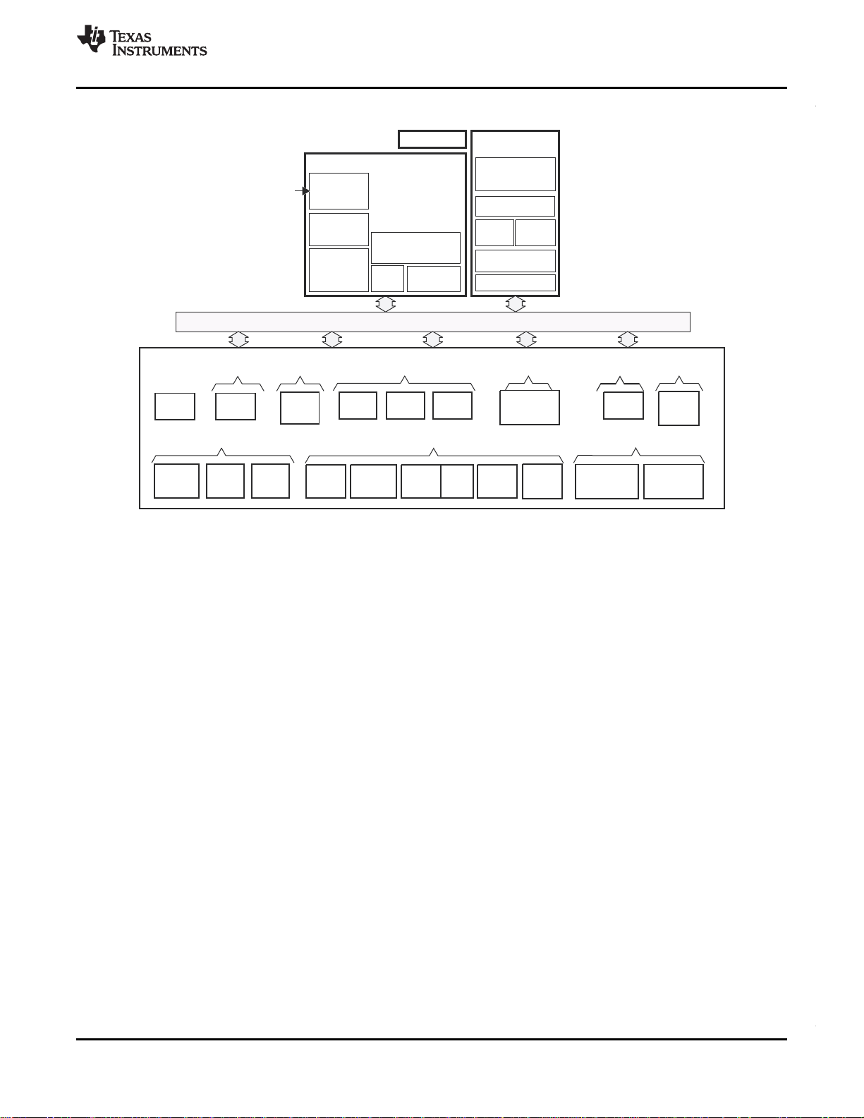
Switched Central Resource (SCR)
16 KB
I-Cache
16 KB
D-Cache
4 KB ETB
ARM926EJ-S CPU
With MMU
ARM Subsystem
JTAG Interface
System Control
Input
Clock(s)
64 KB ROM
8 KB RAM
(Vector Table)
Power/Sleep
Controller
Pin
Multiplexing
RTC/
32-KHz
OSC
PLL/Clock
Generator
w/OSC
GeneralPurpose
Timer
GeneralPurpose
Timer
(Watchdog)
Serial Interfaces
I C
(2)
2
SPI
(2)
UART
(3)
Audio Ports
McASP
w/FIFO
(3)
DMA
Peripherals
Display
Internal Memory
LCD
Ctlr
128 KB
RAM
External Memory Interfaces
Connectivity
EDMA3
Control Timers
eHRPWM
(3)
eCAP
(3)
eQEP
(2)
(10/100)
EMAC
(RMII)
MDIO
USB1.1
OHCI Ctlr
PHY
USB2.0
OTG Ctlr
PHY
HPI
MMC/SD
(8b)
EMIFA(8b/16B)
NAND/Flash
16b SDRAM
EMIFB
SDRAM Only
(16b/32b)
GPIO
Customizable Interface
PRU
Subsystem
AM1707
www.ti.com
1.4 Functional Block Diagram
SPRS637B–FEBRUARY 2010–REVISED AUGUST 2010
Copyright © 2010, Texas Instruments Incorporated AM1707 ARM Microprocessor 5
Submit Documentation Feedback
Product Folder Link(s): AM1707
Page 6

ADVANCEINFORMATION
AM1707
SPRS637B–FEBRUARY 2010–REVISED AUGUST 2010
1 AM1707 ARM Microprocessor ........................ 1
1.1 Features .............................................. 1 6.11 External Memory Interface A (EMIFA) ............. 66
1.2 Trademarks .......................................... 3
1.3 Description ........................................... 4
1.4 Functional Block Diagram ............................ 5
2 Revision History ......................................... 7
3 Device Overview ........................................ 8
3.1 Device Characteristics ............................... 8
3.2 Device Compatibility ................................. 9
3.3 ARM Subsystem ..................................... 9
3.4 Memory Map Summary ............................. 12
3.5 Pin Assignments .................................... 15
3.6 Terminal Functions ................................. 16
4 Device Configuration ................................. 34
4.1 Boot Modes ......................................... 34
4.2 SYSCFG Module ................................... 35
4.3 Pullup/Pulldown Resistors .......................... 37
5 Device Operating Conditions ....................... 38
5.1 Absolute Maximum Ratings Over Operating
Junction Temperature Range
(Unless Otherwise Noted) ................................. 38
5.2 Recommended Operating Conditions .............. 39
5.3 Notes on Recommended Power-On Hours (POH)
...................................................... 40
5.4 Electrical Characteristics Over Recommended
Ranges of Supply Voltage and Operating Junction
Temperature (Unless Otherwise Noted) ............ 41
6 Peripheral Information and Electrical
Specifications .......................................... 42
6.1 Parameter Information .............................. 42
6.2 Recommended Clock and Control Signal Transition
Behavior ............................................ 43
6.3 Power Supplies ..................................... 43
6.4 Unused USB0 (USB2.0) and USB1 (USB1.1) Pin
Configurations ...................................... 43
6.5 Reset ............................................... 45
6.6 Crystal Oscillator or External Clock Input .......... 48
6.7 Clock PLLs ......................................... 50
6.8 Interrupts ............................................ 54
6.9 General-Purpose Input/Output (GPIO) ............. 58
6.10 EDMA ............................................... 61
6.12 External Memory Interface B (EMIFB) ............. 75
6.13 Memory Protection Units ........................... 82
6.14 MMC / SD / SDIO (MMCSD) ....................... 85
6.15 Ethernet Media Access Controller (EMAC) ......... 88
6.16 Management Data Input/Output (MDIO) ........... 93
6.17 Multichannel Audio Serial Ports (McASP0, McASP1,
and McASP2) ....................................... 95
6.18 Serial Peripheral Interface Ports (SPI0, SPI1) .... 108
6.19 Enhanced Capture (eCAP) Peripheral ............ 126
6.20 Enhanced Quadrature Encoder (eQEP) Peripheral
..................................................... 129
6.21 Enhanced High-Resolution Pulse-Width Modulator
(eHRPWM) ........................................ 131
6.22 LCD Controller .................................... 135
6.23 Timers ............................................. 150
6.24 Inter-Integrated Circuit Serial Ports (I2C0, I2C1)
..................................................... 152
6.25 Universal Asynchronous Receiver/Transmitter
(UART) ............................................ 157
6.26 USB1 Host Controller Registers (USB1.1 OHCI)
..................................................... 159
6.27 USB0 OTG (USB2.0 OTG) ........................ 161
6.28 Host-Port Interface (UHPI) ........................ 169
6.29 Power and Sleep Controller (PSC) ................ 176
6.30 Programmable Real-Time Unit Subsystem (PRUSS)
..................................................... 179
6.31 Emulation Logic ................................... 182
6.32 IEEE 1149.1 JTAG ................................ 188
6.33 Real Time Clock (RTC) ........................... 190
7 Device and Documentation Support ............. 193
7.1 Device Support .................................... 193
7.2 Documentation Support ........................... 193
8 Mechanical Packaging and Orderable
Information ............................................ 194
8.1 Device and Development-Support Tool
Nomenclature ..................................... 194
8.2 Packaging Materials Information .................. 194
8.3 Thermal Data for ZKB ............................. 195
8.4 Mechanical Drawings ............................. 195
www.ti.com
6 Contents Copyright © 2010, Texas Instruments Incorporated
Submit Documentation Feedback
Product Folder Link(s): AM1707
Page 7
ADVANCEINFORMATION
AM1707
www.ti.com
SPRS637B–FEBRUARY 2010–REVISED AUGUST 2010
2 Revision History
This data manual revision history highlights the changes made to the SPRS637A device-specific data
manual to make it an SPRS637B revision.
Table 2-1. Revision History
ADDITIONS/MODIFICATIONS/DELETIONS
Global - Changed SPI td(SCSL_SPC)S min from P to 2P
Global - Replaced all "CLKIN" references with "OSCIN"
Global - Updated SPI Electrical parameters
Added Section 5.3, Notes on Recommended Power-On Hours (POH).
Section 6.5- Updated "All pins are tri-stated with the exception of RESETOUT which remains active through the reset sequence" to " All
pins are tri-stated with the exception of RESETOUT, which remains active through the reset sequence, and RTCK/GP7[14]. If an emulator
is driving TCK into the device during reset, then RTCK/GP7[14] will drive out RTCK. If TCK is not being driven into the device during reset,
then RTCK/GP7[14] will drive low."
Updated Warm Reset Timing Diagram - Figure 6-5
Updated the PLL diagram - Figure 6-9
Copyright © 2010, Texas Instruments Incorporated Revision History 7
Submit Documentation Feedback
Product Folder Link(s): AM1707
Page 8
ADVANCEINFORMATION
AM1707
SPRS637B–FEBRUARY 2010–REVISED AUGUST 2010
www.ti.com
3 Device Overview
3.1 Device Characteristics
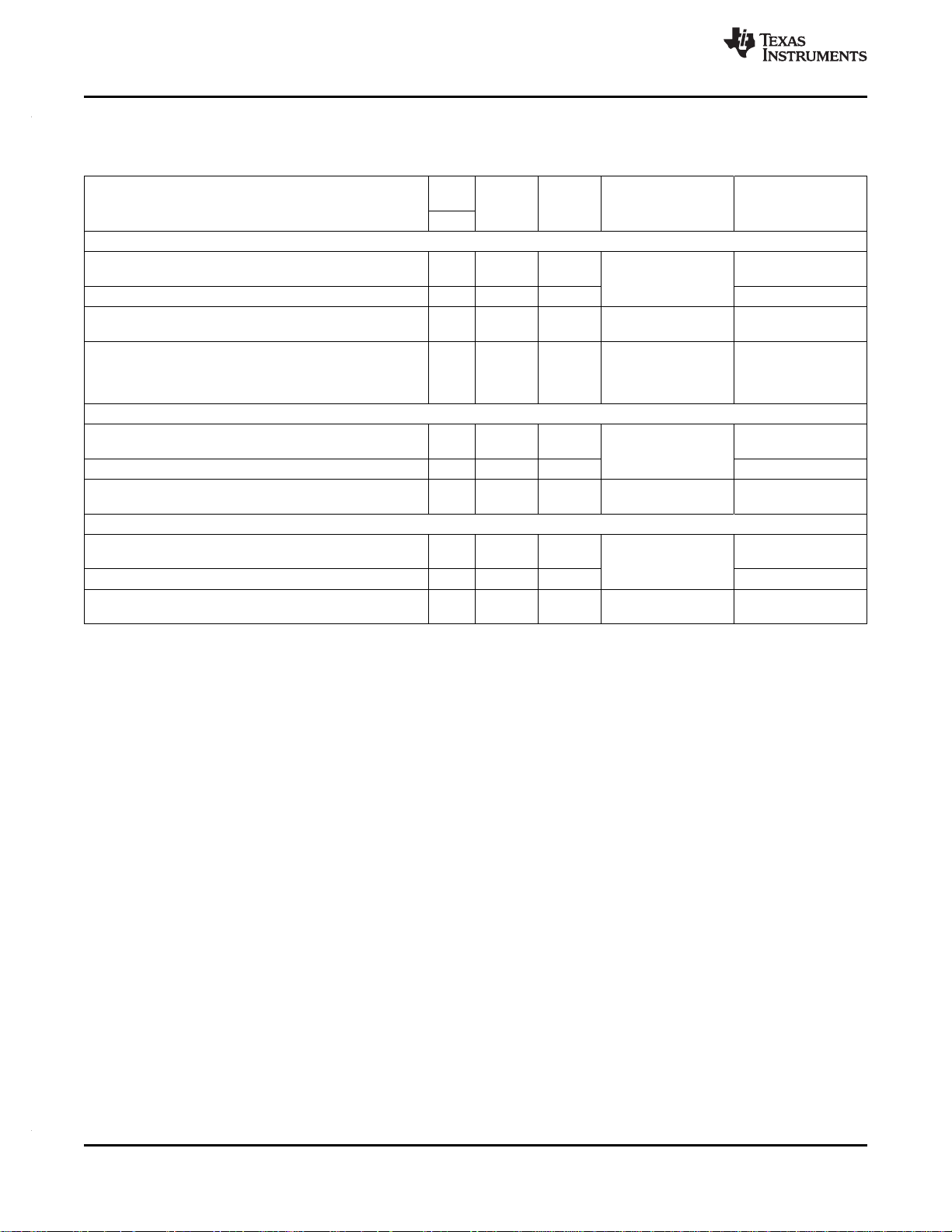
Table 3-1 provides an overview of the device . The table shows significant features of the device, including
the capacity of on-chip RAM, peripherals, and the package type with pin count.
Table 3-1. Characteristics of the device
HARDWARE FEATURES AM1707
EMIFB 16/32bit, upto 512Mb SDRAM
EMIFA Asynchronous (8/16-bit bus width) RAM, Flash, 16bit upto 128Mb SDRAM, NOR, NAND
Flash Card Interface MMC and SD cards supported.
EDMA3 32 independent channels, 8 QDMA channels, 2 Transfer controllers
Timers
UART 3 (one with RTS and CTS flow control)
SPI 2 (Each with one hardware chip select)
I2C 2 (both Master/Slave)
Peripherals
Not all peripherals pins
are available at the
same time (for more
detail, see the Device
Configurations section).
On-Chip Memory
JTAG BSDL_ID DEVIDR0 register
CPU Frequency MHz ARM926 375 MHz (1.2V) or 456 MHz (1.3V)
Voltage
Package 17 mm x 17 mm, 256-Ball 1 mm pitch, PBGA (ZKB)
Product Status
(1) ADVANCE INFORMATION concerns new products in the sampling or preproduction phase of development. Characteristic data and
other specifications are subject to change without notice.
(1)
Multichannel Audio
Serial Port [McASP]
10/100 Ethernet MAC
with Management Data 1 (RMII Interface)
I/O
eHRPWM 6 Single Edge, 6 Dual Edge Symmetric, or 3 Dual Edge Asymmetric Outputs
eCAP 3 32-bit capture inputs or 3 32-bit auxiliary PWM outputs
eQEP 2 32-bit QEP channels with 4 inputs/channel
UHPI 1 (16-bit multiplexed address/data)
USB 2.0 (USB0) High-Speed OTG Controller with on-chip OTG PHY
USB 1.1 (USB1) Full-Speed OHCI (as host) with on-chip PHY
General-Purpose
Input/Output Port
PRU Subsystem
(PRUSS)
LCD Controller 1
Size (Bytes) 168KB RAM, 64KB ROM
Organization
Core (V)
I/O (V) 3.3 V
Product Preview (PP),
Advance Information
(AI),
or Production Data
(PD)
2 64-Bit General Purpose (configurable as 2 separate 32-bit timers, 1 configurable as
Watch Dog)
3 (each with transmit/receive, FIFO buffer, 16/12/4 serializers)
8 banks of 16-bit
2 Programmable PRU Cores
ARM
16KB I-Cache
16KB D-Cache
8KB RAM (Vector Table)
64KB ROM
ADDITIONAL MEMORY
128KB RAM
0x8B7D F02F (Silicon Revision 1.1)
0x9B7D F02F (Silicon Revision 2.0)
1.2 V nominal for 375 MHz version
1.3 V nominal for 456 MHz version
375 MHz Versions -PD
456 MHz Version - AI
8 Device Overview Copyright © 2010, Texas Instruments Incorporated
Submit Documentation Feedback
Product Folder Link(s): AM1707
Page 9

ADVANCEINFORMATION
AM1707
www.ti.com
3.2 Device Compatibility
The ARM926EJ-S RISC CPU is compatible with other ARM9 CPUs from ARM Holdings plc.
3.3 ARM Subsystem
The ARM Subsystem includes the following features:
• ARM926EJ-S RISC processor
• ARMv5TEJ (32/16-bit) instruction set
• Little endian
• System Control Co-Processor 15 (CP15)
• MMU
• 16KB Instruction cache
• 16KB Data cache
• Write Buffer
• Embedded Trace Module and Embedded Trace Buffer (ETM/ETB)
• ARM Interrupt controller
3.3.1 ARM926EJ-S RISC CPU
The ARM Subsystem integrates the ARM926EJ-S processor. The ARM926EJ-S processor is a member of
ARM9 family of general-purpose microprocessors. This processor is targeted at multi-tasking applications
where full memory management, high performance, low die size, and low power are all important. The
ARM926EJ-S processor supports the 32-bit ARM and 16 bit THUMB instruction sets, enabling the user to
trade off between high performance and high code density. Specifically, the ARM926EJ-S processor
supports the ARMv5TEJ instruction set, which includes features for efficient execution of Java byte codes,
providing Java performance similar to Just in Time (JIT) Java interpreter, but without associated code
overhead.
SPRS637B–FEBRUARY 2010–REVISED AUGUST 2010
The ARM926EJ-S processor supports the ARM debug architecture and includes logic to assist in both
hardware and software debug. The ARM926EJ-S processor has a Harvard architecture and provides a
complete high performance subsystem, including:
• ARM926EJ -S integer core
• CP15 system control coprocessor
• Memory Management Unit (MMU)
• Separate instruction and data caches
• Write buffer
• Separate instruction and data (internal RAM) interfaces
• Separate instruction and data AHB bus interfaces
• Embedded Trace Module and Embedded Trace Buffer (ETM/ETB)
For more complete details on the ARM9, refer to the ARM926EJ-S Technical Reference Manual, available
at http://www.arm.com
3.3.2 CP15
The ARM926EJ-S system control coprocessor (CP15) is used to configure and control instruction and
data caches, Memory Management Unit (MMU), and other ARM subsystem functions. The CP15 registers
are programmed using the MRC and MCR ARM instructions, when the ARM in a privileged mode such as
supervisor or system mode.
Copyright © 2010, Texas Instruments Incorporated Device Overview 9
Submit Documentation Feedback
Product Folder Link(s): AM1707
Page 10

ADVANCEINFORMATION
AM1707
SPRS637B–FEBRUARY 2010–REVISED AUGUST 2010
3.3.3 MMU
A single set of two level page tables stored in main memory is used to control the address translation,
permission checks and memory region attributes for both data and instruction accesses. The MMU uses a
single unified Translation Lookaside Buffer (TLB) to cache the information held in the page tables. The
MMU features are:
• Standard ARM architecture v4 and v5 MMU mapping sizes, domains and access protection scheme.
• Mapping sizes are:
– 1MB (sections)
– 64KB (large pages)
– 4KB (small pages)
– 1KB (tiny pages)
• Access permissions for large pages and small pages can be specified separately for each quarter of
the page (subpage permissions)
• Hardware page table walks
• Invalidate entire TLB, using CP15 register 8
• Invalidate TLB entry, selected by MVA, using CP15 register 8
• Lockdown of TLB entries, using CP15 register 10
3.3.4 Caches and Write Buffer
The size of the Instruction cache is 16KB, Data cache is 16KB. Additionally, the caches have the following
features:
• Virtual index, virtual tag, and addressed using the Modified Virtual Address (MVA)
• Four-way set associative, with a cache line length of eight words per line (32-bytes per line) and with
two dirty bits in the Dcache
• Dcache supports write-through and write-back (or copy back) cache operation, selected by memory
region using the C and B bits in the MMU translation tables
• Critical-word first cache refilling
• Cache lockdown registers enable control over which cache ways are used for allocation on a line fill,
providing a mechanism for both lockdown, and controlling cache corruption
• Dcache stores the Physical Address TAG (PA TAG) corresponding to each Dcache entry in the TAG
RAM for use during the cache line write-backs, in addition to the Virtual Address TAG stored in the
TAG RAM. This means that the MMU is not involved in Dcache write-back operations, removing the
possibility of TLB misses related to the write-back address.
• Cache maintenance operations provide efficient invalidation of, the entire Dcache or Icache, regions of
the Dcache or Icache, and regions of virtual memory.
www.ti.com
The write buffer is used for all writes to a noncachable bufferable region, write-through region and write
misses to a write-back region. A separate buffer is incorporated in the Dcache for holding write-back for
cache line evictions or cleaning of dirty cache lines. The main write buffer has 16-word data buffer and a
four-address buffer. The Dcache write-back has eight data word entries and a single address entry.
3.3.5 Advanced High-Performance Bus (AHB)
The ARM Subsystem uses the AHB port of the ARM926EJ-S to connect the ARM to the Config bus and
the external memories. Arbiters are employed to arbitrate access to the separate D-AHB and I-AHB by the
Config Bus and the external memories bus.
3.3.6 Embedded Trace Macrocell (ETM) and Embedded Trace Buffer (ETB)
To support real-time trace, the ARM926EJ-S processor provides an interface to enable connection of an
Embedded Trace Macrocell (ETM). The ARM926EJ-S Subsystem in the device also includes the
Embedded Trace Buffer (ETB). The ETM consists of two parts:
10 Device Overview Copyright © 2010, Texas Instruments Incorporated
Submit Documentation Feedback
Product Folder Link(s): AM1707
Page 11

ADVANCEINFORMATION
AM1707
www.ti.com
• Trace Port provides real-time trace capability for the ARM9.
• Triggering facilities provide trigger resources, which include address and data comparators, counter,
and sequencers.
The device trace port is not pinned out and is instead only connected to the Embedded Trace Buffer. The
ETB has a 4KB buffer memory. ETB enabled debug tools are required to read/interpret the captured trace
data.
This device uses ETM9™ version r2p2 and ETB version r0p1. Documentation on the ETM and ETB is
available from ARM Ltd. Reference the ' CoreSight™ ETM9™ Technical Reference Manual, revision r0p1'
and the 'ETM9 Technical Reference Manual, revision r2p2'.
3.3.7 ARM Memory Mapping
By default the ARM has access to most on and off chip memory areas, EMIFA, EMIFB, and the additional
128K byte on chip SRAM. Likewise almost all of the on chip peripherals are accessible to the ARM by
default.
See Table 3-2 for a detailed top level device memory map that includes the ARM memory space.
SPRS637B–FEBRUARY 2010–REVISED AUGUST 2010
Copyright © 2010, Texas Instruments Incorporated Device Overview 11
Submit Documentation Feedback
Product Folder Link(s): AM1707
Page 12
ADVANCEINFORMATION
AM1707
SPRS637B–FEBRUARY 2010–REVISED AUGUST 2010
www.ti.com
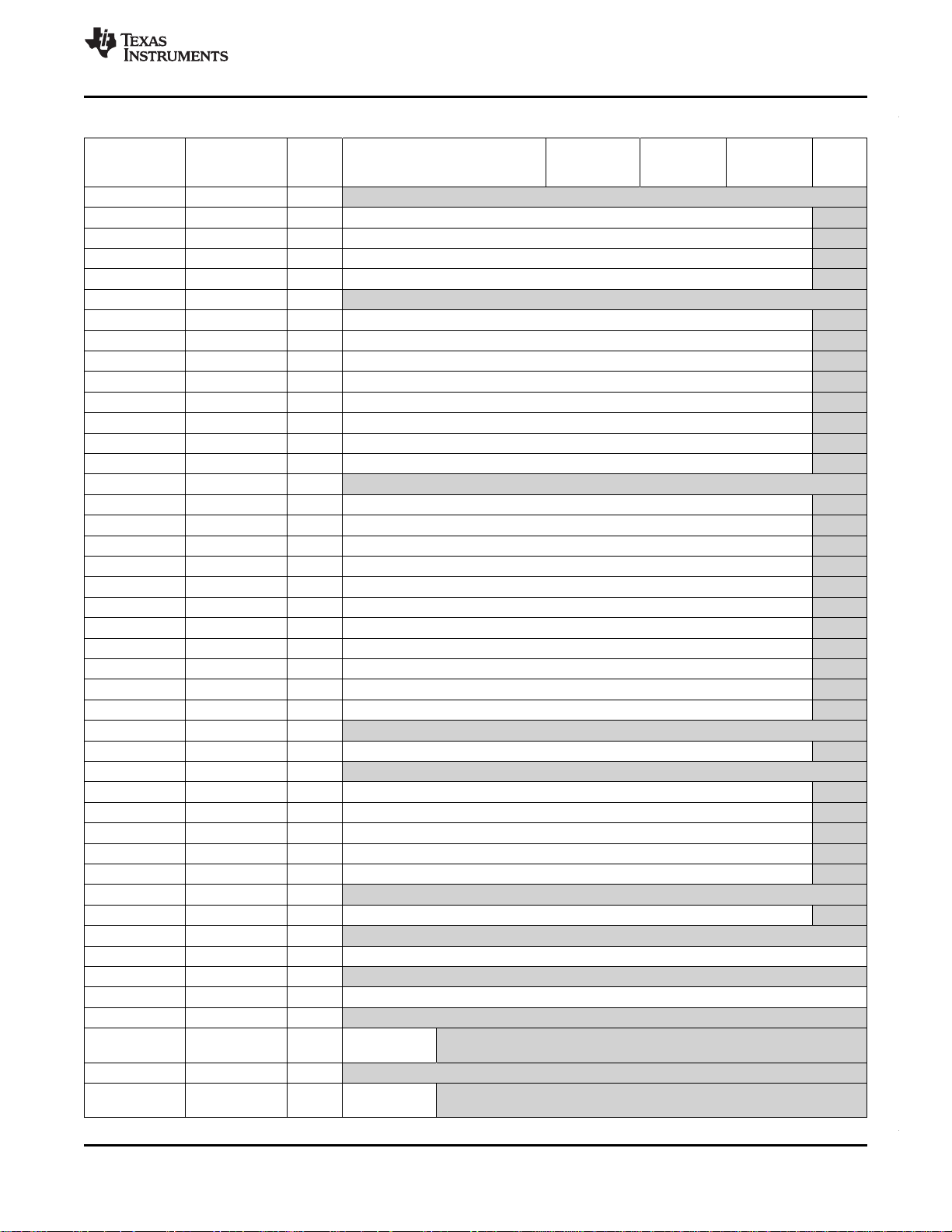
3.4 Memory Map Summary
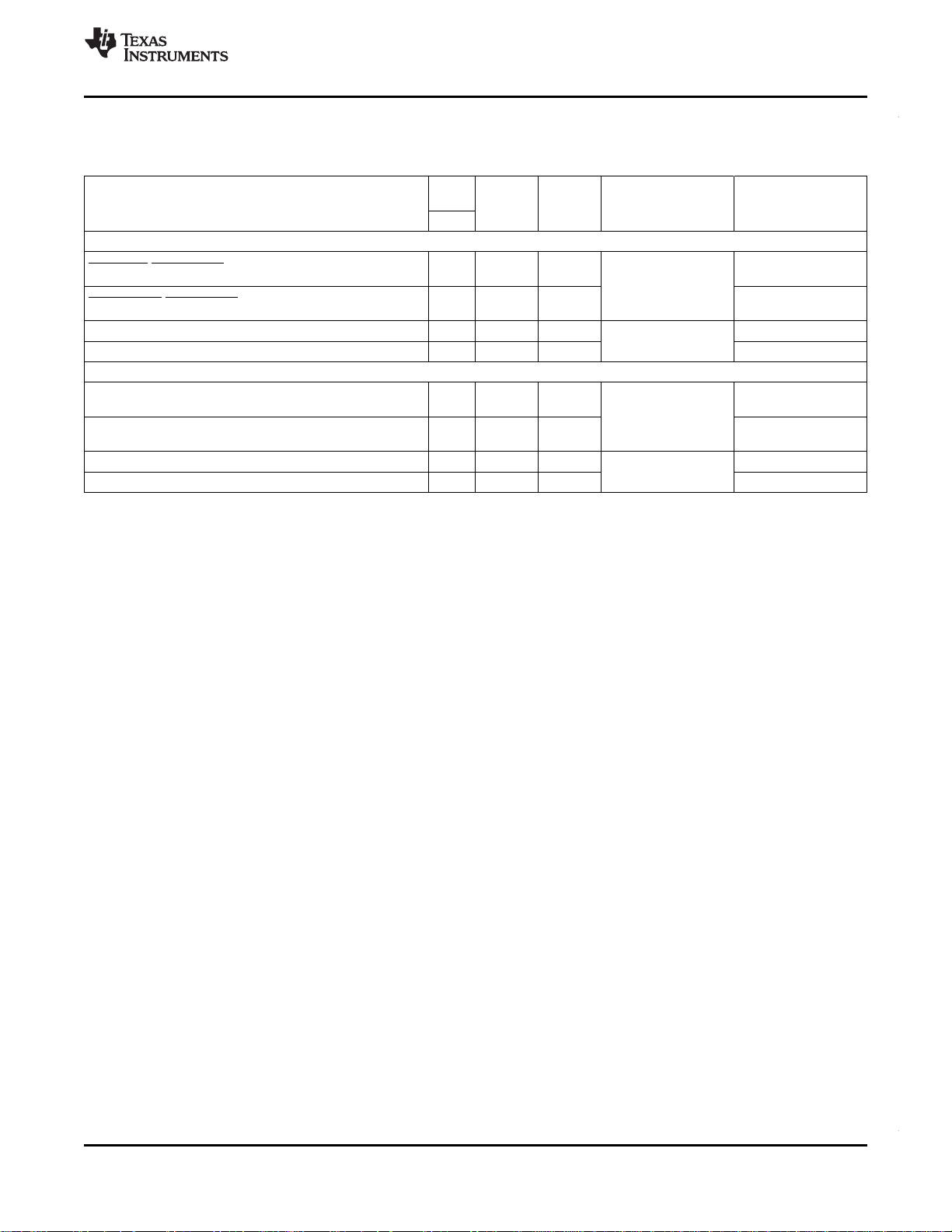
Table 3-2. AM1707 Top Level Memory Map
Start Address End Address Size ARM Mem Map EDMA Mem PRUSS Mem Master LCDC
0x0000 0000 0x0000 0FFF 4K - PRUSS Local
0x0000 1000 0x01BB FFFF
0x01BC 0000 0x01BC 0FFF 4K ARM ETB -
memory
0x01BC 1000 0x01BC 17FF 2K ARM ETB reg 0x01BC 1800 0x01BC 18FF 256 ARM Ice -
Crusher
0x01BC 1900 0x01BF FFFF 0x01C0 0000 0x01C0 7FFF 32K EDMA3 Channel Controller 0x01C0 8000 0x01C0 83FF 1024 EDMA3 Transfer Controller 0 0x01C0 8400 0x01C0 87FF 1024 EDMA3 Transfer Controller 1 0x01C0 8800 0x01C0 FFFF 0x01C1 0000 0x01C1 0FFF 4K PSC 0 0x01C1 1000 0x01C1 1FFF 4K PLL Controller 0x01C1 2000 0x01C1 3FFF 0x01C1 4000 0x01C1 4FFF 4K SYSCFG 0x01C1 5000 0x01C1 FFFF 0x01C2 0000 0x01C2 0FFF 4K Timer64P 0 0x01C2 1000 0x01C2 1FFF 4K Timer64P 1 0x01C2 2000 0x01C2 2FFF 4K I2C 0 0x01C2 3000 0x01C2 3FFF 4K RTC 0x01C2 4000 0x01C3 FFFF - 0x01C4 0000 0x01C4 0FFF 4K MMC/SD 0 0x01C4 1000 0x01C4 1FFF 4K SPI 0 0x01C4 2000 0x01C4 2FFF 4K UART 0 0x01C4 3000 0x01CF FFFF 0x01D0 0000 0x01D0 0FFF 4K McASP 0 Control 0x01D0 1000 0x01D0 1FFF 4K McASP 0 AFIFO Control 0x01D0 2000 0x01D0 2FFF 4K McASP 0 Data 0x01D0 3000 0x01D0 3FFF 0x01D0 4000 0x01D0 4FFF 4K McASP 1 Control 0x01D0 5000 0x01D0 5FFF 4K McASP 1 AFIFO Control 0x01D0 6000 0x01D0 6FFF 4K McASP 1 Data 0x01D0 7000 0x01D0 7FFF 0x01D0 8000 0x01D0 8FFF 4K McASP 2 Control 0x01D0 9000 0x01D0 9FFF 4K McASP 2 AFIFO Control 0x01D0 A000 0x01D0 AFFF 4K McASP 2 Data 0x01D0 B000 0x01D0 BFFF 0x01D0 C000 0x01D0 CFFF 4K UART 1 0x01D0 D000 0x01D0 DFFF 4K UART 2 0x01D0 E000 0x01DF FFFF - -
0x01E0 0000 0x01E0 FFFF 64K USB0 0x01E1 0000 0x01E1 0FFF 4K UHPI -
Map Map Peripheral Mem
Mem Map Map
Address
Space
12 Device Overview Copyright © 2010, Texas Instruments Incorporated
Submit Documentation Feedback
Product Folder Link(s): AM1707
Page 13
ADVANCEINFORMATION
AM1707
www.ti.com
SPRS637B–FEBRUARY 2010–REVISED AUGUST 2010
Table 3-2. AM1707 Top Level Memory Map (continued)
Start Address End Address Size ARM Mem Map EDMA Mem PRUSS Mem Master LCDC
0x01E1 1000 0x01E1 1FFF 0x01E1 2000 0x01E1 2FFF 4K SPI 1 0x01E1 3000 0x01E1 3FFF 4K LCD Controller 0x01E1 4000 0x01E1 4FFF 4K Memory Protection Unit 1 (MPU 1) 0x01E1 5000 0x01E1 5FFF 4K Memory Protection Unit 2 (MPU 2) 0x01E1 6000 0x01E1 FFFF 0x01E2 0000 0x01E2 1FFF 8K EMAC Control Module RAM 0x01E2 2000 0x01E2 2FFF 4K EMAC Control Module Registers 0x01E2 3000 0x01E2 3FFF 4K EMAC Control Registers 0x01E2 4000 0x01E2 4FFF 4K EMAC MDIO port 0x01E2 5000 0x01E2 5FFF 4K USB1 0x01E2 6000 0x01E2 6FFF 4K GPIO 0x01E2 7000 0x01E2 7FFF 4K PSC 1 0x01E2 8000 0x01E2 8FFF 4K I2C 1 0x01E2 9000 0x01EF FFFF 0x01F0 0000 0x01F0 0FFF 4K eHRPWM 0 0x01F0 1000 0x01F0 1FFF 4K HRPWM 0 0x01F0 2000 0x01F0 2FFF 4K eHRPWM 1 0x01F0 3000 0x01F0 3FFF 4K HRPWM 1 0x01F0 4000 0x01F0 4FFF 4K eHRPWM 2 0x01F0 5000 0x01F0 5FFF 4K HRPWM 2 0x01F0 6000 0x01F0 6FFF 4K ECAP 0 0x01F0 7000 0x01F0 7FFF 4K ECAP 1 0x01F0 8000 0x01F0 8FFF 4K ECAP 2 -
0x01F0 9000 0x01F0 9FFF 4K EQEP 0 0x01F0 A000 0x01F0 AFFF 4K EQEP 1 0x01F0 B000 0x3FFF FFFF -
0x4000 0000 0x47FF FFFF 128M EMIFA SDRAM data (CS0) -
0x4800 0000 0x5FFF FFFF
0x6000 0000 0x61FF FFFF 32M EMIFA async data (CS2) -
0x6200 0000 0x63FF FFFF 32M EMIFA async data (CS3) -
0x6400 0000 0x65FF FFFF 32M EMIFA async data (CS4) -
0x6600 0000 0x67FF FFFF 32M EMIFA async data (CS5) -
0x6800 0000 0x6800 7FFF 32K EMIFA Control Registers -
0x6800 8000 0x7FFF FFFF -
0x8000 0000 0x8001 FFFF 128K On-chip RAM -
0x8002 0000 0xAFFF FFFF -
0xB000 0000 0xB000 7FFF 32K EMIFB Control Registers
0xB000 8000 0xBFFF FFFF 0xC000 0000 0xCFFF FFFF 256M EMIFB SDRAM Data
0xD000 0000 0xFFFC FFFF
0xFFFD 0000 0xFFFD FFFF 64K ARM local -
ROM
0xFFFE 0000 0xFFFE DFFF 0xFFFE E000 0xFFFE FFFF 8K ARM Interrupt -
Controller
Map Map Peripheral Mem
Mem Map Map
Copyright © 2010, Texas Instruments Incorporated Device Overview 13
Submit Documentation Feedback
Product Folder Link(s): AM1707
Page 14

ADVANCEINFORMATION
AM1707
SPRS637B–FEBRUARY 2010–REVISED AUGUST 2010
www.ti.com
Table 3-2. AM1707 Top Level Memory Map (continued)
Start Address End Address Size ARM Mem Map EDMA Mem PRUSS Mem Master LCDC
0xFFFF 0000 0xFFFF 1FFF 8K ARM local - ARM local
RAM RAM (PRU 0
0xFFFF 2000 0xFFFF FFFF -
Map Map Peripheral Mem
Mem Map Map
Only)
14 Device Overview Copyright © 2010, Texas Instruments Incorporated
Submit Documentation Feedback
Product Folder Link(s): AM1707
Page 15
ADVANCEINFORMATION
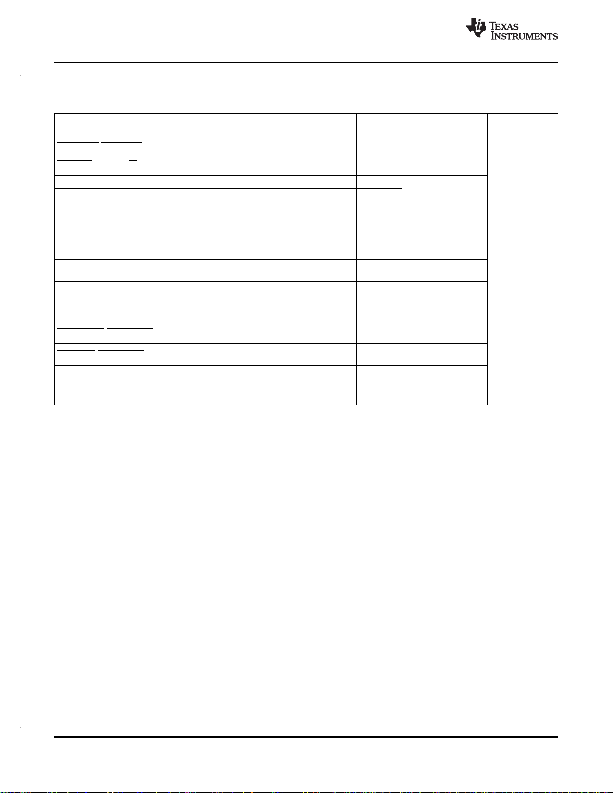
V
SS
V
SS
T
AXR1[0]/
GP4[0]
AXR1[11]/
GP5[11]
SPI0_CLK/
EQEP1I/
GP5[2]/
BOOT[2]
SPI1_CLK/
EQEP1S/
GP5[7]/
BOOT[7]
1 2 3 4 5 6
EMA_CS[3]/
AMUTE2/
GP2[6]
7
EMA_CS[0]
UHPI_HAS//
GP2[4]
8
EMA_A[0]/
LCD_D[7]/
GP1[0]
9
EMA_A[4]/
LCD_D[3]/
GP1[4]
10
EMA_A[8]/
LCD_PCLK/
GP1[8]
11
EMA_SDCKE/
GP2[0]
12
EMA_D[0]/
MMCSD_DAT[0]/
UHPI_HD[0]/
GP0[0]/
BOOT[12]
13
EMA_D[9]/
UHPI_HD[9]/
LCD_D[9]/
GP0[9]
14
V
SS
V
SS
15 16
DV
DD
R
AXR1[1]/
GP4[1]
UART0_RXD/
I2C0_SDA/
TM64P0_IN12/
GP5[8]/
BOOT[8]
SPI1_ENA/
UART2_RXD/
GP5[12]
SPI0_ENA
UART0_CTS//
EQEP0A/
GP5[3]/
BOOT[3]
SPI0_SOMI[0]/
EQEP0I/
GP5[0]/
BOOT[0]
EMA_OE
UHPI_HDS1//
AXR0[13]/
GP2[7]
EMA_BA[0]/
LCD_D[4]/
GP1[14]
EMA_A[1]/
MMCSD_CLK/
UHPI_HCNTL0/
GP1[1]
EMA_A[5]/
LCD_D[2]/
GP1[5]
EMA_A[9]/
LCD_HSYNC/
GP1[9]
EMA_CLK/
OBSCLK/
AHCLKR2/
GP1[15]
EMA_D[2]/
MMCSD_DAT[2]/
UHPI_HD[2]/
GP0[2]
EMA_D[10]/
UHPI_HD[10]/
LCD_D[10]/
GP0[10]
EMA_D[1]/
MMCSD_DAT[1]/
UHPI_HD[1]/
GP0[1]
DV
DD
P
AXR1[3]/
EQEP1A/
GP4[3]
AXR1[2]/
GP4[2]
UART0_TXD/
I2C0_SCL/
TM64P0_OUT12/
GP5[9]/
BOOT[9]
SPI1_SCS[0]/
UART2_TXD/
GP5[13]
SPI1_SOMI[0]/
I2C1_SCL/
GP5[5]/
BOOT[5]
SPI0_SIMO[0]/
EQEP0S/
GP5[1]/
BOOT[1]
EMA_CS[2]
UHPI_HCS//
GP2[5]/
BOOT[15]
EMA_BA[1]/
LCD_D[5]/
UHPI_HHWIL/
GP1[13]
EMA_A[2]/
MMCSD_CMD/
UHPI_HCNTL1/
GP1[2]
EMA_A[6]/
LCD_D[1]/
GP1[6]
EMA_A[11]/
/
GP1[11]
LCD_AC_
ENB_CS
EMA_WE_
DQM[1]
UHPI_HDS2//
AXR0[14]/
GP2[8]
EMA_D[4]/
MMCSD_DAT[4]/
UHPI_HD[4]/
GP0[4]
EMA_D[12]/
UHPI_HD[12]/
LCD_D[12]/
GP0[12]
EMA_D[3]/
MMCSD_DAT[3]/
UHPI_HD[3]/
GP0[3]
EMA_D[11]/
UHPI_HD[11]/
LCD_D[11]
GP0[11]
N
AXR1[5]/
EPWM2B/
GP4[5]
AXR1[4]/
EQEP1B/
GP4[4]
AXR1[10]/
GP5[10]
SPI0_SCS[0]
UART0_RTS//
EQEP0B/
GP5[4]/
BOOT[4]
SPI1_SIMO[0]/
I2C1_SDA/
GP5[6]/
BOOT[6]
EMA_WAIT[0]/
/
GP2[10]
UHPI_HRDY
EMA_RAS/
EMA_CS[5]/
GP2[2]
EMA_A[10]/
LCD_VSYNC/
GP1[10]
EMA_A[3]/
LCD_D[6]/
GP1[3]
EMA_A[7]/
LCD_D[0]/
GP1[7]
EMA_A[12]/
LCD_MCLK/
GP1[12]
EMA_D[8]/
UHPI_HD[8]/
LCD_D[8]/
GP0[8]
EMA_D[6]/
MMCSD_DAT[6]/
UHPI_HD[6]/
GP0[6]
EMA_D[14]/
UHPI_HD[14]/
LCD_D[14]/
GP0[14]
EMA_D[5]/
MMCSD_DAT[5]/
UHPI_HD[5]/
GP0[5]
EMA_D[13]/
UHPI_HD[13]/
LCD_D[13]/
GP0[13]
M
AXR1[9]/
GP4[9]
AXR1[8]/
EPWM1A/
GP4[8]
AXR1[7]/
EPWM1B/
GP4[7]
AXR1[6]/
EPWM2A/
GP4[6]
DV
DD
V
SS
V
SS
DV
DD
DV
DD
V
SS
V
SS
DV
DD
EMA_WEW/
UHPI_HR /
AXR0[12]/
GP2[3]/
BOOT[14]]
EMA_WE_
DQM[0]
UHPI_HINT//
AXR0[15]/
GP2[9]
EMA_D[7]/
MMCSD_DAT[7]/
UHPI_HD[7]/
GP0[7]/
BOOT[13]
EMA_D[15]/
UHPI_HD[15]/
LCD_D[15]/
GP0[15]
L
AHCLKR1/
GP4[11]
ACLKR1/
ECAP2/
APWM2/
GP4[12]
AFSR1/
GP4[13]
AMUTE0/
RESETOUT
DV
DD
CV
DD
V
SS
V
SS
V
SS
V
SS
DV
DD
DVDDEMB_CAS EMB_D[22] EMB_D[23]
EMA_CAS
EMA_CS[4]//
GP2[1]
K
RTCK/GP7[14]
AHCLKX1/
EPWM0B/
GP3[14]
ACLKX1/
EPWM0A/
GP3[15]
AFSX1/
EPWMSYNCI/
EPWMSYNCO/
GP4[10]
DV
DD
CV
DD
V
SS
V
SS
CV
DD
CV
DD
DVDDEMB_D[20]
EMB_WE_
DQM[0]/
GP5[15]
EMB_WE EMB_D[21]CV
DD
TMS
J
TDI
TDO TRST
EMU0/GP7[15]
CV
DD
CV
DD
V
SS
V
SS
CV
DD
CV
DD
CV
DD
EMB_D[5]/
GP6[5]
EMB_D[19]
EMB_D[6]/
GP6[6]
EMB_D[7]/
GP6[7]
RTC_XI
H
RTC_XO
TCK
NC
USB0_
VDDA33
CV
DD
V
SS
V
SS
CV
DD
CV
DD
EMB_D[3]/
GP6[3]
EMB_D[17] EMB_D[18]
EMB_D[4]/
GP6[4]
RTC_CV
DD
G
RTC_V
SS
RESET USB0_DM
DV
DD
CV
DD
V
SS
V
SS
CV
DD
CV
DD
DV
DD
CV
DD
EMB_D[1]/
GP6[1]
EMB_D[31] EMB_D[16]
EMB_D[2]/
GP6[2]
OSCOUT
F
OSCIN
NC USB0_DP
DV
DD
CV
DD
RSV1
V
SS
V
SS
V
SS
DV
DD
DV
DD
EMB_D[15]/
GP6[15]
EMB_D[29] EMB_D[30]
EMB_D[0]/
GP6[0]
PLL0_VSSA
E
OSCVSS
USB0_
VDDA18
USB0_
DRVVBUS/
GP4[15]
DV
DD
V
SS
V
SS
DV
DD
V
SS
V
SS
DV
DD
DV
DD
EMB_D[13]/
GP6[13]
EMB_D[27] EMB_D[28]
EMB_D[14]/
GP6[14]
PLL0_VDDA
D
USB0_ID
USB0_VBUS
AMUTE1/
EHRPWMTZ/
GP4[14]
AFSX0/
GP2[13]/
BOOT[10]
UART1_TXD/
AXR0[10]/
GP3[10]
AXR0[6]/
RMII_RXER/
ACLKR2/
GP3[6]
AXR0[2]/
RMII_TXEN/
AXR2[3]/
GP3[2]
EMB_CS[0]
EMB_A[0]/
GP7[2]
EMB_A[4]/
GP7[6]
EMB_A[8]/
GP7[10]
EMB_D[9]/
GP6[9]
EMB_D[10]/
GP6[10]
EMB_D[11]/
GP6[11]
EMB_D[12]/
GP6[12]
USB1_
VDDA33
C
USB1_
VDDA18
USB0_
VDDA12
AFSR0/
GP3[12]
ACLKX0/
ECAP0/
APWM0/
GP2[12]
UART1_RXD/
AXR0[9]/
GP3[9]
AXR0[5]/
RMII_RXD[1]/
AFSX2/
GP3[5]
AXR0[1]/
RMII_TXD[1]/
ACLKX2/
GP3[1]
EMB_BA[0]/
GP7[1]
EMB_A[1]/
GP7[3]
EMB_A[5]/
GP7[7]
EMB_A[9]/
GP7[11]
EMB_SDCKE EMB_CLK
EMB_WE_
DQM[1]/
GP5[14]
EMB_D[8]/
GP6[8]
B
RSV2 VSSUSB1_DM
ACLKR0/
ECAP1/
APWM1/
GP2[15]
AHCLKX0/
AHCLKX2/
USB_
REFCLKIN/
GP2[11]
AXR0[8]/
MDIO_D/
GP3[8]
AXR0[4]/
RMII_RXD[0]/
AXR2[1]/
GP3[4]
AXR0[0]/
RMII_TXD[0]/
AFSR2/
GP3[0]
1 2 3 4 5 6 7 8 9 10 11 12 13 14 15 16
EMB_BA[1]/
GP7[0]
EMB_A[2]/
GP7[4]
EMB_A[6]/
GP7[8]
EMB_A[11]/
GP7[13]
EMB_WE_
DQM[2]
EMB_D[25]
EMB_A[12]/
GP3[13]
DV
DD
A
V
SS
V
SS
USB1_DP
AHCLKR0/
RMII_MHZ_
50_CLK/
GP2[14]/
BOOT[11]
AXR0[11]/
AXR2[0]/
GP3[11]
AXR0[7]/
MDIO_CLK/
GP3[7]
AXR0[3]/
RMII_CRS_DV/
AXR2[2]/
GP3[3]
EMB_RAS
EMB_A[10]/
GP7[12]
EMB_A[3]/
GP7[5]
EMB_A[7]/
GP7[9]
EMB_WE_
DQM[3]
EMB_D[24] EMB_D[26] V
SS
V
SS
T
R
P
N
M
L
K
J
H
G
F
E
D
C
B
A
RV
DD
RV
DD
AM1707
www.ti.com
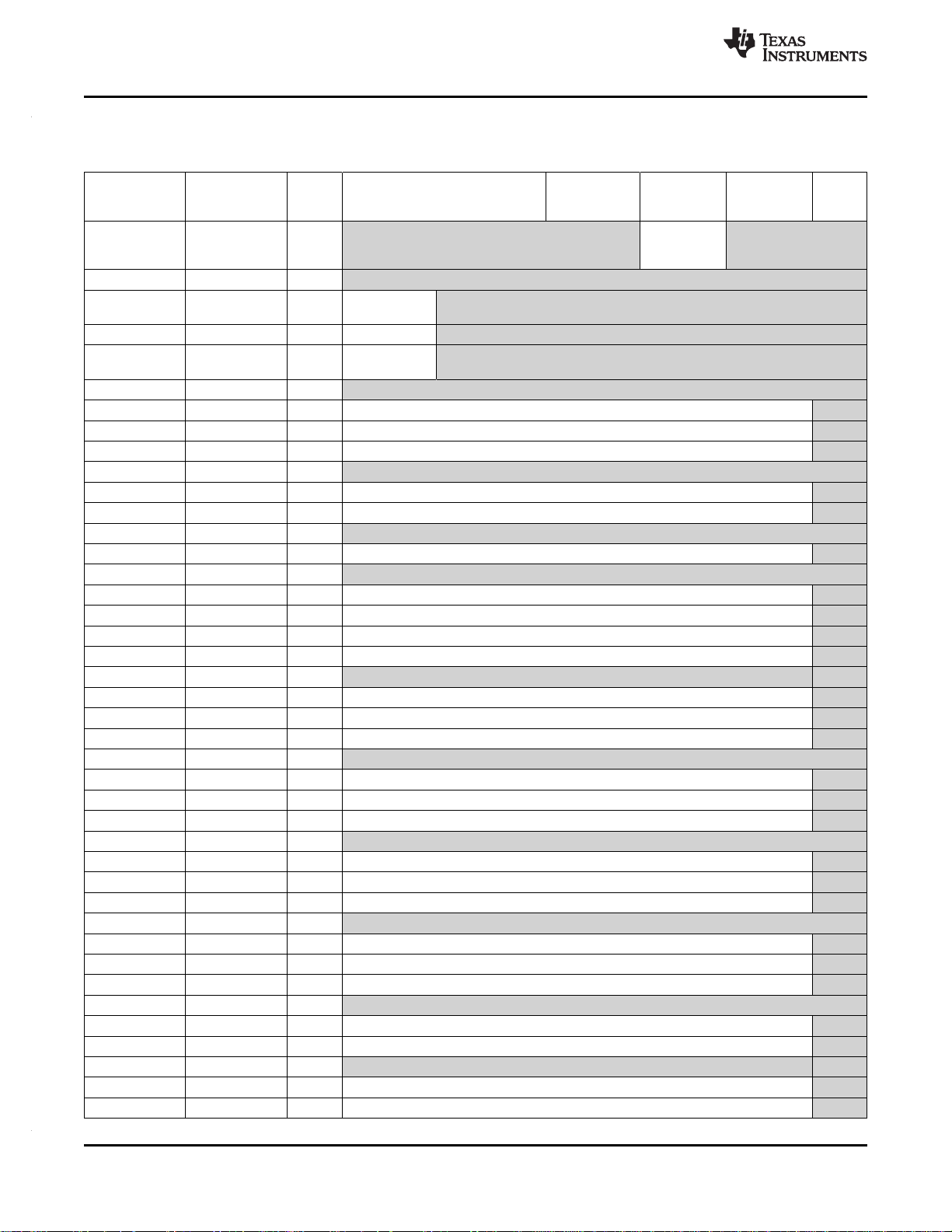
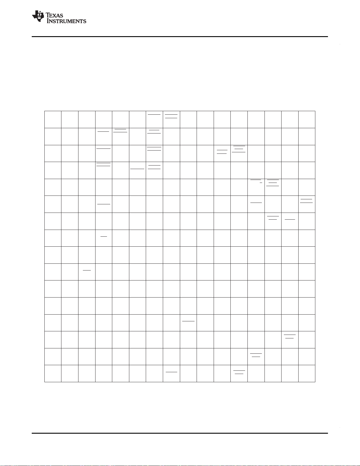
3.5 Pin Assignments
Extensive use of pin multiplexing is used to accommodate the largest number of peripheral functions in
the smallest possible package. Pin multiplexing is controlled using a combination of hardware
configuration at device reset and software programmable register settings.
3.5.1 Pin Map (Bottom View)
Figure 3-1 shows the pin assignments for the ZKB package.
SPRS637B–FEBRUARY 2010–REVISED AUGUST 2010
Copyright © 2010, Texas Instruments Incorporated Device Overview 15
Figure 3-1. Pin Map (ZKB)
Submit Documentation Feedback
Product Folder Link(s): AM1707
Page 16
ADVANCEINFORMATION
AM1707
SPRS637B–FEBRUARY 2010–REVISED AUGUST 2010
3.6 Terminal Functions
Table 3-3 to Table 3-23 identify the external signal names, the associated pin/ball numbers along with the
mechanical package designator, the pin type (I, O, IO, OZ, or PWR), whether the pin/ball has any internal
pullup/pulldown resistors, whether the pin/ball is configurable as an IO in GPIO mode, and a functional pin
description.
3.6.1 Device Reset and JTAG
Table 3-3. Reset and JTAG Terminal Functions
SIGNAL NAME TYPE
RESET G3 I Device reset input
AMUTE0/ RESETOUT L4 O
TMS J1 I IPU JTAG test mode select
TDI J2 I IPU JTAG test data input
TDO J3 O IPD JTAG test data output
TCK H3 I IPU JTAG test clock
TRST J4 I IPD JTAG test reset
EMU[0]/GP7[15] J5 I/O IPU Emulation Signal
RTCK/GP7[14] K1 I/O IPD JTAG Test Clock Return Clock Output
(1) I = Input, O = Output, I/O = Bidirectional, Z = High impedance, PWR = Supply voltage, GND = Ground, A = Analog signal.
Note: For multiplexed pins where functions have different types (ie., input versus output), the table reflects the pin function direction for
that particular peripheral.
(2) IPD = Internal Pulldown resistor, IPU = Internal Pullup resistor
(3) Open drain mode for RESETOUT function.
PIN No.
ZKB
(1)
(3)
(2)
PULL
RESET
IPD Reset output. Multiplexed with McASP0 mute output.
JTAG
DESCRIPTION
www.ti.com
3.6.2 High-Frequency Oscillator and PLL
Table 3-4. High-Frequency Oscillator and PLL Terminal Functions
SIGNAL NAME TYPE
EMA_CLK/OBSCLK/AHCLKR2/
GP1[15]
OSCIN F2 I Oscillator input
OSCOUT F1 O Oscillator output
OSCVSS E2 GND Oscillator ground
PLL0_VDDA D1 PWR PLL analog VDD(1.2-V filtered supply)
PLL0_VSSA E1 GND PLL analog VSS(for filter)
(1) I = Input, O = Output, I/O = Bidirectional, Z = High impedance, PWR = Supply voltage, GND = Ground, A = Analog signal.
Note: For multiplexed pins where functions have different types (ie., input versus output), the table reflects the pin function direction for
that particular peripheral.
(2) IPD = Internal Pulldown resistor, IPU = Internal Pullup resistor
PIN No.
ZKB
R12 O IPU PLL Observation Clock
(1)
PULL
1.2-V OSCILLATOR
(2)
1.2-V PLL
DESCRIPTION
16 Device Overview Copyright © 2010, Texas Instruments Incorporated
Submit Documentation Feedback
Product Folder Link(s): AM1707
Page 17
ADVANCEINFORMATION
AM1707
www.ti.com
SPRS637B–FEBRUARY 2010–REVISED AUGUST 2010
3.6.3 Real-Time Clock and 32-kHz Oscillator
Table 3-5. Real-Time Clock (RTC) and 1.2-V, 32-kHz Oscillator Terminal Functions
SIGNAL NAME TYPE
RTC_CVDD G1 PWR RTC module core power (isolated from rest of chip CVDD)
RTC_XI H1 I Low-frequency (32-kHz) oscillator receiver for real-time clock
RTC_XO H2 O Low-frequency (32-kHz) oscillator driver for real-time clock
RTC_V
ss
(1) I = Input, O = Output, I/O = Bidirectional, Z = High impedance, PWR = Supply voltage, GND = Ground, A = Analog signal.
Note: For multiplexed pins where functions have different types (ie., input versus output), the table reflects the pin function direction for
that particular peripheral.
(2) IPD = Internal Pulldown resistor, IPU = Internal Pullup resistor
PIN No.
ZKB
G2 GND Oscillator ground (for filter)
(1)
PULL
(2)
DESCRIPTION
3.6.4 External Memory Interface A (ASYNC, SDRAM)
Table 3-6. External Memory Interface A (EMIFA) Terminal Functions
PIN
SIGNAL NAME TYPE
EMA_D[15]/UHPI_HD[15]/LCD_D[15]/GP0[15] M16 I/O IPD
EMA_D[14]/UHPI_HD[14]/LCD_D[14]/GP0[14] N14 I/O IPD
EMA_D[13]/UHPI_HD[13]/LCD_D[13]/GP0[13] N16 I/O IPD
EMA_D[12]/UHPI_HD[12]/LCD_D[12]/GP0[12] P14 I/O IPD
EMA_D[11]/UHPI_HD[11]/LCD_D[11]/GP0[11] P16 I/O IPD
EMA_D[10]/UHPI_HD[10]/LCD_D[10]/GP0[10] R14 I/O IPD
EMA_D[9]/UHPI_HD[9]/LCD_D[9]/GP0[9] T14 I/O IPD
EMA_D[8]/UHPI_HD[8]/LCD_D[8]/GP0[8] N12 I/O IPD
EMA_D[7]/MMCSD_DAT[7]/UHPI_HD[7]/GP0[7]/BOOT[13] M15 I/O IPU
EMA_D[6]/MMCSD_DAT[6]/UHPI_HD[6]/GP0[6] N13 I/O IPU
EMA_D[5]/MMCSD_DAT[5]/UHPI_HD[5]/GP0[5] N15 I/O IPU
EMA_D[4]/MMCSD_DAT[4]/UHPI_HD[4]/GP0[4] P13 I/O IPU
EMA_D[3]/MMCSD_DAT[3]/UHPI_HD[3]/GP0[3] P15 I/O IPU
EMA_D[2]/MMCSD_DAT[2]/UHPI_HD[2]/GP0[2] R13 I/O IPU
EMA_D[1]/MMCSD_DAT[1]/UHPI_HD[1]/GP0[1] R15 I/O IPU
EMA_D[0]/MMCSD_DAT[0]/UHPI_HD[0]/GP0[0]/BOOT[12] T13 I/O IPU
No.
ZKB
(1)
PULL
(2)
MUXED DESCRIPTION
UHPI, LCD,
GPIO
MMC/SD, UHPI,
GPIO, BOOT
MMC/SD, UHPI,
GPIO
MMC/SD, UHPI,
GPIO, BOOT
EMIFA data bus
(1) I = Input, O = Output, I/O = Bidirectional, Z = High impedance, PWR = Supply voltage, GND = Ground, A = Analog signal.
Note: The pin type shown refers to the input, output or high-impedance state of the pin function when configured as the the signal name
highlighted in bold. All multiplexed signals may enter a high-impedance state when the configured function is input-only or the configured
function supports high-Z operation. All GPIO signals can be used as input or output. For multiplexed pins where functions have different
types (ie., input versus output), the table reflects the pin function direction for that particular peripheral.
(2) IPD = Internal Pulldown resistor, IPU = Internal Pullup resistor
Copyright © 2010, Texas Instruments Incorporated Device Overview 17
Submit Documentation Feedback
Product Folder Link(s): AM1707
Page 18
ADVANCEINFORMATION
AM1707
SPRS637B–FEBRUARY 2010–REVISED AUGUST 2010
www.ti.com
Table 3-6. External Memory Interface A (EMIFA) Terminal Functions (continued)
PIN
SIGNAL NAME TYPE
EMA_A[12]/LCD_MCLK/GP1[12] N11 O IPU
EMA_A[11]/ LCD_AC_ENB_CS/GP1[11] P11 O IPU
EMA_A[10]/LCD_VSYNC/GP1[10] N8 O IPU
EMA_A[9]/LCD_HSYNC/GP1[9] R11 O IPU
EMA_A[8]/LCD_PCLK/GP1[8] T11 O IPU
EMA_A[7]/LCD_D[0]/GP1[7] N10 O IPD
EMA_A[6]/LCD_D[1]/GP1[6] P10 O IPD
EMA_A[5]/LCD_D[2]/GP1[5] R10 O IPD
EMA_A[4]/LCD_D[3]/GP1[4] T10 O IPD
EMA_A[3]/LCD_D[6]/GP1[3] N9 O IPD
EMA_A[2]/MMCSD_CMD/UHPI_HCNTL1/GP1[2] P9 O IPU
EMA_A[1]/MMCSD_CLK/UHPI_HCNTL0/GP1[1] R9 O IPU EMIFA address bus.
EMA_A[0]/LCD_D[7]/GP1[0] T9 O IPD LCD, GPIO
EMA_BA[1]/LCD_D[5]/UHPI_HHWIL/GP1[13] P8 O IPU
EMA_BA[0]/LCD_D[4]/GP1[14] R8 O IPU LCD, GPIO
EMA_CLK/OBSCLK/AHCLKR2/GP1[15] R12 O IPU EMIFA clock
EMA_SDCKE/GP2[0] T12 O IPU GPIO
EMA_RAS /EMA_CS[5]/GP2[2] N7 O IPU
EMA_CAS /EMA_CS[4]/GP2[1] L16 O IPU
EMA_RAS/ EMA_CS[5] /GP2[2] N7 O IPU
EMA_CAS/ EMA_CS[4] /GP2[1] L16 O IPU
EMA_CS[3] /AMUTE2/GP2[6] T7 O IPU McASP2, GPIO
EMA_CS[2] /UHPI_HCS/GP2[5]/BOOT[15] P7 O IPU
EMA_CS[0] /UHPI_HAS/GP2[4] T8 O IPU UHPI, GPIO
EMA_WE /UHPI_HRW/AXR0[12]/GP2[3]/BOOT[14] M13 O IPU
EMA_WE_DQM[1] /UHPI_HDS2/AXR0[14]/GP2[8] P12 O IPU enable/data mask for
EMA_WE_DQM[0] /UHPI_HINT/AXR0[15]/GP2[9] M14 O IPU enable/data mask for
EMA_OE /UHPI_HDS1/AXR0[13]/GP2[7] R7 O IPU EMIFA output enable
EMA_WAIT[0]/ UHPI_HRDY/GP2[10] N6 I IPU UHPI, GPIO
No.
ZKB
(1)
PULL
(2)
MUXED DESCRIPTION
LCD, GPIO EMIFA address bus
MMCSD, UHPI,
GPIO
LCD, UHPI,
GPIO
McASP2, GPIO,
OBSCLK
EMIF A chip
select, GPIO
EMIF A
SDRAM, GPIO
UHPI, GPIO,
BOOT
UHPI, MCASP0, EMIFA SDRAM write
GPIO, BOOT enable
UHPI, McASP,
GPIO
UHPI, McASP0,
GPIO
EMIFA bank address
EMIFA SDRAM clock
enable
EMIFA SDRAM row
address strobe
EMIFA SDRAM column
address strobe
EMIFA Async Chip
Select
EMIFA SDRAM chip
select
EMIFA write
EMA_D[15:8]
EMIFA write
EMA_D[7:0]
EMIFA wait
input/interrupt
18 Device Overview Copyright © 2010, Texas Instruments Incorporated
Submit Documentation Feedback
Product Folder Link(s): AM1707
Page 19
ADVANCEINFORMATION
AM1707
www.ti.com
3.6.5 External Memory Interface B (SDRAM only)
Table 3-7. External Memory Interface B (EMIFB) Terminal Functions
SIGNAL NAME TYPE
EMB_D[31] G14 O IPD
EMB_D[30] F15 O IPD
EMB_D[29] F14 O IPD
EMB_D[28] E15 O IPD
EMB_D[27] E14 O IPD
EMB_D[26] A14 O IPD
EMB_D[25] B14 O IPD
EMB_D[24] A13 O IPD
EMB_D[23] L15 O IPD
EMB_D[22] L14 O IPD
EMB_D[21] K16 O IPD
EMB_D[20] K13 O IPD
EMB_D[19] J14 O IPD
EMB_D[18] H15 O IPD
EMB_D[17] H14 O IPD
EMB_D[16] G15 O IPD
EMB_D[15]/GP6[15] F13 I/O IPD
EMB_D[14]/GP6[14] E16 I/O IPD
EMB_D[13]/GP6[13] E13 I/O IPD
EMB_D[12]/GP6[12] D16 I/O IPD
EMB_D[11]/GP6[11] D15 I/O IPD
EMB_D[10]/GP6[10] D14 I/O IPD
EMB_D[9]/GP6[9] D13 I/O IPD
EMB_D[8]/GP6[8] C16 I/O IPD
EMB_D[7]/GP6[7] J16 I/O IPD
EMB_D[6]/GP6[6] J15 I/O IPD
EMB_D[5]/GP6[5] J13 I/O IPD
EMB_D[4]/GP6[4] H16 I/O IPD
EMB_D[3]/GP6[3] H13 I/O IPD
EMB_D[2]/GP6[2] G16 I/O IPD
EMB_D[1]/GP6[1] G13 I/O IPD
EMB_D[0]/GP6[0] F16 I/O IPD
EMB_A[12]/GP3[13] B15 O IPD
EMB_A[11]/GP7[13] B12 O IPD
EMB_A[10]/GP7[12] A9 O IPD
EMB_A[9]/GP7[11] C12 O IPD
EMB_A[8]/GP7[10] D12 O IPD
EMB_A[7]/GP7[9] A11 O IPD
EMB_A[6]/GP7[8] B11 O IPD
EMB_A[5]/GP7[7] C11 O IPD
PIN No.
ZKB
(1)
PULL
SPRS637B–FEBRUARY 2010–REVISED AUGUST 2010
(2)
MUXED DESCRIPTION
EMIFB SDRAM data bus
GPIO
GPIO
EMIFB SDRAM row/column
address bus
(1) I = Input, O = Output, I/O = Bidirectional, Z = High impedance, PWR = Supply voltage, GND = Ground, A = Analog signal.
Note: The pin type shown refers to the input, output or high-impedance state of the pin function when configured as the the signal name
highlighted in bold. All multiplexed signals may enter a high-impedance state when the configured function is input-only or the configured
function supports high-Z operation. All GPIO signals can be used as input or output. For multiplexed pins where functions have different
types (ie., input versus output), the table reflects the pin function direction for that particular peripheral.
(2) IPD = Internal Pulldown resistor, IPU = Internal Pullup resistor
Copyright © 2010, Texas Instruments Incorporated Device Overview 19
Submit Documentation Feedback
Product Folder Link(s): AM1707
Page 20
ADVANCEINFORMATION
AM1707
SPRS637B–FEBRUARY 2010–REVISED AUGUST 2010
www.ti.com
Table 3-7. External Memory Interface B (EMIFB) Terminal Functions (continued)
SIGNAL NAME TYPE
EMB_A[4]/GP7[6] D11 O IPD
EMB_A[3]/GP7[5] A10 O IPD
EMB_A[2]/GP7[4] B10 O IPD
EMB_A[1]/GP7[3] C10 O IPD GPIO
EMB_A[0]/GP7[2] D10 O IPD
EMB_BA[1]/GP7[0] B9 O IPU
EMB_BA[0]/GP7[1] C9 O IPU
EMB_CLK C14 O IPU EMIF SDRAM clock
EMB_SDCKE C13 I/O IPU EMIFB SDRAM clock enable
EMB_WE K15 O IPU EMIFB write enable
EMB_RAS A8 O IPU
EMB_CAS L13 O IPU EMIFB column address strobe
EMB_CS[0] D9 O IPU EMIFB SDRAM chip select 0
EMB_WE_DQM[3] A12 O IPU
EMB_WE_DQM[2] B13 O IPU
EMB_WE_DQM[1] /GP5[14] C15 O IPU
EMB_WE_DQM[0] /GP5[15] K14 O IPU
PIN No.
ZKB
(1)
PULL
(2)
MUXED DESCRIPTION
EMIFB SDRAM row/column
address
EMIFB SDRAM bank address
EMIFB SDRAM row address
strobe
EMIFB write enable/data mask
GPIO
for EMB_D
3.6.6 Serial Peripheral Interface Modules (SPI0, SPI1)
Table 3-8. Serial Peripheral Interface (SPI) Terminal Functions
PIN
SIGNAL NAME TYPE
SPI0_SCS[0] /UART0_RTS/EQEP0B/GP5[4]/BOOT[4] N4 I/O IPU SPI0 chip select
SPI0_ENA /UART0_CTS/EQEP0A/GP5[3]/BOOT[3] R5 I/O IPU SPI0 enable
SPI0_CLK/EQEP1I/GP5[2]/BOOT[2] T5 I/O IPD eQEP1, GPIO, BOOT SPI0 clock
SPI0_SIMO[0]/EQEP0S/GP5[1]/BOOT[1] P6 I/O IPD
SPI0_SOMI[0]/EQEP0I/GP5[0]/BOOT[0] R6 I/O IPD
SPI1_SCS[0] /UART2_TXD/GP5[13] P4 I/O IPU SPI1 chip select
SPI1_ENA /UART2_RXD/GP5[12] R4 I/O IPU SPI1 enable
SPI1_CLK/EQEP1S/GP5[7]/BOOT[7] T6 I/O IPD eQEP1, GPIO, BOOT SPI1 clock
SPI1_SIMO[0]/I2C1_SDA/GP5[6]/BOOT[6] N5 I/O IPU
SPI1_SOMI[0]/I2C1_SCL/GP5[5]/BOOT[5] P5 I/O IPU
(1) I = Input, O = Output, I/O = Bidirectional, Z = High impedance, PWR = Supply voltage, GND = Ground, A = Analog signal.
Note: The pin type shown refers to the input, output or high-impedance state of the pin function when configured as the the signal name
highlighted in bold. All multiplexed signals may enter a high-impedance state when the configured function is input-only or the configured
function supports high-Z operation. All GPIO signals can be used as input or output. For multiplexed pins where functions have different
types (ie., input versus output), the table reflects the pin function direction for that particular peripheral.
(2) IPD = Internal Pulldown resistor, IPU = Internal Pullup resistor
No.
ZKB
SPI0
SPI1
(1)
PULL
(2)
MUXED DESCRIPTION
UART0, EQEP0B,
GPIO, BOOT
UART0, EQEP0A,
GPIO, BOOT
eQEP0, GPIO, BOOT
UART2, GPIO
I2C1, GPIO, BOOT
SPI0 data
slave-in-master-out
SPI0 data
slave-out-master-in
SPI1 data
slave-in-master-out
SPI1 data
slave-out-master-in
20 Device Overview Copyright © 2010, Texas Instruments Incorporated
Submit Documentation Feedback
Product Folder Link(s): AM1707
Page 21
ADVANCEINFORMATION
AM1707
www.ti.com
SPRS637B–FEBRUARY 2010–REVISED AUGUST 2010
3.6.7 Enhanced Capture/Auxiliary PWM Modules (eCAP0, eCAP1, eCAP2)
The eCAP Module pins function as either input captures or auxilary PWM 32-bit outputs, depending upon
how the eCAP module is programmed.
Table 3-9. Enhanced Capture Module (eCAP) Terminal Functions
PIN
SIGNAL NAME TYPE
eCAP0
ACLKX0/ECAP0/APWM0/GP2[12] C5 I/O IPD McASP0, GPIO
eCAP1
ACLKR0/ECAP1/APWM1/GP2[15] B4 I/O IPD McASP0, GPIO
eCAP2
ACLKR1/ECAP2/APWM2/GP4[12] L2 I/O IPD McASP1, GPIO
(1) I = Input, O = Output, I/O = Bidirectional, Z = High impedance, PWR = Supply voltage, GND = Ground, A = Analog signal.
Note: The pin type shown refers to the input, output or high-impedance state of the pin function when configured as the the signal name
highlighted in bold. All multiplexed signals may enter a high-impedance state when the configured function is input-only or the configured
function supports high-Z operation. All GPIO signals can be used as input or output. For multiplexed pins where functions have different
types (ie., input versus output), the table reflects the pin function direction for that particular peripheral.
(2) IPD = Internal Pulldown resistor, IPU = Internal Pullup resistor
No.
ZKB
(1)
PULL
(2)
MUXED DESCRIPTION
enhanced capture
0 input or
auxiliary PWM 0
output
enhanced capture
1 input or
auxiliary PWM 1
output
enhanced capture
2 input or
auxiliary PWM 2
output
Copyright © 2010, Texas Instruments Incorporated Device Overview 21
Submit Documentation Feedback
Product Folder Link(s): AM1707
Page 22
ADVANCEINFORMATION
AM1707
SPRS637B–FEBRUARY 2010–REVISED AUGUST 2010
www.ti.com
3.6.8 Enhanced Pulse Width Modulators (eHRPWM0, eHRPWM1, eHRPWM2)
Table 3-10. Enhanced Pulse Width Modulator (eHRPWM) Terminal Functions
PIN
SIGNAL NAME TYPE
ACLKX1/EPWM0A/GP3[15] K3 I/O IPD
AHCLKX1/EPWM0B/GP3[14] K2 I/O IPD eHRPWM0 B output
AMUTE1/EPWMTZ/GP4[14] D4 I/O IPD
AFSX1/EPWMSYNCI/EPWMSYNCO/GP4[10] K4 I/O IPD
AXR1[8]/EPWM1A/GP4[8] M2 I/O IPD
AXR1[7]/EPWM1B/GP4[7] M3 I/O IPD eHRPWM1 B output
AMUTE1/EPWMTZ/GP4[14] D4 I/O IPD
AXR1[6]/EPWM2A/GP4[6] M4 I/O IPD
AXR1[5]/EPWM2B/GP4[5] N1 I/O IPD eHRPWM2 B output
AMUTE1/EPWMTZ/GP4[14] D4 I/O IPD
(1) I = Input, O = Output, I/O = Bidirectional, Z = High impedance, PWR = Supply voltage, GND = Ground, A = Analog signal.
Note: The pin type shown refers to the input, output or high-impedance state of the pin function when configured as the the signal name
highlighted in bold. All multiplexed signals may enter a high-impedance state when the configured function is input-only or the configured
function supports high-Z operation. All GPIO signals can be used as input or output. For multiplexed pins where functions have different
types (ie., input versus output), the table reflects the pin function direction for that particular peripheral.
(2) IPD = Internal Pulldown resistor, IPU = Internal Pullup resistor
No.
ZKB
eHRPWM0
eHRPWM1
eHRPWM2
(1)
PULL
(2)
MUXED DESCRIPTION
eHRPWM0 A output
McASP1, GPIO
McASP1, eHRPWM1, eHRPWM0 trip zone
GPIO, eHRPWM2 input
McASP1, eHRPWM0, eHRPWM0 module or
GPIO sync output to
McASP1, GPIO
McASP1, eHRPWM1, eHRPWM1 trip zone
GPIO, eHRPWM2 input
McASP1, GPIO
McASP1, eHRPWM1, eHRPWM2 trip zone
GPIO, eHRPWM2 input
(with high-resolution)
Sync input to
external PWM
eHRPWM1 A output
(with high-resolution)
eHRPWM2 A output
(with high-resolution)
22 Device Overview Copyright © 2010, Texas Instruments Incorporated
Submit Documentation Feedback
Product Folder Link(s): AM1707
Page 23
ADVANCEINFORMATION
AM1707
www.ti.com
SPRS637B–FEBRUARY 2010–REVISED AUGUST 2010
3.6.9 Enhanced Quadrature Encoder Pulse Module (eQEP)
Table 3-11. Enhanced Quadrature Encoder Pulse Module (eQEP) Terminal Functions
PIN
SIGNAL NAME TYPE
SPI0_ENA/UART0_CTS/EQEP0A/GP5[3]/BOOT[3] R5 I IPU
SPI0_SCS[0]/UART0_RTS/EQEP0B/GP5[4]/BOOT[4] N4 I IPU
SPI0_SOMI[0]/EQEP0I/GP5[0]/BOOT[0] R6 I IPD eQEP0 index
SPI0_SIMO[0]/EQEP0S/GP5[1]/BOOT[1] P6 I IPD eQEP0 strobe
AXR1[3]/EQEP1A/GP4[3] P1 I IPD
AXR1[4]/EQEP1B/GP4[4] N2 I IPD
SPI0_CLK/EQEP1I/GP5[2]/BOOT[2] T5 I IPD eQEP1 index
SPI1_CLK/EQEP1S/GP5[7]/BOOT[7] T6 I IPD eQEP1 strobe
(1) I = Input, O = Output, I/O = Bidirectional, Z = High impedance, PWR = Supply voltage, GND = Ground, A = Analog signal.
Note: The pin type shown refers to the input, output or high-impedance state of the pin function when configured as the the signal name
highlighted in bold. All multiplexed signals may enter a high-impedance state when the configured function is input-only or the configured
function supports high-Z operation. All GPIO signals can be used as input or output. For multiplexed pins where functions have different
types (ie., input versus output), the table reflects the pin function direction for that particular peripheral.
(2) IPD = Internal Pulldown resistor, IPU = Internal Pullup resistor
No.
ZKB
eQEP0
eQEP1
(1)
PULL
(2)
MUXED DESCRIPTION
SPIO, UART0, GPIO,
BOOT
SPI1, GPIO, BOOT
McASP1, GPIO
SPI1, GPIO, BOOT
EQEP0A quadrature
input
EQEP0B quadrature
input
eQEP1 quadrature
input
eQEP1 quadrature
input
Copyright © 2010, Texas Instruments Incorporated Device Overview 23
Submit Documentation Feedback
Product Folder Link(s): AM1707
Page 24
ADVANCEINFORMATION
AM1707
SPRS637B–FEBRUARY 2010–REVISED AUGUST 2010
3.6.10 Boot
Table 3-12. Boot Mode Selection Terminal Functions
SIGNAL NAME TYPE
EMA_CS[2]/UHPI_HCS/GP2[5]/BOOT[15] P7 I IPU EMIFA, UHPI, GPIO
EMA_WE/UHPI_HRW/AXR0[12]/GP2[3]/BOOT[14] M13 I IPU
EMA_D[7]/MMCSD_DAT[7]/UHPI_HD[7]/GP0[7]/BOOT[13] M15 I IPU
EMA_D[0]/MMCSD_DAT[0]/UHPI_HD[0]/GP0[0]/BOOT[12] T13 I IPU
AHCLKR0/RMII_MHZ_50_CLK/GP2[14]/BOOT[11] A4 I IPD
AFSX0/GP2[13]/BOOT[10] D5 I IPD McASP0, GPIO
UART0_TXD/I2C0_SCL/TM64P0_OUT12/GP5[9]/BOOT[9] P3 I IPU
UART0_RXD/I2C0_SDA/TM64P0_IN12/GP5[8]/BOOT[8] R3 I IPU
SPI1_CLK/EQEP1S/GP5[7]/BOOT[7] T6 I IPD SPI1, eQEP1, GPIO
SPI1_SIMO[0]/I2C1_SDA/GP5[6]/BOOT[6] N5 I IPU
SPI1_SOMI[0]/I2C1_SCL/GP5[5]/BOOT[5] P5 I IPU
SPI0_SCS[0]/UART0_RTS/EQEP0B/GP5[4]/BOOT[4] N4 I IPU
SPI0_ENA/UART0_CTS/EQEP0A/GP5[3]/BOOT[3] R5 I IPU
SPI0_CLK/EQEP1I/GP5[2]/BOOT[2] T5 I IPD SPIO, eQEP1, GPIO
SPI0_SIMO[0]/EQEP0S/GP5[1]/BOOT[1] P6 I IPD
SPI0_SOMI[0]/EQEP0I/GP5[0]/BOOT[0] R6 I IPD
(1) Boot decoding will be defined in the ROM datasheet.
(2) I = Input, O = Output, I/O = Bidirectional, Z = High impedance, PWR = Supply voltage, GND = Ground, A = Analog signal.
Note: The pin type shown refers to the input, output or high-impedance state of the pin function when configured as the the signal name
highlighted in bold. All multiplexed signals may enter a high-impedance state when the configured function is input-only or the configured
function supports high-Z operation. All GPIO signals can be used as input or output. For multiplexed pins where functions have different
types (ie., input versus output), the table reflects the pin function direction for that particular peripheral.
(3) IPD = Internal Pulldown resistor, IPU = Internal Pullup resistor
PIN No.
ZKB
(2)
PULL
(3)
(1)
MUXED DESCRIPTION
EMIFA, UHPI,
McASP0, GPIO
EMIFA, MMC/SD,
UHPI, GPIO
McASP0, EMAC,
GPIO
UART0, I2C0, Timer0,
GPIO
UART0, I2C0, Timer0,
GPIO
SPI1, I2C1, GPIO
SPI0, UART0,
eQEP0, GPIO
SPI0, UART0,
eQEP0, GPIO
SPI0, eQEP0, GPIO
Boot Mode
Selection Pins
www.ti.com
24 Device Overview Copyright © 2010, Texas Instruments Incorporated
Submit Documentation Feedback
Product Folder Link(s): AM1707
Page 25
ADVANCEINFORMATION
AM1707
www.ti.com
SPRS637B–FEBRUARY 2010–REVISED AUGUST 2010
3.6.11 Universal Asynchronous Receiver/Transmitters (UART0, UART1, UART2)
Table 3-13. Universal Asynchronous Receiver/Transmitter (UART) Terminal Functions
PIN
SIGNAL NAME TYPE
UART0_RXD/I2C0_SDA/TM64P0_IN12/GP5[8]/BOOT[8] R3 I IPU UART0 receive data
UART0_TXD/I2C0_SCL/TM64P0_OUT12/GP5[9]/BOOT[9] P3 O IPU
SPI0_SCS[0]/ UART0_RTS /EQEP0B/GP5[4]/BOOT[4] N4 O IPU
SPI0_ENA/ UART0_CTS /EQEP0A/GP5[3]/BOOT[3] R5 I IPU
UART1_RXD/AXR0[9]/GP3[9]
UART1_TXD/AXR0[10]/GP3[10]
SPI1_ENA/UART2_RXD/GP5[12] R4 I IPU UART2 receive data
SPI1_SCS[0]/UART2_TXD/GP5[13] P4 O IPU
(1) I = Input, O = Output, I/O = Bidirectional, Z = High impedance, PWR = Supply voltage, GND = Ground, A = Analog signal.
Note: The pin type shown refers to the input, output or high-impedance state of the pin function when configured as the the signal name
highlighted in bold. All multiplexed signals may enter a high-impedance state when the configured function is input-only or the configured
function supports high-Z operation. All GPIO signals can be used as input or output. For multiplexed pins where functions have different
types (ie., input versus output), the table reflects the pin function direction for that particular peripheral.
(2) IPD = Internal Pulldown resistor, IPU = Internal Pullup resistor
(3) As these signals are internally pulled down while the device is in reset, it is necessary to externally pull them high with resistors if
UART1 boot mode is used.
(3)
(3)
No.
ZKB
UART0
UART1
C6 I IPD UART1 receive data
D6 O IPD
UART2
(1)
PULL
(2)
MUXED DESCRIPTION
I2C0, BOOT,
Timer0, GPIO,
I2C0, Timer0, GPIO, UART0 transmit
BOOT data
UART0
SPIO, eQEP0,
GPIO, BOOT
McASP0, GPIO
SPI1, GPIO
ready-to-send output
UART0
clear-to-send input
UART1 transmit
data
UART2 transmit
data
3.6.12 Inter-Integrated Circuit Modules(I2C0, I2C1)
Table 3-14. Inter-Integrated Circuit (I2C) Terminal Functions
PIN
SIGNAL NAME TYPE
UART0_RXD/I2C0_SDA/TM64P0_IN12/GP5[8]/BOOT[8] R3 I/O IPU I2C0 serial data
UART0_TXD/I2C0_SCL/TM64P0_OUT12/GP5[9]/BOOT[9] P3 I/O IPU I2C0 serial clock
SPI1_SIMO[0]/I2C1_SDA/GP5[6]/BOOT[6] N5 I/O IPU I2C1 serial data
SPI1_SOMI[0]/I2C1_SCL/GP5[5]/BOOT[5] P5 I/O IPU I2C1 serial clock
(1) I = Input, O = Output, I/O = Bidirectional, Z = High impedance, PWR = Supply voltage, GND = Ground, A = Analog signal.
Note: The pin type shown refers to the input, output or high-impedance state of the pin function when configured as the the signal name
highlighted in bold. All multiplexed signals may enter a high-impedance state when the configured function is input-only or the configured
function supports high-Z operation. All GPIO signals can be used as input or output. For multiplexed pins where functions have different
types (ie., input versus output), the table reflects the pin function direction for that particular peripheral.
(2) IPD = Internal Pulldown resistor, IPU = Internal Pullup resistor
No.
ZKB
I2C0
I2C1
(1)
PULL
(2)
MUXED DESCRIPTION
UART0, Timer0,
GPIO, BOOT
UART0, Timer0,
GPIO, BOOT
SPI1, GPIO, BOOT
Copyright © 2010, Texas Instruments Incorporated Device Overview 25
Submit Documentation Feedback
Product Folder Link(s): AM1707
Page 26
ADVANCEINFORMATION
AM1707
SPRS637B–FEBRUARY 2010–REVISED AUGUST 2010
www.ti.com
3.6.13 Timers
Table 3-15. Timers Terminal Functions
PIN
SIGNAL NAME TYPE
UART0_RXD/I2C0_SDA/TM64P0_IN12/GP5[8]/BOOT[8] R3 I IPU Timer0 lower input
UART0_TXD/I2C0_SCL/TM64P0_OUT12/GP5[9]/BOOT[9] P3 O IPU
TIMER1 (Watchdog )
No external pins. The Timer1 peripheral signals are not pinned out as external pins.
(1) I = Input, O = Output, I/O = Bidirectional, Z = High impedance, PWR = Supply voltage, GND = Ground, A = Analog signal.
Note: The pin type shown refers to the input, output or high-impedance state of the pin function when configured as the the signal name
highlighted in bold. All multiplexed signals may enter a high-impedance state when the configured function is input-only or the configured
function supports high-Z operation. All GPIO signals can be used as input or output. For multiplexed pins where functions have different
types (ie., input versus output), the table reflects the pin function direction for that particular peripheral.
(2) IPD = Internal Pulldown resistor, IPU = Internal Pullup resistor
No.
ZKB
TIMER0
(1)
PULL
(2)
UART0, I2C0,
GPIO, BOOT
MUXED DESCRIPTION
Timer0 lower
output
26 Device Overview Copyright © 2010, Texas Instruments Incorporated
Submit Documentation Feedback
Product Folder Link(s): AM1707
Page 27
ADVANCEINFORMATION
AM1707
www.ti.com
SPRS637B–FEBRUARY 2010–REVISED AUGUST 2010
3.6.14 Universal Host-Port Interface (UHPI)
Table 3-16. Universal Host-Port Interface (UHPI) Terminal Functions
PIN
SIGNAL NAME TYPE
EMA_D[15]/UHPI_HD[15]/LCD_D[15]/GP0[15] M16 I/O IPD
EMA_D[14]/UHPI_HD[14]/LCD_D[14]/GP0[14] N14 I/O IPD
EMA_D[13]/UHPI_HD[13]/LCD_D[13]/GP0[13] N16 I/O IPD
EMA_D[12]/UHPI_HD[12]/LCD_D[12]/GP0[12] P14 I/O IPD
EMA_D[11]/UHPI_HD[11]/LCD_D[11]/GP0[11] P16 I/O IPD
EMA_D[10]/UHPI_HD[10]/LCD_D[10]/GP0[10] R14 I/O IPD
EMA_D[9]/UHPI_HD[9]/LCD_D[9]/GP0[9] T14 I/O IPD
EMA_D[8]/UHPI_HD[8]/LCD_D[8]/GP0[8] N12 I/O IPD
EMA_D[7]/MMCSD_DAT[7]/UHPI_HD[7]/GP0[7]/ EMIFA, MMC/SD,
BOOT[13] GPIO, BOOT
EMA_D[6]/MMCSD_DAT[6]/UHPI_HD[6]/GP0[6] N13 I/O IPU
EMA_D[5]/MMCSD_DAT[5]/UHPI_HD[5]/GP0[5] N15 I/O IPU
EMA_D[4]/MMCSD_DAT[4]/UHPI_HD[4]/GP0[4] P13 I/O IPU
EMA_D[3]/MMCSD_DAT[3]/UHPI_HD[3]/GP0[3] P15 I/O IPU
EMA_D[2]/MMCSD_DAT[2]/UHPI_HD[2]/GP0[2] R13 I/O IPU
EMA_D[1]/MMCSD_DAT[1]/UHPI_HD[1]/GP0[1] R15 I/O IPU
EMA_D[0]/MMCSD_DAT[0]/UHPI_HD[0]/GP0[0]/ EMIFA, MMC/SD,
BOOT[12] GPIO, BOOT
EMA_A[2]/MMCSD_CMD/UHPI_HCNTL1/GP1[2] P9 I/O IPU EMIFA,
EMA_A[1]/MMCSD_CLK/UHPI_HCNTL0/GP1[1] R9 I/O IPU
EMA_BA[1]/LCD_D[5]/UHPI_HHWIL/GP1[13] P8 I/O IPU EMIFA, LCD, GPIO
EMA_WE/UHPI_HRW /AXR0[12]/GP2[3]/BOOT[14] M13 I/O IPU UHPI read/write
EMA_CS[2]/ UHPI_HCS /GP2[5]/BOOT[15] P7 I/O IPU UHPI chip select
EMA_WE_DQM[1]/ UHPI_HDS2 /AXR0[14]/GP2[8] P12 I/O IPU
EMA_OE/ UHPI_HDS1 /AXR0[13]/GP2[7] R7 I/O IPU
EMA_WE_DQM[0]/ UHPI_HINT /AXR0[15]/GP2[9] M14 I/O IPU UHPI host interrupt
EMA_WAIT[0]/ UHPI_HRDY /GP2[10] N6 I/O IPU UHPI ready
EMA_CS[0]/ UHPI_HAS /GP2[4] T8 I/O IPU UHPI address strobe
(1) I = Input, O = Output, I/O = Bidirectional, Z = High impedance, PWR = Supply voltage, GND = Ground, A = Analog signal.
Note: The pin type shown refers to the input, output or high-impedance state of the pin function when configured as the the signal name
highlighted in bold. All multiplexed signals may enter a high-impedance state when the configured function is input-only or the configured
function supports high-Z operation. All GPIO signals can be used as input or output. For multiplexed pins where functions have different
types (ie., input versus output), the table reflects the pin function direction for that particular peripheral.
(2) IPD = Internal Pulldown resistor, IPU = Internal Pullup resistor
No.
ZKB
M15 I/O IPU
T13 I/O IPU
(1)
PULL
(2)
MUXED DESCRIPTION
EMIFA, LCD, GPIO
UHPI data bus
EMIFA, MMC/SD,
GPIO
MMCSD_CMD, UHPI access control
GPIO
UHPI half-word
identification control
EMIFA, McASP,
GPIO, BOOT
EMIFA, GPIO,
BOOT
EMIFA, McASP0,
GPIO
EMIFA, GPIO
UHPI data strobe
Copyright © 2010, Texas Instruments Incorporated Device Overview 27
Submit Documentation Feedback
Product Folder Link(s): AM1707
Page 28

ADVANCEINFORMATION
AM1707
SPRS637B–FEBRUARY 2010–REVISED AUGUST 2010
3.6.15 Multichannel Audio Serial Ports (McASP0, McASP1, McASP2)
Table 3-17. Multichannel Audio Serial Ports (McASPs) Terminal Functions
PIN
SIGNAL NAME TYPE
McASP0
EMA_WE_DQM[0]/UHPI_HINT/AXR0[15]/GP2[9] M14 I/O IPU
EMA_WE_DQM[1]/UHPI_HDS2/AXR0[14]/GP2[8] P12 I/O IPU
EMA_OE/UHPI_HDS1/AXR0[13]/GP2[7] R7 I/O IPU
EMA_WE/UHPI_HRW/AXR0[12]/GP2[3]/BOOT[14] M13 I/O IPU
AXR0[11]/ AXR2[0]/GP3[11] A5 I/O IPD McASP2, GPIO
UART1_TXD/AXR0[10]/GP3[10] D6 I/O IPD GPIO
UART1_RXD/AXR0[9]/GP3[9] C6 I/O IPD GPIO
AXR0[8]/MDIO_D/GP3[8] B6 I/O IPU
AXR0[7]/MDIO_CLK/GP3[7] A6 I/O IPD
AXR0[6]/RMII_RXER/ACLKR2/GP3[6] D7 I/O IPD
AXR0[5]/RMII_RXD[1]/AFSX2/GP3[5] C7 I/O IPD
AXR0[4]/RMII_RXD[0]/AXR2[1]/GP3[4] B7 I/O IPD
AXR0[3]/RMII_CRS_DV/AXR2[2]/GP3[3] A7 I/O IPD
AXR0[2]/RMII_TXEN/AXR2[3]/GP3[2] D8 I/O IPD
AXR0[1]/RMII_TXD[1]/ACLKX2/GP3[1] C8 I/O IPD
AXR0[0]/RMII_TXD[0]/AFSR2/GP3[0] B8 I/O IPD
AHCLKX0/AHCLKX2/USB_REFCLKIN/GP2[11] B5 I/O IPD
ACLKX0/ECAP0/APWM0/GP2[12] C5 I/O IPD eCAP0, GPIO
AFSX0/GP2[13]/BOOT[10] D5 I/O IPD GPIO, BOOT
AHCLKR0/RMII_MHZ_50_CLK/GP2[14]/BOOT[11] A4 I/O IPD
ACLKR0/ECAP1/APWM1/GP2[15] B4 I/O IPD eCAP1, GPIO
AFSR0/GP3[12] C4 I/O IPD GPIO
AMUTE0/RESETOUT L4 I/O IPD RESETOUT
(1) I = Input, O = Output, I/O = Bidirectional, Z = High impedance, PWR = Supply voltage, GND = Ground, A = Analog signal.
Note: The pin type shown refers to the input, output or high-impedance state of the pin function when configured as the the signal name
highlighted in bold. All multiplexed signals may enter a high-impedance state when the configured function is input-only or the configured
function supports high-Z operation. All GPIO signals can be used as input or output. For multiplexed pins where functions have different
types (ie., input versus output), the table reflects the pin function direction for that particular peripheral.
(2) IPD = Internal Pulldown resistor, IPU = Internal Pullup resistor
No.
ZKB
(1)
PULL
(2)
MUXED DESCRIPTION
EMIFA, UHPI,
GPIO
EMIFA, UHPI,
GPIO, BOOT
MDIO, GPIO data
EMAC,
McASP2, GPIO
McASP2, USB, McASP1 transmit
GPIO master clock
EMAC, GPIO, McASP0 receive
BOOT master clock
McASP0 serial
McASP0 transmit
bit clock
McASP0 transmit
frame sync
McASP0 receive
bit clock
McASP0 receive
frame sync
McASP0 mute
output
www.ti.com
28 Device Overview Copyright © 2010, Texas Instruments Incorporated
Submit Documentation Feedback
Product Folder Link(s): AM1707
Page 29
ADVANCEINFORMATION
AM1707
www.ti.com
SPRS637B–FEBRUARY 2010–REVISED AUGUST 2010
Table 3-17. Multichannel Audio Serial Ports (McASPs) Terminal Functions (continued)
PIN
SIGNAL NAME TYPE
McASP1
AXR1[11]/GP5[11] T4 I/O IPU
AXR1[10]/GP5[10] N3 I/O IPU GPIO
AXR1[9]/GP4[9] M1 I/O IPD
AXR1[8]/EPWM1A/GP4[8] M2 I/O IPD
AXR1[7]/EPWM1B/GP4[7] M3 I/O IPD
AXR1[6]/EPWM2A/GP4[6] M4 I/O IPD
AXR1[5]/EPWM2B/GP4[5] N1 I/O IPD
AXR1[4]/EQEP1B/GP4[4] N2 I/O IPD
AXR1[3]/EQEP1A/GP4[3] P1 I/O IPD
AXR1[2]/GP4[2] P2 I/O IPD
AXR1[1]/GP4[1] R2 I/O IPD GPIO
AXR1[0]/GP4[0] T3 I/O IPD
AHCLKX1/EPWM0B/GP3[14] K2 I/O IPD
ACLKX1/EPWM0A/GP3[15] K3 I/O IPD
AFSX1/EPWMSYNCI/EPWMSYNCO/GP4[10] K4 I/O IPD
AHCLKR1/GP4[11] L1 I/O IPD GPIO
ACLKR1/ECAP2/APWM2/GP4[12] L2 I/O IPD eCAP2, GPIO
AFSR1/GP4[13] L3 I/O IPD GPIO
AMUTE1/EPWMTZ/GP4[14] D4 I/O IPD
McASP2
AXR0[0]/RMII_TXD[0]/AFSR2/GP3[0] B8 I/O IPD
AXR0[2]/RMII_TXEN/AXR2[3]/GP3[2] D8 I/O IPD
AXR0[3]/RMII_CRS_DV/AXR2[2]/GP3[3] A7 I/O IPD
AXR0[4]/RMII_RXD[0]/AXR2[1]/GP3[4] B7 I/O IPD
AXR0[11]/AXR2[0]/GP3[11] A5 I/O IPD
AHCLKX0/AHCLKX2/USB_REFCLKIN/GP2[11] B5 I/O IPD
AXR0[1]/RMII_TXD[1]/ACLKX2/GP3[1] C8 I/O IPD
AXR0[5]/RMII_RXD[1]/AFSX2/GP3[5] C7 I/O IPD
EMA_CLK/OBSCLK/AHCLKR2/GP1[15] R12 I/O IPU
AXR0[6]/RMII_RXER/ACLKR2/GP3[6] D7 I/O IPD
EMA_CS[3]/AMUTE2/GP2[6] T7 I/O IPU EMIFA, GPIO
No.
ZKB
(1)
PULL
(2)
MUXED DESCRIPTION
eHRPWM1 A,
GPIO
eHRPWM1 B,
GPIO
eHRPWM2 A,
GPIO
eHRPWM2 B,
GPIO
eQEP1, GPIO
eHRPWM0, McASP1 transmit
GPIO master clock
eHRPWM0, McASP1 transmit
GPIO bit clock
eHRPWM0, McASP1 transmit
GPIO frame sync
eHRPWM0,
eHRPWM1, McASP1 mute
eHRPWM2, output
GPIO
McASP0, McASP2 serial
EMAC, GPIO data
McASP0, USB, McASP2 transmit
GPIO master clock
McASP0, McASP2 transmit
EMAC, GPIO bit clock
McASP0, McASP2 transmit
EMAC, GPIO frame sync
EMIFA, GPIO, McASP2 receive
OBSCLK master clock
McASP0, McASP2 receive
EMAC, GPIO bit clock
McASP1 serial
data
McASP1 receive
master clock
McASP1 receive
bit clock
McASP1 receive
frame sync
McASP2 mute
output
Copyright © 2010, Texas Instruments Incorporated Device Overview 29
Submit Documentation Feedback
Product Folder Link(s): AM1707
Page 30
ADVANCEINFORMATION
AM1707
SPRS637B–FEBRUARY 2010–REVISED AUGUST 2010
www.ti.com
3.6.16 Universal Serial Bus Modules (USB0, USB1)
Table 3-18. Universal Serial Bus (USB) Terminal Functions
PIN
SIGNAL NAME TYPE
USB0_DM G4 A NA USB0 PHY data minus
USB0_DP F4 A NA USB0 PHY data plus
USB0_VDDA33 H5 PWR NA USB0 PHY 3.3-V supply
USB0_VDDA18 E3 PWR NA USB0 PHY 1.8-V supply input
USB0_VDDA12
USB0_ID D2 A NA USB0 PHY identification (mini-A or mini-B plug)
USB0_VBUS D3 A NA USB0 bus voltage
USB0_DRVVBUS/GP4[15] E4 0 IPD GPIO USB0 controller VBUS control output.
AHCLKX0/AHCLKX2/USB_REFCLKIN/
GP2[11]
USB1_DM B3 A NA USB1 PHY data minus
USB1_DP A3 A NA USB1 PHY data plus
USB1_VDDA33 C1 PWR NA USB1 PHY 3.3-V supply
USB1_VDDA18 C2 PWR NA USB1 PHY 1.8-V supply
AHCLKX0/AHCLKX2/USB_REFCLKIN/
GP2[11]
(1) I = Input, O = Output, I/O = Bidirectional, Z = High impedance, PWR = Supply voltage, GND = Ground, A = Analog signal.
Note: The pin type shown refers to the input, output or high-impedance state of the pin function when configured as the the signal name
highlighted in bold. All multiplexed signals may enter a high-impedance state when the configured function is input-only or the configured
function supports high-Z operation. All GPIO signals can be used as input or output. For multiplexed pins where functions have different
types (ie., input versus output), the table reflects the pin function direction for that particular peripheral.
(2) IPD = Internal Pulldown resistor, IPU = Internal Pullup resistor
(3) Core power supply LDO output for USB PHY. This pin must be connected via a 0.22 uF capacitor to VSS.
(3)
No.
ZKB
C3 PWR NA USB0 PHY 1.2-V LDO output for bypass cap
B5 I IPD USB_REFCLKIN. Optional clock input.
USB1 1.1 OHCI (USB1)
B5 I IPD NA USB_REFCLKIN. Optional clock input.
(1)
USB0 2.0 OTG (USB0)
PULL
(2)
MUXED DESCRIPTION
30 Device Overview Copyright © 2010, Texas Instruments Incorporated
Submit Documentation Feedback
Product Folder Link(s): AM1707
Page 31

ADVANCEINFORMATION
AM1707
www.ti.com
SPRS637B–FEBRUARY 2010–REVISED AUGUST 2010
3.6.17 Ethernet Media Access Controller (EMAC)
Table 3-19. Ethernet Media Access Controller (EMAC) Terminal Functions
PIN
SIGNAL NAME TYPE
AHCLKR0/RMII_MHZ_50_CLK/GP2[14]/BOOT[11] A4 I/O IPD McASP0, GPIO, BOOT
AXR0[6]/RMII_RXER/ACLKR2/GP3[6] D7 I IPD
AXR0[5]/RMII_RXD[1]/AFSX2/GP3[5] C7 I IPD
AXR0[4]/RMII_RXD[0]/AXR2[1]/GP3[4] B7 I IPD
AXR0[3]/RMII_CRS_DV/AXR2[2]/GP3[3] A7 I IPD McASP0, McASP2, GPIO
AXR0[2]/RMII_TXEN/AXR2[3]/GP3[2] D8 O IPD
AXR0[1]/RMII_TXD[1]/ACLKX2/GP3[1] C8 O IPD
AXR0[0]/RMII_TXD[0]/AFSR2/GP3[0] B8 O IPD
AXR0[8]/MDIO_D/GP3[8] B6 I/O IPU MDIO serial data
AXR0[7]/MDIO_CLK/GP3[7] A6 O IPD MDIO clock
(1) I = Input, O = Output, I/O = Bidirectional, Z = High impedance, PWR = Supply voltage, GND = Ground, A = Analog signal.
Note: The pin type shown refers to the input, output or high-impedance state of the pin function when configured as the the signal name
highlighted in bold. All multiplexed signals may enter a high-impedance state when the configured function is input-only or the configured
function supports high-Z operation. All GPIO signals can be used as input or output. For multiplexed pins where functions have different
types (ie., input versus output), the table reflects the pin function direction for that particular peripheral.
(2) IPD = Internal Pulldown resistor, IPU = Internal Pullup resistor
No.
ZKB
RMII
MDIO
(1)
PULL
(2)
McASP0, GPIO
MUXED DESCRIPTION
EMAC 50-MHz
clock input or output
EMAC RMII receiver
error
EMAC RMII receive
data
EMAC RMII carrier
sense data valid
EMAC RMII transmit
enable
EMAC RMII trasmit
data
3.6.18 Multimedia Card/Secure Digital (MMC/SD)
Table 3-20. Multimedia Card/Secure Digital (MMC/SD) Terminal Functions
PIN
SIGNAL NAME TYPE
EMA_A[1]/MMCSD_CLK/UHPI_HCNTL0/GP1[1] R9 O IPU MMCSD Clock
EMA_A[2]/MMCSD_CMD/UHPI_HCNTL1/GP1[2] P9 I/O IPU MMCSD Command
EMA_D[7]/MMCSD_DAT[7]/UHPI_HD[7]/GP0[7]/BOOT[13] M15 I/O IPU
EMA_D[6]/MMCSD_DAT[6]/UHPI_HD[6]/GP0[6] N13 I/O IPU
EMA_D[5]/MMCSD_DAT[5]/UHPI_HD[5]/GP0[5] N15 I/O IPU
EMA_D[4]/MMCSD_DAT[4]/UHPI_HD[4]/GP0[4] P13 I/O IPU
EMA_D[3]/MMCSD_DAT[3]/UHPI_HD[3]/GP0[3] P15 I/O IPU
EMA_D[2]/MMCSD_DAT[2]/UHPI_HD[2]/GP0[2] R13 I/O IPU
EMA_D[1]/MMCSD_DAT[1]/UHPI_HD[1]/GP0[1] R15 I/O IPU
EMA_D[0]/MMCSD_DAT[0]/UHPI_HD[0]/GP0[0]/BOOT[12] T13 I/O IPU
(1) I = Input, O = Output, I/O = Bidirectional, Z = High impedance, PWR = Supply voltage, GND = Ground, A = Analog signal.
Note: The pin type shown refers to the input, output or high-impedance state of the pin function when configured as the the signal name
highlighted in bold. All multiplexed signals may enter a high-impedance state when the configured function is input-only or the configured
function supports high-Z operation. All GPIO signals can be used as input or output. For multiplexed pins where functions have different
types (ie., input versus output), the table reflects the pin function direction for that particular peripheral.
(2) IPD = Internal Pulldown resistor, IPU = Internal Pullup resistor
No.
ZKB
(1)
PULL
(2)
MUXED DESCRIPTION
EMIFA, UHPI, GPIO
EMIFA, UHPI, GPIO,
BOOT
EMIFA, UHPI, GPIO MMC/SD data
EMIFA, UHPI, GPIO,
BOOT
Copyright © 2010, Texas Instruments Incorporated Device Overview 31
Submit Documentation Feedback
Product Folder Link(s): AM1707
Page 32

ADVANCEINFORMATION
AM1707
SPRS637B–FEBRUARY 2010–REVISED AUGUST 2010
www.ti.com
3.6.19 Liquid Crystal Display Controller (LCD)
Table 3-21. Liquid Crystal Display Controller (LCD) Terminal Functions
SIGNAL NAME TYPE
EMA_D[15]/UHPI_HD[15]/LCD_D [15]/GP0[15] M16 I/O IPD
EMA_D[14]/UHPI_HD[14]/LCD_D[14]/GP0[14] N14 I/O IPD
EMA_D[13]/UHPI_HD[13]/LCD_D[13]/GP0[13] N16 I/O IPD
EMA_D[12]/UHPI_HD[12]/LCD_D[12]/GP0[12] P14 I/O IPD
EMA_D[11]/UHPI_HD[11]/LCD_D[11 ]/GP0[11] P16 I/O IPD
EMA_D[10]/UHPI_HD[10]/LCD_D[10]/GP0[10] R14 I/O IPD
EMA_D[9]/UHPI_HD[9]/LCD_D[9]/GP0[9] T14 I/O IPD
EMA_D[8]/UHPI_HD[8]/LCD_D[8]/GP0[8] N12 I/O IPD
EMA_A[0]/LCD_D[7]/GP1[0] T9 I/O IPD
EMA_A[3]/LCD_D[6]/GP1[3] N9 I/O IPD
EMA_BA[1]/LCD_D[5]/UHPI_HHWIL/GP1[13] P8 I/O IPU
EMA_BA[0]/LCD_D[4]/GP1[14] R8 I/O IPU
EMA_A[4]/LCD_D[3]/GP1[4] T10 I/O IPD
EMA_A[5]/LCD_D[2]/GP1[5] R10 I/O IPD LCD data bus
EMA_A[6]/LCD_D[1]/GP1[6] P10 I/O IPD
EMA_A[7]/LCD_D[0]/GP1[7] N10 I/O IPD
EMA_A[8]/LCD_PCLK/GP1[8] T11 O IPU LCD pixel clock
EMA_A[9]/LCD_HSYNC/GP1[9] R11 O IPU LCD horizontal sync
EMA_A[10]/LCD_VSYNC/GP1[10] N8 O IPU LCD vertical sync
EMA_A[11]/ LCD_AC_ENB_CS /GP1[11] P11 O IPU
EMA_A[12]/LCD_MCLK/GP1[12] N11 O IPU LCD memory clock
(1) I = Input, O = Output, I/O = Bidirectional, Z = High impedance, PWR = Supply voltage, GND = Ground, A = Analog signal.
Note: The pin type shown refers to the input, output or high-impedance state of the pin function when configured as the the signal name
highlighted in bold. All multiplexed signals may enter a high-impedance state when the configured function is input-only or the configured
function supports high-Z operation. All GPIO signals can be used as input or output. For multiplexed pins where functions have different
types (ie., input versus output), the table reflects the pin function direction for that particular peripheral.
(2) IPD = Internal Pulldown resistor, IPU = Internal Pullup resistor
PIN No.
ZKB
(1)
PULL
(2)
EMIFA, UHPI,
GPIO
EMIFA, GPIO
EMIFA, UHPI,
GPIO
EMIFA, GPIO
MUXED DESCRIPTION
LCD data bus
LCD AC bias enable
chip select
3.6.20 Reserved and No Connect
Table 3-22. Reserved and No Connect Terminal Functions
SIGNAL NAME TYPE
RSV1 F7 PWR Reserved. (Leave unconnected, do not connect to power or ground.)
RSV2 B1 PWR
NC F3 - No Connect (leave unconnected)
NC H4 - No Connect (leave unconnected)
(1) PWR = Supply voltage.
32 Device Overview Copyright © 2010, Texas Instruments Incorporated
PIN No.
ZKB
(1)
Reserved. For proper device operation, this pin must be tied directly to
CVDD.
Submit Documentation Feedback
Product Folder Link(s): AM1707
DESCRIPTION
Page 33

ADVANCEINFORMATION
AM1707
www.ti.com
SPRS637B–FEBRUARY 2010–REVISED AUGUST 2010
3.6.21 Supply and Ground
Table 3-23. Supply and Ground Terminal Functions
SIGNAL NAME TYPE
CVDD (Core supply) PWR Core supply voltage pins
RVDD (Internal RAM supply) H6, H12 PWR Internal ram supply voltage pins
DVDD (I/O supply) G12, K5, K12, PWR I/O supply voltage pins
VSS (Ground) GND Ground pins
(1) PWR = Supply voltage, GND - Ground.
PIN No.
ZKB
F6,G6, G7,
G10, G11, H7,
H10, H11, J6,
J7, J10, J11,
J12, K6, K7,
K10, K11,L6
B16, E5, E8,
E9, E12, F5,
F11, F12, G5,
L5, L11, L12,
M5, M8, M9,
M12, R1, R16
A1, A2, A15,
A16,
B2,
E6, E7, E10,
E11,
F8, F9, F10,
G8, G9,
H8, H9,
J8, J9,
K8, K9,
L7, L8, L9,
L10,
M6, M7, M10,
M11,
T1, T2, T15,
T16
(1)
DESCRIPTION
Copyright © 2010, Texas Instruments Incorporated Device Overview 33
Submit Documentation Feedback
Product Folder Link(s): AM1707
Page 34

ADVANCEINFORMATION
AM1707
SPRS637B–FEBRUARY 2010–REVISED AUGUST 2010
4 Device Configuration
4.1 Boot Modes
This device supports a variety of boot modes through an internal ROM bootloader. This device does not
support dedicated hardware boot modes; therefore, all boot modes utilize the internal ROM. The input
states of the BOOT pins are sampled and latched into the BOOTCFG register, which is part of the system
configuration (SYSCFG) module, when device reset is deasserted. Boot mode selection is determined by
the values of the BOOT pins
The following boot modes are supported:
• NAND Flash boot
– 8-bit NAND
• NOR Flash boot
– NOR Direct boot (8-bit or 16-bit)
– NOR Legacy boot (8-bit or 16-bit)
– NOR AIS boot (8-bit or 16-bit)
• HPI Boot
• I2C0 / I2C1 Boot
– EEPROM (Master Mode)
– External Host (Slave Mode)
• SPI0 / SPI1 Boot
– Serial Flash (Master Mode)
– SERIAL EEPROM (Master Mode)
– External Host (Slave Mode)
• UART0 / UART1 / UART2 Boot
– External Host
www.ti.com
34 Device Configuration Copyright © 2010, Texas Instruments Incorporated
Submit Documentation Feedback
Product Folder Link(s): AM1707
Page 35

ADVANCEINFORMATION
AM1707
www.ti.com
4.2 SYSCFG Module
The following system level features of the chip are controlled by the SYSCFG peripheral:
• Readable Device, Die, and Chip Revision ID
• Control of Pin Multiplexing
• Priority of bus accesses different bus masters in the system
• Capture at power on reset the chip BOOT[15:0] pin values and make them available to software
• Special case settings for peripherals:
– Locking of PLL controller settings
– Default burst sizes for EDMA3 TC0 and TC1
– Selection of the source for the eCAP module input capture (including on chip sources)
– McASP AMUTEIN selection and clearing of AMUTE status for the three McASP peripherals
– Control of the reference clock source and other side-band signals for both of the integrated USB
PHYs
– Clock source selection for EMIFA and EMIFB
• Selects the source of emulation suspend signal of peripherals supporting this function.
Many registers are accessible only by a host (ARM) when it is operating in its privileged mode. (ex. from
the kernel, but not from user space code).
Table 4-1. System Configuration (SYSCFG) Module Register Access
SPRS637B–FEBRUARY 2010–REVISED AUGUST 2010
BYTE ADDRESS ACRONYM REGISTER DESCRIPTION ACCESS
0x01C1 4000 REVID Revision Identification Register —
0x01C14008 DIEIDR0 Device Identification Register 0 —
0x01C1 400C DIEIDR1 Device Identification Register 1 —
0x01C1 4010 DIEIDR2 Device Identification Register 2 —
0x01C1 4014 DIEIDR3 Device Identification Register 3 —
0x01C1 4018 DEVIDR0 Device Identification Register 0 —
0x01C1 4020 BOOTCFG Boot Configuration Register Privileged mode
0x01C1 4038 KICK0R Kick 0 Register Privileged mode
0x01C1 403C KICK1R Kick 1 Register Privileged mode
0x01C1 4040 HOST0CFG Host 0 Configuration Register —
0x01C1 4044 HOST1CFG Host 1 Configuration Register —
0x01C1 40E0 IRAWSTAT Interrupt Raw Status/Set Register Privileged mode
0x01C1 40E4 IENSTAT Interrupt Enable Status/Clear Register Privileged mode
0x01C1 40E8 IENSET Interrupt Enable Register Privileged mode
0x01C1 40EC IENCLR Interrupt Enable Clear Register Privileged mode
0x01C1 40F0 EOI End of Interrupt Register Privileged mode
0x01C1 40F4 FLTADDRR Fault Address Register Privileged mode
0x01C1 40F8 FLTSTAT Fault Status Register —
0x01C1 4110 MSTPRI0 Master Priority 0 Register Privileged mode
0x01C1 4114 MSTPRI1 Master Priority 1 Register Privileged mode
0x01C1 4118 MSTPRI2 Master Priority 2 Register Privileged mode
0x01C1 4120 PINMUX0 Pin Multiplexing Control 0 Register Privileged mode
0x01C1 4124 PINMUX1 Pin Multiplexing Control 1 Register Privileged mode
0x01C1 4128 PINMUX2 Pin Multiplexing Control 2 Register Privileged mode
0x01C1 412C PINMUX3 Pin Multiplexing Control 3 Register Privileged mode
0x01C1 4130 PINMUX4 Pin Multiplexing Control 4 Register Privileged mode
0x01C1 4134 PINMUX5 Pin Multiplexing Control 5 Register Privileged mode
0x01C1 4138 PINMUX6 Pin Multiplexing Control 6 Register Privileged mode
Copyright © 2010, Texas Instruments Incorporated Device Configuration 35
Submit Documentation Feedback
Product Folder Link(s): AM1707
Page 36

ADVANCEINFORMATION
AM1707
SPRS637B–FEBRUARY 2010–REVISED AUGUST 2010
Table 4-1. System Configuration (SYSCFG) Module Register Access (continued)
BYTE ADDRESS ACRONYM REGISTER DESCRIPTION ACCESS
0x01C1 413C PINMUX7 Pin Multiplexing Control 7 Register Privileged mode
0x01C1 4140 PINMUX8 Pin Multiplexing Control 8 Register Privileged mode
0x01C1 4144 PINMUX9 Pin Multiplexing Control 9 Register Privileged mode
0x01C1 4148 PINMUX10 Pin Multiplexing Control 10 Register Privileged mode
0x01C1 414C PINMUX11 Pin Multiplexing Control 11 Register Privileged mode
0x01C1 4150 PINMUX12 Pin Multiplexing Control 12 Register Privileged mode
0x01C1 4154 PINMUX13 Pin Multiplexing Control 13 Register Privileged mode
0x01C1 4158 PINMUX14 Pin Multiplexing Control 14 Register Privileged mode
0x01C1 415C PINMUX15 Pin Multiplexing Control 15 Register Privileged mode
0x01C1 4160 PINMUX16 Pin Multiplexing Control 16 Register Privileged mode
0x01C1 4164 PINMUX17 Pin Multiplexing Control 17 Register Privileged mode
0x01C1 4168 PINMUX18 Pin Multiplexing Control 18 Register Privileged mode
0x01C1 416C PINMUX19 Pin Multiplexing Control 19 Register Privileged mode
0x01C1 4170 SUSPSRC Suspend Source Register Privileged mode
0x01C1 4174 - Reserved —
0x01C1 4178 - Reserved —
0x01C1 417C CFGCHIP0 Chip Configuration 0 Register Privileged mode
0x01C1 4180 CFGCHIP1 Chip Configuration 1 Register Privileged mode
0x01C1 4184 CFGCHIP2 Chip Configuration 2 Register Privileged mode
0x01C1 4188 CFGCHIP3 Chip Configuration 3 Register Privileged mode
0x01C1 418C CFGCHIP4 Chip Configuration 4 Register Privileged mode
www.ti.com
36 Device Configuration Copyright © 2010, Texas Instruments Incorporated
Submit Documentation Feedback
Product Folder Link(s): AM1707
Page 37

ADVANCEINFORMATION
AM1707
www.ti.com
4.3 Pullup/Pulldown Resistors
Proper board design should ensure that input pins to the device always be at a valid logic level and not
floating. This may be achieved via pullup/pulldown resistors. The device features internal pullup (IPU) and
internal pulldown (IPD) resistors on most pins to eliminate the need, unless otherwise noted, for external
pullup/pulldown resistors.
An external pullup/pulldown resistor needs to be used in the following situations:
• Boot and Configuration Pins: If the pin is both routed out and 3-stated (not driven), an external
pullup/pulldown resistor is strongly recommended, even if the IPU/IPD matches the desired value/state.
• Other Input Pins: If the IPU/IPD does not match the desired value/state, use an external
pullup/pulldown resistor to pull the signal to the opposite rail.
For the boot and configuration pins, if they are both routed out and 3-stated (not driven), it is strongly
recommended that an external pullup/pulldown resistor be implemented. Although, internal
pullup/pulldown resistors exist on these pins and they may match the desired configuration value,
providing external connectivity can help ensure that valid logic levels are latched on these device boot and
configuration pins. In addition, applying external pullup/pulldown resistors on the boot and configuration
pins adds convenience to the user in debugging and flexibility in switching operating modes.
Tips for choosing an external pullup/pulldown resistor:
• Consider the total amount of current that may pass through the pullup or pulldown resistor. Make sure
to include the leakage currents of all the devices connected to the net, as well as any internal pullup or
pulldown resistors.
• Decide a target value for the net. For a pulldown resistor, this should be below the lowest VILlevel of
all inputs connected to the net. For a pullup resistor, this should be above the highest VIHlevel of all
inputs on the net. A reasonable choice would be to target the VOLor VOHlevels for the logic family of
the limiting device; which, by definition, have margin to the VILand VIHlevels.
• Select a pullup/pulldown resistor with the largest possible value; but, which can still ensure that the net
will reach the target pulled value when maximum current from all devices on the net is flowing through
the resistor. The current to be considered includes leakage current plus, any other internal and
external pullup/pulldown resistors on the net.
• For bidirectional nets, there is an additional consideration which sets a lower limit on the resistance
value of the external resistor. Verify that the resistance is small enough that the weakest output buffer
can drive the net to the opposite logic level (including margin).
• Remember to include tolerances when selecting the resistor value.
• For pullup resistors, also remember to include tolerances on the IO supply rail.
• For most systems, a 1-kΩ resistor can be used to oppose the IPU/IPD while meeting the above
criteria. Users should confirm this resistor value is correct for their specific application.
• For most systems, a 20-kΩ resistor can be used to compliment the IPU/IPD on the boot and
configuration pins while meeting the above criteria. Users should confirm this resistor value is correct
for their specific application.
• For more detailed information on input current (II), and the low-/high-level input voltages (VILand VIH)
for the device, see Section 5.2, Recommended Operating Conditions.
• For the internal pullup/pulldown resistors for all device pins, see the peripheral/system-specific terminal
functions table.
SPRS637B–FEBRUARY 2010–REVISED AUGUST 2010
Copyright © 2010, Texas Instruments Incorporated Device Configuration 37
Submit Documentation Feedback
Product Folder Link(s): AM1707
Page 38

ADVANCEINFORMATION
AM1707
SPRS637B–FEBRUARY 2010–REVISED AUGUST 2010
www.ti.com
5 Device Operating Conditions
5.1 Absolute Maximum Ratings Over Operating Junction Temperature Range (Unless Otherwise Noted)
Supply voltage ranges
Input voltage ranges
Output voltage ranges
Clamp Current rails. Limit clamp current that flows through the I/O's internal diode
Storage temperature range, T
Operating Junction Temperature ranges,
T
J
(1) Stresses beyond those listed under "absolute maximum ratings" may cause permanent damage to the device. These are stress ratings
only, and functional operation of the device at these or any other conditions beyond those indicated under "recommended operating
conditions" is not implied. Exposure to absolute-maximum-rated conditions for extended periods may affect device reliability.
(2) All voltage values are with respect to VSS, PLL0_VSSA, OSCVSS, RTC_VSS
(3) Up to a max of 24 hours.
stg
(1)
Core -0.5 V to 1.4 V
(CVDD, RVDD, RTC_CVDD, PLL0_VDDA )
I/O, 1.8V -0.5 V to 2 V
(USB0_VDDA18, USB1_VDDA18)
I/O, 3.3V -0.5 V to 3.8V
(DVDD, USB0_VDDA33, USB1_VDDA33)
VII/O, 1.2V -0.3 V to CVDD + 0.3V
(OSCIN, RTC_XI)
VII/O, 3.3V -0.3V to DVDD + 0.3V
(Steady State)
VII/O, 3.3V DVDD + 20%
(Transient) up to 20% of Signal
VII/O, USB 5V Tolerant Pins: 5.25V
(USB0_DM, USB0_DP, USB0_ID, USB1_DM, USB1_DP)
VII/O, USB0 VBUS 5.50V
VOI/O, 3.3V -0.5 V to DVDD + 0.3V
(Steady State)
VOI/O, 3.3V 20% of DVDD for up to
(Transient Overshoot/Undershoot) 20% of the signal period
Input or Output Voltages 0.3V above or below their respective power ±20mA
protection cells.
(default) -55°C to 150°C
Commercial (default) 0°C to 90°C
Industrial (D version) -40°C to 90°C
Extended (A version) -40°C to 105°C
Automotive (T version) -40°C to 125°C
(2)
(2)
(2)
Period
(3)
(3)
38 Device Operating Conditions Copyright © 2010, Texas Instruments Incorporated
Submit Documentation Feedback
Product Folder Link(s): AM1707
Page 39

ADVANCEINFORMATION
AM1707
www.ti.com
SPRS637B–FEBRUARY 2010–REVISED AUGUST 2010
5.2 Recommended Operating Conditions
MIN NOM MAX UNIT
CVDD
RVDD Supply Voltage, Internal RAM 1.14 1.2 1.32 V
DVDD
VSS 0 0 0 V
(2)
V
IH
(2)
V
IL
V
HYS
USB USB0_VBUS 4.75 5 5.25 V
t
t
F
SYSCLK6
Supply voltage, Core
(CVDD, RTC_CVDD, PLL0_VDDA )
Supply voltage, I/O, 1.8V
(USB0_VDDA18, USB1_VDDA18)
Supply voltage, I/O, 3.3V
(DVDD, USB0_VDDA33, USB1_VDDA33)
Supply ground
(VSS, PLL0_VSSA, OSCVSS
High-level input voltage, I/O, 3.3V 2 V
High-level input voltage, RTC_XI 0.7*RTC_CVDD V
High-level input voltage, OSCIN 0.7*CVDD
Low-level input voltage, I/O, 3.3V 0.8 V
Low-level input voltage, RTC_XI 0.3*RTC_CVDD V
Low-level input voltage, OSCIN 0.3*CVDD
Input Hysteresis 160 mV
Transition time, 10%-90%, All Inputs (unless otherwise specified in
the electrical data sections)
ARM Operating Frequency (SYSCLK6)
(1)
, RTC_VSS
(1) When an external crystal is used, oscillator (OSC_VSS, RTC_VSS) ground must be kept separate from other grounds and connected
directly to the crystal load capacitor ground. These pins are shorted to VSS on the device itself and should not be connected to VSS on
the circuit board. If a crystal is not used and the clock input is driven directly, then the oscillator VSS may be connected to board ground.
(2) These I/O specifications do not apply to USB I/Os. USB0 I/Os adhere to USB2.0 specification. USB1 I/Os adhere to USB1.1
specification.
(3) Whichever is smaller. P = the period of the applied signal. Maintaining transition times as fast as possible is recommended to improve
noise immunity on input signals.
375 MHz version 1.14 1.2 1.32 V
456 MHz version 1.25 1.3 1.35 V
1.71 1.8 1.89 V
3.15 3.3 3.45 V
(1)
)
0.25P or 10
Commercial (default) 0 MHz
Industrial (D suffix) 0 456 (1.3V) MHz
Extended (A suffix) 0 375(1.2V) MHz
Automotive (T suffix) 0 375 (1.2V) MHz
375 (1.2V)
456 (1.3V)
(3)
ns
Copyright © 2010, Texas Instruments Incorporated Device Operating Conditions 39
Submit Documentation Feedback
Product Folder Link(s): AM1707
Page 40

ADVANCEINFORMATION
AM1707
SPRS637B–FEBRUARY 2010–REVISED AUGUST 2010
www.ti.com
5.3 Notes on Recommended Power-On Hours (POH)
The information in the section below is provided solely for your convenience and does not extend or
modify the warranty provided under TI’s standard terms and conditions for TI semiconductor products.
To avoid significant degradation, the device power-on hours (POH) must be limited to the following:
Table 5-1. Recommended Power-On Hours
Silicon Operating Junction Power-On Hours [POH]
Revision Temperature (Tj) (hours)
A 300 MHz 0 to 90 °C 1.2V 100,000
B 375 MHz 0 to 90 °C 1.2V 100,000
B 375 MHz -40 to 105 °C 1.2V 75,000
B 375 MHz -40 to 125 °C 1.2V 20,000
B 456 MHz 0 to 90 °C 1.3V 100,000
B 456 MHz -40 to 90 °C 1.3V 100,000
(1) 100,000 POH can be achieved at this temperature condition if the device operation is limited to 345 MHz.
Note: Logic functions and parameter values are not assured out of the range specified in the recommended
operating conditions.
The above notations cannot be deemed a warranty or deemed to extend or modify the warranty under
TI’s standard terms and conditions for TI semiconductor products.
Speed Grade Nominal CVDD Voltage (V)
(1)
40 Device Operating Conditions Copyright © 2010, Texas Instruments Incorporated
Submit Documentation Feedback
Product Folder Link(s): AM1707
Page 41

ADVANCEINFORMATION
AM1707
www.ti.com
SPRS637B–FEBRUARY 2010–REVISED AUGUST 2010
5.4 Electrical Characteristics Over Recommended Ranges of Supply Voltage and
Operating Junction Temperature (Unless Otherwise Noted)
PARAMETER TEST CONDITIONS MIN TYP MAX UNIT
(1)
V
High-level output voltage (3.3V I/O)
OH
(1)
V
Low-level output voltage (3.3V I/O)
OL
(2) (1)
I
Input current
I
(1)
I
High-level output current -4 mA
OH
(1)
I
Low-level output current 4 mA
OL
(4)
I
I/O Off-state output current VO = VDD or VSS; Internal pull disabled ±35 mA
OZ
C
Input capacitance
I
C
Output capacitance LVCMOS signals 3 pF
O
(1) These I/O specifications apply to regular 3.3V IOs and do not apply to USB0 and USB1 unless specifically indicated. USB0 I/Os adhere
to the USB 2.0 specification. USB1 I/Os adhere to the USB 1.1 specification.
(2) IIapplies to input-only pins and bi-directional pins. For input-only pins, IIindicates the input leakage current. For bi-directional pins, I
indicates the input leakage current and off-state (Hi-Z) output leakage current.
(3) Applies only to pins with an internal pullup (IPU) or pulldown (IPD) resistor.
(4) IOZapplies to output-only pins, indicating off-state (Hi-Z) output leakage current.
DVDD= 3.15V, IOH= -4 mA 2.4 V
DVDD= 3.15V, IOH= 100 mA 2.95 V
DVDD= 3.15V, IOL= 4mA 0.4 V
DVDD= 3.15V, IOL= -100 mA 0.2 V
VI= VSS to DVDD without opposing
internal resistor
VI= VSS to DVDD with opposing
internal pullup resistor
VI= VSS to DVDD with opposing
internal pulldown resistor
VI= VSS to USB1_VDDA33 -
USB1_DM and USB1_DP
LVCMOS signals 3 pF
OSCIN and RTC_XI 2 pF
(3)
(3)
-30 -200 mA
50 300 mA
±35 mA
±40 mA
I
Copyright © 2010, Texas Instruments Incorporated Device Operating Conditions 41
Submit Documentation Feedback
Product Folder Link(s): AM1707
Page 42

ADVANCEINFORMATION
TransmissionLine
4.0pF 1.85pF
Z0=50 Ω
(seenote)
Tester PinElectronics
Data SheetTimingReferencePoint
Output
Under
Test
42 Ω 3.5nH
DevicePin
(seenote)
V
ref
V
ref
=VILMAX(orVOLMAX)
V
ref
=VIHMIN(orVOHMIN)
AM1707
SPRS637B–FEBRUARY 2010–REVISED AUGUST 2010
6 Peripheral Information and Electrical Specifications
6.1 Parameter Information
6.1.1 Parameter Information Device-Specific Information
A. The data sheet provides timing at the device pin. For output timing analysis, the tester pin electronics and its
transmission line effects must be taken into account. A transmission line with a delay of 2 ns or longer can be used to
produce the desired transmission line effect. The transmission line is intended as a load only. It is not necessary to
add or subtract the transmission line delay (2 ns or longer) from the data sheet timings.
Input requirements in this data sheet are tested with an input slew rate of < 4 Volts per nanosecond (4 V/ns) at the
device pin and the input signals are driven between 0V and the appropriate IO supply rail for the signal.
Figure 6-1. Test Load Circuit for AC Timing Measurements
www.ti.com
The load capacitance value stated is only for characterization and measurement of AC timing signals. This
load capacitance value does not indicate the maximum load the device is capable of driving.
6.1.1.1 Signal Transition Levels
All input and output timing parameters are referenced to V
V
= 1.65 V. For 1.8 V I/O, V
ref
Figure 6-2. Input and Output Voltage Reference Levels for AC Timing Measurements
All rise and fall transition timing parameters are referenced to VILMAX and VIHMIN for input clocks,
VOLMAX and VOHMIN for output clocks.
Figure 6-3. Rise and Fall Transition Time Voltage Reference Levels
= 0.9 V.
ref
for both "0" and "1" logic levels. For 3.3 V I/O,
ref
42 Peripheral Information and Electrical Specifications Copyright © 2010, Texas Instruments Incorporated
Submit Documentation Feedback
Product Folder Link(s): AM1707
Page 43

ADVANCEINFORMATION
AM1707
www.ti.com
SPRS637B–FEBRUARY 2010–REVISED AUGUST 2010
6.2 Recommended Clock and Control Signal Transition Behavior
All clocks and control signals must transition between VIHand VIL(or between VILand VIH) in a monotonic
manner.
6.3 Power Supplies
6.3.1 Power-on Sequence
The device should be powered-on in the following order:
• 1) RTC (RTC_CVDD) may be powered from an external device (such as a battery) prior to all other
supplies being applied or powered-up at the same time as CVDD. If the RTC is not used, RTC_CVDD
should be connected to CVDD. RTC_CVDD should not be left unpowered while CVDD is powered.
• 2a) CVDD core logic supply
• 2b) Other 1.2V logic supplies (RVDD, PLL0_VDDA). Groups 2a) and 2b) may be powered up together
or 2a) first followed by 2b).
• 3) All 1.8V IO supplies (USB0_VDDA18, USB1_VDDA18).
• 4) All digital IO and analog 3.3V PHY supplies (DVDD, USB0_VDDA33, USB1_VDDA33).
USB0_VDDA33 and USB1_VDDA33 are not required if both USB0 and USB1 are not used and may
be left unconnected.USB0_VDDA33 is not required if USB0 is not used and may be left unconnected.
Group 3) and group 4) may be powered on in either order [3 then 4, or 4 then 3] but group 4) must be
powered-on after the core logic supplies.
There is no specific required voltage ramp rate for any of the supplies.
RESET must be maintained active until all power supplies have reached their nominal values.
6.3.2 Power-off Sequence
The power supplies can be powered-off in any order as long as the 3.3V supplies do not remain powered
with the other supplies unpowered.
6.4 Unused USB0 (USB2.0) and USB1 (USB1.1) Pin Configurations
If one or both USB modules on the device are not used, then some of the power supplies to those
modules may not be required. This can eliminate the requirement for a 1.8V power supply to the USB
modules. The required pin configurations for unused USB modules are shown below.
Table 6-1. Unused USB0 and USB1 Pin Configurations
SIGNAL NAME Configuration Configuration
(When USB0 and USB1 are not used) (When USB0 is used
and USB1 is not used)
USB0_DM No connect Use as USB0 function
USB0_DP No connect Use as USB0 function
USB0_VDDA33 No connect 3.3V
USB0_VDDA18 No connect 1.8V
USB0_ID No connect Use as USB0 function
USB0_VBUS No connect Use as USB0 function
USB0_DRVVBUS/GP4[15] No connect or use as alternate function Use as USB0 or alternate function
USB0_VDDA12 No connect Internal USB0 PHY output connected to an
external filter capacitor
USB1_DM No connect VSS
USB1_DP No connect VSS
USB1_VDDA33 No connect No connect
USB1_VDDA18 No connect No connect
Copyright © 2010, Texas Instruments Incorporated Peripheral Information and Electrical Specifications 43
Submit Documentation Feedback
Product Folder Link(s): AM1707
Page 44

ADVANCEINFORMATION
AM1707
SPRS637B–FEBRUARY 2010–REVISED AUGUST 2010
Table 6-1. Unused USB0 and USB1 Pin Configurations (continued)
SIGNAL NAME Configuration Configuration
(When USB0 and USB1 are not used) (When USB0 is used
and USB1 is not used)
AHCLKX0/AHCLKX2/USB_REFCLKIN/ No connect or use as alternate function Use as USB0 or alternate function
GP2[11]
www.ti.com
44 Peripheral Information and Electrical Specifications Copyright © 2010, Texas Instruments Incorporated
Submit Documentation Feedback
Product Folder Link(s): AM1707
Page 45

ADVANCEINFORMATION
AM1707
www.ti.com
6.5 Reset
6.5.1 Power-On Reset (POR)
A power-on reset (POR) is required to place the device in a known good state after power-up. Power-On
Reset is initiated by bringing RESET and TRST low at the same time. POR sets all of the device internal
logic to its default state. All pins are tri-stated with the exception of RESETOUT, which remains active
through the reset sequence, and RTCK/GP7[14]. If an emulator is driving TCK into the device during
reset, then RTCK/GP7[14] will drive out RTCK. If TCK is not being driven into the device during reset,
then RTCK/GP7[14] will drive low.
While both TRST and RESET need to be asserted upon power up, only RESET needs to be released for
the device to boot properly. TRST may be asserted indefinitely for normal operation, keeping the JTAG
port interface and device's emulation logic in the reset state.
TRST only needs to be released when it is necessary to use a JTAG controller to debug the device or
exercise the device's boundary scan functionality. Note: TRST is synchronous and must be clocked by
TCK; otherwise, the boundary scan logic may not respond as expected after TRST is asserted.
RESET must be released only in order for boundary-scan JTAG to read the variant field of IDCODE
correctly. Other boundary-scan instructions work correctly independent of current state of RESET. For
maximum reliability, the device includes an internal pulldown on the TRST pin to ensure that TRST will
always be asserted upon power up and the device's internal emulation logic will always be properly
initialized.
SPRS637B–FEBRUARY 2010–REVISED AUGUST 2010
JTAG controllers from Texas Instruments actively drive TRST high. However, some third-party JTAG
controllers may not drive TRST high but expect the use of a pullup resistor on TRST. When using this type
of JTAG controller, assert TRST to intialize the device after powerup and externally drive TRST high
before attempting any emulation or boundary scan operations.
RTCK is maintained active through a POR.
A summary of the effects of Power-On Reset is given below:
• All internal logic (including emulation logic and the PLL logic) is reset to its default state
• Internal memory is not maintained through a POR
• RESETOUT goes active
• All device pins go to a high-impedance state
• The RTC peripheral is not reset during a POR. A software sequence is required to reset the RTC.
CAUTION: A watchdog reset triggers a POR.
Copyright © 2010, Texas Instruments Incorporated Peripheral Information and Electrical Specifications 45
Submit Documentation Feedback
Product Folder Link(s): AM1707
Page 46

ADVANCEINFORMATION
AM1707
SPRS637B–FEBRUARY 2010–REVISED AUGUST 2010
6.5.2 Warm Reset
A warm reset provides a limited reset to the device. Warm Reset is initiated by bringing only RESET low
(TRST is maintained high through a warm reset). Warm reset sets certain portions of the device to their
default state while leaving others unaltered. All pins are 3-stated with the exception of RESETOUT which
remains active through the reset sequence. RESETOUT is an output for use by other controllers in the
system that indicates the device is currently in reset.
During emulation, the emulator will maintain TRST high and hence only warm reset (not POR) is available
during emulation debug and development.
RTCK is maintained active through a warm reset.
A summary of the effects of Warm Reset is given below:
• All internal logic (except for the emulation logic and the PLL logic) is reset to its default state
• Internal memory is maintained through a warm reset
• RESETOUT goes active
• All device pins go to a high-impedance state
• The RTC peripheral is not reset during a warm reset. A software sequence is required to reset the
RTC.
www.ti.com
46 Peripheral Information and Electrical Specifications Copyright © 2010, Texas Instruments Incorporated
Submit Documentation Feedback
Product Folder Link(s): AM1707
Page 47

ADVANCEINFORMATION
OSCIN
RESET
RESETOUT
BootPins
Config
Power
Supplies
Ramping
PowerSuppliesStable
ClockSourceStable
1
2
3
4
TRST
OSCIN
TRST
RESET
RESETOUT
Boot Pins
Config
Power Supplies Stable
1
2
3
4
Driven or Hi-Z
AM1707
www.ti.com
SPRS637B–FEBRUARY 2010–REVISED AUGUST 2010
6.5.3 Reset Electrical Data Timings
Table 6-2 assumes testing over the recommended operating conditions.
Table 6-2. Reset Timing Requirements (
No. PARAMETER MIN MAX UNIT
1 t
w(RSTL)
2 t
su(BPV-RSTH)
3 t
h(RSTH-BPV)
t
d(RSTH-
4 cycles
RESETOUTH)
(1) RESETOUT is multiplexed with other pin functions. See the Terminal Functions table, Table 3-3 for details.
(2) For power-on reset (POR), the reset timings in this table refer to RESET and TRST together. For warm reset, the reset timings in this
table refer to RESET only (TRST is held high).
(3) OSCIN cycles.
Pulse width, RESET/TRST low 100 ns
Setup time, boot pins valid before RESET/TRST high 20 ns
Hold time, boot pins valid after RESET/TRST high 20 ns
RESET high to RESETOUT high; Warm reset 4096
RESET high to RESETOUT high; Power-on Reset 6192
(1),(2)
)
(3)
Figure 6-4. Power-On Reset (RESET and TRST active) Timing
Figure 6-5. Warm Reset (RESET active, TRST high) Timing
Copyright © 2010, Texas Instruments Incorporated Peripheral Information and Electrical Specifications 47
Submit Documentation Feedback
Product Folder Link(s): AM1707
Page 48

ADVANCEINFORMATION
C
2
C
1
X
1
OSCOUT
OSCIN
OSCV
SS
ClockInput
toPLL
AM1707
SPRS637B–FEBRUARY 2010–REVISED AUGUST 2010
6.6 Crystal Oscillator or External Clock Input
The device includes two choices to provide an external clock input, which is fed to the on-chip PLL to
generate high-frequency system clocks. These options are illustrated in Figure 6-6 and Figure 6-7. For
input clock frequencies between 12 and 20 MHz, a crystal with 80 ohm max ESR is recommended. For
input clock frequencies between 20 and 30 MHz, a crystal with 60 ohm max ESR is recommended.
Typical load capacitance values are 10-20 pF, where the load capacitance is the series combination of C1
and C2.
• Figure 6-6 illustrates the option that uses on-chip 1.2V oscillator with external crystal circuit.
• Figure 6-7 illustrates the option that uses an external 1.2V clock input.
www.ti.com
Figure 6-6. On-Chip 1.2V Oscillator
Table 6-3. Oscillator Timing Requirements
PARAMETER MIN MAX UNIT
f
Oscillator frequency range (OSCIN/OSCOUT) 12 30 MHz
osc
48 Peripheral Information and Electrical Specifications Copyright © 2010, Texas Instruments Incorporated
Submit Documentation Feedback
Product Folder Link(s): AM1707
Page 49

ADVANCEINFORMATION
OSCOUT
OSCIN
OSCV
SS
Clock
Input
toPLL
NC
AM1707
www.ti.com
SPRS637B–FEBRUARY 2010–REVISED AUGUST 2010
Figure 6-7. External 1.2V Clock Source
Table 6-4. OSCIN Timing Requirements
PARAMETER MIN MAX UNIT
f
OSCIN
t
c(OSCIN)
t
w(OSCINH)
t
w(OSCINL)
t
t(OSCIN)
t
j(OSCIN)
(1) Whichever is smaller. P = the period of the applied signal. Maintaining transition times as fast as possible is recommended to improve
OSCIN frequency range (OSCIN) 12 50 MHz
Cycle time, external clock driven on OSCIN 20 ns
Pulse width high, external clock on OSCIN 0.4 t
Pulse width low, external clock on OSCIN 0.4 t
c(OSCIN)
c(OSCIN)
Transition time, OSCIN 0.25P or 10
Period jitter, OSCIN 0.02P ns
noise immunity on input signals.
ns
ns
(1)
ns
Copyright © 2010, Texas Instruments Incorporated Peripheral Information and Electrical Specifications 49
Submit Documentation Feedback
Product Folder Link(s): AM1707
Page 50

ADVANCEINFORMATION
0.1
µF
0.01
µF
50R
1.14V-1.32V
50RV
SS
PLL0_VDDA
PLL0_VSSA
FerriteBead:MurataBLM31PG500SN1L orEquivalent
AM1707
SPRS637B–FEBRUARY 2010–REVISED AUGUST 2010
6.7 Clock PLLs
The device has one PLL controller that provides clock to different parts of the system. PLL0 provides
clocks (though various dividers) to most of the components of the device.
The PLL controller provides the following:
• Glitch-Free Transitions (on changing clock settings)
• Domain Clocks Alignment
• Clock Gating
• PLL power down
The various clock outputs given by the controller are as follows:
• Domain Clocks: SYSCLK [1:n]
• Auxiliary Clock from reference clock source: AUXCLK
Various dividers that can be used are as follows:
• Post-PLL Divider: POSTDIV
• SYSCLK Divider: D1, ¼, Dn
Various other controls supported are as follows:
• PLL Multiplier Control: PLLM
• Software programmable PLL Bypass: PLLEN
www.ti.com
6.7.1 PLL Device-Specific Information
The PLL requires some external filtering components to reduce power supply noise as shown in
Figure 6-8.
Figure 6-8. PLL External Filtering Components
The input to the PLL is either from the on-chip oscillator (OSCIN pin) or from an external clock on the
OSCIN pin. The PLL outputs seven clocks that have programmable divider options. Figure 6-9 illustrates
the PLL Topology.
The PLL is disabled by default after a device reset. It must be configured by software according to the
allowable operating conditions listed in Table 6-5 before enabling the processor to run from the PLL by
setting PLLEN = 1.
50 Peripheral Information and Electrical Specifications Copyright © 2010, Texas Instruments Incorporated
Submit Documentation Feedback
Product Folder Link(s): AM1707
Page 51

ADVANCEINFORMATION
PLLDIV1 (/1)
SYSCLK1
PLLDIV2 (/2)
SYSCLK2
PLLDIV3 (/3)
SYSCLK3
PLLDIV4 (/4)
SYSCLK4
PLLDIV5 (/3)
SYSCLK5
PLLDIV6 (/1)
SYSCLK6
PLLDIV7 (/6)
SYSCLK7
DIV4.5
1
0
EMIFA
Internal
Clock
Source
CFGCHIP3[EMA_CLKSRC]
DIV4.5
EMIFB
Internal
Clock
Source
CFGCHIP3[EMB_CLKSRC]
1
0
Pre-Div
PLLM
CLKMODE
PLLEN
AUXCLK
0
1
PLL Post-Div
OBSCLK Pin
1
0
Square
Wave
Crystal
OSCIN
DIV4.5
OSCDIV
14h
17h
18h
19h
1Ah
1Bh
1Ch
1Dh
SYSCLK1
SYSCLK2
SYSCLK3
SYSCLK4
SYSCLK5
SYSCLK6
SYSCLK7
OCSEL[OCSRC]
AM1707
www.ti.com
SPRS637B–FEBRUARY 2010–REVISED AUGUST 2010
Figure 6-9. PLL Topology
Copyright © 2010, Texas Instruments Incorporated Peripheral Information and Electrical Specifications 51
Submit Documentation Feedback
Product Folder Link(s): AM1707
Page 52

ADVANCEINFORMATION
2000 N
Max PLL Lock Time =
m
where N = Pre-Divider Ratio
M =PLL Multiplier
AM1707
SPRS637B–FEBRUARY 2010–REVISED AUGUST 2010
www.ti.com
Table 6-5. Allowed PLL Operating Conditions
No. PARAMETER MIN MAX UNIT
1 N/A 1000 N/A ns
2 N/A N/A
3 PREDIV /1 /1 /32
4 12 30 MHz
5 PLL multiplier values (PLLM)
6 PLL output frequency. ( PLLOUT ) N/A 300 600 MHz
7 POSTDIV /1 /1 /32
(1) The multiplier values must be chosen such that the PLL output frequency (at PLLOUT) is between 300 and 600 MHz, but the frequency
PLLRST: Assertion time during
initialization
Lock time: The time that the application
has to wait for the PLL to acquire locks OSCIN
before setting PLLEN, after changing cycles
PREDIV, PLLM, or OSCIN
PLL input frequency
( PLLREF)
(1)
going into the SYSCLK dividers (after the post divider) cannot exceed the maximum clock frequency defined for the device at a given
voltage operating point.
Default
Value
(1)
x20 x4 x32
52 Peripheral Information and Electrical Specifications Copyright © 2010, Texas Instruments Incorporated
Submit Documentation Feedback
Product Folder Link(s): AM1707
Page 53

ADVANCEINFORMATION
AM1707
www.ti.com
6.7.2 Device Clock Generation
PLL0 is controlled by PLL Controller 0. The PLLC0 manages the clock ratios, alignment, and gating for the
system clocks to the chip. The PLLC is responsible for controlling all modes of the PLL through software,
in terms of pre-division of the clock inputs, multiply factor within the PLL, and post-division for each of the
chip-level clocks from the PLL output. The PLLC also controls reset propagation through the chip, clock
alignment, and test points.
6.7.3 PLL Controller 0 Registers
Table 6-6. PLL Controller 0 Registers
BYTE
ADDRESS
0x01C1 1000 REVID Revision Identification Register
0x01C1 10E4 RSTYPE Reset Type Status Register
0x01C1 1100 PLLCTL PLL Control Register
0x01C1 1104 OCSEL OBSCLK Select Register
0x01C1 1110 PLLM PLL Multiplier Control Register
0x01C1 1114 PREDIV PLL Pre-Divider Control Register
0x01C1 1118 PLLDIV1 PLL Controller Divider 1 Register
0x01C1 111C PLLDIV2 PLL Controller Divider 2 Register
0x01C1 1120 PLLDIV3 PLL Controller Divider 3 Register
0x01C1 1124 OSCDIV Oscillator Divider 1 Register (OBSCLK)
0x01C1 1128 POSTDIV PLL Post-Divider Control Register
0x01C1 1138 PLLCMD PLL Controller Command Register
0x01C1 113C PLLSTAT PLL Controller Status Register
0x01C1 1140 ALNCTL PLL Controller Clock Align Control Register
0x01C1 1144 DCHANGE PLLDIV Ratio Change Status Register
0x01C1 1148 CKEN Clock Enable Control Register
0x01C1 114C CKSTAT Clock Status Register
0x01C1 1150 SYSTAT SYSCLK Status Register
0x01C1 1160 PLLDIV4 PLL Controller Divider 4 Register
0x01C1 1164 PLLDIV5 PLL Controller Divider 5 Register
0x01C1 1168 PLLDIV6 PLL Controller Divider 6 Register
0x01C1 116C PLLDIV7 PLL Controller Divider 7 Register
ACRONYM REGISTER DESCRIPTION
SPRS637B–FEBRUARY 2010–REVISED AUGUST 2010
Copyright © 2010, Texas Instruments Incorporated Peripheral Information and Electrical Specifications 53
Submit Documentation Feedback
Product Folder Link(s): AM1707
Page 54

ADVANCEINFORMATION
AM1707
SPRS637B–FEBRUARY 2010–REVISED AUGUST 2010
6.8 Interrupts
6.8.1 ARM CPU Interrupts
The ARM9 CPU core supports 2 direct interrupts: FIQ and IRQ. The ARM Interrupt Controller extends the
number of interrupts to 100, and provides features like programmable masking, priority, hardware nesting
support, and interrupt vector generation.
6.8.1.1 ARM Interrupt Controller (AINTC) Interrupt Signal Hierarchy
The ARM Interrupt controller organizes interrupts into the following hierarchy:
• Peripheral Interrupt Requests
– Individual Interrupt Sources from Peripherals
• 100 System Interrupts
– One or more Peripheral Interrupt Requests are combined (fixed configuration) to generate a
System Interrupt.
– After prioritization, the AINTC will provide an interrupt vector based unique to each System Interrupt
• 32 Interrupt Channels
– Each System Interrupt is mapped to one of the 32 Interrupt Channels
– Channel Number determines the first level of prioritization, Channel 0 is highest priority and 31
lowest.
– If more than one system interrupt is mapped to a channel, priority within the channel is determined
by system interrupt number (0 highest priority)
• Host Interrupts (FIQ and IRQ)
– Interrupt Channels 0 and 1 generate the ARM FIQ interrupt
– Interrupt Channels 2 through 31 Generate the ARM IRQ interrupt
• Debug Interrupts
– Two Debug Interrupts are supported and can be used to trigger events in the debug subsystem
– Sources can be selected from any of the System Interrupts or Host Interrupts
www.ti.com
6.8.1.2 AINTC Hardware Vector Generation
The AINTC also generates an interrupt vector in hardware for both IRQ and FIQ host interrupts. This may
be used to accelerate interrupt dispatch. A unique vector is generated for each of the 100 system
interrupts. The vector is computed in hardware as:
VECTOR = BASE + (SYSTEM INTERRUPT NUMBER × SIZE)
Where BASE and SIZE are programmable. The computed vector is a 32-bit address which may
dispatched to using a single instruction of type LDR PC, [PC, #-<offset_12>] at the FIQ and IRQ vector
locations (0xFFFF0018 and 0xFFFF001C respectively).
6.8.1.3 AINTC Hardware Interrupt Nesting Support
Interrupt nesting occurs when an interrupt service routine re-enables interrupts, to allow the CPU to
interrupt the ISR if a higher priority event occurs. The AINTC provides hardware support to facilitate
interrupt nesting. It supports both global and per host interrupt (FIQ and IRQ in this case) automatic
nesting. If enabled, the AINTC will automatically update an internal nesting register that temporarily masks
interrupts at and below the priority of the current interrupt channel. Then if the ISR re-enables interrupts;
only higher priority channels will be able to interrupt it. The nesting level is restored by the ISR by writing
to the nesting level register on completion. Support for nesting can be enabled/disabled by software, with
the option of automatic nesting on a global or per host interrupt basis; or manual nesting.
6.8.1.4 AINTC System Interrupt Assignments on the device
System Interrupt assignments for the device are listed in Table 6-7
54 Peripheral Information and Electrical Specifications Copyright © 2010, Texas Instruments Incorporated
Submit Documentation Feedback
Product Folder Link(s): AM1707
Page 55

ADVANCEINFORMATION
AM1707
www.ti.com
Table 6-7. AINTC System Interrupt Assignments
System Interrupt Interrupt Name Source
0 COMMTX ARM
1 COMMRX ARM
2 NINT ARM
3 PRU_EVTOUT0 PRUSS Interrupt
4 PRU_EVTOUT1 PRUSS Interrupt
5 PRU_EVTOUT2 PRUSS Interrupt
6 PRU_EVTOUT3 PRUSS Interrupt
7 PRU_EVTOUT4 PRUSS Interrupt
8 PRU_EVTOUT5 PRUSS Interrupt
9 PRU_EVTOUT6 PRUSS Interrupt
10 PRU_EVTOUT7 PRUSS Interrupt
11 EDMA3_CC0_CCINT EDMA CC Region 0
12 EDMA3_CC0_CCERRINT EDMA Channel Controller
13 EDMA3_TC0_TCERRINT EDMA Transfer Controller 0
14 EMIFA_INT EMIFA
15 IIC0_INT I2C0
16 MMCSD_INT0 MMCSD
17 MMCSD_INT1 MMCSD
18 PSC0_ALLINT PSC0
19 RTC_IRQS[1:0] RTC
20 SPI0_INT SPI0
21 T64P0_TINT12 Timer64P0 Interrupt 12
22 T64P0_TINT34 Timer64P0 Interrupt 34
23 T64P1_TINT12 Timer64P1 Interrupt 12
24 T64P1_TINT34 Timer64P1 Interrupt 34
25 UART0_INT UART0
26 - Reserved
27 PROTERR SYSCFG Protection Shared Interrupt
28 - 31 - Reserved
32 EDMA3_TC1_TCERRINT EDMA Transfer Controller 1
33 EMAC_C0RXTHRESH EMAC - Core 0 Receive Threshold Interrupt
34 EMAC_C0RX EMAC - Core 0 Receive Interrupt
35 EMAC_C0TX EMAC - Core 0 Transmit Interrupt
36 EMAC_C0MISC EMAC - Core 0 Miscellaneous Interrupt
37 EMAC_C1RXTHRESH EMAC - Core 1 Receive Threshold Interrupt
38 EMAC_C1RX EMAC - Core 1 Receive Interrupt
39 EMAC_C1TX EMAC - Core 1 Transmit Interrupt
40 EMAC_C1MISC EMAC - Core 1 Miscellaneous Interrupt
41 EMIF_MEMERR EMIFB
42 GPIO_B0INT GPIO Bank 0 Interrupt
43 GPIO_B1INT GPIO Bank 1 Interrupt
44 GPIO_B2INT GPIO Bank 2 Interrupt
45 GPIO_B3INT GPIO Bank 3 Interrupt
46 GPIO_B4INT GPIO Bank 4 Interrupt
47 GPIO_B5INT GPIO Bank 5 Interrupt
48 GPIO_B6INT GPIO Bank 6 Interrupt
49 GPIO_B7INT GPIO Bank 7 Interrupt
SPRS637B–FEBRUARY 2010–REVISED AUGUST 2010
Copyright © 2010, Texas Instruments Incorporated Peripheral Information and Electrical Specifications 55
Submit Documentation Feedback
Product Folder Link(s): AM1707
Page 56

ADVANCEINFORMATION
AM1707
SPRS637B–FEBRUARY 2010–REVISED AUGUST 2010
Table 6-7. AINTC System Interrupt Assignments (continued)
System Interrupt Interrupt Name Source
50 - Reserved
51 IIC1_INT I2C1
52 LCDC_INT LCD Controller
53 UART_INT1 UART1
54 MCASP_INT McASP0, 1, 2 Combined RX / TX Interrupts
55 PSC1_ALLINT PSC1
56 SPI1_INT SPI1
57 UHPI_ARMINT HPI ARM Interrupt
58 USB0_INT USB0 Interrupt
59 USB1_HCINT USB1 OHCI Host Controller Interrupt
60 USB1_RWAKEUP USB1 Remote Wakeup Interrupt
61 UART2_INT UART2
62 - Reserved
63 EHRPWM0 HiResTimer / PWM0 Interrupt
64 EHRPWM0TZ HiResTimer / PWM0 Trip Zone Interrupt
65 EHRPWM1 HiResTimer / PWM1 Interrupt
66 EHRPWM1TZ HiResTimer / PWM1 Trip Zone Interrupt
67 EHRPWM2 HiResTimer / PWM2 Interrupt
68 EHRPWM2TZ HiResTimer / PWM2 Trip Zone Interrupt
69 ECAP0 ECAP0
70 ECAP1 ECAP1
71 ECAP2 ECAP2
72 EQEP0 EQEP0
73 EQEP1 EQEP1
74 T64P0_CMPINT0 Timer64P0 - Compare 0
75 T64P0_CMPINT1 Timer64P0 - Compare 1
76 T64P0_CMPINT2 Timer64P0 - Compare 2
77 T64P0_CMPINT3 Timer64P0 - Compare 3
78 T64P0_CMPINT4 Timer64P0 - Compare 4
79 T64P0_CMPINT5 Timer64P0 - Compare 5
80 T64P0_CMPINT6 Timer64P0 - Compare 6
81 T64P0_CMPINT7 Timer64P0 - Compare 7
82 T64P1_CMPINT0 Timer64P1 - Compare 0
83 T64P1_CMPINT1 Timer64P1 - Compare 1
84 T64P1_CMPINT2 Timer64P1 - Compare 2
85 T64P1_CMPINT3 Timer64P1 - Compare 3
86 T64P1_CMPINT4 Timer64P1 - Compare 4
87 T64P1_CMPINT5 Timer64P1 - Compare 5
88 T64P1_CMPINT6 Timer64P1 - Compare 6
89 T64P1_CMPINT7 Timer64P1 - Compare 7
90 ARMCLKSTOPREQ PSC0
91 - 100 - Reserved
www.ti.com
56 Peripheral Information and Electrical Specifications Copyright © 2010, Texas Instruments Incorporated
Submit Documentation Feedback
Product Folder Link(s): AM1707
Page 57

ADVANCEINFORMATION
AM1707
www.ti.com
SPRS637B–FEBRUARY 2010–REVISED AUGUST 2010
6.8.1.5 AINTC Memory Map Table 6-8. AINTC Memory Map
BYTE ADDRESS ACRONYM REGISTER DESCRIPTION
0xFFFE E000 REV Revision Register
0xFFFE E004 CR Control Register
0xFFFE E008 - 0xFFFE E00F - Reserved
0xFFFE E010 GER Global Enable Register
0xFFFE E014 - 0xFFFE E01B - Reserved
0xFFFE E01C GNLR Global Nesting Level Register
0xFFFE E020 SISR System Interrupt Status Indexed Set Register
0xFFFE E024 SICR System Interrupt Status Indexed Clear Register
0xFFFE E028 EISR System Interrupt Enable Indexed Set Register
0xFFFE E02C EICR System Interrupt Enable Indexed Clear Register
0xFFFE E030 - Reserved
0xFFFE E034 HIEISR Host Interrupt Enable Indexed Set Register
0xFFFE E038 HIEICR Host Interrupt Enable Indexed Clear Register
0xFFFE E03C - 0xFFFE E04F - Reserved
0xFFFE E050 VBR Vector Base Register
0xFFFE E054 VSR Vector Size Register
0xFFFE E058 VNR Vector Null Register
0xFFFE E05C - 0xFFFE E07F - Reserved
0xFFFE E080 GPIR Global Prioritized Index Register
0xFFFE E084 GPVR Global Prioritized Vector Register
0xFFFE E088 - 0xFFFE E1FF - Reserved
0xFFFE E200 - 0xFFFE E20B SRSR[1] - SRSR[3] System Interrupt Status Raw / Set Registers
0xFFFE E20C- 0xFFFE E27F - Reserved
0xFFFE E280 - 0xFFFE E28B SECR[1] - SECR[3] System Interrupt Status Enabled / Clear Registers
0xFFFE E28C - 0xFFFE E2FF - Reserved
0xFFFE E300 - 0xFFFE E30B ESR[1] - ESR[3] System Interrupt Enable Set Registers
0xFFFE E30C - 0xFFFE E37F - Reserved
0xFFFE E380 - 0xFFFE E38B ECR[1] - ECR[3] System Interrupt Enable Clear Registers
0xFFFE E38C - 0xFFFE E3FF - Reserved
0xFFFE E400 - 0xFFFE E458 CMR[0] - CMR[22] Channel Map Registers (Byte Wide Registers)
0xFFFE E459 - 0xFFFE E7FF - Reserved
0xFFFE E800 - 0xFFFE E81F - Reserved
0xFFFE E820 - 0xFFFE E8FF - Reserved
0xFFFE E900 - 0xFFFE E904 HIPIR[1] - HIPIR[2] Host Interrupt Prioritized Index Registers
0xFFFE E908 - 0xFFFE EEFF - Reserved
0xFFFE EF00 - 0xFFFE EF04 - Reserved
0xFFFE EF08 - 0xFFFE F0FF - Reserved
0xFFFE F100 - 0xFFFE F104 HINLR[1] - HINLR[2] Host Interrupt Nesting Level Registers
0xFFFE F108 - 0xFFFE F4FF - Reserved
0xFFFE F500 HIER[0] Host Interrupt Enable Register
0xFFFE F504 - 0xFFFE F5FF - Reserved
0xFFFE F600 HIPVR[1] - HIPVR[2] Host Interrupt Prioritized Vector Registers
0xFFFE F608 - 0xFFFE FFFF - Reserved
Copyright © 2010, Texas Instruments Incorporated Peripheral Information and Electrical Specifications 57
Submit Documentation Feedback
Product Folder Link(s): AM1707
Page 58

ADVANCEINFORMATION
AM1707
SPRS637B–FEBRUARY 2010–REVISED AUGUST 2010
6.9 General-Purpose Input/Output (GPIO)
The GPIO peripheral provides general-purpose pins that can be configured as either inputs or outputs.
When configured as an output, a write to an internal register can control the state driven on the output pin.
When configured as an input, the state of the input is detectable by reading the state of an internal
register. In addition, the GPIO peripheral can produce CPU interrupts and EDMA events in different
interrupt/event generation modes. The GPIO peripheral provides generic connections to external devices.
The GPIO pins are grouped into banks of 16 pins per bank (i.e., bank 0 consists of GPIO [0:15]).
The device GPIO peripheral supports the following:
• Up to 128 Pins on ZKB package configurable as GPIO
• External Interrupt and DMA request Capability
– Every GPIO pin may be configured to generate an interrupt request on detection of rising and/or
falling edges on the pin.
– The interrupt requests within each bank are combined (logical or) to create eight unique bank level
interrupt requests.
– The bank level interrupt service routine may poll the INTSTATx register for its bank to determine
which pin(s) have triggered the interrupt.
– GPIO Banks 0, 1, 2, 3, 4, 5, 6, and 7 Interrupts assigned to ARM INTC Interrupt Requests 42, 43,
44, 45, 46, 47, 48, and 49 respectively
– Additionally, GPIO Banks 0, 1, 2, 3, 4, and 5 Interrupts assigned to EDMA events 6, 7, 22, 23, 28,
and 29 respectively.
• Set/clear functionality: Firmware writes 1 to corresponding bit position(s) to set or to clear GPIO
signal(s). This allows multiple firmware processes to toggle GPIO output signals without critical section
protection (disable interrupts, program GPIO, re-enable interrupts, to prevent context switching to
anther process during GPIO programming).
• Separate Input/Output registers
• Output register in addition to set/clear so that, if preferred by firmware, some GPIO output signals can
be toggled by direct write to the output register(s).
• Output register, when read, reflects output drive status. This, in addition to the input register reflecting
pin status and open-drain I/O cell, allows wired logic be implemented.
www.ti.com
The memory map for the GPIO registers is shown in Table 6-9.
58 Peripheral Information and Electrical Specifications Copyright © 2010, Texas Instruments Incorporated
Submit Documentation Feedback
Product Folder Link(s): AM1707
Page 59

ADVANCEINFORMATION
AM1707
www.ti.com
6.9.1 GPIO Register Description(s)
BYTE ADDRESS ACRONYM REGISTER DESCRIPTION
0x01E2 6000 REV Peripheral Revision Register
0x01E2 6004 - Reserved
0x01E2 6008 BINTEN GPIO Interrupt Per-Bank Enable Register
0x01E2 6010 DIR01 GPIO Banks 0 and 1 Direction Register
0x01E2 6014 OUT_DATA01 GPIO Banks 0 and 1 Output Data Register
0x01E2 6018 SET_DATA01 GPIO Banks 0 and 1 Set Data Register
0x01E2 601C CLR_DATA01 GPIO Banks 0 and 1 Clear Data Register
0x01E2 6020 IN_DATA01 GPIO Banks 0 and 1 Input Data Register
0x01E2 6024 SET_RIS_TRIG01 GPIO Banks 0 and 1 Set Rising Edge Interrupt Register
0x01E2 6028 CLR_RIS_TRIG01 GPIO Banks 0 and 1 Clear Rising Edge Interrupt Register
0x01E2 602C SET_FAL_TRIG01 GPIO Banks 0 and 1 Set Falling Edge Interrupt Register
0x01E2 6030 CLR_FAL_TRIG01 GPIO Banks 0 and 1 Clear Falling Edge Interrupt Register
0x01E2 6034 INTSTAT01 GPIO Banks 0 and 1 Interrupt Status Register
0x01E2 6038 DIR23 GPIO Banks 2 and 3 Direction Register
0x01E2 603C OUT_DATA23 GPIO Banks 2 and 3 Output Data Register
0x01E2 6040 SET_DATA23 GPIO Banks 2 and 3 Set Data Register
0x01E2 6044 CLR_DATA23 GPIO Banks 2 and 3 Clear Data Register
0x01E2 6048 IN_DATA23 GPIO Banks 2 and 3 Input Data Register
0x01E2 604C SET_RIS_TRIG23 GPIO Banks 2 and 3 Set Rising Edge Interrupt Register
0x01E2 6050 CLR_RIS_TRIG23 GPIO Banks 2 and 3 Clear Rising Edge Interrupt Register
0x01E2 6054 SET_FAL_TRIG23 GPIO Banks 2 and 3 Set Falling Edge Interrupt Register
0x01E2 6058 CLR_FAL_TRIG23 GPIO Banks 2 and 3 Clear Falling Edge Interrupt Register
0x01E2 605C INTSTAT23 GPIO Banks 2 and 3 Interrupt Status Register
0x01E2 6060 DIR45 GPIO Banks 4 and 5 Direction Register
0x01E2 6064 OUT_DATA45 GPIO Banks 4 and 5 Output Data Register
0x01E2 6068 SET_DATA45 GPIO Banks 4 and 5 Set Data Register
0x01E2 606C CLR_DATA45 GPIO Banks 4 and 5 Clear Data Register
0x01E2 6070 IN_DATA45 GPIO Banks 4 and 5 Input Data Register
0x01E2 6074 SET_RIS_TRIG45 GPIO Banks 4 and 5 Set Rising Edge Interrupt Register
0x01E2 6078 CLR_RIS_TRIG45 GPIO Banks 4 and 5 Clear Rising Edge Interrupt Register
0x01E2 607C SET_FAL_TRIG45 GPIO Banks 4 and 5 Set Falling Edge Interrupt Register
0x01E2 6080 CLR_FAL_TRIG45 GPIO Banks 4 and 5 Clear Falling Edge Interrupt Register
0x01E2 6084 INTSTAT45 GPIO Banks 4 and 5 Interrupt Status Register
0x01E2 6088 DIR67 GPIO Banks 6 and 7 Direction Register
0x01E2 608C OUT_DATA67 GPIO Banks 6 and 7 Output Data Register
0x01E2 6090 SET_DATA67 GPIO Banks 6 and 7 Set Data Register
0x01E2 6094 CLR_DATA67 GPIO Banks 6 and 7 Clear Data Register
0x01E2 6098 IN_DATA67 GPIO Banks 6 and 7 Input Data Register
0x01E2 609C SET_RIS_TRIG67 GPIO Banks 6 and 7 Set Rising Edge Interrupt Register
0x01E2 60A0 CLR_RIS_TRIG67 GPIO Banks 6 and 7 Clear Rising Edge Interrupt Register
0x01E2 60A4 SET_FAL_TRIG67 GPIO Banks 6 and 7 Set Falling Edge Interrupt Register
SPRS637B–FEBRUARY 2010–REVISED AUGUST 2010
Table 6-9. GPIO Registers
GPIO BANKS 0 AND 1
GPIO BANKS 2 AND 3
GPIO BANKS 4 AND 5
GPIO BANKS 6 AND 7
Copyright © 2010, Texas Instruments Incorporated Peripheral Information and Electrical Specifications 59
Submit Documentation Feedback
Product Folder Link(s): AM1707
Page 60

ADVANCEINFORMATION
GP [ ]asinputn m
4
3
2
1
GP [ ]asoutputn m
2
1
GP [ ]asinputn m
AM1707
SPRS637B–FEBRUARY 2010–REVISED AUGUST 2010
www.ti.com
Table 6-9. GPIO Registers (continued)
BYTE ADDRESS ACRONYM REGISTER DESCRIPTION
0x01E2 60A8 CLR_FAL_TRIG67 GPIO Banks 6 and 7 Clear Falling Edge Interrupt Register
0x01E2 60AC INTSTAT67 GPIO Banks 6 and 7 Interrupt Status Register
6.9.2 GPIO Peripheral Input/Output Electrical Data/Timing
Table 6-10. Timing Requirements for GPIO Inputs
No. PARAMETER MIN MAX UNIT
1 t
w(GPIH)
2 t
w(GPIL)
(1) The pulse width given is sufficient to generate a CPU interrupt or an EDMA event. However, if a user wants to have the device
recognize the GPIx changes through software polling of the GPIO register, the GPIx duration must be extended to allow the device
enough time to access the GPIO register through the internal bus.
(2) C=SYSCLK4 period in ns.
Pulse duration, GPn[m] as input high 2C
Pulse duration, GPn[m] as input low 2C
Table 6-11. Switching Characteristics Over Recommended Operating Conditions for GPIO Outputs
(see Figure 6-10)
No. PARAMETER MIN MAX UNIT
3 t
w(GPOH)
4 t
w(GPOL)
(1) This parameter value should not be used as a maximum performance specification. Actual performance of back-to-back accesses of the
GPIO is dependent upon internal bus activity.
(2) C=SYSCLK4 period in ns.
Pulse duration, GPn[m] as output high 2C
Pulse duration, GPn[m] as output low 2C
(1)
(see Figure 6-10)
(1) (2)
(1) (2)
(1) (2)
(1) (2)
ns
ns
ns
ns
Figure 6-10. GPIO Port Timing
6.9.3 GPIO Peripheral External Interrupts Electrical Data/Timing
Table 6-12. Timing Requirements for External Interrupts
No. PARAMETER MIN MAX UNIT
1 t
w(ILOW)
2 t
w(IHIGH)
(1) The pulse width given is sufficient to generate an interrupt or an EDMA event. However, if a user wants to have device recognize the
GPIO changes through software polling of the GPIO register, the GPIO duration must be extended to allow the device enough time to
access the GPIO register through the internal bus.
(2) C=SYSCLK4 period in ns.
Width of the external interrupt pulse low 2C
Width of the external interrupt pulse high 2C
Figure 6-11. GPIO External Interrupt Timing
60 Peripheral Information and Electrical Specifications Copyright © 2010, Texas Instruments Incorporated
Submit Documentation Feedback
Product Folder Link(s): AM1707
(1)
(see Figure 6-11)
(1) (2)
(1) (2)
ns
ns
Page 61

ADVANCEINFORMATION
AM1707
www.ti.com
SPRS637B–FEBRUARY 2010–REVISED AUGUST 2010
6.10 EDMA
Table 6-13 is the list of EDMA3 Channel Contoller Registers and Table 6-14 is the list of EDMA3 Transfer
Controller registers.
Table 6-13. EDMA3 Channel Controller (EDMA3CC) Registers
BYTE ADDRESS ACRONYM REGISTER DESCRIPTION
0x01C0 0000 PID Peripheral Identification Register
0x01C0 0004 CCCFG EDMA3CC Configuration Register
GLOBAL REGISTERS
0x01C0 0200 QCHMAP0 QDMA Channel 0 Mapping Register
0x01C0 0204 QCHMAP1 QDMA Channel 1 Mapping Register
0x01C0 0208 QCHMAP2 QDMA Channel 2 Mapping Register
0x01C0 020C QCHMAP3 QDMA Channel 3 Mapping Register
0x01C0 0210 QCHMAP4 QDMA Channel 4 Mapping Register
0x01C0 0214 QCHMAP5 QDMA Channel 5 Mapping Register
0x01C0 0218 QCHMAP6 QDMA Channel 6 Mapping Register
0x01C0 021C QCHMAP7 QDMA Channel 7 Mapping Register
0x01C0 0240 DMAQNUM0 DMA Channel Queue Number Register 0
0x01C0 0244 DMAQNUM1 DMA Channel Queue Number Register 1
0x01C0 0248 DMAQNUM2 DMA Channel Queue Number Register 2
0x01C0 024C DMAQNUM3 DMA Channel Queue Number Register 3
0x01C0 0260 QDMAQNUM QDMA Channel Queue Number Register
0x01C0 0284 QUEPRI Queue Priority Register
0x01C0 0300 EMR Event Missed Register
0x01C0 0308 EMCR Event Missed Clear Register
0x01C0 0310 QEMR QDMA Event Missed Register
0x01C0 0314 QEMCR QDMA Event Missed Clear Register
0x01C0 0318 CCERR EDMA3CC Error Register
0x01C0 031C CCERRCLR EDMA3CC Error Clear Register
0x01C0 0320 EEVAL Error Evaluate Register
0x01C0 0340 DRAE0 DMA Region Access Enable Register for Region 0
0x01C0 0348 DRAE1 DMA Region Access Enable Register for Region 1
0x01C0 0350 DRAE2 DMA Region Access Enable Register for Region 2
0x01C0 0358 DRAE3 DMA Region Access Enable Register for Region 3
0x01C0 0380 QRAE0 QDMA Region Access Enable Register for Region 0
0x01C0 0384 QRAE1 QDMA Region Access Enable Register for Region 1
0x01C0 0388 QRAE2 QDMA Region Access Enable Register for Region 2
0x01C0 038C QRAE3 QDMA Region Access Enable Register for Region 3
0x01C0 0400 - 0x01C0 043C Q0E0-Q0E15 Event Queue Entry Registers Q0E0-Q0E15
0x01C0 0440 - 0x01C0 047C Q1E0-Q1E15 Event Queue Entry Registers Q1E0-Q1E15
0x01C0 0600 QSTAT0 Queue 0 Status Register
0x01C0 0604 QSTAT1 Queue 1 Status Register
0x01C0 0620 QWMTHRA Queue Watermark Threshold A Register
0x01C0 0640 CCSTAT EDMA3CC Status Register
GLOBAL CHANNEL REGISTERS
0x01C0 1000 ER Event Register
0x01C0 1008 ECR Event Clear Register
(1)
(1) On previous architectures, the EDMA3TC priority was controlled by the queue priority register (QUEPRI) in the EDMA3CC
memory-map. However for this device, the priority control for the transfer controllers is controlled by the chip-level registers in the
System Configuration Module. You should use the chip-level registers and not QUEPRI to configure the TC priority.
Copyright © 2010, Texas Instruments Incorporated Peripheral Information and Electrical Specifications 61
Submit Documentation Feedback
Product Folder Link(s): AM1707
Page 62

ADVANCEINFORMATION
AM1707
SPRS637B–FEBRUARY 2010–REVISED AUGUST 2010
Table 6-13. EDMA3 Channel Controller (EDMA3CC) Registers (continued)
BYTE ADDRESS ACRONYM REGISTER DESCRIPTION
0x01C0 1010 ESR Event Set Register
0x01C0 1018 CER Chained Event Register
0x01C0 1020 EER Event Enable Register
0x01C0 1028 EECR Event Enable Clear Register
0x01C0 1030 EESR Event Enable Set Register
0x01C0 1038 SER Secondary Event Register
0x01C0 1040 SECR Secondary Event Clear Register
0x01C0 1050 IER Interrupt Enable Register
0x01C0 1058 IECR Interrupt Enable Clear Register
0x01C0 1060 IESR Interrupt Enable Set Register
0x01C0 1068 IPR Interrupt Pending Register
0x01C0 1070 ICR Interrupt Clear Register
0x01C0 1078 IEVAL Interrupt Evaluate Register
0x01C0 1080 QER QDMA Event Register
0x01C0 1084 QEER QDMA Event Enable Register
0x01C0 1088 QEECR QDMA Event Enable Clear Register
0x01C0 108C QEESR QDMA Event Enable Set Register
0x01C0 1090 QSER QDMA Secondary Event Register
0x01C0 1094 QSECR QDMA Secondary Event Clear Register
SHADOW REGION 0 CHANNEL REGISTERS
0x01C0 2000 ER Event Register
0x01C0 2008 ECR Event Clear Register
0x01C0 2010 ESR Event Set Register
0x01C0 2018 CER Chained Event Register
0x01C0 2020 EER Event Enable Register
0x01C0 2028 EECR Event Enable Clear Register
0x01C0 2030 EESR Event Enable Set Register
0x01C0 2038 SER Secondary Event Register
0x01C0 2040 SECR Secondary Event Clear Register
0x01C0 2050 IER Interrupt Enable Register
0x01C0 2058 IECR Interrupt Enable Clear Register
0x01C0 2060 IESR Interrupt Enable Set Register
0x01C0 2068 IPR Interrupt Pending Register
0x01C0 2070 ICR Interrupt Clear Register
0x01C0 2078 IEVAL Interrupt Evaluate Register
0x01C0 2080 QER QDMA Event Register
0x01C0 2084 QEER QDMA Event Enable Register
0x01C0 2088 QEECR QDMA Event Enable Clear Register
0x01C0 208C QEESR QDMA Event Enable Set Register
0x01C0 2090 QSER QDMA Secondary Event Register
0x01C0 2094 QSECR QDMA Secondary Event Clear Register
SHADOW REGION 1 CHANNEL REGISTERS
0x01C0 2200 ER Event Register
0x01C0 2208 ECR Event Clear Register
0x01C0 2210 ESR Event Set Register
0x01C0 2218 CER Chained Event Register
0x01C0 2220 EER Event Enable Register
www.ti.com
62 Peripheral Information and Electrical Specifications Copyright © 2010, Texas Instruments Incorporated
Submit Documentation Feedback
Product Folder Link(s): AM1707
Page 63

ADVANCEINFORMATION
AM1707
www.ti.com
SPRS637B–FEBRUARY 2010–REVISED AUGUST 2010
Table 6-13. EDMA3 Channel Controller (EDMA3CC) Registers (continued)
BYTE ADDRESS ACRONYM REGISTER DESCRIPTION
0x01C0 2228 EECR Event Enable Clear Register
0x01C0 2230 EESR Event Enable Set Register
0x01C0 2238 SER Secondary Event Register
0x01C0 2240 SECR Secondary Event Clear Register
0x01C0 2250 IER Interrupt Enable Register
0x01C0 2258 IECR Interrupt Enable Clear Register
0x01C0 2260 IESR Interrupt Enable Set Register
0x01C0 2268 IPR Interrupt Pending Register
0x01C0 2270 ICR Interrupt Clear Register
0x01C0 2278 IEVAL Interrupt Evaluate Register
0x01C0 2280 QER QDMA Event Register
0x01C0 2284 QEER QDMA Event Enable Register
0x01C0 2288 QEECR QDMA Event Enable Clear Register
0x01C0 228C QEESR QDMA Event Enable Set Register
0x01C0 2290 QSER QDMA Secondary Event Register
0x01C0 2294 QSECR QDMA Secondary Event Clear Register
0x01C0 4000 - 0x01C0 4FFF — Parameter RAM (PaRAM)
Table 6-14. EDMA3 Transfer Controller (EDMA3TC) Registers
TRANSFER TRANSFER
CONTROLLER 0 CONTROLLER 1 ACRONYM REGISTER DESCRIPTION
BYTE ADDRESS BYTE ADDRESS
0x01C0 8000 0x01C0 8400 PID Peripheral Identification Register
0x01C0 8004 0x01C0 8404 TCCFG EDMA3TC Configuration Register
0x01C0 8100 0x01C0 8500 TCSTAT EDMA3TC Channel Status Register
0x01C0 8120 0x01C0 8520 ERRSTAT Error Status Register
0x01C0 8124 0x01C0 8524 ERREN Error Enable Register
0x01C0 8128 0x01C0 8528 ERRCLR Error Clear Register
0x01C0 812C 0x01C0 852C ERRDET Error Details Register
0x01C0 8130 0x01C0 8530 ERRCMD Error Interrupt Command Register
0x01C0 8140 0x01C0 8540 RDRATE Read Command Rate Register
0x01C0 8240 0x01C0 8640 SAOPT Source Active Options Register
0x01C0 8244 0x01C0 8644 SASRC Source Active Source Address Register
0x01C0 8248 0x01C0 8648 SACNT Source Active Count Register
0x01C0 824C 0x01C0 864C SADST Source Active Destination Address Register
0x01C0 8250 0x01C0 8650 SABIDX Source Active B-Index Register
0x01C0 8254 0x01C0 8654 SAMPPRXY Source Active Memory Protection Proxy Register
0x01C0 8258 0x01C0 8658 SACNTRLD Source Active Count Reload Register
0x01C0 825C 0x01C0 865C SASRCBREF Source Active Source Address B-Reference Register
0x01C0 8260 0x01C0 8660 SADSTBREF Source Active Destination Address B-Reference Register
0x01C0 8280 0x01C0 8680 DFCNTRLD Destination FIFO Set Count Reload Register
0x01C0 8284 0x01C0 8684 DFSRCBREF Destination FIFO Set Source Address B-Reference Register
0x01C0 8288 0x01C0 8688 DFDSTBREF Destination FIFO Set Destination Address B-Reference Register
0x01C0 8300 0x01C0 8700 DFOPT0 Destination FIFO Options Register 0
0x01C0 8304 0x01C0 8704 DFSRC0 Destination FIFO Source Address Register 0
0x01C0 8308 0x01C0 8708 DFCNT0 Destination FIFO Count Register 0
0x01C0 830C 0x01C0 870C DFDST0 Destination FIFO Destination Address Register 0
0x01C0 8310 0x01C0 8710 DFBIDX0 Destination FIFO B-Index Register 0
Copyright © 2010, Texas Instruments Incorporated Peripheral Information and Electrical Specifications 63
Submit Documentation Feedback
Product Folder Link(s): AM1707
Page 64

ADVANCEINFORMATION
AM1707
SPRS637B–FEBRUARY 2010–REVISED AUGUST 2010
Table 6-14. EDMA3 Transfer Controller (EDMA3TC) Registers (continued)
TRANSFER TRANSFER
CONTROLLER 0 CONTROLLER 1 ACRONYM REGISTER DESCRIPTION
BYTE ADDRESS BYTE ADDRESS
0x01C0 8314 0x01C0 8714 DFMPPRXY0 Destination FIFO Memory Protection Proxy Register 0
0x01C0 8340 0x01C0 8740 DFOPT1 Destination FIFO Options Register 1
0x01C0 8344 0x01C0 8744 DFSRC1 Destination FIFO Source Address Register 1
0x01C0 8348 0x01C0 8748 DFCNT1 Destination FIFO Count Register 1
0x01C0 834C 0x01C0 874C DFDST1 Destination FIFO Destination Address Register 1
0x01C0 8350 0x01C0 8750 DFBIDX1 Destination FIFO B-Index Register 1
0x01C0 8354 0x01C0 8754 DFMPPRXY1 Destination FIFO Memory Protection Proxy Register 1
0x01C0 8380 0x01C0 8780 DFOPT2 Destination FIFO Options Register 2
0x01C0 8384 0x01C0 8784 DFSRC2 Destination FIFO Source Address Register 2
0x01C0 8388 0x01C0 8788 DFCNT2 Destination FIFO Count Register 2
0x01C0 838C 0x01C0 878C DFDST2 Destination FIFO Destination Address Register 2
0x01C0 8390 0x01C0 8790 DFBIDX2 Destination FIFO B-Index Register 2
0x01C0 8394 0x01C0 8794 DFMPPRXY2 Destination FIFO Memory Protection Proxy Register 2
0x01C0 83C0 0x01C0 87C0 DFOPT3 Destination FIFO Options Register 3
0x01C0 83C4 0x01C0 87C4 DFSRC3 Destination FIFO Source Address Register 3
0x01C0 83C8 0x01C0 87C8 DFCNT3 Destination FIFO Count Register 3
0x01C0 83CC 0x01C0 87CC DFDST3 Destination FIFO Destination Address Register 3
0x01C0 83D0 0x01C0 87D0 DFBIDX3 Destination FIFO B-Index Register 3
0x01C0 83D4 0x01C0 87D4 DFMPPRXY3 Destination FIFO Memory Protection Proxy Register 3
www.ti.com
Table 6-15 shows an abbreviation of the set of registers which make up the parameter set for each of 128
EDMA events. Each of the parameter register sets consist of 8 32-bit word entries. Table 6-16 shows the
parameter set entry registers with relative memory address locations within each of the parameter sets.
Table 6-15. EDMA Parameter Set RAM
BYTE ADDRESS DESCRIPTION
0x01C0 4000 - 0x01C0 401F Parameters Set 0 (8 32-bit words)
0x01C0 4020 - 0x01C0 403F Parameters Set 1 (8 32-bit words)
0x01C0 4040 - 0x01C0 405F Parameters Set 2 (8 32-bit words)
0x01C0 4060 - 0x01C0 407F Parameters Set 3 (8 32-bit words)
0x01C0 4080 - 0x01C0 409F Parameters Set 4 (8 32-bit words)
0x01C0 40A0 - 0x01C0 40BF Parameters Set 5 (8 32-bit words)
... ...
0x01C0 4FC0 - 0x01C0 4FDF Parameters Set 126 (8 32-bit words)
0x01C0 4FE0 - 0x01C0 4FFF Parameters Set 127 (8 32-bit words)
Table 6-16. Parameter Set Entries
BYTE OFFSET ADDRESS
WITHIN THE PARAMETER SET
0x0000 OPT Option
0x0004 SRC Source Address
0x0008 A_B_CNT A Count, B Count
0x000C DST Destination Address
0x0010 SRC_DST_BIDX Source B Index, Destination B Index
0x0014 LINK_BCNTRLD Link Address, B Count Reload
0x0018 SRC_DST_CIDX Source C Index, Destination C Index
ACRONYM PARAMETER ENTRY
64 Peripheral Information and Electrical Specifications Copyright © 2010, Texas Instruments Incorporated
Submit Documentation Feedback
Product Folder Link(s): AM1707
Page 65

ADVANCEINFORMATION
AM1707
www.ti.com
SPRS637B–FEBRUARY 2010–REVISED AUGUST 2010
Table 6-16. Parameter Set Entries (continued)
BYTE OFFSET ADDRESS
WITHIN THE PARAMETER SET
0x001C CCNT C Count
ACRONYM PARAMETER ENTRY
Table 6-17. EDMA Events
Event Event Name / Source Event Event Name / Source
0 McASP0 Receive 16 MMCSD Receive
1 McASP0 Transmit 17 MMCSD Transmit
2 McASP1 Receive 18 SPI1 Receive
3 McASP1 Transmit 19 SPI1 Transmit
4 McASP2 Receive 20 PRU_EVTOUT6
5 McASP2 Transmit 21 PRU_EVTOUT7
6 GPIO Bank 0 Interrupt 22 GPIO Bank 2 Interrupt
7 GPIO Bank 1 Interrupt 23 GPIO Bank 3 Interrupt
8 UART0 Receive 24 I2C0 Receive
9 UART0 Transmit 25 I2C0 Transmit
10 Timer64P0 Event Out 12 26 I2C1 Receive
11 Timer64P0 Event Out 34 27 I2C1 Transmit
12 UART1 Receive 28 GPIO Bank 4 Interrupt
13 UART1 Transmit 29 GPIO Bank 5 Interrupt
14 SPI0 Receive 30 UART2 Receive
15 SPI0 Transmit 31 UART2 Transmit
Copyright © 2010, Texas Instruments Incorporated Peripheral Information and Electrical Specifications 65
Submit Documentation Feedback
Product Folder Link(s): AM1707
Page 66

ADVANCEINFORMATION
AM1707
SPRS637B–FEBRUARY 2010–REVISED AUGUST 2010
6.11 External Memory Interface A (EMIFA)
EMIFA is one of two external memory interfaces supported on the device. It is primarily intended to
support asynchronous memory types, such as NAND and NOR flash and Asynchronous SRAM. However
the EMIFA also provides a secondary interface to SDRAM.
6.11.1 EMIFA Asynchronous Memory Support
EMIFA supports asynchronous:
• SRAM memories
• NAND Flash memories
• NOR Flash memories
The EMIFA data bus width is up to 16-bits on the ZKB package. The device supports up to fifteen address
lines and an external wait/interrupt input. Up to four asynchronous chip selects are supported by EMIFA
(EMA_CS[5:2]) .
All four chip selects are available on the ZKB package.
Each chip select has the following individually programmable attributes:
• Data Bus Width
• Read cycle timings: setup, hold, strobe
• Write cycle timings: setup, hold, strobe
• Bus turn around time
• Extended Wait Option With Programmable Timeout
• Select Strobe Option
• NAND flash controller supports 1-bit and 4-bit ECC calculation on blocks of 512 bytes.
www.ti.com
6.11.2 EMIFA Synchronous DRAM Memory Support
The device ZKB package supports 16-bit SDRAM in addition to the asynchronous memories listed in
Section 6.11.1. It has a single SDRAM chip select (EMA_CS[0]). SDRAM configurations that are
supported are:
• One, Two, and Four Bank SDRAM devices
• Devices with Eight, Nine, Ten, and Eleven Column Address
• CAS Latency of two or three clock cycles
• Sixteen Bit Data Bus Width
• 3.3V LVCMOS Interface
Additionally, the SDRAM interface of EMIFA supports placing the SDRAM in Self Refresh and Powerdown
Modes. Self Refresh mode allows the SDRAM to be put into a low power state while still retaining memory
contents. Powerdown mode achieves even lower power, except the processor must periodically wake the
SDRAM up and issue refreshes if data retention is required.
Finally, note that the EMIFA does not support Mobile SDRAM devices. Table 6-18 below shows the
supported SDRAM configurations for EMIFA.
66 Peripheral Information and Electrical Specifications Copyright © 2010, Texas Instruments Incorporated
Submit Documentation Feedback
Product Folder Link(s): AM1707
Page 67

ADVANCEINFORMATION
AM1707
www.ti.com
Table 6-18. EMIFA Supported SDRAM Configurations
SDRAM
Memory Memory
Data Bus Rows Columns Banks Density
Width (Mbits)
(bits)
16
8
(1) The shaded cells indicate configurations that are possible on the EMIFA interface but as of this writing SDRAM memories capable of
supporting these densities are not available in the market.
Number of EMIFB Data Total Memory Total Memory
Memories Bus Size (Mbits) (Mbytes)
1 16 13 8 1 32 4 32
1 16 13 8 2 64 8 64
1 16 13 8 4 128 16 128
1 16 13 9 1 64 8 64
1 16 13 9 2 128 16 128
1 16 13 9 4 256 32 256
1 16 13 10 1 128 16 128
1 16 13 10 2 256 32 256
1 16 13 10 4 512 64 512
1 16 13 11 1 256 32 256
1 16 13 11 2 512 64 512
1 16 13 11 4 1024 128 1024
2 16 13 8 1 32 4 16
2 16 13 8 2 64 8 32
2 16 13 8 4 128 16 64
2 16 13 9 1 64 8 32
2 16 13 9 2 128 16 64
2 16 13 9 4 256 32 128
2 16 13 10 1 128 16 64
2 16 13 10 2 256 32 128
2 16 13 10 4 512 64 256
2 16 13 11 1 256 32 128
2 16 13 11 2 512 64 256
2 16 13 11 4 1024 128 512
SPRS637B–FEBRUARY 2010–REVISED AUGUST 2010
(1)
6.11.3 EMIFA SDRAM Loading Limitations
EMIFA supports SDRAM up to 100 MHz with up to two SDRAM or asynchronous memory loads.
Additional loads will limit the SDRAM operation to lower speeds and the maximum speed should be
confirmed by board simulation using IBIS models.
Copyright © 2010, Texas Instruments Incorporated Peripheral Information and Electrical Specifications 67
Submit Documentation Feedback
Product Folder Link(s): AM1707
Page 68

ADVANCEINFORMATION
AM1707
SPRS637B–FEBRUARY 2010–REVISED AUGUST 2010
6.11.4 External Memory Interface A (EMIFA) Registers
Table 6-19 is a list of the EMIF registers.
Table 6-19. External Memory Interface (EMIFA) Registers
BYTE ADDRESS ACRONYM REGISTER DESCRIPTION
0x6800 0000 MIDR Module ID Register
0x6800 0004 AWCC Asynchronous Wait Cycle Configuration Register
0x6800 0008 SDCR SDRAM Configuration Register
0x6800 000C SDRCR SDRAM Refresh Control Register
0x6800 0010 CE2CFG Asynchronous 1 Configuration Register
0x6800 0014 CE3CFG Asynchronous 2 Configuration Register
0x6800 0018 CE4CFG Asynchronous 3 Configuration Register
0x6800 001C CE5CFG Asynchronous 4 Configuration Register
0x6800 0020 SDTIMR SDRAM Timing Register
0x6800 003C SDSRETR SDRAM Self Refresh Exit Timing Register
0x6800 0040 INTRAW EMIFA Interrupt Raw Register
0x6800 0044 INTMSK EMIFA Interrupt Mask Register
0x6800 0048 INTMSKSET EMIFA Interrupt Mask Set Register
0x6800 004C INTMSKCLR EMIFA Interrupt Mask Clear Register
0x6800 0060 NANDFCR NAND Flash Control Register
0x6800 0064 NANDFSR NAND Flash Status Register
0x6800 0070 NANDF1ECC NAND Flash 1 ECC Register (CS2 Space)
0x6800 0074 NANDF2ECC NAND Flash 2 ECC Register (CS3 Space)
0x6800 0078 NANDF3ECC NAND Flash 3 ECC Register (CS4 Space)
0x6800 007C NANDF4ECC NAND Flash 4 ECC Register (CS5 Space)
0x6800 00BC NAND4BITECCLOAD NAND Flash 4-Bit ECC Load Register
0x6800 00C0 NAND4BITECC1 NAND Flash 4-Bit ECC Register 1
0x6800 00C4 NAND4BITECC2 NAND Flash 4-Bit ECC Register 2
0x6800 00C8 NAND4BITECC3 NAND Flash 4-Bit ECC Register 3
0x6800 00CC NAND4BITECC4 NAND Flash 4-Bit ECC Register 4
0x6800 00D0 NANDERRADD1 NAND Flash 4-Bit ECC Error Address Register 1
0x6800 00D4 NANDERRADD2 NAND Flash 4-Bit ECC Error Address Register 2
0x6800 00D8 NANDERRVAL1 NAND Flash 4-Bit ECC Error Value Register 1
0x6800 00DC NANDERRVAL2 NAND Flash 4-Bit ECC Error Value Register 2
www.ti.com
68 Peripheral Information and Electrical Specifications Copyright © 2010, Texas Instruments Incorporated
Submit Documentation Feedback
Product Folder Link(s): AM1707
Page 69

ADVANCEINFORMATION
AM1707
www.ti.com
SPRS637B–FEBRUARY 2010–REVISED AUGUST 2010
6.11.5 EMIFA Electrical Data/Timing
The following assume testing over recommended operating conditions.
Table 6-20. EMIFA SDRAM Interface Timing Requirements
No. PARAMETER MIN MAX UNIT
19 t
su(DV-CLKH)
20 t
h(CLKH-DIV)
Table 6-21. EMIFA SDRAM Interface Switching Characteristics
No. PARAMETER MIN MAX UNIT
1 t
c(CLK)
2 t
w(CLK)
3 t
d(CLKH-CSV)
4 t
oh(CLKH-CSIV)
5 t
d(CLKH-DQMV)
6 t
oh(CLKH-DQMIV)
7 t
d(CLKH-AV)
8 t
oh(CLKH-AIV)
9 t
d(CLKH-DV)
10 t
oh(CLKH-DIV)
11 t
d(CLKH-RASV)
12 t
oh(CLKH-RASIV)
13 t
d(CLKH-CASV)
14 t
oh(CLKH-CASIV)
15 t
d(CLKH-WEV)
16 t
oh(CLKH-WEIV)
17 t
dis(CLKH-DHZ)
18 t
ena(CLKH-DLZ)
Input setup time, read data valid on EMA_D[15:0] before EMA_CLK rising 1.3 ns
Input hold time, read data valid on EMA_D[15:0] after EMA_CLK rising 1.5 ns
Cycle time, EMIF clock EMA_CLK 10 ns
Pulse width, EMIF clock EMA_CLK high or low 3 ns
Delay time, EMA_CLK rising to EMA_CS[0] valid 7 ns
Output hold time, EMA_CLK rising to EMA_CS[0] invalid 1 ns
Delay time, EMA_CLK rising to EMA_WE_DQM[1:0] valid 7 ns
Output hold time, EMA_CLK rising to EMA_WE_DQM[1:0] invalid 1 ns
Delay time, EMA_CLK rising to EMA_A[12:0] and EMA_BA[1:0] valid 7 ns
Output hold time, EMA_CLK rising to EMA_A[12:0] and EMA_BA[1:0]
invalid
1 ns
Delay time, EMA_CLK rising to EMA_D[15:0] valid 7 ns
Output hold time, EMA_CLK rising to EMA_D[15:0] invalid 1 ns
Delay time, EMA_CLK rising to EMA_RAS valid 7 ns
Output hold time, EMA_CLK rising to EMA_RAS invalid 1 ns
Delay time, EMA_CLK rising to EMA_CAS valid 7 ns
Output hold time, EMA_CLK rising to EMA_CAS invalid 1 ns
Delay time, EMA_CLK rising to EMA_WE valid 7 ns
Output hold time, EMA_CLK rising to EMA_WE invalid 1 ns
Delay time, EMA_CLK rising to EMA_D[15:0] 3-stated 7 ns
Output hold time, EMA_CLK rising to EMA_D[15:0] driving 1 ns
Table 6-22. EMIFA Asynchronous Memory Timing Requirements
(1)
No. PARAMETER MIN NOM MAX UNIT
READS and WRITES
E t
2 t
c(CLK)
w(EM_WAIT)
Cycle time, EMIFA module clock 10 ns
Pulse duration, EM_WAIT assertion and deassertion 2E ns
READS
12 t
su(EMDV-EMOEH)
13 t
h(EMOEH-EMDIV)
14 t
su (EMOEL-EMWAIT)
Setup time, EM_D[15:0] valid before EM_OE high 3 ns
Hold time, EM_D[15:0] valid after EM_OE high 0 ns
Setup Time, EM_WAIT asserted before end of Strobe Phase
(2)
4E+3 ns
WRITES
28 t
su (EMWEL-EMWAIT)
Setup Time, EM_WAIT asserted before end of Strobe Phase
(2)
4E+3 ns
(1) E = EMA_CLK period or in ns. EMA_CLK is selected either as SYSCLK3 or the PLL output clock divided by 4.5. As an example, when
SYSCLK3 is selected and set to 100MHz, E=10ns.
(2) Setup before end of STROBE phase (if no extended wait states are inserted) by which EM_WAIT must be asserted to add extended
wait states. Figure 6-16 and Figure 6-17 describe EMIF transactions that include extended wait states inserted during the STROBE
phase. However, cycles inserted as part of this extended wait period should not be counted; the 4E requirement is to the start of where
the HOLD phase would begin if there were no extended wait cycles.
Copyright © 2010, Texas Instruments Incorporated Peripheral Information and Electrical Specifications 69
Submit Documentation Feedback
Product Folder Link(s): AM1707
Page 70

ADVANCEINFORMATION
AM1707
SPRS637B–FEBRUARY 2010–REVISED AUGUST 2010
Table 6-23. EMIFA Asynchronous Memory Switching Characteristics
(1) (2) (3)
www.ti.com
No. PARAMETER MIN NOM MAX UNIT
READS and WRITES
1 t
d(TURNAROUND)
Turn around time (TA)*E - 3 (TA)*E (TA)*E + 3 ns
READS
(RS+RST+RH)*E (RS+RST+RH)*E
- 3 + 3
(RS+RST+RH+(E (RS+RST+RH+(EW (RS+RST+RH+(
WC*16))*E - 3 C*16))*E EWC*16))*E + 3
(RS)*E-3 (RS)*E (RS)*E+3 ns
-3 0 +3 ns
(RH)*E - 3 (RH)*E (RH)*E + 3 ns
-3 0 +3 ns
(RS)*E-3 (RS)*E (RS)*E+3 ns
(RH)*E-3 (RH)*E (RH)*E+3 ns
(RS)*E-3 (RS)*E (RS)*E+3 ns
(RH)*E-3 (RH)*E (RH)*E+3 ns
3 t
c(EMRCYCLE)
4 t
su(EMCEL-EMOEL)
5 t
h(EMOEH-EMCEH)
6 t
su(EMBAV-EMOEL)
7 t
h(EMOEH-EMBAIV)
8 t
su(EMBAV-EMOEL)
9 t
h(EMOEH-EMAIV)
EMIF read cycle time (EW = 0) (RS+RST+RH)*E ns
EMIF read cycle time (EW = 1) ns
Output setup time, EMA_CE[5:2] low to
EMA_OE low (SS = 0)
Output setup time, EMA_CE[5:2] low to
EMA_OE low (SS = 1)
Output hold time, EMA_OE high to
EMA_CE[5:2] high (SS = 0)
Output hold time, EMA_OE high to
EMA_CE[5:2] high (SS = 1)
Output setup time, EMA_BA[1:0] valid to
EMA_OE low
Output hold time, EMA_OE high to
EMA_BA[1:0] invalid
Output setup time, EMA_A[13:0] valid to
EMA_OE low
Output hold time, EMA_OE high to
EMA_A[13:0] invalid
EMA_OE active low width (EW = 0) (RST)*E-3 (RST)*E (RST)*E+3 ns
10 t
w(EMOEL)
t
d(EMWAITH-
11 3E-3 4E 4E+3 ns
EMOEH)
EMA_OE active low width (EW = 1) (RST+(EWC*16))*E ns
Delay time from EMA_WAIT deasserted to
EMA_OE high
(RST+(EWC*16))* (RST+(EWC*16)
E-3 )*E+3
WRITES
EMIF write cycle time (EW = 0) (WS+WST+WH)*E ns
15 t
c(EMWCYCLE)
EMIF write cycle time (EW = 1) ns
Output setup time, EMA_CE[5:2] low to
16 t
su(EMCEL-EMWEL)
EMA_WE low (SS = 0)
Output setup time, EMA_CE[5:2] low to
EMA_WE low (SS = 1)
Output hold time, EMA_WE high to
17 t
h(EMWEH-EMCEH)
EMA_CE[5:2] high (SS = 0)
Output hold time, EMA_WE high to
EMA_CE[5:2] high (SS = 1)
t
su(EMDQMV-
18 (WS)*E-3 (WS)*E (WS)*E+3 ns
EMWEL)
t
h(EMWEH-
19 (WH)*E-3 (WH)*E (WH)*E+3 ns
EMDQMIV)
t
su(EMBAV-
20 (WS)*E-3 (WS)*E (WS)*E+3 ns
EMWEL)
21 t
h(EMWEH-EMBAIV)
Output setup time, EMA_BA[1:0] valid to
EMA_WE low
Output hold time, EMA_WE high to
EMA_BA[1:0] invalid
Output setup time, EMA_BA[1:0] valid to
EMA_WE low
Output hold time, EMA_WE high to
EMA_BA[1:0] invalid
(WS+WST+WH)* (WS+WST+WH)*
E-3 E+3
(WS+WST+WH+( (WS+WST+WH+(E (WS+WST+WH+
EWC*16))*E - 3 WC*16))*E (EWC*16))*E + 3
(WS)*E - 3 (WS)*E (WS)*E + 3 ns
-3 0 +3 ns
(WH)*E-3 (WH)*E (WH)*E+3 ns
-3 0 +3 ns
(WH)*E-3 (WH)*E (WH)*E+3 ns
(1) TA = Turn around, RS = Read setup, RST = Read strobe, RH = Read hold, WS = Write setup, WST = Write strobe, WH = Write hold,
MEWC = Maximum external wait cycles. These parameters are programmed via the Asynchronous Bank and Asynchronous Wait Cycle
Configuration Registers. These support the following range of values: TA[4-1], RS[16-1], RST[64-1], RH[8-1], WS[16-1], WST[64-1],
WH[8-1], and MEW[1-256].
(2) E = EMA_CLK period or in ns. EMA_CLK is selected either as SYSCLK3 or the PLL output clock divided by 4.5. As an example, when
SYSCLK3 is selected and set to 100MHz, E=10ns.
(3) EWC = external wait cycles determined by EMA_WAIT input signal. EWC supports the following range of values EWC[256-1]. Note that
the maximum wait time before timeout is specified by bit field MEWC in the Asynchronous Wait Cycle Configuration Register.
70 Peripheral Information and Electrical Specifications Copyright © 2010, Texas Instruments Incorporated
Submit Documentation Feedback
Product Folder Link(s): AM1707
Page 71

ADVANCEINFORMATION
EMA_CLK
EMA_BA[1:0]
EMA_A[12:0]
EMA_D[15:0]
1
2 2
4
6
8
8
12
10
16
3
5
7
7
11
13
15
9
BASIC SDRAM
WRITE OPERATION
EMA_CS[0]
EMA_WE_DQM[1:0]
EMA_RAS
EMA_CAS
EMA_WE
AM1707
www.ti.com
SPRS637B–FEBRUARY 2010–REVISED AUGUST 2010
Table 6-23. EMIFA Asynchronous Memory Switching Characteristics (continued)
No. PARAMETER MIN NOM MAX UNIT
22 t
su(EMAV-EMWEL)
23 t
h(EMWEH-EMAIV)
24 t
w(EMWEL)
t
d(EMWAITH-
25 3E-3 4E 4E+3 ns
EMWEH)
26 t
su(EMDV-EMWEL)
27 t
h(EMWEH-EMDIV)
Output setup time, EMA_A[13:0] valid to
EMA_WE low
Output hold time, EMA_WE high to
EMA_A[13:0] invalid
EMA_WE active low width (EW = 0) (WST)*E-3 (WST)*E (WST)*E+3 ns
EMA_WE active low width (EW = 1) (WST+(EWC*16))*E ns
Delay time from EMA_WAIT deasserted to
EMA_WE high
Output setup time, EMA_D[15:0] valid to
EMA_WE low
Output hold time, EMA_WE high to
EMA_D[15:0] invalid
(WS)*E-3 (WS)*E (WS)*E+3 ns
(WH)*E-3 (WH)*E (WH)*E+3 ns
(WST+(EWC*16)) (WST+(EWC*16)
*E-3 )*E+3
(WS)*E-3 (WS)*E (WS)*E+3 ns
(WH)*E-3 (WH)*E (WH)*E+3 ns
Copyright © 2010, Texas Instruments Incorporated Peripheral Information and Electrical Specifications 71
Figure 6-12. EMIFA Basic SDRAM Write Operation
Submit Documentation Feedback
Product Folder Link(s): AM1707
Page 72

ADVANCEINFORMATION
EMA_CLK
EMA_BA[1:0]
EMA_A[12:0]
EMA_D[15:0]
1
2 2
4
6
8
8
12
14
19
20
3
5
7
7
11
13
17 18
2 EM_CLK Delay
BASIC SDRAM
READ OPERATION
EMA_CS[0]
EMA_WE_DQM[1:0]
EMA_RAS
EMA_CAS
EMA_WE
EMA_CS[5:2]
EMA_BA[1:0]
13
12
EMA_A[12:0]
EMA_OE
EMA_D[15:0]
EMA_WE
10
5
9
7
4
8
6
3
1
EMA_ _DQM[1:0]WE
30
29
AM1707
SPRS637B–FEBRUARY 2010–REVISED AUGUST 2010
www.ti.com
72 Peripheral Information and Electrical Specifications Copyright © 2010, Texas Instruments Incorporated
Figure 6-14. Asynchronous Memory Read Timing for EMIFA
Figure 6-13. EMIFA Basic SDRAM Read Operation
Submit Documentation Feedback
Product Folder Link(s): AM1707
Page 73

ADVANCEINFORMATION
EMA_CS[5:2]
EMA_BA[1:0]
EMA_A[12:0]
EMA_WE
EMA_D[15:0]
EMA_OE
15
1
16
18
20
22
24
17
19
21
23
26
27
EMA_ _DQM[1:0]WE
31
32
EMA_CS[5:2]
1
1
Asserted
Deasserted
2
2
EMA_BA[1:0]
EMA_A[12:0]
EMA_D[15:0]
EMA_OE
EMA_WAIT
SETUP STROBE Extended Due to EMA_WAIT
STROBE HOLD
1
4
AM1707
www.ti.com
SPRS637B–FEBRUARY 2010–REVISED AUGUST 2010
Figure 6-15. Asynchronous Memory Write Timing for EMIFA
Figure 6-16. EMA_WAIT Read Timing Requirements
Copyright © 2010, Texas Instruments Incorporated Peripheral Information and Electrical Specifications 73
Submit Documentation Feedback
Product Folder Link(s): AM1707
Page 74

ADVANCEINFORMATION
AM1707
SPRS637B–FEBRUARY 2010–REVISED AUGUST 2010
Figure 6-17. EMA_WAIT Write Timing Requirements
www.ti.com
74 Peripheral Information and Electrical Specifications Copyright © 2010, Texas Instruments Incorporated
Submit Documentation Feedback
Product Folder Link(s): AM1707
Page 75

ADVANCEINFORMATION
EMB_CS
EMB_CAS
EMB_RAS
EMB_WE
EMB_CLK
EMB_SDCKE
EMB_BA[1:0]
EMB_A[x:0]
EMB_D[x:0]
EMB_WE_DQM[x:0]
SDRAM
Interface
Cmd/Write
FIFO
Registers
Read
FIFO
Crossbar
EMIFB
Master
Peripherals
(USB,UHPI...)
EDMA
CPU
AM1707
www.ti.com
6.12 External Memory Interface B (EMIFB)
The following EMIFB Functional Block Diagram illustrates a high-level view of the EMIFB and its
connections within the device. Multiple requesters have access to EMIFB through a switched central
resource (indicated as crossbar in the figure). The EMIFB implements a split transaction internal bus,
allowing concurrence between reads and writes from the various requesters.
Figure 6-18. EMIFB Functional Block Diagram
SPRS637B–FEBRUARY 2010–REVISED AUGUST 2010
EMIFB supports a 3.3V LVCMOS Interface.
Copyright © 2010, Texas Instruments Incorporated Peripheral Information and Electrical Specifications 75
Submit Documentation Feedback
Product Folder Link(s): AM1707
Page 76

ADVANCEINFORMATION
AM1707
SPRS637B–FEBRUARY 2010–REVISED AUGUST 2010
www.ti.com
6.12.1 Interfacing to SDRAM
The EMIFB supports a glueless interface to SDRAM devices with the following characteristics:
• Pre-charge bit is A[10]
• Supports 8, 9, 10 or 11 column address bits
• Supports up to 13 row address bits
• Supports 1, 2 or 4 internal banks
Table 6-24 shows the supported SDRAM configurations for EMIFB.
Table 6-24. EMIFB Supported SDRAM Configurations
SDRAM
Memory Memory
Data Bus Rows Columns Banks Density
Width (Mbits)
(bits)
32
16
(1) The shaded cells indicate configurations that are possible on the EMIFB interface but as of this writing SDRAM memories capable of
supporting these densities are not available in the market.
Number of EMIFB Data Total Memory Total Memory
Memories Bus Size (Mbits) (Mbytes)
1 32 13 8 1 64 8 64
1 32 13 8 2 128 16 128
1 32 13 8 4 256 32 256
1 32 13 9 1 128 16 128
1 32 13 9 2 256 32 256
1 32 13 9 4 512 64 512
1 32 13 10 1 256 32 256
1 32 13 10 2 512 64 512
1 32 13 10 4 1024 128 1024
1 32 13 11 1 512 64 512
1 32 13 11 2 1024 128 1024
1 32 13 11 4 2048 256 2048
2 32 13 8 1 64 8 32
2 32 13 8 2 128 16 64
2 32 13 8 4 256 32 128
2 32 13 9 1 128 16 64
2 32 13 9 2 256 32 128
2 32 13 9 4 512 64 256
2 32 13 10 1 256 32 128
2 32 13 10 2 512 64 256
2 32 13 10 4 1024 128 512
2 32 13 11 1 512 64 256
2 32 13 11 2 1024 128 512
2 32 13 11 4 2048 256 1024
(1)
Figure 6-19 shows an interface between the EMIFB and a 2M × 16 × 4 bank SDRAM device. In addition,
Figure 6-20 shows an interface between the EMIFB and a 2M × 32 × 4 bank SDRAM device and
Figure 6-21 shows an interface between the EMIFB and two 4M × 16 × 4 bank SDRAM devices. Refer to
Table 6-25 , as an example that shows additional list of commonly-supported SDRAM devices and the
required connections for the address pins. Note that in Table 6-25, page size/column size (not indicated in
the table) is varied to get the required addressability range.
76 Peripheral Information and Electrical Specifications Copyright © 2010, Texas Instruments Incorporated
Submit Documentation Feedback
Product Folder Link(s): AM1707
Page 77

ADVANCEINFORMATION
EMB_CS
EMB_CAS
EMB_RAS
EMB_WE
EMB_CLK
EMB_SDCKE
EMB_BA[1:0]
EMB_A[11:0]
EMB_WE_DQM[0]
EMB_WE_DQM[1]
EMB_D[15:0]
EMIFB
CE
CAS
RAS
WE
CLK
CKE
BA[1:0]
A[11:0]
LDQM
UDQM
DQ[15:0]
SDRAM
2Mx16x4
Bank
EMB_CS
EMB_CAS
EMB_RAS
EMB_WE
EMB_CLK
EMB_SDCKE
EMB_BA[1:0]
EMB_A[11:0]
EMB_WE_DQM[3:0]
EMB_D[31:0]
EMIFB
CE
CAS
RAS
WE
CLK
CKE
BA[1:0]
A[11:0]
DQM[3:0]
DQ[31:0]
SDRAM
2Mx32x4
Bank
AM1707
www.ti.com
SPRS637B–FEBRUARY 2010–REVISED AUGUST 2010
Figure 6-19. EMIFB to 2M × 16 × 4 bank SDRAM Interface
Copyright © 2010, Texas Instruments Incorporated Peripheral Information and Electrical Specifications 77
Figure 6-20. EMIFB to 2M × 32 × 4 bank SDRAM Interface
Submit Documentation Feedback
Product Folder Link(s): AM1707
Page 78

ADVANCEINFORMATION
EMB_CS
EMB_CAS
EMB_RAS
EMB_WE
EMB_CLK
EMB_SDCKE
EMB_BA[1:0]
EMB_A[12:0]
EMB_WE_DQM[0]
EMB_D[15:0]
EMIFB
CE
CAS
RAS
WE
CLK
CKE
BA[1:0]
A[12:0]
LDQM
DQ[15:0]
SDRAM
4Mx16x4
Bank
EMB_WE_DQM[1]
UDQM
EMB_WE_DQM[2]
EMB_D[31:16]
EMB_WE_DQM[3]
CE
CAS
RAS
WE
CLK
CKE
BA[1:0]
A[12:0]
LDQM
DQ[15:0]
SDRAM
4Mx16x4
Bank
UDQM
AM1707
SPRS637B–FEBRUARY 2010–REVISED AUGUST 2010
www.ti.com
Figure 6-21. EMIFB to Dual 4M × 16 × 4 bank SDRAM Interface
Table 6-25. Example of 16/32-bit EMIFB Address Pin Connections
SDRAM Size Width Banks Address Pins
64M bits ×16 4 SDRAM A[11:0]
EMIFB EMB_A[11:0]
×32 4 SDRAM A[10:0]
EMIFB EMB_A[10:0]
EMIFB EMB_A[11:0]
EMIFB EMB_A[11:0]
EMIFB EMB_A[12:0]
EMIFB EMB_A[11:0]
EMIFB EMB_A[12:0]
EMIFB EMB_A[12:0]
128M bits ×16 4 SDRAM A[11:0]
256M bits ×16 4 SDRAM A[12:0]
512M bits ×16 4 SDRAM A[12:0]
78 Peripheral Information and Electrical Specifications Copyright © 2010, Texas Instruments Incorporated
×32 4 SDRAM A[11:0]
×32 4 SDRAM A[11:0]
×32 4 SDRAM A[12:0]
Submit Documentation Feedback
Product Folder Link(s): AM1707
Page 79

ADVANCEINFORMATION
AM1707
www.ti.com
SPRS637B–FEBRUARY 2010–REVISED AUGUST 2010
Table 6-26 is a list of the EMIFB registers.
6.12.2 EMIFB SDRAM Loading Limitations
EMIFB supports SDRAM up to 133 MHz with up to two SDRAM or asynchronous memory loads.
Additional loads will limit the SDRAM operation to lower speeds and the maximum speed should be
confirmed by board simulation using IBIS models.
Table 6-26. EMIFB Controller Registers
BYTE ADDRESS ACRONYM REGISTER DESCRIPTION
0xB000 0000 MIDR Module ID Register
0xB000 0008 SDCFG SDRAM Configuration Register
0xB000 000C SDRFC SDRAM Refresh Control Register
0xB000 0010 SDTIM1 SDRAM Timing Register 1
0xB000 0014 SDTIM2 SDRAM Timing Register 2
0xB000 001C SDCFG2 SDRAM Configuration 2 Register
0xB000 0020 BPRIO Peripheral Bus Burst Priority Register
0xB000 0040 PC1 Performance Counter 1 Register
0xB000 0044 PC2 Performance Counter 2 Register
0xB000 0048 PCC Performance Counter Configuration Register
0xB000 004C PCMRS Performance Counter Master Region Select Register
0xB000 0050 PCT Performance Counter Time Register
0xB000 00C0 IRR Interrupt Raw Register
0xB000 00C4 IMR Interrupt Mask Register
0xB000 00C8 IMSR Interrupt Mask Set Register
0xB000 00CC IMCR Interrupt Mask Clear Register
Copyright © 2010, Texas Instruments Incorporated Peripheral Information and Electrical Specifications 79
Submit Documentation Feedback
Product Folder Link(s): AM1707
Page 80

ADVANCEINFORMATION
AM1707
SPRS637B–FEBRUARY 2010–REVISED AUGUST 2010
www.ti.com
6.12.3 EMIFB Electrical Data/Timing
Table 6-27. EMIFB SDRAM Interface Timing Requirements
No. PARAMETER MIN MAX UNIT
19 t
su(DV-CLKH)
20 t
h(CLKH-DIV)
No. PARAMETER MIN MAX UNIT
1 t
c(CLK)
2 t
w(CLK)
3 t
d(CLKH-CSV)
4 t
oh(CLKH-CSIV)
5 t
d(CLKH-DQMV)
6 t
oh(CLKH-DQMIV)
7 t
d(CLKH-AV)
8 t
oh(CLKH-AIV)
9 t
d(CLKH-DV)
10 t
oh(CLKH-DIV)
11 t
d(CLKH-RASV)
12 t
oh(CLKH-RASIV)
13 t
d(CLKH-CASV)
14 t
oh(CLKH-CASIV)
15 t
d(CLKH-WEV)
16 t
oh(CLKH-WEIV)
17 t
dis(CLKH-DHZ)
18 t
ena(CLKH-DLZ)
Input setup time, read data valid on EMB_D[31:0] before EMB_CLK rising 0.8 ns
Input hold time, read data valid on EMB_D[31:0] after EMB_CLK rising 1.5 ns
Table 6-28. EMIFB SDRAM Interface Switching Characteristics
Cycle time, EMIF clock EMB_CLK 7.5 ns
Pulse width, EMIF clock EMB_CLK high or low 3 ns
Delay time, EMB_CLK rising to EMB_CS[0] valid 5.1 ns
Output hold time, EMB_CLK rising to EMB_CS[0] invalid 0.9 ns
Delay time, EMB_CLK rising to EMB_WE_DQM[3:0] valid 5.1 ns
Output hold time, EMB_CLK rising to EMB_WE_DQM[3:0] invalid 0.9 ns
Delay time, EMB_CLK rising to EMB_A[12:0] and EMB_BA[1:0] valid 5.1 ns
Output hold time, EMB_CLK rising to EMB_A[12:0] and EMB_BA[1:0] invalid 0.9 ns
Delay time, EMB_CLK rising to EMB_D[31:0] valid 5.1 ns
Output hold time, EMB_CLK rising to EMB_D[31:0] invalid 0.9 ns
Delay time, EMB_CLK rising to EMB_RAS valid 5.1 ns
Output hold time, EMB_CLK rising to EMB_RAS invalid 0.9 ns
Delay time, EMB_CLK rising to EMB_CAS valid 5.1 ns
Output hold time, EMB_CLK rising to EMB_CAS invalid 0.9 ns
Delay time, EMB_CLK rising to EMB_WE valid 5.1 ns
Output hold time, EMB_CLK rising to EMB_WE invalid 0.9 ns
Delay time, EMB_CLK rising to EMB_D[31:0] 3-stated 5.1 ns
Output hold time, EMB_CLK rising to EMB_D[31:0] driving 0.9 ns
80 Peripheral Information and Electrical Specifications Copyright © 2010, Texas Instruments Incorporated
Submit Documentation Feedback
Product Folder Link(s): AM1707
Page 81

ADVANCEINFORMATION
EMB_CLK
EMB_BA[1:0]
EMB_A[12:0]
EMB_D[31:0]
1
2 2
4
6
8
8
12
10
16
3
5
7
7
11
13
15
9
BASIC SDRAM
WRITE OPERATION
EMB_CS[0]
EMB_WE_DQM[3:0]
EMB_RAS
EMB_CAS
EMB_WE
EMB_CLK
EMB_BA[1:0]
EMB_A[12:0]
EMB_D[31:0]
1
2 2
4
6
8
8
12
14
19
20
3
5
7
7
11
13
17 18
2 EM_CLK Delay
BASIC SDRAM
READ OPERATION
EMB_CS[0]
EMB_WE_DQM[3:0]
EMB_RAS
EMB_CAS
EMB_WE
AM1707
www.ti.com
SPRS637B–FEBRUARY 2010–REVISED AUGUST 2010
Copyright © 2010, Texas Instruments Incorporated Peripheral Information and Electrical Specifications 81
Figure 6-22. EMIFB Basic SDRAM Write Operation
Figure 6-23. EMIFB Basic SDRAM Read Operation
Submit Documentation Feedback
Product Folder Link(s): AM1707
Page 82

ADVANCEINFORMATION
AM1707
SPRS637B–FEBRUARY 2010–REVISED AUGUST 2010
6.13 Memory Protection Units
The MPU performs memory protection checking. It receives requests from a bus master in the system and
checks the address against the fixed and programmable regions to see if the access is allowed. If allowed,
the transfer is passed unmodified to its output bus (to the targeted address). If the transfer is illegal (fails
the protection check) then the MPU does not pass the transfer to the output bus but rather services the
transfer internally back to the input bus (to prevent a hang) returning the fault status to the requestor as
well as generating an interrupt about the fault. The following features are supported by the MPU:
• Provides memory protection for fixed and programmable address ranges
• Supports multiple programmable address region
• Supports secure and debug access privileges
• Supports read, write, and execute access privileges
• Supports privid(8) associations with ranges
• Generates an interrupt when there is a protection violation, and saves violating transfer parameters
• MMR access is also protected
Table 6-29. MPU1 Configuration Registers
MPU1
BYTE ADDRESS
0x01E1 4000 REVID Revision ID
0x01E1 4004 CONFIG Configuration
0x01E1 4010 IRAWSTAT Interrupt raw status/set
0x01E1 4014 IENSTAT Interrupt enable status/clear
0x01E1 4018 IENSET Interrupt enable
0x01E1 401C IENCLR Interrupt enable clear
0x01E1 4020 - 0x01E1 41FF - Reserved
0x01E1 4200 PROG1_MPSAR Programmable range 1, start address
0x01E1 4204 PROG1_MPEAR Programmable range 1, end address
0x01E1 4208 PROG1_MPPA Programmable range 1, memory page protection attributes
0x01E1 420C - 0x01E1 420F - Reserved
0x01E1 4210 PROG2_MPSAR Programmable range 2, start address
0x01E1 4214 PROG2_MPEAR Programmable range 2, end address
0x01E1 4218 PROG2_MPPA Programmable range 2, memory page protection attributes
0x01E1 421C - 0x01E1 421F - Reserved
0x01E1 4220 PROG3_MPSAR Programmable range 3, start address
0x01E1 4224 PROG3_MPEAR Programmable range 3, end address
0x01E1 4228 PROG3_MPPA Programmable range 3, memory page protection attributes
0x01E1 422C - 0x01E1 422F - Reserved
0x01E1 4230 PROG4_MPSAR Programmable range 4, start address
0x01E1 4234 PROG4_MPEAR Programmable range 4, end address
0x01E1 4238 PROG4_MPPA Programmable range 4, memory page protection attributes
0x01E1 423C - 0x01E1 423F - Reserved
0x01E1 4240 PROG5_MPSAR Programmable range 5, start address
0x01E1 4244 PROG5_MPEAR Programmable range 5, end address
0x01E1 4248 PROG5_MPPA Programmable range 5, memory page protection attributes
0x01E1 424C - 0x01E1 424F - Reserved
0x01E1 4250 PROG6_MPSAR Programmable range 6, start address
0x01E1 4254 PROG6_MPEAR Programmable range 6, end address
0x01E1 4258 PROG6_MPPA Programmable range 6, memory page protection attributes
0x01E1 425C - 0x01E1 42FF - Reserved
ACRONYM REGISTER DESCRIPTION
www.ti.com
82 Peripheral Information and Electrical Specifications Copyright © 2010, Texas Instruments Incorporated
Submit Documentation Feedback
Product Folder Link(s): AM1707
Page 83

ADVANCEINFORMATION
AM1707
www.ti.com
Table 6-29. MPU1 Configuration Registers (continued)
MPU1
BYTE ADDRESS
0x01E14300 FLTADDRR Fault address
0x01E1 4304 FLTSTAT Fault status
0x01E1 4308 FLTCLR Fault clear
0x01E1 430C - 0x01E1 4FFF - Reserved
ACRONYM REGISTER DESCRIPTION
Table 6-30. MPU2 Configuration Registers
MPU2
BYTE ADDRESS
0x01E1 5000 REVID Revision ID
0x01E1 5004 CONFIG Configuration
0x01E1 5010 IRAWSTAT Interrupt raw status/set
0x01E1 5014 IENSTAT Interrupt enable status/clear
0x01E1 5018 IENSET Interrupt enable
0x01E1 501C IENCLR Interrupt enable clear
0x01E1 5020 - 0x01E1 50FF - Reserved
0x01E1 5100 FXD_MPSAR Fixed range start address
0x01E1 5104 FXD_MPEAR Fixed range end start address
0x01E1 5108 FXD_MPPA Fixed range memory page protection attributes
0x01E1 510C - 0x01E1 51FF - Reserved
0x01E1 5200 PROG1_MPSAR Programmable range 1, start address
0x01E1 5204 PROG1_MPEAR Programmable range 1, end address
0x01E1 5208 PROG1_MPPA Programmable range 1, memory page protection attributes
0x01E1 520C - 0x01E1 520F - Reserved
0x01E1 5210 PROG2_MPSAR Programmable range 2, start address
0x01E1 5214 PROG2_MPEAR Programmable range 2, end address
0x01E1 5218 PROG2_MPPA Programmable range 2, memory page protection attributes
0x01E1 521C - 0x01E1 521F - Reserved
0x01E1 5220 PROG3_MPSAR Programmable range 3, start address
0x01E1 5224 PROG3_MPEAR Programmable range 3, end address
0x01E1 5228 PROG3_MPPA Programmable range 3, memory page protection attributes
0x01E1 522C - 0x01E1 522F - Reserved
0x01E1 5230 PROG4_MPSAR Programmable range 4, start address
0x01E1 5234 PROG4_MPEAR Programmable range 4, end address
0x01E1 5238 PROG4_MPPA Programmable range 4, memory page protection attributes
0x01E1 523C - 0x01E1 523F - Reserved
0x01E1 5240 PROG5_MPSAR Programmable range 5, start address
0x01E1 5244 PROG5_MPEAR Programmable range 5, end address
0x01E1 5248 PROG5_MPPA Programmable range 5, memory page protection attributes
0x01E1 524C - 0x01E1 524F - Reserved
0x01E1 5250 PROG6_MPSAR Programmable range 6, start address
0x01E1 5254 PROG6_MPEAR Programmable range 6, end address
0x01E1 5258 PROG6_MPPA Programmable range 6, memory page protection attributes
0x01E1 525C - 0x01E1 525F - Reserved
0x01E1 5260 PROG7_MPSAR Programmable range 7, start address
0x01E1 5264 PROG7_MPEAR Programmable range 7, end address
0x01E1 5268 PROG7_MPPA Programmable range 7, memory page protection attributes
0x01E1 526C - 0x01E1 526F - Reserved
ACRONYM REGISTER DESCRIPTION
SPRS637B–FEBRUARY 2010–REVISED AUGUST 2010
Copyright © 2010, Texas Instruments Incorporated Peripheral Information and Electrical Specifications 83
Submit Documentation Feedback
Product Folder Link(s): AM1707
Page 84

ADVANCEINFORMATION
AM1707
SPRS637B–FEBRUARY 2010–REVISED AUGUST 2010
Table 6-30. MPU2 Configuration Registers (continued)
MPU2
BYTE ADDRESS
0x01E1 5270 PROG8_MPSAR Programmable range 8, start address
0x01E1 5274 PROG8_MPEAR Programmable range 8, end address
0x01E1 5278 PROG8_MPPA Programmable range 8, memory page protection attributes
0x01E1 527C - 0x01E1 527F - Reserved
0x01E1 5280 PROG9_MPSAR Programmable range 9, start address
0x01E1 5284 PROG9_MPEAR Programmable range 9, end address
0x01E1 5288 PROG9_MPPA Programmable range 9, memory page protection attributes
0x01E1 528C - 0x01E1 528F - Reserved
0x01E1 5290 PROG10_MPSAR Programmable range 10, start address
0x01E1 5294 PROG10_MPEAR Programmable range 10, end address
0x01E1 5298 PROG10_MPPA Programmable range 10, memory page protection attributes
0x01E1 529C - 0x01E1 529F - Reserved
0x01E1 52A0 PROG11_MPSAR Programmable range 11, start address
0x01E1 52A4 PROG11_MPEAR Programmable range 11, end address
0x01E1 52A8 PROG11_MPPA Programmable range 11, memory page protection attributes
0x01E1 52AC - 0x01E1 52AF - Reserved
0x01E1 52B0 PROG12_MPSAR Programmable range 12, start address
0x01E1 52B4 PROG12_MPEAR Programmable range 12, end address
0x01E1 52B8 PROG12_MPPA Programmable range 12, memory page protection attributes
0x01E1 52BC - 0x01E1 52FF - Reserved
0x01E1 5300 FLTADDRR Fault address
0x01E1 5304 FLTSTAT Fault status
0x01E1 5308 FLTCLR Fault clear
0x01E1 530C - 0x01E1 5FFF - Reserved
ACRONYM REGISTER DESCRIPTION
www.ti.com
84 Peripheral Information and Electrical Specifications Copyright © 2010, Texas Instruments Incorporated
Submit Documentation Feedback
Product Folder Link(s): AM1707
Page 85

ADVANCEINFORMATION
AM1707
www.ti.com
SPRS637B–FEBRUARY 2010–REVISED AUGUST 2010
6.14 MMC / SD / SDIO (MMCSD)
6.14.1 MMCSD Peripheral Description
The device includes an MMCSD controller which is compliant with MMC V4.0, Secure Digital Part 1
Physical Layer Specification V1.1 and Secure Digital Input Output (SDIO) V2.0 specifications.
The MMC/SD Controller has following features:
• MultiMediaCard (MMC) support
• Secure Digital (SD) Memory Card support
• MMC/SD protocol support
• SDIO protocol support
• Programmable clock frequency
• 512 bit Read/Write FIFO to lower system overhead
• Slave EDMA transfer capability
The device MMC/SD Controller does not support SPI mode.
6.14.2 MMCSD Peripheral Register Description(s)
Table 6-31. Multimedia Card/Secure Digital (MMC/SD) Card Controller Registers
BYTE ACRONYM REGISTER DESCRIPTION
ADDRESS
0x01C4 0000 MMCCTL MMC Control Register
0x01C4 0004 MMCCLK MMC Memory Clock Control Register
0x01C4 0008 MMCST0 MMC Status Register 0
0x01C4 000C MMCST1 MMC Status Register 1
0x01C4 0010 MMCIM MMC Interrupt Mask Register
0x01C4 0014 MMCTOR MMC Response Time-Out Register
0x01C4 0018 MMCTOD MMC Data Read Time-Out Register
0x01C4 001C MMCBLEN MMC Block Length Register
0x01C4 0020 MMCNBLK MMC Number of Blocks Register
0x01C4 0024 MMCNBLC MMC Number of Blocks Counter Register
0x01C4 0028 MMCDRR MMC Data Receive Register
0x01C4 002C MMCDXR MMC Data Transmit Register
0x01C4 0030 MMCCMD MMC Command Register
0x01C4 0034 MMCARGHL MMC Argument Register
0x01C4 0038 MMCRSP01 MMC Response Register 0 and 1
0x01C4 003C MMCRSP23 MMC Response Register 2 and 3
0x01C4 0040 MMCRSP45 MMC Response Register 4 and 5
0x01C4 0044 MMCRSP67 MMC Response Register 6 and 7
0x01C4 0048 MMCDRSP MMC Data Response Register
0x01C4 0050 MMCCIDX MMC Command Index Register
0x01C4 0064 SDIOCTL SDIO Control Register
0x01C4 0068 SDIOST0 SDIO Status Register 0
0x01C4 006C SDIOIEN SDIO Interrupt Enable Register
0x01C4 0070 SDIOIST SDIO Interrupt Status Register
0x01C4 0074 MMCFIFOCTLp MMC FIFO Control Register
Copyright © 2010, Texas Instruments Incorporated Peripheral Information and Electrical Specifications 85
Submit Documentation Feedback
Product Folder Link(s): AM1707
Page 86

ADVANCEINFORMATION
AM1707
SPRS637B–FEBRUARY 2010–REVISED AUGUST 2010
www.ti.com
6.14.3 MMC/SD Electrical Data/Timing
Table 6-32. Timing Requirements for MMC/SD Module
(see Figure 6-25 and Figure 6-27)
No. PARAMETER MIN MAX UNIT
1 t
su(CMDV-CLKH)
2 t
h(CLKH-CMDV)
3 t
su(DATV-CLKH)
4 t
h(CLKH-DATV)
Table 6-33. Switching Characteristics Over Recommended Operating Conditions for MMC/SD Module
No. PARAMETER MIN MAX UNIT
7 f
(CLK)
8 f
(CLK_ID)
9 t
W(CLKL)
10 t
W(CLKH)
11 t
r(CLK)
12 t
f(CLK)
13 t
d(CLKL-CMD)
14 t
d(CLKL-DAT)
Setup time, MMCSD_CMD valid before MMCSD_CLK high 3.2 ns
Hold time, MMCSD_CMD valid after MMCSD_CLK high 1.5 ns
Setup time, MMCSD_DATx valid before MMCSD_CLK high 3.2 ns
Hold time, MMCSD_DATx valid after MMCSD_CLK high 1.5 ns
(see Figure 6-24 through Figure 6-27)
Operating frequency, MMCSD_CLK 0 52 MHz
Identification mode frequency, MMCSD_CLK 0 400 KHz
Pulse width, MMCSD_CLK low 6.5 ns
Pulse width, MMCSD_CLK high 6.5 ns
Rise time, MMCSD_CLK 3 ns
Fall time, MMCSD_CLK 3 ns
Delay time, MMCSD_CLK low to MMCSD_CMD transition -4.5 2.5 ns
Delay time, MMCSD_CLK low to MMCSD_DATx transition -4.5 2 ns
86 Peripheral Information and Electrical Specifications Copyright © 2010, Texas Instruments Incorporated
Submit Documentation Feedback
Product Folder Link(s): AM1707
Page 87

ADVANCEINFORMATION
START
XMIT Valid Valid Valid END
MMCSD_CLK
MMCSD_CMD
13
7
10
9
13
13
13
START XMIT
Valid Valid Valid END
MMCSD_CLK
MMCSD_CMD
10
9
7
1
2
START
D0 D1 Dx END
MMCSD_CLK
MMCSD_DATx
7
1414
10
9
14
14
Start
D0 D1 Dx End
7
MMCSD_CLK
MMCSD_DATx
9
10
4
3 3
4
AM1707
www.ti.com
SPRS637B–FEBRUARY 2010–REVISED AUGUST 2010
Figure 6-24. MMC/SD Host Command Timing
Figure 6-25. MMC/SD Card Response Timing
Figure 6-26. MMC/SD Host Write Timing
Figure 6-27. MMC/SD Host Read and Card CRC Status Timing
Copyright © 2010, Texas Instruments Incorporated Peripheral Information and Electrical Specifications 87
Submit Documentation Feedback
Product Folder Link(s): AM1707
Page 88

ADVANCEINFORMATION
AM1707
SPRS637B–FEBRUARY 2010–REVISED AUGUST 2010
6.15 Ethernet Media Access Controller (EMAC)
The Ethernet Media Access Controller (EMAC) provides an efficient interface between the device and the
network. The EMAC supports both 10Base-T and 100Base-TX, or 10 Mbits/second (Mbps) and 100 Mbps
in either half- or full-duplex mode, with hardware flow control and quality of service (QOS) support.
The EMAC controls the flow of packet data from the device to the PHY. The MDIO module controls PHY
configuration and status monitoring.
Both the EMAC and the MDIO modules interface to the device through a custom interface that allows
efficient data transmission and reception. This custom interface is referred to as the EMAC control
module, and is considered integral to the EMAC/MDIO peripheral. The control module is also used to
multiplex and control interrupts.
6.15.1 EMAC Peripheral Register Description(s)
Table 6-34. Ethernet Media Access Controller (EMAC) Registers
BYTE ADDRESS ACRONYM REGISTER DESCRIPTION
0x01E2 3000 TXREV Transmit Revision Register
0x01E2 3004 TXCONTROL Transmit Control Register
0x01E2 3008 TXTEARDOWN Transmit Teardown Register
0x01E2 3010 RXREV Receive Revision Register
0x01E2 3014 RXCONTROL Receive Control Register
0x01E2 3018 RXTEARDOWN Receive Teardown Register
0x01E2 3080 TXINTSTATRAW Transmit Interrupt Status (Unmasked) Register
0x01E2 3084 TXINTSTATMASKED Transmit Interrupt Status (Masked) Register
0x01E2 3088 TXINTMASKSET Transmit Interrupt Mask Set Register
0x01E2 308C TXINTMASKCLEAR Transmit Interrupt Clear Register
0x01E2 3090 MACINVECTOR MAC Input Vector Register
0x01E2 3094 MACEOIVECTOR MAC End Of Interrupt Vector Register
0x01E2 30A0 RXINTSTATRAW Receive Interrupt Status (Unmasked) Register
0x01E2 30A4 RXINTSTATMASKED Receive Interrupt Status (Masked) Register
0x01E2 30A8 RXINTMASKSET Receive Interrupt Mask Set Register
0x01E2 30AC RXINTMASKCLEAR Receive Interrupt Mask Clear Register
0x01E2 30B0 MACINTSTATRAW MAC Interrupt Status (Unmasked) Register
0x01E2 30B4 MACINTSTATMASKED MAC Interrupt Status (Masked) Register
0x01E2 30B8 MACINTMASKSET MAC Interrupt Mask Set Register
0x01E2 30BC MACINTMASKCLEAR MAC Interrupt Mask Clear Register
0x01E2 3100 RXMBPENABLE Receive Multicast/Broadcast/Promiscuous Channel Enable Register
0x01E2 3104 RXUNICASTSET Receive Unicast Enable Set Register
0x01E2 3108 RXUNICASTCLEAR Receive Unicast Clear Register
0x01E2 310C RXMAXLEN Receive Maximum Length Register
0x01E2 3110 RXBUFFEROFFSET Receive Buffer Offset Register
0x01E2 3114 RXFILTERLOWTHRESH Receive Filter Low Priority Frame Threshold Register
0x01E2 3120 RX0FLOWTHRESH Receive Channel 0 Flow Control Threshold Register
0x01E2 3124 RX1FLOWTHRESH Receive Channel 1 Flow Control Threshold Register
0x01E2 3128 RX2FLOWTHRESH Receive Channel 2 Flow Control Threshold Register
0x01E2 312C RX3FLOWTHRESH Receive Channel 3 Flow Control Threshold Register
0x01E2 3130 RX4FLOWTHRESH Receive Channel 4 Flow Control Threshold Register
0x01E2 3134 RX5FLOWTHRESH Receive Channel 5 Flow Control Threshold Register
0x01E2 3138 RX6FLOWTHRESH Receive Channel 6 Flow Control Threshold Register
0x01E2 313C RX7FLOWTHRESH Receive Channel 7 Flow Control Threshold Register
www.ti.com
88 Peripheral Information and Electrical Specifications Copyright © 2010, Texas Instruments Incorporated
Submit Documentation Feedback
Product Folder Link(s): AM1707
Page 89

ADVANCEINFORMATION
AM1707
www.ti.com
SPRS637B–FEBRUARY 2010–REVISED AUGUST 2010
Table 6-34. Ethernet Media Access Controller (EMAC) Registers (continued)
BYTE ADDRESS ACRONYM REGISTER DESCRIPTION
0x01E2 3140 RX0FREEBUFFER Receive Channel 0 Free Buffer Count Register
0x01E2 3144 RX1FREEBUFFER Receive Channel 1 Free Buffer Count Register
0x01E2 3148 RX2FREEBUFFER Receive Channel 2 Free Buffer Count Register
0x01E2 314C RX3FREEBUFFER Receive Channel 3 Free Buffer Count Register
0x01E2 3150 RX4FREEBUFFER Receive Channel 4 Free Buffer Count Register
0x01E2 3154 RX5FREEBUFFER Receive Channel 5 Free Buffer Count Register
0x01E2 3158 RX6FREEBUFFER Receive Channel 6 Free Buffer Count Register
0x01E2 315C RX7FREEBUFFER Receive Channel 7 Free Buffer Count Register
0x01E2 3160 MACCONTROL MAC Control Register
0x01E2 3164 MACSTATUS MAC Status Register
0x01E2 3168 EMCONTROL Emulation Control Register
0x01E2 316C FIFOCONTROL FIFO Control Register
0x01E2 3170 MACCONFIG MAC Configuration Register
0x01E2 3174 SOFTRESET Soft Reset Register
0x01E2 31D0 MACSRCADDRLO MAC Source Address Low Bytes Register
0x01E2 31D4 MACSRCADDRHI MAC Source Address High Bytes Register
0x01E2 31D8 MACHASH1 MAC Hash Address Register 1
0x01E2 31DC MACHASH2 MAC Hash Address Register 2
0x01E2 31E0 BOFFTEST Back Off Test Register
0x01E2 31E4 TPACETEST Transmit Pacing Algorithm Test Register
0x01E2 31E8 RXPAUSE Receive Pause Timer Register
0x01E2 31EC TXPAUSE Transmit Pause Timer Register
0x01E2 3200 - 0x01E2 32FC (see Table 6-35) EMAC Statistics Registers
0x01E2 3500 MACADDRLO MAC Address Low Bytes Register, Used in Receive Address Matching
0x01E2 3504 MACADDRHI MAC Address High Bytes Register, Used in Receive Address Matching
0x01E2 3508 MACINDEX MAC Index Register
0x01E2 3600 TX0HDP Transmit Channel 0 DMA Head Descriptor Pointer Register
0x01E2 3604 TX1HDP Transmit Channel 1 DMA Head Descriptor Pointer Register
0x01E2 3608 TX2HDP Transmit Channel 2 DMA Head Descriptor Pointer Register
0x01E2 360C TX3HDP Transmit Channel 3 DMA Head Descriptor Pointer Register
0x01E2 3610 TX4HDP Transmit Channel 4 DMA Head Descriptor Pointer Register
0x01E2 3614 TX5HDP Transmit Channel 5 DMA Head Descriptor Pointer Register
0x01E2 3618 TX6HDP Transmit Channel 6 DMA Head Descriptor Pointer Register
0x01E2 361C TX7HDP Transmit Channel 7 DMA Head Descriptor Pointer Register
0x01E2 3620 RX0HDP Receive Channel 0 DMA Head Descriptor Pointer Register
0x01E2 3624 RX1HDP Receive Channel 1 DMA Head Descriptor Pointer Register
0x01E2 3628 RX2HDP Receive Channel 2 DMA Head Descriptor Pointer Register
0x01E2 362C RX3HDP Receive Channel 3 DMA Head Descriptor Pointer Register
0x01E2 3630 RX4HDP Receive Channel 4 DMA Head Descriptor Pointer Register
0x01E2 3634 RX5HDP Receive Channel 5 DMA Head Descriptor Pointer Register
0x01E2 3638 RX6HDP Receive Channel 6 DMA Head Descriptor Pointer Register
0x01E2 363C RX7HDP Receive Channel 7 DMA Head Descriptor Pointer Register
0x01E2 3640 TX0CP Transmit Channel 0 Completion Pointer Register
0x01E2 3644 TX1CP Transmit Channel 1 Completion Pointer Register
0x01E2 3648 TX2CP Transmit Channel 2 Completion Pointer Register
0x01E2 364C TX3CP Transmit Channel 3 Completion Pointer Register
0x01E2 3650 TX4CP Transmit Channel 4 Completion Pointer Register
Copyright © 2010, Texas Instruments Incorporated Peripheral Information and Electrical Specifications 89
Submit Documentation Feedback
Product Folder Link(s): AM1707
Page 90

ADVANCEINFORMATION
AM1707
SPRS637B–FEBRUARY 2010–REVISED AUGUST 2010
Table 6-34. Ethernet Media Access Controller (EMAC) Registers (continued)
BYTE ADDRESS ACRONYM REGISTER DESCRIPTION
0x01E2 3654 TX5CP Transmit Channel 5 Completion Pointer Register
0x01E2 3658 TX6CP Transmit Channel 6 Completion Pointer Register
0x01E2 365C TX7CP Transmit Channel 7 Completion Pointer Register
0x01E2 3660 RX0CP Receive Channel 0 Completion Pointer Register
0x01E2 3664 RX1CP Receive Channel 1 Completion Pointer Register
0x01E2 3668 RX2CP Receive Channel 2 Completion Pointer Register
0x01E2 366C RX3CP Receive Channel 3 Completion Pointer Register
0x01E2 3670 RX4CP Receive Channel 4 Completion Pointer Register
0x01E2 3674 RX5CP Receive Channel 5 Completion Pointer Register
0x01E2 3678 RX6CP Receive Channel 6 Completion Pointer Register
0x01E2 367C RX7CP Receive Channel 7 Completion Pointer Register
Table 6-35. EMAC Statistics Registers
BYTE ADDRESS ACRONYM REGISTER DESCRIPTION
0x01E2 3200 RXGOODFRAMES Good Receive Frames Register
0x01E2 3204 RXBCASTFRAMES
0x01E2 3208 RXMCASTFRAMES
0x01E2 320C RXPAUSEFRAMES Pause Receive Frames Register
0x01E2 3210 RXCRCERRORS
0x01E2 3214 RXALIGNCODEERRORS
0x01E2 3218 RXOVERSIZED
0x01E2 321C RXJABBER
0x01E2 3220 RXUNDERSIZED
0x01E2 3224 RXFRAGMENTS Receive Frame Fragments Register
0x01E2 3228 RXFILTERED Filtered Receive Frames Register
0x01E2 322C RXQOSFILTERED Received QOS Filtered Frames Register
0x01E2 3230 RXOCTETS
0x01E2 3234 TXGOODFRAMES
0x01E2 3238 TXBCASTFRAMES Broadcast Transmit Frames Register
0x01E2 323C TXMCASTFRAMES Multicast Transmit Frames Register
0x01E2 3240 TXPAUSEFRAMES Pause Transmit Frames Register
0x01E2 3244 TXDEFERRED Deferred Transmit Frames Register
0x01E2 3248 TXCOLLISION Transmit Collision Frames Register
0x01E2 324C TXSINGLECOLL Transmit Single Collision Frames Register
0x01E2 3250 TXMULTICOLL Transmit Multiple Collision Frames Register
0x01E2 3254 TXEXCESSIVECOLL Transmit Excessive Collision Frames Register
0x01E2 3258 TXLATECOLL Transmit Late Collision Frames Register
0x01E2 325C TXUNDERRUN Transmit Underrun Error Register
0x01E2 3260 TXCARRIERSENSE Transmit Carrier Sense Errors Register
0x01E2 3264 TXOCTETS Transmit Octet Frames Register
0x01E2 3268 FRAME64 Transmit and Receive 64 Octet Frames Register
Broadcast Receive Frames Register
(Total number of good broadcast frames received)
Multicast Receive Frames Register
(Total number of good multicast frames received)
Receive CRC Errors Register
(Total number of frames received with CRC errors)
Receive Alignment/Code Errors Register
(Total number of frames received with alignment/code errors)
Receive Oversized Frames Register
(Total number of oversized frames received)
Receive Jabber Frames Register
(Total number of jabber frames received)
Receive Undersized Frames Register
(Total number of undersized frames received)
Receive Octet Frames Register
(Total number of received bytes in good frames)
Good Transmit Frames Register
(Total number of good frames transmitted)
www.ti.com
90 Peripheral Information and Electrical Specifications Copyright © 2010, Texas Instruments Incorporated
Submit Documentation Feedback
Product Folder Link(s): AM1707
Page 91

ADVANCEINFORMATION
AM1707
www.ti.com
SPRS637B–FEBRUARY 2010–REVISED AUGUST 2010
Table 6-35. EMAC Statistics Registers (continued)
BYTE ADDRESS ACRONYM REGISTER DESCRIPTION
0x01E2 326C FRAME65T127 Transmit and Receive 65 to 127 Octet Frames Register
0x01E2 3270 FRAME128T255 Transmit and Receive 128 to 255 Octet Frames Register
0x01E2 3274 FRAME256T511 Transmit and Receive 256 to 511 Octet Frames Register
0x01E2 3278 FRAME512T1023 Transmit and Receive 512 to 1023 Octet Frames Register
0x01E2 327C FRAME1024TUP Transmit and Receive 1024 to 1518 Octet Frames Register
0x01E2 3280 NETOCTETS Network Octet Frames Register
0x01E2 3284 RXSOFOVERRUNS Receive FIFO or DMA Start of Frame Overruns Register
0x01E2 3288 RXMOFOVERRUNS Receive FIFO or DMA Middle of Frame Overruns Register
0x01E2 328C RXDMAOVERRUNS Receive DMA Start of Frame and Middle of Frame Overruns Register
Table 6-36. EMAC Control Module Registers
BYTE ADDRESS ACRONYM REGISTER DESCRIPTION
0x01E2 2000 REV EMAC Control Module Revision Register
0x01E2 2004 SOFTRESET EMAC Control Module Software Reset Register
0x01E2 200C INTCONTROL EMAC Control Module Interrupt Control Register
0x01E2 2010 C0RXTHRESHEN EMAC Control Module Interrupt Core 0 Receive Threshold Interrupt Enable Register
0x01E2 2014 C0RXEN EMAC Control Module Interrupt Core 0 Receive Interrupt Enable Register
0x01E2 2018 C0TXEN EMAC Control Module Interrupt Core 0 Transmit Interrupt Enable Register
0x01E2 201C C0MISCEN EMAC Control Module Interrupt Core 0 Miscellaneous Interrupt Enable Register
0x01E2 2020 C1RXTHRESHEN EMAC Control Module Interrupt Core 1 Receive Threshold Interrupt Enable Register
0x01E2 2024 C1RXEN EMAC Control Module Interrupt Core 1 Receive Interrupt Enable Register
0x01E2 2028 C1TXEN EMAC Control Module Interrupt Core 1 Transmit Interrupt Enable Register
0x01E2 202C C1MISCEN EMAC Control Module Interrupt Core 1 Miscellaneous Interrupt Enable Register
0x01E2 2030 C2RXTHRESHEN EMAC Control Module Interrupt Core 2 Receive Threshold Interrupt Enable Register
0x01E2 2034 C2RXEN EMAC Control Module Interrupt Core 2 Receive Interrupt Enable Register
0x01E2 2038 C2TXEN EMAC Control Module Interrupt Core 2 Transmit Interrupt Enable Register
0x01E2 203C C2MISCEN EMAC Control Module Interrupt Core 2 Miscellaneous Interrupt Enable Register
0x01E2 2040 C0RXTHRESHSTAT EMAC Control Module Interrupt Core 0 Receive Threshold Interrupt Status Register
0x01E2 2044 C0RXSTAT EMAC Control Module Interrupt Core 0 Receive Interrupt Status Register
0x01E2 2048 C0TXSTAT EMAC Control Module Interrupt Core 0 Transmit Interrupt Status Register
0x01E2 204C C0MISCSTAT EMAC Control Module Interrupt Core 0 Miscellaneous Interrupt Status Register
0x01E2 2050 C1RXTHRESHSTAT EMAC Control Module Interrupt Core 1 Receive Threshold Interrupt Status Register
0x01E2 2054 C1RXSTAT EMAC Control Module Interrupt Core 1 Receive Interrupt Status Register
0x01E2 2058 C1TXSTAT EMAC Control Module Interrupt Core 1 Transmit Interrupt Status Register
0x01E2 205C C1MISCSTAT EMAC Control Module Interrupt Core 1 Miscellaneous Interrupt Status Register
0x01E2 2060 C2RXTHRESHSTAT EMAC Control Module Interrupt Core 2 Receive Threshold Interrupt Status Register
0x01E2 2064 C2RXSTAT EMAC Control Module Interrupt Core 2 Receive Interrupt Status Register
0x01E2 2068 C2TXSTAT EMAC Control Module Interrupt Core 2 Transmit Interrupt Status Register
0x01E2 206C C2MISCSTAT EMAC Control Module Interrupt Core 2 Miscellaneous Interrupt Status Register
0x01E2 2070 C0RXIMAX EMAC Control Module Interrupt Core 0 Receive Interrupts Per Millisecond Register
0x01E2 2074 C0TXIMAX EMAC Control Module Interrupt Core 0 Transmit Interrupts Per Millisecond Register
0x01E2 2078 C1RXIMAX EMAC Control Module Interrupt Core 1 Receive Interrupts Per Millisecond Register
0x01E2 207C C1TXIMAX EMAC Control Module Interrupt Core 1 Transmit Interrupts Per Millisecond Register
0x01E2 2080 C2RXIMAX EMAC Control Module Interrupt Core 2 Receive Interrupts Per Millisecond Register
0x01E2 2084 C2TXIMAX EMAC Control Module Interrupt Core 2 Transmit Interrupts Per Millisecond Register
Copyright © 2010, Texas Instruments Incorporated Peripheral Information and Electrical Specifications 91
Submit Documentation Feedback
Product Folder Link(s): AM1707
Page 92

ADVANCEINFORMATION
RMII_MHz_50_CLK
RMII_TXEN
RMII_TXD[1:0]
RMII_RXD[1:0]
RMII_CRS_DV
RMII_RXER
1
2 3
5 5
4
6
7
8 9
10
11
AM1707
SPRS637B–FEBRUARY 2010–REVISED AUGUST 2010
www.ti.com
Table 6-37. EMAC Control Module RAM
HEX ADDRESS RANGE
0x01E2 0000 - 0x01E2 1FFF EMAC Local Buffer Descriptor Memory
Table 6-38. RMII Timing Requirements
No. PARAMETER MIN TYP MAX UNIT
1 tc(REFCLK) Cycle Time, RMII_MHZ_50_CLK
2 tw(REFCLKH) Pulse Width, RMII_MHZ_50_CLK High 7 13 ns
3 tw(REFCLKL) Pulse Width, RMII_MHZ_50_CLK Low 7 13 ns
6 tsu(RXD-REFCLK) Input Setup Time, RXD Valid before RMII_MHZ_50_CLK High 4 ns
7 th(REFCLK-RXD) Input Hold Time, RXD Valid after RMII_MHZ_50_CLK High 2 ns
8 tsu(CRSDV-REFCLK) Input Setup Time, CRSDV Valid before RMII_MHZ_50_CLK High 4 ns
9 th(REFCLK-CRSDV) Input Hold Time, CRSDV Valid after RMII_MHZ_50_CLK High 2 ns
10 tsu(RXER-REFCLK) Input Setup Time, RXER Valid before RMII_MHZ_50_CLK High 4 ns
11 th(REFCLKR-RXER) Input Hold Time, RXER Valid after RMII_MHZ_50_CLK High 2 ns
(1) Per the RMII industry specification, the RMII reference clock (RMII_MHZ_50_CLK) must have jitter tolerance of 50 ppm or less.
(1)
20 ns
Table 6-39. RMII Switching Characteristics
No. PARAMETER MIN TYP MAX UNIT
4 td(REFCLK-TXD) Output Delay Time, RMII_MHZ_50_CLK High to TXD Valid 2.5 13 ns
5 td(REFCLK-TXEN) Output Delay Time, RMII_MHZ_50_CLK High to TXEN Valid 2.5 13 ns
92 Peripheral Information and Electrical Specifications Copyright © 2010, Texas Instruments Incorporated
Figure 6-28. RMII Timing Diagram
Submit Documentation Feedback
Product Folder Link(s): AM1707
Page 93

ADVANCEINFORMATION
AM1707
www.ti.com
6.16 Management Data Input/Output (MDIO)
The Management Data Input/Output (MDIO) module continuously polls all 32 MDIO addresses in order to
enumerate all PHY devices in the system.
The Management Data Input/Output (MDIO) module implements the 802.3 serial management interface to
interrogate and control Ethernet PHY(s) using a shared two-wire bus. Host software uses the MDIO
module to configure the auto-negotiation parameters of each PHY attached to the EMAC, retrieve the
negotiation results, and configure required parameters in the EMAC module for correct operation. The
module is designed to allow almost transparent operation of the MDIO interface, with very little
maintenance from the core processor. Only one PHY may be connected at any given time.
6.16.1 MDIO Registers
For a list of supported MDIO registers see Table 6-40 [MDIO Registers].
Table 6-40. MDIO Register Memory Map
BYTE ADDRESS ACRONYM REGISTER DESCRIPTION
0x01E2 4000 REV Revision Identification Register
0x01E2 4004 CONTROL MDIO Control Register
0x01E2 4008 ALIVE MDIO PHY Alive Status Register
0x01E2 400C LINK MDIO PHY Link Status Register
0x01E2 4010 LINKINTRAW MDIO Link Status Change Interrupt (Unmasked) Register
0x01E2 4014 LINKINTMASKED MDIO Link Status Change Interrupt (Masked) Register
0x01E2 4018 – Reserved
0x01E2 4020 USERINTRAW MDIO User Command Complete Interrupt (Unmasked) Register
0x01E2 4024 USERINTMASKED MDIO User Command Complete Interrupt (Masked) Register
0x01E2 4028 USERINTMASKSET MDIO User Command Complete Interrupt Mask Set Register
0x01E2 402C USERINTMASKCLEAR MDIO User Command Complete Interrupt Mask Clear Register
0x01E2 4030 - 0x01E2 407C – Reserved
0x01E2 4080 USERACCESS0 MDIO User Access Register 0
0x01E2 4084 USERPHYSEL0 MDIO User PHY Select Register 0
0x01E2 4088 USERACCESS1 MDIO User Access Register 1
0x01E2 408C USERPHYSEL1 MDIO User PHY Select Register 1
0x01E2 4090 - 0x01E2 47FF – Reserved
SPRS637B–FEBRUARY 2010–REVISED AUGUST 2010
Copyright © 2010, Texas Instruments Incorporated Peripheral Information and Electrical Specifications 93
Submit Documentation Feedback
Product Folder Link(s): AM1707
Page 94

ADVANCEINFORMATION
MDIO_CLK
MDIO_D
(input)
3
3
4
5
1
MDIO_CLK
MDIO_D
(output)
7
1
AM1707
SPRS637B–FEBRUARY 2010–REVISED AUGUST 2010
www.ti.com
6.16.2 Management Data Input/Output (MDIO) Electrical Data/Timing
Table 6-41. Timing Requirements for MDIO Input (see Figure 6-29 and Figure 6-30)
No. PARAMETER MIN MAX UNIT
1 t
c(MDIO_CLK)
2 t
w(MDIO_CLK)
3 t
t(MDIO_CLK)
4 t
su(MDIO-MDIO_CLKH)
5 t
h(MDIO_CLKH-MDIO)
Cycle time, MDIO_CLK 400 ns
Pulse duration, MDIO_CLK high/low 180 ns
Transition time, MDIO_CLK 5 ns
Setup time, MDIO_D data input valid before MDIO_CLK high 10 ns
Hold time, MDIO_D data input valid after MDIO_CLK high 10 ns
Figure 6-29. MDIO Input Timing
Table 6-42. Switching Characteristics Over Recommended Operating Conditions for MDIO Output
(see Figure 6-30)
No. PARAMETER MIN MAX UNIT
7 t
d(MDIO_CLKL-MDIO)
Delay time, MDIO_CLK low to MDIO_D data output valid 0 100 ns
Figure 6-30. MDIO Output Timing
94 Peripheral Information and Electrical Specifications Copyright © 2010, Texas Instruments Incorporated
Submit Documentation Feedback
Product Folder Link(s): AM1707
Page 95

ADVANCEINFORMATION
Receive Logic
Clock/Frame Generator
State Machine
Clock Check and
Serializer 0
Serializer 1
Serializer y
GIO
Control
DIT RAM
384 C
384 U
Optional
Transmit
Formatter
Receive
Formatter
Transmit Logic
Clock/Frame Generator
State Machine
McASPx (x = 0, 1, 2)
Peripheral
Configuration
Bus
McASP
DMA Bus
(Dedicated)
AHCLKRx
ACLKRx
AFSRx
AMUTEINx
AMUTEx
AFSXx
ACLKXx
AHCLKXx
AXRx[0]
AXRx[1]
AXRx[y]
Pins
Function
Receive Master Clock
Receive Bit Clock
Receive Left/Right Clock or Frame Sync
Transmit Master Clock
Transmit Bit Clock
Transmit Left/Right Clock or Frame Sync
Transmit/Receive Serial Data Pin
Transmit/Receive Serial Data Pin
Transmit/Receive Serial Data Pin
Error Detection
The McASPs DO NOT have
dedicated AMUTEINx pins.
AM1707
www.ti.com
SPRS637B–FEBRUARY 2010–REVISED AUGUST 2010
6.17 Multichannel Audio Serial Ports (McASP0, McASP1, and McASP2)
The McASP serial port is specifically designed for multichannel audio applications. Its key features are:
• Flexible clock and frame sync generation logic and on-chip dividers
• Up to sixteen transmit or receive data pins and serializers
• Large number of serial data format options, including:
– TDM Frames with 2 to 32 time slots per frame (periodic) or 1 slot per frame (burst)
– Time slots of 8,12,16, 20, 24, 28, and 32 bits
– First bit delay 0, 1, or 2 clocks
– MSB or LSB first bit order
– Left- or right-aligned data words within time slots
• DIT Mode (optional) with 384-bit Channel Status and 384-bit User Data registers
• Extensive error checking and mute generation logic
• All unused pins GPIO-capable
• Transmit & Receive FIFO Buffers for each McASP. Allows the McASP to operate at a higher sample
rate by making it more tolerant to DMA latency.
• Dynamic Adjustment of Clock Dividers
– Clock Divider Value may be changed without resetting the McASP
The three McASPs on the device are configured with the following options:
Table 6-43. McASP Configurations
(1)
Module Serializers AFIFO DIT Pins
McASP0 16 N AXR0[15:0], AHCLKR0, ACLKR0, AFSR0, AHCLKX0, ACLKX0, AFSX0, AMUTE0
McASP1 12 N
McASP2 4 Y AXR2[3:0], AHCLKR2, ACLKR2, AFSR2, AHCLKX2, ACLKX2, AFSX2, AMUTE2
(1) Pins available are the maximum number of pins that may be configured for a particular McASP; not including pin multiplexing.
Copyright © 2010, Texas Instruments Incorporated Peripheral Information and Electrical Specifications 95
64 Word RX
64 Word TX
64 Word RX AXR1[11:10], AXR1[8:0], AHCLKR1, ACLKR1, AFSR1, AHCLKX1, ACLKX1, AFSX1,
64 Word TX AMUTE1
16 Word RX
16 Word TX
Figure 6-31. McASP Block Diagram
Submit Documentation Feedback
Product Folder Link(s): AM1707
Page 96

ADVANCEINFORMATION
AM1707
SPRS637B–FEBRUARY 2010–REVISED AUGUST 2010
www.ti.com
6.17.1 McASP Peripheral Registers Description(s)
Registers for the McASP are summarized in Table 6-44. The registers are accessed through the
peripheral configuration port. The receive buffer registers (RBUF) and transmit buffer registers (XBUF) can
also be accessed through the DMA port, as listed in Table 6-45
Registers for the McASP Audio FIFO (AFIFO) are summarized in Table 6-46. Note that the AFIFO Write
FIFO (WFIFO) and Read FIFO (RFIFO) have independent control and status registers. The AFIFO control
registers are accessed through the peripheral configuration port.
Table 6-44. McASP Registers Accessed Through Peripheral Configuration Port
McASP0 McASP1 McASP2 ACRONYM REGISTER DESCRIPTION
BYTE BYTE BYTE
ADDRESS ADDRESS ADDRESS
0x01D0 0000 0x01D0 4000 0x01D0 8000 REV Revision identification register
0x01D0 0010 0x01D0 4010 0x01D0 8010 PFUNC Pin function register
0x01D0 0014 0x01D0 4014 0x01D0 8014 PDIR Pin direction register
0x01D0 0018 0x01D0 4018 0x01D0 8018 PDOUT Pin data output register
0x01D0 001C 0x01D0 401C 0x01D0 801C PDIN Read returns: Pin data input register
0x01D0 001C 0x01D0 401C 0x01D0 801C PDSET Writes affect: Pin data set register (alternate write address: PDOUT)
0x01D0 0020 0x01D0 4020 0x01D0 8020 PDCLR Pin data clear register (alternate write address: PDOUT)
0x01D0 0044 0x01D0 4044 0x01D0 8044 GBLCTL Global control register
0x01D0 0048 0x01D0 4048 0x01D0 8048 AMUTE Audio mute control register
0x01D0 004C 0x01D0 404C 0x01D0 804C DLBCTL Digital loopback control register
0x01D0 0050 0x01D0 4050 0x01D0 8050 DITCTL DIT mode control register
0x01D0 0060 0x01D0 4060 0x01D0 8060 RGBLCTL Receiver global control register: Alias of GBLCTL, only receive bits are
0x01D0 0064 0x01D0 4064 0x01D0 8064 RMASK Receive format unit bit mask register
0x01D0 0068 0x01D0 4068 0x01D0 8068 RFMT Receive bit stream format register
0x01D0 006C 0x01D0 406C 0x01D0 806C AFSRCTL Receive frame sync control register
0x01D0 0070 0x01D0 4070 0x01D0 8070 ACLKRCTL Receive clock control register
0x01D0 0074 0x01D0 4074 0x01D0 8074 AHCLKRCTL Receive high-frequency clock control register
0x01D0 0078 0x01D0 4078 0x01D0 8078 RTDM Receive TDM time slot 0-31 register
0x01D0 007C 0x01D0 407C 0x01D0 807C RINTCTL Receiver interrupt control register
0x01D0 0080 0x01D0 4080 0x01D0 8080 RSTAT Receiver status register
0x01D0 0084 0x01D0 4084 0x01D0 8084 RSLOT Current receive TDM time slot register
0x01D0 0088 0x01D0 4088 0x01D0 8088 RCLKCHK Receive clock check control register
0x01D0 008C 0x01D0 408C 0x01D0 808C REVTCTL Receiver DMA event control register
0x01D0 00A0 0x01D0 40A0 0x01D0 80A0 XGBLCTL Transmitter global control register. Alias of GBLCTL, only transmit bits are
0x01D0 00A4 0x01D0 40A4 0x01D0 80A4 XMASK Transmit format unit bit mask register
0x01D0 00A8 0x01D0 40A8 0x01D0 80A8 XFMT Transmit bit stream format register
0x01D0 00AC 0x01D0 40AC 0x01D0 80AC AFSXCTL Transmit frame sync control register
0x01D0 00B0 0x01D0 40B0 0x01D0 80B0 ACLKXCTL Transmit clock control register
0x01D0 00B4 0x01D0 40B4 0x01D0 80B4 AHCLKXCTL Transmit high-frequency clock control register
0x01D0 00B8 0x01D0 40B8 0x01D0 80B8 XTDM Transmit TDM time slot 0-31 register
0x01D0 00BC 0x01D0 40BC 0x01D0 80BC XINTCTL Transmitter interrupt control register
0x01D0 00C0 0x01D0 40C0 0x01D0 80C0 XSTAT Transmitter status register
0x01D0 00C4 0x01D0 40C4 0x01D0 80C4 XSLOT Current transmit TDM time slot register
0x01D0 00C8 0x01D0 40C8 0x01D0 80C8 XCLKCHK Transmit clock check control register
0x01D0 00CC 0x01D0 40CC 0x01D0 80CC XEVTCTL Transmitter DMA event control register
0x01D0 0100 0x01D0 4100 0x01D0 8100 DITCSRA0 Left (even TDM time slot) channel status register (DIT mode) 0
affected - allows receiver to be reset independently from transmitter
affected - allows transmitter to be reset independently from receiver
96 Peripheral Information and Electrical Specifications Copyright © 2010, Texas Instruments Incorporated
Submit Documentation Feedback
Product Folder Link(s): AM1707
Page 97

ADVANCEINFORMATION
AM1707
www.ti.com
SPRS637B–FEBRUARY 2010–REVISED AUGUST 2010
Table 6-44. McASP Registers Accessed Through Peripheral Configuration Port (continued)
McASP0 McASP1 McASP2 ACRONYM REGISTER DESCRIPTION
BYTE BYTE BYTE
ADDRESS ADDRESS ADDRESS
0x01D0 0104 0x01D0 4104 0x01D0 8104 DITCSRA1 Left (even TDM time slot) channel status register (DIT mode) 1
0x01D0 0108 0x01D0 4108 0x01D0 8108 DITCSRA2 Left (even TDM time slot) channel status register (DIT mode) 2
0x01D0 010C 0x01D0 410C 0x01D0 810C DITCSRA3 Left (even TDM time slot) channel status register (DIT mode) 3
0x01D0 0110 0x01D0 4110 0x01D0 8110 DITCSRA4 Left (even TDM time slot) channel status register (DIT mode) 4
0x01D0 0114 0x01D0 4114 0x01D0 8114 DITCSRA5 Left (even TDM time slot) channel status register (DIT mode) 5
0x01D0 0118 0x01D0 4118 0x01D0 8118 DITCSRB0 Right (odd TDM time slot) channel status register (DIT mode) 0
0x01D0 011C 0x01D0 411C 0x01D0 811C DITCSRB1 Right (odd TDM time slot) channel status register (DIT mode) 1
0x01D0 0120 0x01D0 4120 0x01D0 8120 DITCSRB2 Right (odd TDM time slot) channel status register (DIT mode) 2
0x01D0 0124 0x01D0 4124 0x01D0 8124 DITCSRB3 Right (odd TDM time slot) channel status register (DIT mode) 3
0x01D0 0128 0x01D0 4128 0x01D0 8128 DITCSRB4 Right (odd TDM time slot) channel status register (DIT mode) 4
0x01D0 012C 0x01D0 412C 0x01D0 812C DITCSRB5 Right (odd TDM time slot) channel status register (DIT mode) 5
0x01D0 0130 0x01D0 4130 0x01D0 8130 DITUDRA0 Left (even TDM time slot) channel user data register (DIT mode) 0
0x01D0 0134 0x01D0 4134 0x01D0 8134 DITUDRA1 Left (even TDM time slot) channel user data register (DIT mode) 1
0x01D0 0138 0x01D0 4138 0x01D0 8138 DITUDRA2 Left (even TDM time slot) channel user data register (DIT mode) 2
0x01D0 013C 0x01D0 413C 0x01D0 813C DITUDRA3 Left (even TDM time slot) channel user data register (DIT mode) 3
0x01D0 0140 0x01D0 4140 0x01D0 8140 DITUDRA4 Left (even TDM time slot) channel user data register (DIT mode) 4
0x01D0 0144 0x01D0 4144 0x01D0 8144 DITUDRA5 Left (even TDM time slot) channel user data register (DIT mode) 5
0x01D0 0148 0x01D0 4148 0x01D0 8148 DITUDRB0 Right (odd TDM time slot) channel user data register (DIT mode) 0
0x01D0 014C 0x01D0 414C 0x01D0 814C DITUDRB1 Right (odd TDM time slot) channel user data register (DIT mode) 1
0x01D0 0150 0x01D0 4150 0x01D0 8150 DITUDRB2 Right (odd TDM time slot) channel user data register (DIT mode) 2
0x01D0 0154 0x01D0 4154 0x01D0 8154 DITUDRB3 Right (odd TDM time slot) channel user data register (DIT mode) 3
0x01D0 0158 0x01D0 4158 0x01D0 8158 DITUDRB4 Right (odd TDM time slot) channel user data register (DIT mode) 4
0x01D0 015C 0x01D0 415C 0x01D0 815C DITUDRB5 Right (odd TDM time slot) channel user data register (DIT mode) 5
0x01D0 0180 0x01D0 4180 0x01D0 8180 SRCTL0 Serializer control register 0
0x01D0 0184 0x01D0 4184 0x01D0 8184 SRCTL1 Serializer control register 1
0x01D0 0188 0x01D0 4188 0x01D0 8188 SRCTL2 Serializer control register 2
0x01D0 018C 0x01D0 418C 0x01D0 818C SRCTL3 Serializer control register 3
0x01D0 0190 0x01D0 4190 0x01D0 8190 SRCTL4 Serializer control register 4
0x01D0 0194 0x01D0 4194 0x01D0 8194 SRCTL5 Serializer control register 5
0x01D0 0198 0x01D0 4198 0x01D0 8198 SRCTL6 Serializer control register 6
0x01D0 019C 0x01D0 419C 0x01D0 819C SRCTL7 Serializer control register 7
0x01D0 01A0 0x01D0 41A0 0x01D0 81A0 SRCTL8 Serializer control register 8
0x01D0 01A4 0x01D0 41A4 0x01D0 81A4 SRCTL9 Serializer control register 9
0x01D0 01A8 0x01D0 41A8 0x01D0 81A8 SRCTL10 Serializer control register 10
0x01D0 01AC 0x01D0 41AC 0x01D0 81AC SRCTL11 Serializer control register 11
0x01D0 01B0 0x01D0 41B0 0x01D0 81B0 SRCTL12 Serializer control register 12
0x01D0 01B4 0x01D0 41B4 0x01D0 81B4 SRCTL13 Serializer control register 13
0x01D0 01B8 0x01D0 41B8 0x01D0 81B8 SRCTL14 Serializer control register 14
0x01D0 01BC 0x01D0 41BC 0x01D0 81BC SRCTL15 Serializer control register 15
0x01D0 0200 0x01D0 4200 0x01D0 8200 XBUF0
0x01D0 0204 0x01D0 4204 0x01D0 8204 XBUF1
0x01D0 0208 0x01D0 4208 0x01D0 8208 XBUF2
0x01D0 020C 0x01D0 420C 0x01D0 820C XBUF3
0x01D0 0210 0x01D0 4210 0x01D0 8210 XBUF4
0x01D0 0214 0x01D0 4214 0x01D0 8214 XBUF5
(1)
Transmit buffer register for serializer 0
(1)
Transmit buffer register for serializer 1
(1)
Transmit buffer register for serializer 2
(1)
Transmit buffer register for serializer 3
(1)
Transmit buffer register for serializer 4
(1)
Transmit buffer register for serializer 5
(1) Writes to XRBUF originate from peripheral configuration port only when XBUSEL = 1 in XFMT.
Copyright © 2010, Texas Instruments Incorporated Peripheral Information and Electrical Specifications 97
Submit Documentation Feedback
Product Folder Link(s): AM1707
Page 98

ADVANCEINFORMATION
AM1707
SPRS637B–FEBRUARY 2010–REVISED AUGUST 2010
Table 6-44. McASP Registers Accessed Through Peripheral Configuration Port (continued)
McASP0 McASP1 McASP2 ACRONYM REGISTER DESCRIPTION
BYTE BYTE BYTE
ADDRESS ADDRESS ADDRESS
0x01D0 0218 0x01D0 4218 0x01D0 8218 XBUF6
0x01D0 021C 0x01D0 421C 0x01D0 821C XBUF7
0x01D0 0220 0x01D0 4220 0x01D0 8220 XBUF8
0x01D0 0224 0x01D0 4224 0x01D0 8224 XBUF9
0x01D0 0228 0x01D0 4228 0x01D0 8228 XBUF10
0x01D0 022C 0x01D0 422C 0x01D0 822C XBUF11
0x01D0 0230 0x01D0 4230 0x01D0 8230 XBUF12
0x01D0 0234 0x01D0 4234 0x01D0 8234 XBUF13
0x01D0 0238 0x01D0 4238 0x01D0 8238 XBUF14
0x01D0 023C 0x01D0 423C 0x01D0 823C XBUF15
0x01D0 0280 0x01D0 4280 0x01D0 8280 RBUF0
0x01D0 0284 0x01D0 4284 0x01D0 8284 RBUF1
0x01D0 0288 0x01D0 4288 0x01D0 8288 RBUF2
0x01D0 028C 0x01D0 428C 0x01D0 828C RBUF3
0x01D0 0290 0x01D0 4290 0x01D0 8290 RBUF4
0x01D0 0294 0x01D0 4294 0x01D0 8294 RBUF5
0x01D0 0298 0x01D0 4298 0x01D0 8298 RBUF6
0x01D0 029C 0x01D0 429C 0x01D0 829C RBUF7
0x01D0 02A0 0x01D0 42A0 0x01D0 82A0 RBUF8
0x01D0 02A4 0x01D0 42A4 0x01D0 82A4 RBUF9
0x01D0 02A8 0x01D0 42A8 0x01D0 82A8 RBUF10
0x01D0 02AC 0x01D0 42AC 0x01D0 82AC RBUF11
0x01D0 02B0 0x01D0 42B0 0x01D0 82B0 RBUF12
0x01D0 02B4 0x01D0 42B4 0x01D0 82B4 RBUF13
0x01D0 02B8 0x01D0 42B8 0x01D0 82BB RBUF14
0x01D0 02BC 0x01D0 42BC 0x01D0 82BC RBUF15
(2) Reads from XRBUF originate on peripheral configuration port only when RBUSEL = 1 in RFMT.
(3) Reads from XRBUF originate on peripheral configuration port only when RBUSEL = 1 in RFMT.
(1)
Transmit buffer register for serializer 6
(1)
Transmit buffer register for serializer 7
(1)
Transmit buffer register for serializer 8
(1)
Transmit buffer register for serializer 9
(1)
Transmit buffer register for serializer 10
(1)
Transmit buffer register for serializer 11
(1)
Transmit buffer register for serializer 12
(1)
Transmit buffer register for serializer 13
(1)
Transmit buffer register for serializer 14
(1)
Transmit buffer register for serializer 15
(2)
Receive buffer register for serializer 0
(2)
Receive buffer register for serializer 1
(2)
Receive buffer register for serializer 2
(2)
Receive buffer register for serializer 3
(3)
Receive buffer register for serializer 4
(3)
Receive buffer register for serializer 5
(3)
Receive buffer register for serializer 6
(3)
Receive buffer register for serializer 7
(3)
Receive buffer register for serializer 8
(3)
Receive buffer register for serializer 9
(3)
Receive buffer register for serializer 10
(3)
Receive buffer register for serializer 11
(3)
Receive buffer register for serializer 12
(3)
Receive buffer register for serializer 13
(3)
Receive buffer register for serializer 14
(3)
Receive buffer register for serializer 15
www.ti.com
Table 6-45. McASP Registers Accessed Through DMA Port
McASP0 McASP1 McASP2
BYTE BYTE BYTE ACRONYM REGISTER DESCRIPTION
ADDRESS ADDRESS ADDRESS
Receive buffer DMA port address. Cycles through receive
Read
Accesses
01D0 2000 01D0 6000 01D0 A000 RBUF serializers. Starts at the lowest serializer at the beginning of
serializers, skipping over transmit serializers and inactive
each time slot. Reads from DMA port only if XBUSEL = 0 in
XFMT.
Transmit buffer DMA port address. Cycles through transmit
Write serializers, skipping over receive and inactive serializers.
Accesses Starts at the lowest serializer at the beginning of each time
01D0 2000 01D0 6000 01D0 A000 XBUF
slot. Writes to DMA port only if RBUSEL = 0 in RFMT.
Table 6-46. McASP AFIFO Registers Accessed Through Peripheral Configuration Port
McASP0 McASP1 McASP2 ACRONYM REGISTER DESCRIPTION
BYTE ADDRESS BYTE ADDRESS BYTE ADDRESS
0x01D0 1000 0x01D0 5000 0x01D0 9000 AFIFOREV AFIFO revision identification register
0x01D0 1010 0x01D0 5010 0x01D0 9010 WFIFOCTL Write FIFO control register
98 Peripheral Information and Electrical Specifications Copyright © 2010, Texas Instruments Incorporated
Submit Documentation Feedback
Product Folder Link(s): AM1707
Page 99

ADVANCEINFORMATION
AM1707
www.ti.com
SPRS637B–FEBRUARY 2010–REVISED AUGUST 2010
Table 6-46. McASP AFIFO Registers Accessed Through Peripheral Configuration Port (continued)
McASP0 McASP1 McASP2 ACRONYM REGISTER DESCRIPTION
BYTE ADDRESS BYTE ADDRESS BYTE ADDRESS
0x01D0 1014 0x01D0 5014 0x01D0 9014 WFIFOSTS Write FIFO status register
0x01D0 1018 0x01D0 5018 0x01D0 9018 RFIFOCTL Read FIFO control register
0x01D0 101C 0x01D0 501C 0x01D0 901C RFIFOSTS Read FIFO status register
Copyright © 2010, Texas Instruments Incorporated Peripheral Information and Electrical Specifications 99
Submit Documentation Feedback
Product Folder Link(s): AM1707
Page 100

ADVANCEINFORMATION
AM1707
SPRS637B–FEBRUARY 2010–REVISED AUGUST 2010
www.ti.com
6.17.2 McASP Electrical Data/Timing
6.17.2.1 Multichannel Audio Serial Port 0 (McASP0) Timing
Table 6-47 and Table 6-48 assume testing over recommended operating conditions (see Figure 6-32 and
Figure 6-33).
Table 6-47. McASP0 Timing Requirements
No. PARAMETER MIN MAX UNIT
1 t
c(AHCLKRX)
2 t
w(AHCLKRX)
3 t
c(ACLKRX)
4 t
w(ACLKRX)
5 t
su(AFSRX-ACLKRX)
6 t
h(ACLKRX-AFSRX)
7 t
su(AXR-ACLKRX)
8 t
h(ACLKRX-AXR)
(1) ACLKX0 internal – McASP0 ACLKXCTL.CLKXM = 1, PDIR.ACLKX = 1
ACLKX0 external input – McASP0 ACLKXCTL.CLKXM = 0, PDIR.ACLKX = 0
ACLKX0 external output – McASP0 ACLKXCTL.CLKXM = 0, PDIR.ACLKX = 1
ACLKR0 internal – McASP0 ACLKRCTL.CLKRM = 1, PDIR.ACLKR =1
ACLKR0 external input – McASP0 ACLKRCTL.CLKRM = 0, PDIR.ACLKR = 0
ACLKR0 external output – McASP0 ACLKRCTL.CLKRM = 0, PDIR.ACLKR = 1
(2) P = SYSCLK2 period
(3) McASP0 ACLKXCTL.ASYNC=1: Receiver is clocked by its own ACLKR0
(4) McASP0 ACLKXCTL.ASYNC=0: Receiver is clocked by transmitter's ACLKX0
Cycle time, AHCLKR0 external, AHCLKR0 input 25
Cycle time, AHCLKX0 external, AHCLKX0 input 25
Pulse duration, AHCLKR0 external, AHCLKR0 input 12.5
Pulse duration, AHCLKX0 external, AHCLKX0 input 12.5
Cycle time, ACLKR0 external, ACLKR0 input greater of 2P or 25
Cycle time, ACLKX0 external, ACLKX0 input greater of 2P or 25
Pulse duration, ACLKR0 external, ACLKR0 input 12.5
Pulse duration, ACLKX0 external, ACLKX0 input 12.5
Setup time, AFSR0 input to ACLKR0 internal
(3)
Setup time, AFSX0 input to ACLKX0 internal 9.4
Setup time, AFSR0 input to ACLKR0 external input
(3)
Setup time, AFSX0 input to ACLKX0 external input 2.9
Setup time, AFSR0 input to ACLKR0 external output
(3)
Setup time, AFSX0 input to ACLKX0 external output 2.9
Hold time, AFSR0 input after ACLKR0 internal
(3)
Hold time, AFSX0 input after ACLKX0 internal -1.2
Hold time, AFSR0 input after ACLKR0 external input
(3)
Hold time, AFSX0 input after ACLKX0 external input 0.9
Hold time, AFSR0 input after ACLKR0 external output
(3)
Hold time, AFSX0 input after ACLKX0 external output 0.9
Setup time, AXR0[n] input to ACLKR0 internal
Setup time, AXR0[n] input to ACLKX0 internal
Setup time, AXR0[n] input to ACLKR0 external input
Setup time, AXR0[n] input to ACLKX0 external input
Setup time, AXR0[n] input to ACLKR0 external output
Setup time, AXR0[n] input to ACLKX0 external output
Hold time, AXR0[n] input after ACLKR0 internal
Hold time, AXR0[n] input after ACLKX0 internal
Hold time, AXR0[n] input after ACLKR0 external input
Hold time, AXR0[n] input after ACLKX0 external input
Hold time, AXR0[n] input after ACLKR0 external output
Hold time, AXR0[n] input after ACLKX0 external output
(3)
(4)
(3)
(4)
(3)
(4)
(3)
(4)
(3)
(4)
(3)
(4)
(1) (2)
9.4
2.9
2.9
-1.2
0.9
0.9
9.4
9.4
2.9
2.9
2.9
2.9
-1.3
-1.3
0.5
0.5
0.5
0.5
ns
ns
ns
ns
ns
ns
ns
ns
100 Peripheral Information and Electrical Specifications Copyright © 2010, Texas Instruments Incorporated
Submit Documentation Feedback
Product Folder Link(s): AM1707
 Loading...