

Page 1
ADS8517
ADS8517
SuccessiveApproximationRegister(SAR)
Comparator
CDAC
Ref
Buffer
BUF
ADC
REF
REF
CAP
R1
IN
40kW20kW
2.5-V
InternalReference
6kW
Parallel
and
Serial
DataOut
and
Control
Clock
40kW
10kW
R2
IN
REFD
Parallel
Data
PWRD
BYTE
BUSY
CS
R/C
SB/BTC
TAG
SDATA
DATACLK
EXT/INT
ADS8517
www.ti.com
.......................................................................................................................................................................................... SLAS527 – SEPTEMBER 2008
16-Bit, 200-kSPS, Low-Power, Sampling ANALOG-TO-DIGITAL CONVERTER
with Internal Reference and Parallel/Serial Interface
1
FEATURES APPLICATIONS
23
• 200-kHz Minimum Sampling Rate
• 4-V, 5-V, and ± 10-V Input Ranges with
High-Impedance Input
• ± 1.5 LSB Max INL
• +1.5/ – 1 LSB Max/Min DNL, 16 Bits NMC
• ± 2-mV Max BPZ, ± 0.6 ppm/ ° C BPZ Drift
• ± 2-mV Max UPZ, ± 0.15 ppm/ ° C UPZ Drift
• 88.8-dB SINAD with 10-kHz Input
• SPI™-Compatible Serial Output With
Daisy-Chain (TAG), SPI Master/Slave Feature
• Full Parallel Interface
• Binary Twos Complement or Straight Binary
Output Code Formats
• Single 4.5-V to 5.5-V Analog Supply, 1.65-V to
5.5-V Interface Supply
• Uses Internal 2.5-V or External Reference
• No External Precision Resistors Required
• Low Power Dissipation (ADC+REF+BUF):
– 47 mW Typ, 60 mW Max at 200 kSPS
• 50- µ W Max Power-Down Mode
• Pin-Compatible with 16-Bit ADS7807 and
ADS8507 , and 12-Bit ADS7806 and ADS8506
• SO-28 Package (TSSOP-28 Available Q2, 2009)
• Portable Test Equipment
• USB Data Acquisition Module
• Medical Equipment
• Industrial Process Control
• Digital Signal Processing
• Instrumentation
DESCRIPTION
The ADS8517 is a complete low-power, single 5-V
supply, 16-bit sampling analog-to-digital (A/D)
converter. It contains a complete, 16-bit,
capacitor-based, successive approximation register
(SAR) A/D converter with sample-and-hold, clock,
reference, and data interface. The converter can be
configured for a variety of input ranges including ± 10
V, 4 V, and 5 V. For most input ranges, the input
voltage can swing to 25 V or – 25 V without damage
to the device.
An SPI-compatible serial interface allows data to be
synchronized to an internal or external clock. A full
parallel interface using the selectable BYTE pin is
also provided to allow the maximum system design
flexibility. The ADS8517 is specified at a 200-kHz
sampling rate over the industrial – 40 ° C to +85 ° C
temperature range.
1
2 SPI is a trademark of Motorola, Inc.
3 All other trademarks are the property of their respective owners.
PRODUCTION DATA information is current as of publication date.
Products conform to specifications per the terms of the Texas
Instruments standard warranty. Production processing does not
necessarily include testing of all parameters.
Please be aware that an important notice concerning availability, standard warranty, and use in critical applications of Texas Instruments semiconductor products and disclaimers thereto appears at the end of this data sheet.
Copyright © 2008, Texas Instruments Incorporated
Page 2
ADS8517
SLAS527 – SEPTEMBER 2008 ..........................................................................................................................................................................................
www.ti.com
These devices have limited built-in ESD protection. The leads should be shorted together or the device placed in conductive foam
during storage or handling to prevent electrostatic damage to the MOS gates.
PACKAGE/ORDERING INFORMATION
MINIMUM
RELATIVE NO MINIMUM SPECIFIED
PRODUCT (LSB) CODE (dB) RANGE LEAD DESIGNATOR NUMBER MEDIA, QTY
ADS8517IB ± 1.5 16 87 -40 ° C to +85 ° C
ADS8517I ± 3 15 85 -40 ° C to +85 ° C
ACCURACY MISSING SINAD TEMPERATURE PACKAGE- PACKAGE ORDERING TRANSPORT
SO-28 DW
TSSOP-28
TSSOP-28
(2)
SO-28 DW
(2)
(1)
ADS8517IBDW Tube, 20
ADS8517IBDWR Tape and Reel, 1000
PW
PW
ADS8517IBPW Tube, 50
ADS8517IBPWR Tape and Reel, 2000
ADS8517IDW Tube, 20
ADS8517IDWR Tape and Reel, 1000
ADS8517W Tube, 50
ADS8517IPWR Tape and Reel, 2000
(1) For the most current package and ordering information, see the Package Option Addendum at the end of this document, or see the TI
website at www.ti.com.
(2) TSSOP-28 (PW) package available Q2, 2009.
ABSOLUTE MAXIMUM RATINGS
(1) (2)
Over operating free-air temperature range (unless otherwise noted).
PARAMETER UNIT
R1
IN
Analog inputs R2
IN
REF +V
ANA
DGND, AGND2 ± 0.3 V
V
Ground voltage differences
ANA
V
to V
DIG
ANA
V
DIG
Digital inputs -0.3 V to +V
Maximum junction temperature +165 ° C
Storage temperature range – 65 ° C to +150 ° C
Internal power dissipation 700 mW
Lead temperature (soldering, 1.6 mm from case, 10 seconds) +260 ° C
(1) Stresses above those listed under Absolute Maximum Ratings may cause permanent damage to the device. Exposure to absolute
maximum conditions for extended periods may affect device reliability.
(2) All voltage values are with respect to network ground terminal.
± 25 V
± 25 V
+ 0.3 V to AGND2 – 0.3 V
6 V
0.3 V
6 V
+ 0.3 V
DIG
ELECTRICAL CHARACTERISTICS
At TA= -40 ° C to +85 ° C, fS= 200 kHz, V
PARAMETER TEST CONDITIONS MIN TYP MAX MIN TYP MAX UNIT
Resolution 16 16 Bits
ANALOG INPUT
Voltage ranges See Table 1 0 5 0 5 V
Impedance See Table 1
Capacitance 45 45 pF
(1) Shaded cells indicate different specifications for high-grade version of the device.
2 Submit Documentation Feedback Copyright © 2008, Texas Instruments Incorporated
= V
DIG
= 5 V, using internal reference (see Figure 39 ), unless otherwise noted.
ANA
ADS8517I ADS8517IB
– 10 10 – 10 10
0 4 0 4
Product Folder Link(s): ADS8517
(1)
Page 3
ADS8517
www.ti.com
.......................................................................................................................................................................................... SLAS527 – SEPTEMBER 2008
ELECTRICAL CHARACTERISTICS (continued)
At TA= -40 ° C to +85 ° C, fS= 200 kHz, V
PARAMETER TEST CONDITIONS MIN TYP MAX MIN TYP MAX UNIT
THROUGHPUT SPEED
Conversion time 2.5 2.5 µ s
Complete cycle Acquire and convert 5 5 µ s
Throughput rate 200 200 kHz
DC ACCURACY
INL Integral linearity error – 3 3 – 1.5 1.5 LSB
DNL Differential linearity error – 2 3 – 1 1.5 LSB
No missing codes 15 16 Bits
Transition noise
Gain error ± 0.2 ± 0.1 %
Full-scale error
Full-scale error drift
BPZ Bipolar zero error ± 10 V range – 5 ± 1 5 – 2 ± 1 2 mV
Bipolar zero error drift ± 10 V range ± 0.6 ± 0.6 ppm/ ° C
UPZ Unipolar zero error 0 V to 5 V, 0 V to 4 V ranges – 3 ± 0.1 3 – 2 ± 0.1 2 mV
Unipolar zero error drift 0 V to 5 V, 0 V to 4 V ranges ± 0.15 ± 0.15 ppm/ ° C
Recovery time to rated accuracy
from power down
Power-supply sensitivity
(V
= V
DIG
AC ACCURACY
SFDR Spurious-free dynamic range fIN= 10 kHz, ± 10 V 92 100 96 101 dB
THD Total harmonic distortion fIN= 10 kHz, ± 10 V – 97 – 92 – 98 – 95 dB
SINAD Signal-to-(noise+distortion) dB
SNR Signal-to-noise ratio fIN= 10 kHz, ± 10 V 85 88 88 89 dB
SNR usable bandwidth
SNR full-power bandwidth ( – 3 dB) fIN= 10 kHz, ± 10 V 600 600 kHz
SAMPLING DYNAMICS
Aperture delay 40 40 ns
Aperture jitter 20 20 ps
Transient response FS step 5 5 µ s
Overvoltage recovery
(2) LSB means Least Significant Bit. One LSB for the ± 10 V input range is 305 µ V.
(3) Typical rms noise at worst-case transitions.
(4) Full-scale error is the worst case of – Full Scale or +Full Scale untrimmed deviation from ideal first and last code transitions, divided by
the transition voltage (not divided by the full-scale range) and includes the effect of offset error.
(5) This is the time delay after the ADS8517 is brought out of Power-Down mode until all internal settling occurs and the analog input is
acquired to rated accuracy. A Convert command after this delay will yield accurate results.
(6) All specifications in dB are referred to a full-scale input.
(7) Usable bandwidth defined as full-scale input frequency at which Signal-to-(Noise + Distortion) degrades to 60 dB.
(8) Recovers to specified performance after 2 x FS input overvoltage.
(3)
(4)
(5)
= VS)
ANA
(7)
(8)
= V
DIG
Internal reference – 0.75 0.75 – 0.75 0.75 %
External 2.5-V reference – 0.75 0.75 – 0.75 0.75 %
Internal reference ± 9 ± 9 ppm/ ° C
External 2.5-V reference ± 1 ± 1 ppm/ ° C
2.2- µ F capacitor to CAP 1 1 ms
+4.75 V < V
+4.5 V < V
fIN= 10 kHz, ± 10 V 85 88 87 88.5
– 60 dB Input 29 29
fIN= 10 kHz, ± 10 V 130 130 kHz
= 5 V, using internal reference (see Figure 39 ), unless otherwise noted.
ANA
ADS8517I ADS8517IB
0.9 0.8 LSB
< +5.25 V – 8 +8 – 6 +6
ANA
< +5.5 V – 20 +20 – 12 +12
ANA
750 750 ns
(1)
(2)
LSB
(6)
Copyright © 2008, Texas Instruments Incorporated Submit Documentation Feedback 3
Product Folder Link(s): ADS8517
Page 4
ADS8517
SLAS527 – SEPTEMBER 2008 ..........................................................................................................................................................................................
ELECTRICAL CHARACTERISTICS (continued)
At TA= -40 ° C to +85 ° C, fS= 200 kHz, V
PARAMETER TEST CONDITIONS MIN TYP MAX MIN TYP MAX UNIT
REFERENCE
Internal reference voltage No load 2.48 2.5 2.52 2.48 2.5 2.52 V
Internal reference source current
(must use external buffer)
Internal reference drift 8 8 ppm/ ° C
External reference voltage range
for specified linearity
External reference current drain External 2.5-V reference 100 100 µ A
DIGITAL INPUTS
V
Low-level input voltage
IL
V
High-level input voltage
IH
I
Low-level input current VIL= 0 V ± 10 ± 10 µ A
IL
I
High-level input current VIH= 5 V ± 10 ± 10 µ A
IH
DIGITAL OUTPUTS
Data format - Parallel 16-bits in 2-bytes, Serial
Data coding - Binary twos complement or straight binary
V
Low-level output voltage 0.45 0.45 V
OL
V
High-level output voltage V
OH
Leakage current ± 5 ± 5 µ A
Output capacitance High-Z state 15 15 pF
DIGITAL TIMING
Bus access time RL= 3.3 k Ω , CL= 50 pF 83 83 ns
Bus relinquish time RL= 3.3 k Ω , CL= 10 pF 83 83 ns
POWER SUPPLIES
V
Interface voltage 1.65 1.8 5.5 1.65 1.8 5.5 V
DIG
V
ADC core voltage 4.5 5 5.5 4.5 5 5.5 V
ANA
I
Interface current V
DIG
I
ADC core current V
ANA
Power dissipation
TEMPERATURE RANGE
Specified performance – 40 +85 – 40 +85 ° C
Derated performance – 55 +125 – 55 +125 ° C
Storage temperature – 65 +150 – 65 +150 ° C
θ
Thermal impedance ° C/W
JA
(9) TTL-compatible at 5V supply.
(9)
(9)
www.ti.com
= V
DIG
= 5 V, using internal reference (see Figure 39 ), unless otherwise noted.
ANA
ADS8517I ADS8517IB
(1)
1 1 µ A
2.3 2.5 2.7 2.3 2.5 2.7 V
V
= 1.65 V to 5.5 V – 0.3 0.6 – 0.3 0.6 V
DIG
V
= 1.65 V to 5.5 V 0.5 x V
DIG
I
= 1.6mA,
SINK
V
= 1.65V to 5.5V
DIG
I
= 500 µ A,
SOURCE
V
= 1.65V to 5.5V
DIG
DIG
– 0.45 V
DIG
V
+ 0.3 0.5 x V
DIG
DIG
– 0.45 V
DIG
V
DIG
+ 0.3 V
High-Z state,
V
= 0 V to V
OUT
= 5 V 0.3 0.3 mA
DIG
= 5 V 9 9 mA
ANA
V
= V
ANA
fS= 200 kHz
DIG
= 5 V,
DIG
47 60 47 60 mW
REFD high with BUF on 42 42 mW
PWRD and REFD high 50 50 µ W
TSSOP 62 62
SO 46 46
Table 1. Analog Input Range Connections (see Figure 38 and Figure 39 )
ANALOG INPUT
RANGE CONNECT R1
± 10 V V
0 V to 5 V AGND V
0 V to 4 V V
4 Submit Documentation Feedback Copyright © 2008, Texas Instruments Incorporated
VIA 200 Ω TO CONNECT R2
IN
IN
IN
Product Folder Link(s): ADS8517
VIA 100 Ω TO IMPEDANCE
IN
CAP 45.7 k Ω
IN
V
IN
20.0 k Ω
21.4 k Ω
Page 5
V
DIG
V
ANA
BUSY
CS
R/C
BYTE
TAG
SDATA
DATACLK
D0
D1
D2
R1
IN
AGND1
CAP
REF
AGND2
D7
D6
D5
D4
D3
DGND
1
2
3
4
5
6
7
8
9
10
11
12
13
14
28
27
26
25
24
23
22
21
20
19
18
17
16
15
ADS8517
R2
IN
SB/BTC
EXT/INT
REFD
PWRD
ADS8517
www.ti.com
.......................................................................................................................................................................................... SLAS527 – SEPTEMBER 2008
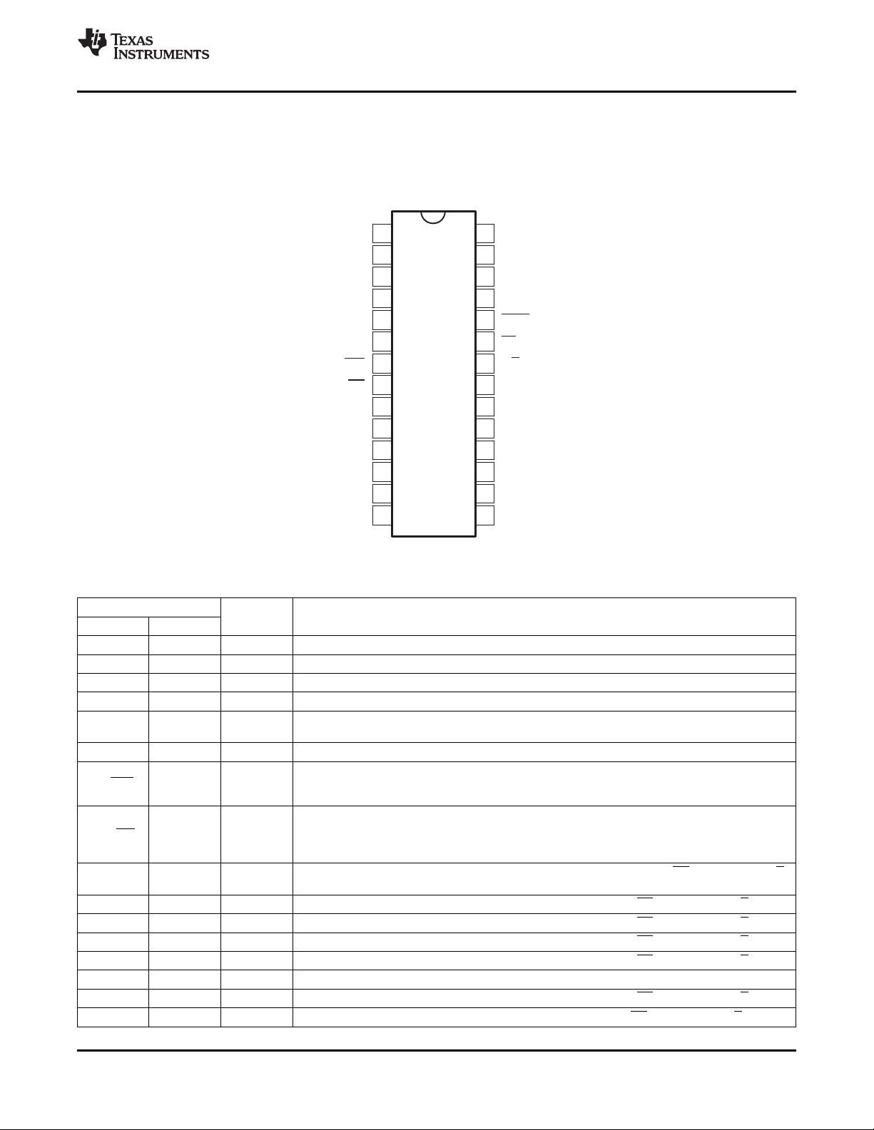
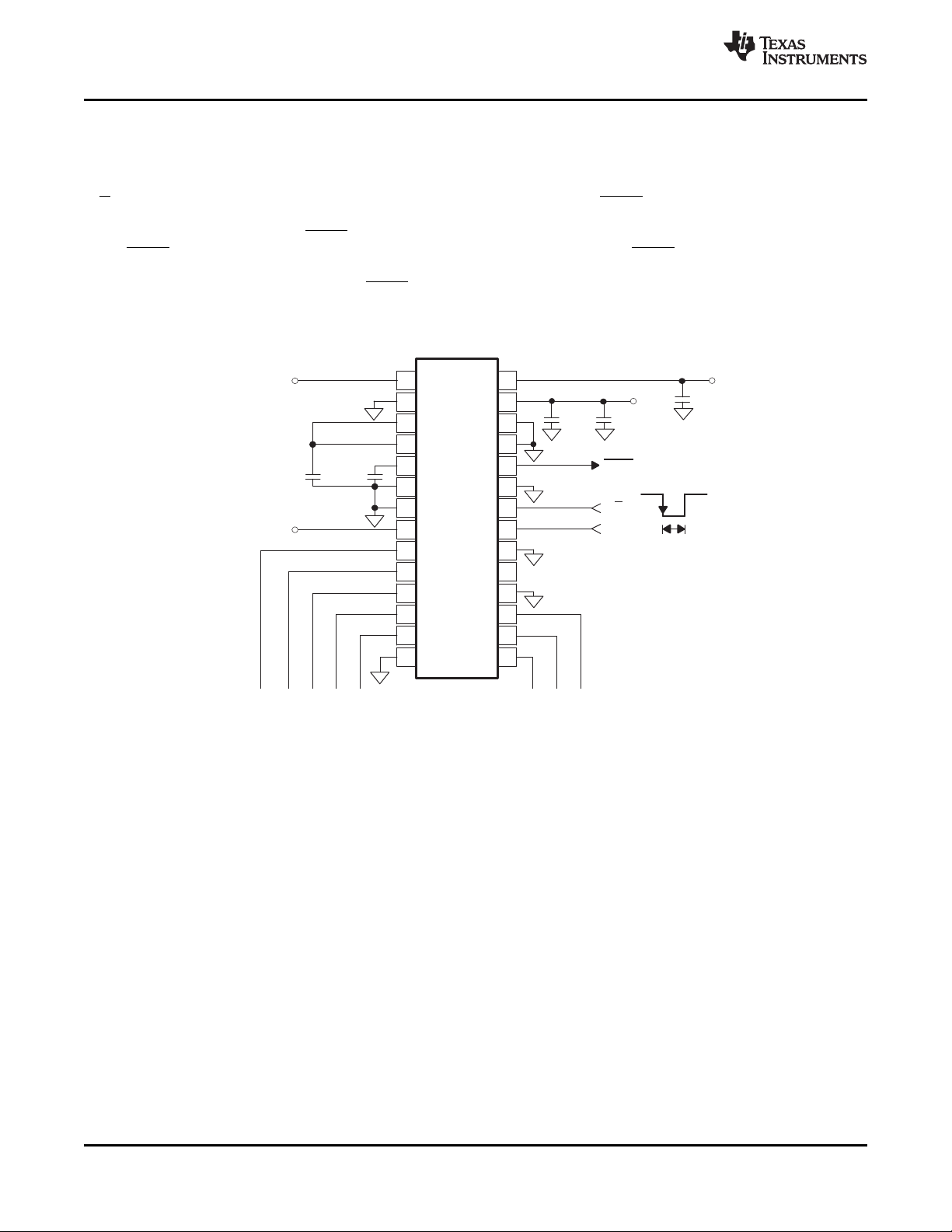
PIN CONFIGURATION
DW, PW PACKAGES
SO-28, TSSOP-28
(TOP VIEW)
(1)
(1) TSSOP-28 (PW) package available Q2, 2009.
Pin Assignments
PIN
NAME NO. I/O DESCRIPTION
R1
IN
1 Analog Input.
AGND1 2 Analog sense ground. Used internally as ground reference point. Minimal current flow
R2
IN
3 Analog Input.
CAP 4 Reference buffer output. 2.2- µ F tantalum capacitor to ground.
REF 5
AGND2 6 Analog ground
SB/ BTC 7 I high, data are output in a straight binary format. If low, data are output in a binary twos
EXT/ INT 8 I
D7 9 O
D6 10 O Data bit 6 if BYTE is high. Data bit 14 if BYTE is low. High-Z when CS is high and/or R/ C is low.
D5 11 O Data bit 5 if BYTE is high. Data bit 13 if BYTE is low. High-Z when CS is high and/or R/ C is low.
D4 12 O Data bit 4 if BYTE is high. Data bit 12 if BYTE is low. High-Z when CS is high and/or R/ C is low.
D3 13 O Data bit 3 if BYTE is high. Data bit 11 if BYTE is low. High-Z when CS is high and/or R/ C is low.
DGND 14 Digital ground
D2 15 O Data bit 2 if BYTE is high. Data bit 10 if BYTE is low. High-Z when CS is high and/or R/ C is low.
D1 16 O Data bit 1 if BYTE is high. Data bit 9 if BYTE is low. High-Z when CS is high and/or R/ C is low.
Copyright © 2008, Texas Instruments Incorporated Submit Documentation Feedback 5
DIGITAL
Reference input/output. Outputs internal 2.5-V reference. Can also be driven by external system
reference. In both cases, bypass to ground with a 2.2- µ F tantalum capacitor.
Output mode select. Selects straight binary or binary twos complement for output data format. If
complement format.
External/internal data select. Selects external/internal data clock for transmitting data. If high,
data is output synchronized to the clock input on DATACLK. If low, a convert command initiates
the transmission of the data from the previous conversion, along with 16-clock pulses output on
DATACLK.
Data bit 7 if BYTE is high. Data bit 15 (MSB) if BYTE is low. High-Z when CS is high and/or R/ C
is low. Leave unconnected when using serial output.
Product Folder Link(s): ADS8517
Page 6
ADS8517
SLAS527 – SEPTEMBER 2008 ..........................................................................................................................................................................................
Pin Assignments (continued)
D0 17 O
DATACLK 18 I/O synchronized to this clock. If EXT/ INT is low, DATACLK transmits 16 pulses after each
SDATA 19 O TAG as long as CS is low and R/ C is high. If EXT/ INT is low, data are valid on both the rising
TAG 20 I
BYTE 21 I
R/ C 22 I into the hold state and starts a conversion. With EXT/ INT is low, the transmission of the data
CS 23 I conversion. If EXT/ INT is low, this same falling edge will start the transmission of serial data
BUSY 24 O
PWRD 25 I
REFD 26 I
V
ANA
V
DIG
27 ADC core supply. Nominally +5 V. Decouple with 0.1- µ F ceramic and 10- µ F tantalum capacitors.
28 I/O supply. Nominally +1.8 V.
Data bit 0 (LSB) if BYTE is high. Data bit 8 if BYTE is low. High-Z when CS is high and/or R/ C is
low.
Data clock. Either an input or an output, depending on the EXT/ INT level. Output data are
conversion, and then remains low between conversions.
Serial data output. Data are synchronized to DATACLK, with the format determined by the level
of SB/ BTC. In the external clock mode, after 16 bits of data, the ADC outputs the level input on
and falling edges of DATACLK, and between conversions SDATA stays at the level of the TAG
input when the conversion was started.
Tag input for use in the external clock mode. If EXT is high, digital data input from TAG is output
on DATA with a delay that depends on the external clock mode.
Byte select. Selects the eight most significant bits (low) or eight least significant bits (high) on
parallel output pins.
Read/convert input. With CS low, a falling edge on R/ C puts the internal sample-and-hold circuit
results from the previous conversion is initiated.
Chip select. Internally ORed with R/ C. If R/ C is low, a falling edge on CS initiates a new
results from the previous conversion.
Busy output. At the start of a conversion, BUSY goes low and stays low until the conversion is
completed and the digital outputs have been updated.
Power-down input. If high, conversions are inhibited and power consumption is significantly
reduced. Results from the previous conversion are maintained in the output shift register.
Reference disable. REFD high shuts down the internal reference. The external reference is
required for conversions.
www.ti.com
6 Submit Documentation Feedback Copyright © 2008, Texas Instruments Incorporated
Product Folder Link(s): ADS8517
Page 7
10.0
9.5
9.0
8.5
8.0
Temperature( C)°
P
ower
-SupplyCurrent(mA)
-50 -25 0 25 50 75 100 125
2.520
2.515
2.510
2.505
2.500
2.495
2.490
2.485
2.480
Temperature( C)°
InternalReferenceV
oltage(V)
-50 -25 0 125100755025
10.0
9.5
9.0
8.5
8.0
SamplingFrequency(kHz)
Power
-SupplyCurrent(mA)
50 100 150 200
2
1
0
-1
-2
Temperature( C)°
Offset(mV)
-50 -25 1251007550250
Bipolar 10VRange±
0.10
0.05
0
Temperature(°C)
PositiveFull-ScaleError(%)
-40 -50 1251007550250
Bipolar10VRange
0
-0.05
-0.10
Temperature( C)°
NegativeFull-ScaleError(%)
-50 -45 1251007550250
Bipolar10VRange
ADS8517
www.ti.com
.......................................................................................................................................................................................... SLAS527 – SEPTEMBER 2008
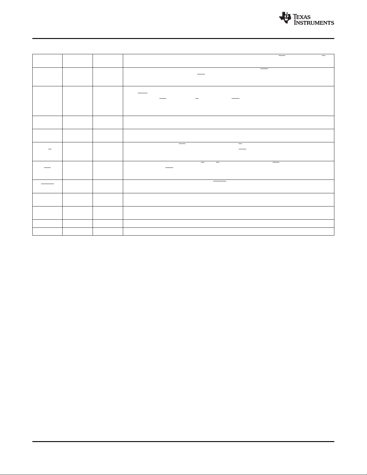
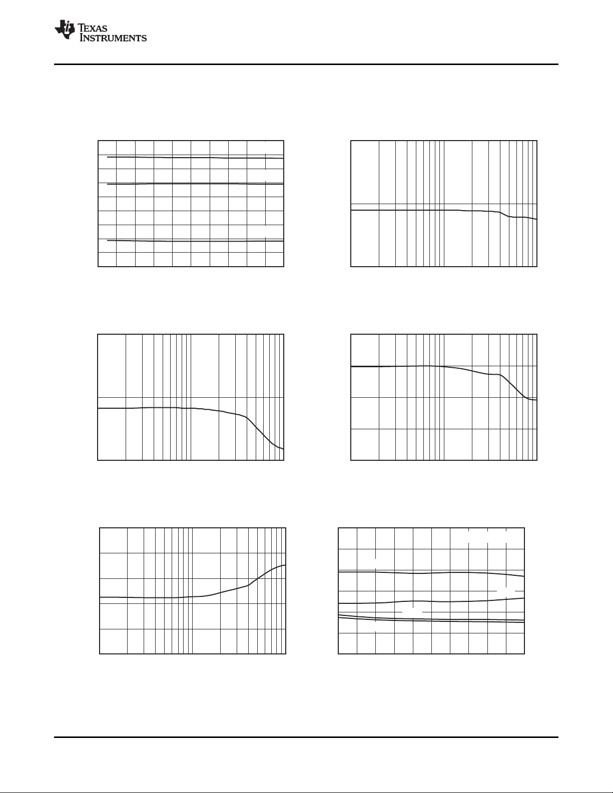
TYPICAL CHARACTERISTICS
At fS= 200 kHz, V
POWER-SUPPLY CURRENT INTERNAL REFERENCE VOLTAGE
vs FREE-AIR TEMPERATURE vs FREE-AIR TEMPERATURE
POWER-SUPPLY CURRENT BIPOLAR OFFSET ERROR
vs SAMPLING FREQUENCY vs FREE-AIR TEMPERATURE
= V
DIG
= 5 V, and using internal reference (see Figure 39 ), unless otherwise specified.
ANA
Figure 1. Figure 2.
Figure 3. Figure 4.
BIPOLAR POSITIVE FULL-SCALE ERROR BIPOLAR NEGATIVE FULL-SCALE ERROR
vs FREE-AIR TEMPERATURE vs FREE-AIR TEMPERATURE
Copyright © 2008, Texas Instruments Incorporated Submit Documentation Feedback 7
Figure 5. Figure 6.
Product Folder Link(s): ADS8517
Page 8
0.2
0.1
0
-0.1
-0.2
Temperature( C)°
Offset(mV)
-50 -25 1251007550250
Unipolar4VRange
0.2
0.1
0
-0.1
-0.2
Temperature( C)°
Offset(mV)
-50 -25 1251007550250
Unipolar5VRange
0.10
0.05
0
-0.05
-0.10
Temperature( C)°
Offset(mV)
-50 -25 1251007550250
Unipolar4VRange
0.10
0.05
0
-0.05
-0.10
Temperature( C)°
Offset(mV)
-50 -25 1251007550250
Unipolar5VRange
110
105
100
95
90
85
80
-80
-85
-90
-95
-100
-105
-110
Temperature( C)°
SFDR,SINAD,andSNR(dB)
THD(dB)
-50 -25 1251007550250
SINAD
SNR
SFDR
THD
f =10kHz,0dB
IN
89.5
89.0
88.5
88.0
87.5
Temperature( C)°
SINAD(dB)
-50 -25 1251007550250
f =100kHz
S
f =150kHz
S
f =10kHz,0dB
IN
f =200kHz
S
f =50kHz
S
ADS8517
SLAS527 – SEPTEMBER 2008 ..........................................................................................................................................................................................
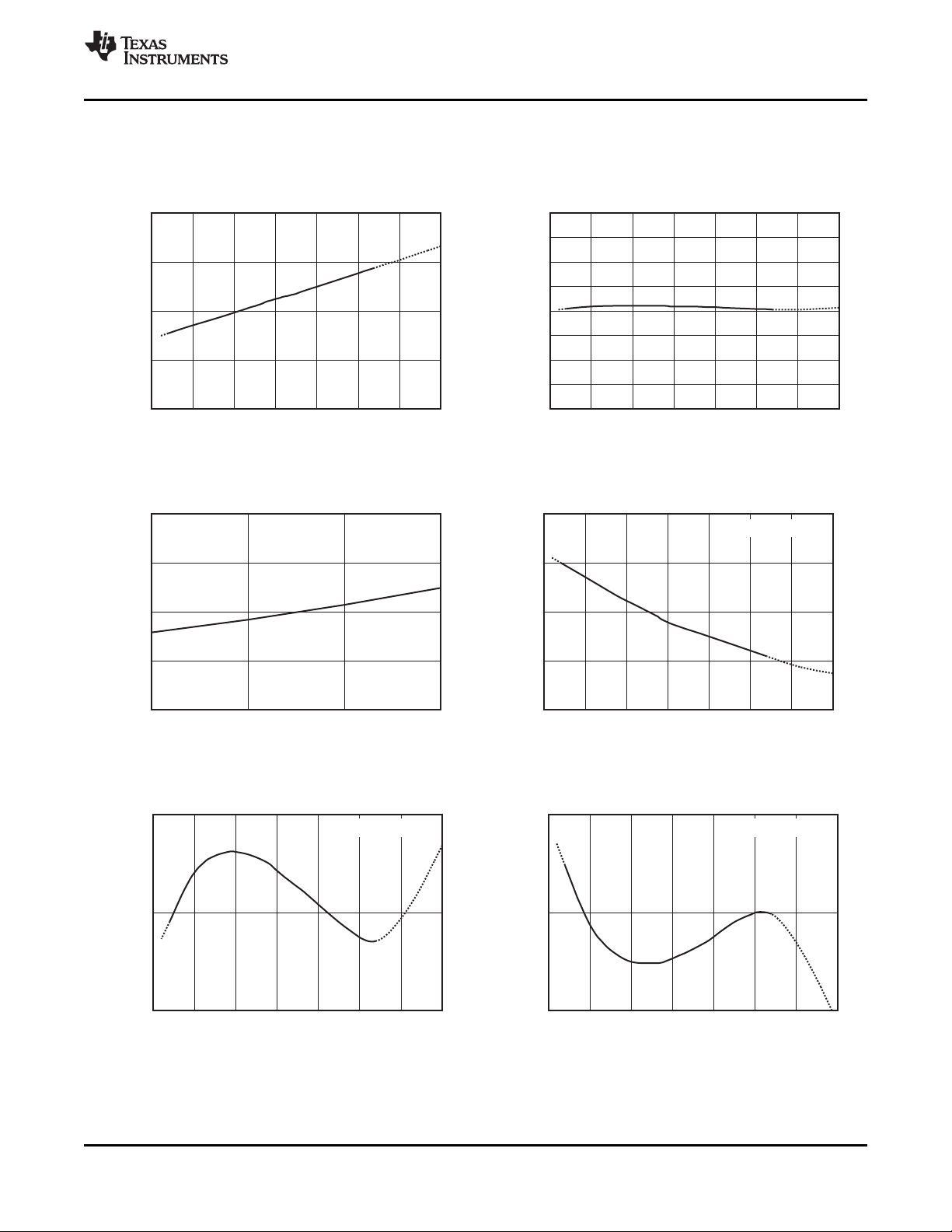
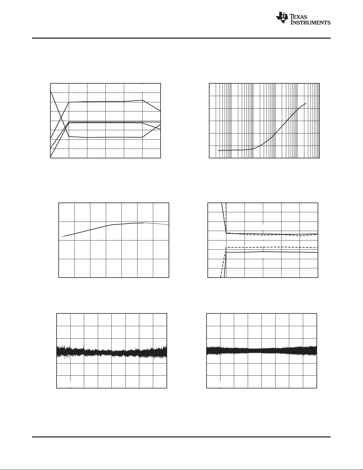
At fS= 200 kHz, V
TYPICAL CHARACTERISTICS (continued)
= V
DIG
UNIPOLAR OFFSET ERROR UNIPOLAR OFFSET ERROR
vs FREE-AIR TEMPERATURE vs FREE-AIR TEMPERATURE
UNIPOLAR FULL-SCALE ERROR UNIPOLAR FULL-SCALE ERROR
vs FREE-AIR TEMPERATURE vs FREE-AIR TEMPERATURE
= 5 V, and using internal reference (see Figure 39 ), unless otherwise specified.
ANA
Figure 7. Figure 8.
www.ti.com
8 Submit Documentation Feedback Copyright © 2008, Texas Instruments Incorporated
Figure 9. Figure 10.
AC PARAMETERS SIGNAL-TO-(NOISE+DISTORTION)
vs FREE-AIR TEMPERATURE vs FREE-AIR TEMPERATURE
Figure 11. Figure 12.
Product Folder Link(s): ADS8517
Page 9
100
90
80
70
60
50
40
30
20
10
InputSignalFrequency(kHz)
SINAD(dB)
0 2 4 8 106 12 14 16 18 20
-60dB
-20dB
0dB
100
90
80
InputSamplingFrequency(kHz)
SNR(dB)
1 10010
100
90
80
InputSamplingFrequency(kHz)
SINAD(dB)
1 10010
110
100
90
80
70
InputSamplingFrequency(kHz)
SFDR(dB)
1 10010
-70
-80
-90
-100
-110
-120
InputSamplingFrequency(kHz)
THD(dB)
1 10010
110
105
100
95
90
85
80
-80
-85
-90
-95
-100
-105
-110
ESR( )W
SFDR,SINAD,andSNR(dB)
THD(dB)
0 1 4 5 6 7 8 9 10
THD
SNR
SFDR
SINAD
f =10kHz,0dB
IN
32
ADS8517
www.ti.com
.......................................................................................................................................................................................... SLAS527 – SEPTEMBER 2008
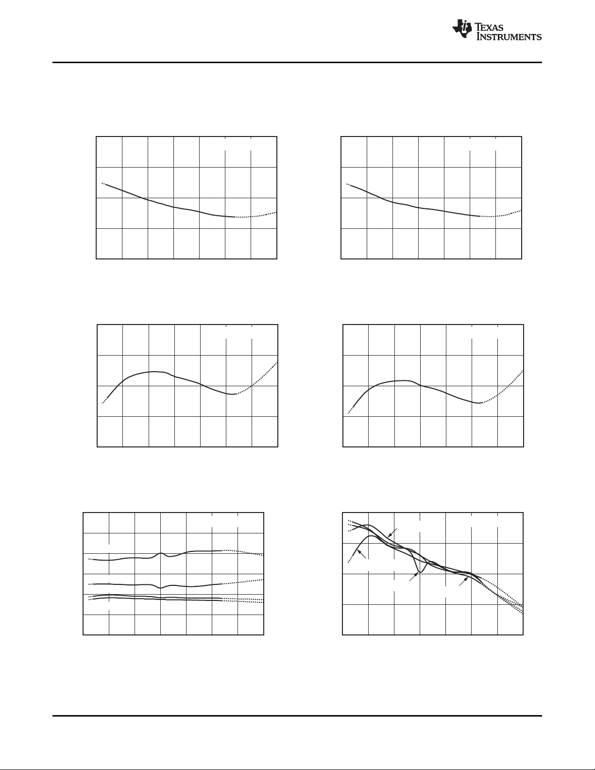
At fS= 200 kHz, V
vs INPUT FREQUENCY AND INPUT AMPLITUDE vs INPUT FREQUENCY
TYPICAL CHARACTERISTICS (continued)
= V
DIG
SIGNAL-TO-(NOISE+DISTORTION) SIGNAL-TO-NOISE RATIO
SIGNAL-TO-(NOISE+DISTORTION) SPURIOUS-FREE DYNAMIC RANGE
= 5 V, and using internal reference (see Figure 39 ), unless otherwise specified.
ANA
Figure 13. Figure 14.
vs INPUT FREQUENCY vs INPUT FREQUENCY
TOTAL HARMONIC DISTORTION AC PARAMETERS
vs INPUT FREQUENCY vs CAP PIN CAPACITOR ESR
Copyright © 2008, Texas Instruments Incorporated Submit Documentation Feedback 9
Figure 15. Figure 16.
Figure 17. Figure 18.
Product Folder Link(s): ADS8517
Page 10
110
105
100
95
90
85
80
75
70
-70
-75
-80
-85
-90
-95
-100
-105
-110
Power-SupplyVoltage(V)
SFDR,SINAD,andSNR(dB)
THD(dB)
4.00 4.25 4.50 4.75 5.00 5.25 5.50
THD
SNR
SFDR
SINAD
f =10kHz,0dB
IN
-20
-30
-40
-50
-60
-70
-80
Power-SupplyRippleFrequency(Hz)
OutputRejection(dB)
10 1M100 1k 10k 100k
2.40
2.35
2.30
2.25
2.20
Temperature( C)°
ConversionTime( s)m
-50 -25 1251007550250
2.0
1.5
1.0
0.5
0
-0.5
-1.0
-1.5
-2.0
Power-SupplyVoltage(V)
INL/DNLMaxandMin(LSB)
4.00 4.25 4.50 4.75 5.00 5.25 5.50
INLMax
INLMin
DNLMin
DNLMax
3
2
1
0
-1
-2
-3
Code
INL(LSB)
0 8192 16384 24576 32768 40960 49152 57344 65535
AllCodesINL
3
2
1
0
-1
-2
-3
Code
DNL(LSB)
0 8192 16384 24576 32768 40960 49152 57344 65535
AllCodesDNL
ADS8517
SLAS527 – SEPTEMBER 2008 ..........................................................................................................................................................................................
At fS= 200 kHz, V
TYPICAL CHARACTERISTICS (continued)
= V
DIG
vs POWER-SUPPLY VOLTAGE vs POWER-SUPPLY RIPPLE FREQUENCY
vs FREE-AIR TEMPERATURE vs POWER-SUPPLY VOLTAGE
= 5 V, and using internal reference (see Figure 39 ), unless otherwise specified.
ANA
AC PARAMETERS OUTPUT REJECTION
Figure 19. Figure 20.
INTEGRAL LINEARITY ERROR AND
CONVERSION TIME DIFFERENTIAL LINEARITY ERROR
www.ti.com
Figure 21. Figure 22.
INTEGRAL LINEARITY ERROR DIFFERENTIAL LINEARITY ERROR
10 Submit Documentation Feedback Copyright © 2008, Texas Instruments Incorporated
Figure 23. Figure 24.
Product Folder Link(s): ADS8517
Page 11
0
-10
-20
-30
-40
-50
-60
-70
-80
-90
-100
-110
-120
-130
Frequency(kHz)
Amplitude(dB)
0 25 50 10075
4096PointFFT
f =1kHz,0dB
IN
Frequency(kHz)
0 25 50 10075
4096PointFFT
f =10kHz,0dB
IN
0
-10
-20
-30
-40
-50
-60
-70
-80
-90
-100
-110
-120
-130
Amplitude(dB)
Frequency(kHz)
0 25 50 10075
4096PointFFT
f =20kHz,0dB
IN
0
-10
-20
-30
-40
-50
-60
-70
-80
-90
-100
-110
-120
-130
Amplitude(dB)
ADS8517
www.ti.com
.......................................................................................................................................................................................... SLAS527 – SEPTEMBER 2008
At fS= 200 kHz, V
TYPICAL CHARACTERISTICS (continued)
= V
DIG
= 5 V, and using internal reference (see Figure 39 ), unless otherwise specified.
ANA
FFT FFT
Figure 25. Figure 26.
FFT
Copyright © 2008, Texas Instruments Incorporated Submit Documentation Feedback 11
Figure 27.
Product Folder Link(s): ADS8517
Page 12
1
2
3
4
5
6
7
8
9
10
11
12
13
14
28
27
26
25
24
23
22
21
20
19
18
17
16
15
ADS8517
+5 V
+
+
ConvertPulse
40nsmin
0.1 mF 10 mF
+
NOTE:(1)NC=notconnected.
B11B12B13B1 4B15
(MSB)
Pin21
LOW
B3B4B5B6B7Pin21
HIGH
NC
(1)
B8B9B10
B0
(LSB)
B1B2
BUSY
R/C
BYTE
±10 V
2.2 Fm
+5V
2.2 Fm
+1.8V
0.1 Fm
ADS8517
SLAS527 – SEPTEMBER 2008 ..........................................................................................................................................................................................
www.ti.com
BASIC OPERATION
PARALLEL OUTPUT
Figure 28 shows a basic circuit for operating the ADS8517 with a ± 10-V input range and parallel output. Taking
R/ C (pin 22) low for a minimum of 40 ns (5 µ s max) initiates a conversion. BUSY (pin 24) goes low and stays low
until the conversion completes and the output register updates. If BYTE (pin 21) is low, the eight most significant
bits (MSBs) will be valid when BUSY rises; if BYTE is high, the eight least significant bits (LSBs) will be valid
when BUSY rises. Data are output in binary twos complement (BTC) format. BUSY going high can be used to
latch the data. After the first byte has been read, BYTE can be toggled, allowing the remaining byte to be read.
All convert commands are ignored while BUSY is low.
The ADS8517 begins tracking the input signal at the end of the conversion. Allowing 5 µ s between convert
commands assures accurate acquisition of a new signal.
Figure 28. Basic ± 10-V Operation, Both Parallel and Serial Output
12 Submit Documentation Feedback Copyright © 2008, Texas Instruments Incorporated
Product Folder Link(s): ADS8517
Page 13
1
2
3
4
5
6
7
8
9
10
11
12
13
14
28
27
26
25
24
23
22
21
20
19
18
17
16
15
ADS8517
+5 V
+
+
ConvertPulse
40nsmin
0.1 mF 10 mF
+
NC
(1)
BUSY
R/C
SDATA
±10 V
+
NC
(1)
NC
(1)
NC
(1)
NC
(1)
NC
(1)
NC
(1)
NC
(1)
DATACLK
NOTE:(1)NC=notconnected.
2.2 Fm22 Fm
+1.8V
0.1 Fm
ADS8517
www.ti.com
.......................................................................................................................................................................................... SLAS527 – SEPTEMBER 2008
SERIAL OUTPUT
Figure 29 shows a basic circuit to operate the ADS8517 with a ± 10-V input range and serial output. Taking R/ C
(pin 22) low for 40 ns (5 µ s max) initiates a conversion and outputs valid data from the previous conversion on
SDATA (pin 19) synchronized to 16 clock pulses output on DATACLK (pin 18). BUSY (pin 24) goes low and
stays low until the conversion completes and the serial data have been transmitted. Data are output in BTC
format, MSB first, and are valid on both the rising and falling edges of the data clock. BUSY going high can be
used to latch the data. All convert commands are ignored while BUSY is low.
The ADS8517 begins tracking the input signal at the end of the conversion. Allowing 5 µ s between convert
commands assures accurate acquisition of a new signal.
Figure 29. Basic ± 10-V Operation with Serial Output
Copyright © 2008, Texas Instruments Incorporated Submit Documentation Feedback 13
Product Folder Link(s): ADS8517
Page 14

ADS8517
SLAS527 – SEPTEMBER 2008 ..........................................................................................................................................................................................
www.ti.com
STARTING A CONVERSION
The combination of CS (pin 23) and R/ C (pin 22) held low for a minimum of 40 ns puts the sample-and-hold of
the ADS8517 in the hold state and starts conversion N. BUSY (pin 24) goes low and stays low until conversion N
completes and the internal output register has been updated. All new convert commands received while BUSY is
low are ignored.
The ADS8517 begins tracking the input signal at the end of the conversion. Allowing 5 µ s between convert
commands assures accurate acquisition of a new signal. Refer to Table 2 and Table 3 for a summary of CS,
R/ C, and BUSY states, and Figure 30 through Figure 36 for timing diagrams.
Table 2. Control Functions When Using Parallel Output (DATACLK Tied Low, EXT/ INT Tied High)
CS R/ C BUSY OPERATION
1 X X None. Data bus is in High-Z state.
↓ 0 1 Initiates conversion N. Data bus remains in High-Z state.
0 ↓ 1 Initiates conversion N. Data bus enters High-Z state.
0 1 ↑ Conversion N completed. Valid data from conversion N on the data bus.
↓ 1 1 Enables data bus with valid data from conversion N.
↓ 1 0 Enables data bus with valid data from conversion N – 1
0 ↑ 0 Enables data bus with valid data from conversion N – 1
0 0 ↑ New conversion initiated without acquisition of a new signal. Data are invalid. CS and/or R/ C
X X 0 New convert commands ignored. Conversion N in progress.
(1) See Figure 30 and Figure 31 for constraints on data valid from conversion N – 1.
must be high when BUSY goes high.
CS and R/ C are internally ORed and level-triggered. It does not matter which input goes low first when initiating a
conversion. If, however, it is critical that CS or R/ C initiates conversion N, be sure the less critical input is low at
least t
≥ 10 ns before the initiating input. If EXT/ INT (pin 8) is low when initiating conversion N, serial data from
su2
conversion N – 1 is output on SDATA (pin 19) following the start of conversion N. See Internal Data Clock in the
Reading Data section for more information.
To reduce the number of control pins, CS can be tied low using R/ C to control the read and convert modes. This
configuration has no effect when using the internal data clock in the serial output mode. However, when using an
active external data clock, the parallel and serial outputs are affected whenever R/ C goes high; refer to the
Reading Data section for more information. In the internal clock mode, data are clocked out every convert cycle
regardless of the states of CS and R/ C. The conversion result is available as soon as BUSY returns to high.
Therefore, data always represent the previously-completed conversion, even when read during a conversion.
(1)
. Conversion N in progress.
(1)
. Conversion N in progress.
14 Submit Documentation Feedback Copyright © 2008, Texas Instruments Incorporated
Product Folder Link(s): ADS8517
Page 15

ADS8517
www.ti.com
.......................................................................................................................................................................................... SLAS527 – SEPTEMBER 2008
READING DATA
The ADS8517 outputs serial or parallel data in straight binary (SB) or binary twos complement data output
format. If SB/ BTC (pin 7) is high, the output is in SB format; if it is low, the output is in BTC format. Refer to
Table 4 for the ideal output codes. The first conversion immediately following a power-up does not produce a
valid conversion result.
The parallel output can be read without affecting the internal output registers; however, reading the data through
the serial port shifts the internal output registers one bit per data clock pulse. As a result, data can be read on the
parallel port before reading the same data on the serial port, but data cannot be read through the serial port
before reading the same data on the parallel port.
Table 3. Control Functions When Using Serial Output
CS R/ C BUSY EXT/ INT DATACLK OPERATION
↓ 0 1 0 Output Initiates conversion N. Valid data from conversion N – 1 clocked out on SDATA.
0 ↓ 1 0 Output Initiates conversion N. Valid data from conversion N – 1 clocked out on SDATA.
↓ 0 1 1 Input Initiates conversion N. Internal clock still runs conversion process.
0 ↓ 1 1 Initiates conversion N. Internal clock still runs conversion process.
↓ 1 1 1 Input Conversion N completed. Valid data from conversion N clocked out on SDATA
synchronized to external data clock.
↓ 1 0 1 Input Valid data from conversion N – 1 output on SDATA synchronized to external data clock.
Conversion N in progress.
0 ↑ 0 1 Input Valid data from conversion N – 1 output on SDATA synchronized to external data clock.
Conversion N in progress.
0 0 ↑ X Input New conversion initiated without acquisition of a new signal. Data are invalid. CS and/or
R/ C must be high when BUSY goes high.
X X 0 X X New convert commands ignored. Conversion N in progress..
(1) See Figure 34 , Figure 35 , and Figure 36 for constraints on data valid from conversion N – 1.
(1)
Table 4. Output Codes and Ideal Input Voltages
DIGITAL OUTPUT
BINARY TWOS COMPLEMENT
DESCRIPTION ANALOG INPUT
Full-scale range ± 10 0 V to 5 V 0 V to 4 V
Least significant bit (LSB) 305 µ V 76 µ V 61 µ V BINARY CODE CODE BINARY CODE HEX CODE
+Full-scale (FS – 1LSB) 9.999695 V 4.999924 V 3.999939 V 0111 1111 1111 1111 7FFF 1111 1111 1111 1111 FFFF
Midscale 0 V 2.5 V 2 V 0000 0000 0000 0000 0000 1000 0000 0000 0000 8000
1 LSB below midscale 305 µ V 2.499924 V 1.999939 V 1111 1111 1111 1111 FFFF 0111 1111 1111 1111 7FFF
– Full-scale -10 V 0 V 0 V 1000 0000 0000 0000 8000 0000 0000 0000 0000 0000
(SB/ BTC LOW) STRAIGHT BINARY (SB/ BTC HIGH)
HEX
Parallel Output
To use the parallel output, tie EXT/ INT (pin 8) high and DATACLK (pin 18) low. SDATA (pin 19) should be left
unconnected. The parallel output is active when R/ C (pin 22) is high and CS (pin 23) is low. Any other
combination of CS and R/ C 3-states the parallel output. Valid conversion data can be read in two 8-bit bytes on
D7-D0 (pins 9-13 and 15-17). When BYTE (pin 21) is low, the eight most significant bits are valid with the MSB
on D7. When BYTE is high, the eight least significant bits are valid with the LSB on D0. BYTE can be toggled to
read both bytes within one conversion cycle.
Upon initial device power-up, the parallel output contains indeterminate data.
Copyright © 2008, Texas Instruments Incorporated Submit Documentation Feedback 15
Product Folder Link(s): ADS8517
Page 16

R/C
BUSY
MODE
Parallel
Data Bus
BYTE
t
1
t
3
t
4
t
1
t
3
t
6
t
7
t
5
t
6
t
8
t
12
t
11
t
10
t
12
t
2
t
9
t
12
t
12
t
12
t
9
t
12
Previous
High Byte Valid
Hi-Z
Previous High
Byte Valid
Previous Low
Byte Valid
Not Valid
High Byte
Valid
Low Byte
Valid
Hi-Z
High Byte
Valid
Acquire Convert Acquire Convert
t
21
t
21
t
21
t
21
t
21
t
21
t
21
t
21
t
21
t
21
t
21
t
9
t
21
t
9
Hi-Z State High Byte Hi-Z State Low Byte Hi-Z State
t
4
t
3
t
1
R/C
BUSY
CS
Data Bus
BYTE
ADS8517
SLAS527 – SEPTEMBER 2008 ..........................................................................................................................................................................................
www.ti.com
Parallel Output (After a Conversion)
After conversion N is completed and the output registers have been updated, BUSY (pin 24) goes high. Valid
data from conversion N are available on D7-D0 (pin 9-13 and 15-17). BUSY going high can be used to latch the
data. Refer to Table 5 , Figure 30 , and Figure 31 for timing specifications.
Figure 30. Conversion Timing With Parallel Output ( CS and DATACLK Tied Low, EXT/INT Tied High)
16 Submit Documentation Feedback Copyright © 2008, Texas Instruments Incorporated
Figure 31. CS to Control Conversion and Read Timing With Parallel Outputs
Product Folder Link(s): ADS8517
Page 17
ADS8517
www.ti.com
.......................................................................................................................................................................................... SLAS527 – SEPTEMBER 2008
Parallel Output (During a Conversion)
After conversion N has been initiated, valid data from conversion N – 1 can be read and are valid up to 2.2 µ s
after the start of conversion N. Do not attempt to read data beyond 2.2 µ s after the start of conversion N until
BUSY (pin 24) goes high; doing so may result in reading invalid data. Refer to Table 5 , Figure 30 , and Figure 31
for timing constraints.
Table 5. Conversion and Data Timing with Parallel Interface at T
SYMBOL DESCRIPTION MIN TYP MAX UNITS
t
Convert pulse width 0.04 5 µ s
1
t
Data valid delay after R/ C low 2.3 2.5 µ s
2
t
BUSY delay from start of conversion 20 85 ns
3
t
BUSY low 2.3 2.5 µ s
4
t
BUSY delay after end of conversion 90 ns
5
t
Aperture delay 40 ns
6
t
Conversion time 1.8 2.2 µ s
7
t
Acquisition time 2.7 µ s
8
t
Bus relinquish time 10 83 ns
9
t
BUSY delay after data valid 20 60 ns
10
t
Previous data valid after start of conversion 1.8 2.2 µ s
11
t
R/ C to CS setup time 10 ns
21
t7+ t
Throughput time 5 µ s
8
= – 40 ° C to +85 ° C
A
Serial Output
Data can be clocked out with the internal data clock or an external data clock. When using the serial output, be
careful with the parallel outputs, D7-D0 (pins 9-13 and 15-17), because these pins come out of a High-Z state
whenever CS (pin 23) is low and R/ C (pin 22) is high. The serial output cannot be 3-stated and is always active.
Refer to the Applications Information section for specific serial interfaces. If an external clock is used, the TAG
input can be used to daisy-chain multiple ADS8517 data pins together.
Internal Data Clock (During a Conversion)
To use the internal data clock, tie EXT/ INT (pin 8) low. The combination of R/ C (pin 22) and CS (pin 23) low
initiates conversion N and activates the internal data clock (typically, a 900-kHz clock rate). The ADS8517
outputs 16 bits of valid data, MSB first, from conversion N – 1 on SDATA (pin 19), synchronized to 16 clock pulses
output on DATACLK (pin 18). The data are valid on both the rising and falling edges of the internal data clock.
The rising edge of BUSY (pin 24) can be used to latch the data. After the 16th clock pulse, DATACLK remains
low until the next conversion is initiated, while SDATA returns to the state of the TAG pin input sensed at the
start of transmission. Refer to Table 6 and Figure 33 for more information.
Copyright © 2008, Texas Instruments Incorporated Submit Documentation Feedback 17
Product Folder Link(s): ADS8517
Page 18

ADS8517
SLAS527 – SEPTEMBER 2008 ..........................................................................................................................................................................................
www.ti.com
External Data Clock
To use an external data clock, tie EXT/ INT (pin 8) high. The external data clock is not and cannot be
synchronized with the internal conversion clock; care must be taken to avoid corrupting the data. To enable the
output mode of the ADS8517, CS (pin 23) must be low and R/ C (pin 22) must be high. DATACLK must be high
for 20% to 70% of the total data clock period; the clock rate can be between dc and 10 MHz. Serial data from
conversion N can be output on SDATA (pin 19) after conversion N completes or during conversion N+1.
An obvious way to simplify control of the converter is to tie CS low and use R/ C to initiate conversions.
While this configuration is perfectly acceptable, there is a possible problem when using an external data clock. At
an indeterminate point from 12 µ s after the start of conversion N until BUSY rises, the internal logic shifts the
results of conversion N into the output register. If CS is low, R/ C high, and the external clock is high at this point,
data are lost. Consequently, with CS low, either R/ C and/or DATACLK must be low during this period to avoid
losing valid data.
External Data Clock (After a Conversion)
After conversion N is completed and the output registers have been updated, BUSY (pin 24) goes high. With CS
low and R/ C high, valid data from conversion N are output on SDATA (pin 19) synchronized to the external data
clock input on DATACLK (pin 18). The MSB is valid on the first falling edge and the second rising edge of the
external data clock. The LSB is valid on the 16th falling edge and 17th rising edge of the data clock. TAG (pin
20) inputs a bit of data for every external clock pulse. The first bit input on TAG is valid on SDATA on the 17th
falling edge and the 18th rising edge of DATACLK; the second input bit is valid on the 18th falling edge and the
19th rising edge, etc. With a continuous data clock, TAG data is output on SDATA until the internal output
registers are updated with the results from the next conversion. Refer to Table 6 and Figure 35 for more
information.
External Data Clock (During a Conversion)
After conversion N has been initiated, valid data from conversion N – 1 can be read and are valid up to 2.2 µ s
after the start of conversion N. Do not attempt to clock out data from 2.2 µ s after the start of conversion N until
BUSY (pin 24) rises; doing so results in data loss.
NOTE:
For the best possible performance when using an external data clock, data should not
be clocked out during a conversion.
The switching noise of the asynchronous data clock can cause digital feedthrough, degrading converter
performance. Refer to Table 6 and Figure 36 for more information.
18 Submit Documentation Feedback Copyright © 2008, Texas Instruments Incorporated
Product Folder Link(s): ADS8517
Page 19

1 2
t
su1
t
su1
CS
R/C
External
DATACLK
CS Set Low, Discontinuous Ext DATACLK
t
su1
t
su1
R/C
CS
External
DATACLK
R/C Set Low, Discontinuous Ext DATACLK
t
su2
t
su2
CS
R/C
t
su3
BUSY
External
DATACLK
CS Set Low, Discontinuous Ext DATACLK
t
d9
ADS8517
www.ti.com
.......................................................................................................................................................................................... SLAS527 – SEPTEMBER 2008
Table 6. Timing Requirements (T
= – 40 ° C to +85 ° C)
A
PARAMETER MIN TYP MAX UNIT
t
t
t
t
t
t
conv
t
acq
t
conv
t
t
t
t
t
t
t
t
su1
t
su2
t
t
t
d10
t
su3
t
d11
t
su4
t
Pulse duration, convert 0.04 5 µ s
w1
Delay time, BUSY from R/ C low 20 85 ns
d1
Pulse duration, BUSY low 2.3 2.5 µ s
w2
Delay time, BUSY, after end of conversion 90 ns
d2
Delay time, aperture 40 ns
d3
Conversion time 2.0 2.2 2.4 µ s
Acquisition time 2.6 2.7 µ s
+ t
Cycle time 5 µ s
acq
Delay time, R/ C low to internal DATACLK output 171 ns
d4
Cycle time, internal DATACLK 92 96 98 ns
c1
Delay time, data valid to internal DATACLK high 2 3.5 ns
d5
Delay time, data valid after internal DATACLK low 41 43 ns
d6
Cycle time, external DATACLK 35 ns
c2
Pulse duration, external DATACLK high 15 ns
w3
Pulse duration, external DATACLK low 15 ns
w4
Setup time, R/ C rise/fall to external DATACLK high 15 ns
Setup time, R/ C transition to CS transition 10 ns
Delay time, data valid from external DATCLK high 2 25 40 ns
d8
Delay time, CS rising edge to external DATACLK rising edge 15 ns
d9
Delay time, previous data available after CS, R/ C low 1.8 2.2 µ s
Setup time, BUSY transition to first external DATACLK 5 ns
Delay time, final external DATACLK to BUSY rising edge 825 ns
Setup time, TAG valid before rising edge of DATACLK 2 ns
Hold time, TAG valid after rising edge of DATACLK 2 ns
h1
Copyright © 2008, Texas Instruments Incorporated Submit Documentation Feedback 19
Figure 32. Critical Timing Parameters
Product Folder Link(s): ADS8517
Page 20
R/C
BUSY
STATUS
(N+1)th Accquisition
(N+1)th Conversion
Error
Correction
Nth Conversion
Error
Correction
Internal
DATACLK
(N−1)th Conversion Data
SDATA
Nth Conversion Data
(N+2)th Accquisition
1 2 16216
D15 D0 D15 D0
TAG = 0 TAG = 0
TAG = 0
8 starts READ
CS
, EXT/INT, and TAG are tied low
t
w1
t
d1
t
w2
t
d3
t
d11
t
d2
t
d3
t
w1
t
d1
t
w2
t
d11
t
d2
t
conv
t
acq
t
conv
t
acq
t
d4
t
d4
t
c1
t
d5
t
d6
1
(N + 1)th (N + 2)th
BUSY
STATUS
(N+1)th Accquisition (N+1)th Conversion
Error
Correction
Nth Conversion
Error
Correction
External
DATACLK
SDATA
Nth Data (N+1)th Data
(N+2)th Accquisition
TAG = 0
No more
data to
shift out
No more
data to
shift out
TAG = 0
TAG = 0
TAG = 0
TAG = 0
R/C
EXT/INT tied high, CS and TAG are tied low
tw1 + t
su1
starts READ
t
w1
t
w1
t
d1
t
w2
t
d1
t
w2
t
d3
t
d11
t
d2
t
d3
t
d11
t
d2
t
su1
t
conv
t
acq
t
conv
t
acq
t
su3
t
su1
t
su3
1
16
1
2 16
1 16
1
2
16
(N + 1)th (N + 2)th
ADS8517
SLAS527 – SEPTEMBER 2008 ..........................................................................................................................................................................................
Figure 33. Basic Conversion Timing: Internal DATACLK (Read Previous Data During Conversion)
www.ti.com
20 Submit Documentation Feedback Copyright © 2008, Texas Instruments Incorporated
Figure 34. Basic Conversion Timing: External DATACLK
Product Folder Link(s): ADS8517
Page 21

BUSY
STATUS
(N+1) th Accquisition
Error
Correction
Nth Conversion
External
DATACLK
DATA
Nth Conversion Data
SYNC= 0
D15
0
1
2
3
1514 16
TAG
T01
D05
D10D12D13
D14
T00 T04
T03T02
T13T12T11
T06
T16
T15
T14
Ty y
54
11 12 1310
D11
T05
D04 D03 D02 D01
Txx
D00
T00
T17
R/C
EXT/INT tied high, CS tied low
tw1+ t
su1
starts READ
t
w1
t
d1
t
w2
t
su1
t
d3
t
d11
t
d2
t
conv
t
acq
t
d3
t
d1
t
su3
t
w3
t
c2
t
w4
t
su1
t
d8
t
d8
t
su4
t
h1
BUSY
STATUS
Error
Correction
(N + 1)th Conversion
External
DATACLK
SDATA
Nth Conversion Data
D15
0
1 2 3 1514 16
D05D10D12D13D14
54 11 12 1310
D11 D00D04 D03 D02 D01
R/C
EXT/INT tied high, CS and TAG tied low
Rising DATACLK change DATA, tw1 + t
su1
Starts READ
TAG is not recommended for this mode. There is not enough
time to do so without violating t
d11
.
t
w1
t
d1
t
w2
t
d10
t
d3
t
su3
t
conv
t
d2
t
su1
t
w3
t
c2
t
w4
t
d11
t
d8
t
d8
ADS8517
www.ti.com
.......................................................................................................................................................................................... SLAS527 – SEPTEMBER 2008
Figure 35. Read After Conversion (Discontinuous External DATACLK)
Copyright © 2008, Texas Instruments Incorporated Submit Documentation Feedback 21
Figure 36. Read During Conversion (Discontinuous External DATACLK)
Product Folder Link(s): ADS8517
Page 22

2 3332 3416154 19 20 21181
A00
D Q D Q
D Q D Q
B00
A15
B15
TAG(B)
DATA(A)
DATA(B)
DATACLK
Nth Conversion Data
B15 B14 B13
A15B00
B01
A00
A14 A13 A12
A15 A14 A13 A00A01
17
ADS8517A ADS8517B
TAG TAG
DATA DATA
DATACLK DATACLK
Processor
SCLK
GPIO
GPIO
SDI
TAG(A)=0
TAG(A)=0
R/C
(bothAandB)
BUSY
(bothAandB)
SYNC
(bothAandB)
External
DATACLK
DATA(B)
DATA(A)
CS
R/C
R/C
CS
EXT/INT tied high, CS of both converter A and B, TAG input of converter A are tied low.
3
ADS8517
SLAS527 – SEPTEMBER 2008 ..........................................................................................................................................................................................
www.ti.com
TAG FEATURE
The TAG feature allows data from multiple ADS8517 converters to be read on a single serial line. The converters
are cascaded together using the DATA pins as outputs and the TAG pins as inputs, as illustrated in Figure 37 .
The DATA pin of the last converter drives the processor serial data input. Data are then shifted through each
converter, synchronous to the externally supplied data clock, onto the serial data line. The internal clock cannot
be used for this configuration.
The preferred timing uses the discontinuous, external data clock during the sampling period. Data must be read
during the sampling period because there is not sufficient time to read data from multiple converters during a
conversion period without violating the t
must be sufficiently long enough to allow all data words to be read before starting a new conversion.
Note that in Figure 37 , the state of the DATA pin at the end of a READ cycle reflects the state of the TAG pin at
the start of the cycle for each converter. The ADS8517 works the same way when it is running in external or
internal clock mode. That is, the state of the TAG pin is shown on the DATA pin at the 17th clock after all 16 bits
have shifted out. However, it is only practical to use the TAG feature with the external clock mode when multiple
ADS8517s are daisy-chained, so that they are running at the same clock speed. For example, when two
converters (ADS8517A and ADS8517B) are cascaded together, the 17th external clock cycle brings the MSB
data of ADS8517A onto the DATA pin of ADS8517B.
constraint (see the External Data Clock section). The sampling period
d11
22 Submit Documentation Feedback Copyright © 2008, Texas Instruments Incorporated
Figure 37. Timing of TAG Feature With Single Conversion (Using External DATACLK)
Product Folder Link(s): ADS8517
Page 23

1
2
3
4
5
AGND2
CAP
REF
AGND1
+
2.2 Fm
2.2 Fm
2.2 Fm
2.2 Fm
V
IN
V
IN
V
IN
R1
IN
R2
IN
6
50kW 50kW
1MW 1MW
+5V
+5V
+
1
2
3
4
5
AGND2
CAP
REF
AGND1
+
6
R1
IN
R2
IN
+
2.2 Fm
2.2 Fm
50kW
1MW
+5V
4
5
+
6
+
1
2
3
AGND2
CAP
REF
AGND1
R1
IN
R2
IN
±10V 0Vto5V 0Vto4V
1
2
3
4
5
AGND2
CAP
REF
AGND1
+
2.2 Fm
2.2 Fm
2.2 Fm
2.2 Fm
V
IN
V
IN
V
IN
R1
IN
R2
IN
6
1MW
+
1
2
3
4
5
AGND2
CAP
REF
AGND1
+
6
R1
IN
R2
IN
+
2.2 Fm
2.2 Fm
4
5
+
6
+
1
2
3
AGND2
CAP
REF
AGND1
R1
IN
R2
IN
±10V 0Vto5V 0Vto4V
ADS8517
www.ti.com
.......................................................................................................................................................................................... SLAS527 – SEPTEMBER 2008
ANALOG INPUTS
The ADS8517 offers three analog input ranges, as shown in Table 1 . The offset specification is factory-calibrated
with internal resistors. The gain specification is factory-calibrated with 0.1%, 0.25-W external resistors, as shown
in Figure 38 and Figure 39 . The external resistors can be omitted if a larger gain error is acceptable or if using
software calibration. The hardware trim circuitry shown in Figure 38 and Figure 39 can reduce the error to zero.
Figure 38. Circuit Diagrams (with Gain Adjust Trim)
Figure 39. Circuit Diagrams (Without Gain Adjust Trim)
Copyright © 2008, Texas Instruments Incorporated Submit Documentation Feedback 23
Product Folder Link(s): ADS8517
Page 24

OPA627
GND
GND
Pin1
Pin7
Pin2
Pin3
Pin4
Pin6
-15V
+15V
V
IN
2.2 Fm
100nF
2kW
22pF
2kW
22pF
2.2 Fm
2.2 Fm
100nF
2.2 Fm
R1
IN
AGND1
R2
IN
CAP
REF
ADS8517
OPA132
or
AGND2
DGND
GND
GND
GND
GND
EXT/INT
ADS8517
SLAS527 – SEPTEMBER 2008 ..........................................................................................................................................................................................
Analog input pins R1
and R2
IN
have ± 25-V overvoltage protection. The input signal must be referenced to
IN
www.ti.com
AGND1. This referencing minimizes ground-loop problems typical to analog designs. The analog input should be
driven by a low-impedance source. A typical driving circuit using the OPA627 or OPA132 is shown in Figure 40 .
Figure 40. Typical Driving Circuit ( ± 10 V, No Trim)
24 Submit Documentation Feedback Copyright © 2008, Texas Instruments Incorporated
Product Folder Link(s): ADS8517
Page 25

Buffer
CDAC
Internal
Reference
Z
REF
Z
CAP
CAP
(Pin4)
REF
(Pin5)
Z
CAP
W
Z
REF
W
PWRD0
REFD0
1
6 k
PWRD0
REFD1
1
1M
PWRD1
REFD0
200
6 k
PWRD1
REFD1
200
1M
3000
0.1
4000
5000
7000
6000
2000
0
1000
1 10 100
CAP − Pin Value − mF
3000
0.1
4000
5000
7000
6000
2000
0
1000
1 10 100
Power−Up Time − ms
ADS8517
www.ti.com
.......................................................................................................................................................................................... SLAS527 – SEPTEMBER 2008
REFERENCE
The ADS8517 can operate with the internal 2.5 V reference or an external reference. An external reference
connected to pin 5 (REF) bypasses the internal reference. The external reference must drive the 6-k Ω resistor
that separates pin 5 from the internal reference (see the front page diagram ). The load varies with the difference
between the internal and external reference voltages. The internal reference is approximately 2.5 V (range is
from 2.48 V to 2.52 V). The external reference voltage can vary from 2.3 V to 2.7 V. The reference, whether
internal or external, is buffered internally with the output on pin 4 (CAP). Figure 41 shows characteristic
impedances at the input and output of the buffer with all combinations of power-down and reference power-down.
The reference voltage determines the size of the least significant bit (LSB). The larger reference voltages
produce a larger LSB, which can improve SNR. Smaller reference voltages can degrade SNR.
Figure 41. Characteristic Impedances of the Internal Buffer
The ADS8517 is factory-tested with 2.2 µ F capacitors connected to pin 4 (CAP) and pin 5 (REF). Each capacitor
should be placed as close as possible to the pin. The capacitor on pin 5 band-limits the internal reference noise.
A smaller capacitor can be used, but it may degrade SNR and SINAD. The capacitor on pin 4 stabilizes the
reference buffer and provides switching charge to the CDAC during conversion. Capacitors smaller than 1 µ F
may cause the buffer to become unstable and not hold sufficient charge for the CDAC. The devices are tested to
specifications with 2.2 µ F, making larger capacitors unnecessary (Figure 42 shows how capacitor values larger
than 2.2 µ F have little effect on improving performance). The equivalent series resistance (ESR) of these
compensation capacitors is also critical; keep the total ESR under 3 Ω . See the Typical Characteristics section
concerning how ESR affects performance.
Figure 42. Power-Down to Power-Up Time versus Capacitor Value on CAP
Neither the internal reference nor the buffer should be used to drive an external load. Such loading can degrade
performance, as shown in Figure 41 . Any load on the internal reference causes a voltage drop across the 6-k Ω
resistor and affects gain. The internal buffer is capable of driving ± 2-mA loads, but any load can cause
perturbations of the reference at the CDAC, thus degrading performance.
Copyright © 2008, Texas Instruments Incorporated Submit Documentation Feedback 25
Product Folder Link(s): ADS8517
Page 26

ADS8517
SLAS527 – SEPTEMBER 2008 ..........................................................................................................................................................................................
www.ti.com
POWER-DOWN
The ADS8517 has analog power-down and reference power-down capabilities via PWRD (pin 25) and REFD (pin
26), respectively. PWRD and REFD high powers down all analog circuitry, maintaining data from the previous
conversion in the internal registers, provided that the data have not already been shifted out through the serial
port. Typical power consumption in this mode is 50 µ W. Power recovery is typically 1 ms, using a 2.2- µ F
capacitor connected to CAP. Figure 42 shows power-down to power-up recovery time relative to the capacitor
value on CAP. With +5 V applied to V
regardless of PWRD and REFD states.
PWRD
PWRD high powers down all of the analog circuitry except for the reference. Data from the previous conversion
are maintained in the internal registers and can still be read. With PWRD high, a convert command yields
meaningless data.
REFD
REFD high powers down the internal 2.5-V reference. All other analog circuitry, including the reference buffer, is
active. REFD should be high when using an external reference to minimize power consumption and the loading
effects on the external reference. See Figure 41 for the characteristic impedance of the reference buffer input for
both REFD high and low. The internal reference consumes approximately 5 mW.
, the digital circuitry of the ADS8517 remains active at all times,
DIG
26 Submit Documentation Feedback Copyright © 2008, Texas Instruments Incorporated
Product Folder Link(s): ADS8517
Page 27

ADS8517
www.ti.com
.......................................................................................................................................................................................... SLAS527 – SEPTEMBER 2008
LAYOUT
POWER
For host processors that are able to advantage of a lower interface supply voltage, the ADS8517 offers a wide
range of voltages — from 5.5V to as low as 1.65V. The ADS8517 should be considered as an analog component
because, as noted in the Electrical Characteristics , it uses 95% of its power for the analog circuitry. If the
interface is at the same +5V as the analog supply, the two +5-V supplies should be separate. Connecting V
(pin 28) directly to a digital supply can reduce converter performance because of switching noise from the digital
logic. For best performance, the +5-V supply should be produced from whichever analog supply is present for the
rest of the analog signal conditioning. If a +12-V or +15-V suppy is present in the system, a simple +5-V regulator
can be used. Although it is not suggested, if the digital supply in the system must be used to power the
converter, be sure it is properly filtered.
POWER-ON SEQUENCE
Care must be taken with power sequencing when the interface and analog supplies are different. Refer to the
Absolute Maximum Ratings for details. The analog supply should be powered on before the digital supply (used
for the interface). It is important that the voltage difference between V
the limit of – 0.3V to V
+ 0.3V. All digital inputs should be kept inactive (logic low) until the digital (interface)
DIG
and the digital inputs does not exceed
DIG
supply is steady.
GROUNDING
Three ground pins are present on the ADS8517. DGND is the digital supply ground. AGND2 is the analog supply
ground. AGND1 is the ground to which all analog signals internal to the A/D converter are referenced. AGND1 is
more susceptible to current induced voltage drops and must have the path of least resistance back to the power
supply.
To achieve optimum performance, all the ground pins of the A/D converter should be tied to an analog ground
plane, separated from the system digital logic ground. Both analog and digital ground planes should be tied to
the system ground as near to the power supplies as possible. This configuration helps to prevent dynamic digital
ground currents from modulating the analog ground through a common impedance to power ground.
DIG
SIGNAL CONDITIONING
The ADS8517 features high-impedance inputs as the result of the resistive input attenuation circuit. For ± 10V, 0V
to 5V, and 0V to 4V inputs, the equivalent input impedances are 45.7k Ω , 20k Ω and 21.4k Ω respectively. Lower
cost op amps may be used to drive the ADC inputs because the driving requirement is not as high compared to
other converters. This input circuit not only reduces the power consumption on the signal conditioning op amp,
but it also works as a buffer to attenuate any charge injection resulting from the operation of the CDAC FET
sample switches, even though the design of those FET switches is optimized to give minimal charge injection.
Another benefit provided by the ADS8517 high-impedance front-end is assured ± 25V overvoltage protection. In
most cases, this internal protection eliminates the need for external input protection circuitry.
INTERMEDIATE LATCHES
The ADS8517 does have 3-state outputs for the parallel port, but intermediate latches should be used if the bus
is active during conversion. If the bus is not active during conversion, the 3-state outputs can be used to isolate
the A/D converter from other peripherals on the same bus.
Intermediate latches are beneficial on any monolithic A/D converter. The ADS8517 has an internal LSB size of
38 µ V (with a 2.5-V internal reference). Transients from fast-switching signals on the parallel port, even when the
A/D converter is 3-stated, can be coupled through the substrate to the analog circuitry, causing degradation of
converter performance.
Copyright © 2008, Texas Instruments Incorporated Submit Documentation Feedback 27
Product Folder Link(s): ADS8517
Page 28
7FFD 7FFE
16
288
7FFF
3855
8000
7740
8001 8002
4230
247
8003
8
ADS8517
SLAS527 – SEPTEMBER 2008 ..........................................................................................................................................................................................
www.ti.com
APPLICATION INFORMATION
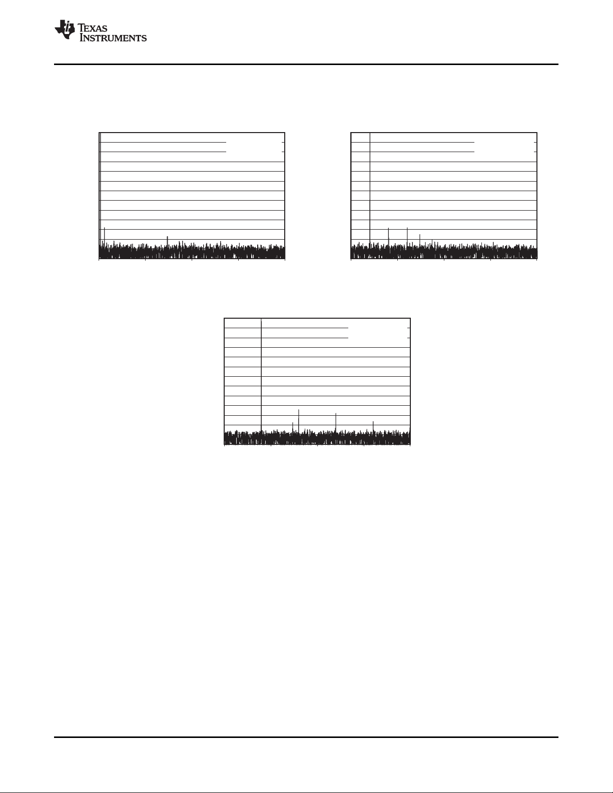
TRANSITION NOISE
Apply a dc input to the ADS8517 and initiate 1000 conversions. The digital output of the converter varies in
output codes because of the internal noise of the ADS8517. This variance is true for all 16-bit SAR converters.
The transition noise specification found in the Electrical Characteristics section is a statistical figure that
represents the one sigma limit or rms value of these output codes.
Using a histogram to plot the output codes, the distribution should appear bell-shaped, with the peak of the bell
curve representing the nominal output code for the input voltage value. The ± 1 σ , ± 2 σ , and ± 3 σ distributions
represent 68.3%, 95.5%, and 99.7%, respectively, of all codes. Multiplying the transition noise (TN) by 6 yields
the ± 3 σ distribution, or 99.7%, of all codes. Statistically, up to three codes could fall outside the five-code
distribution when executing 1000 conversions. The ADS8517 has a TN of 0.8 LSBs, which yields five output
codes for a ± 3 σ distribution. Figure 43 shows 16,384 conversion histogram results.
Figure 43. Histogram of 16,384 Conversions with V
= 0 V in ± 10 V Bipolar Range
IN
AVERAGING
The noise of the converter can be compensated by averaging the digital codes. By averaging conversion results,
transition noise is reduced by a factor of 1/ √ n where n is the number of averages. For example, averaging four
conversion results reduces the TN by 1/2 to 0.4 LSBs. Averaging should only be used for input signals with
frequencies near dc.
For ac signals, a digital filter can be used to low-pass filter and decimate the output codes. This action works in a
similar manner to averaging: for every decimation by 2, the signal-to-noise ratio improves by 3 dB.
Product Folder Link(s): ADS8517
28 Submit Documentation Feedback Copyright © 2008, Texas Instruments Incorporated
Page 29

Microcontroller
SPISlave
CPOL=0(inactiveSCLKisLOW)
CPHA=0or1(datavalidoneitherSCLKedge)
NOTE:
ADS8517
SPIMaster
TOUT
SS
MOSI
SCLK
R/C
BUSY
SDATA
DATACLK
EXT/INT
CS
BYTE
ADS8517
www.ti.com
.......................................................................................................................................................................................... SLAS527 – SEPTEMBER 2008
ADS8517 AS AN SPI MASTER DEVICE (INT/ EXT TIED LOW)
Figure 44 shows a simple interface between the ADS8517 and an SPI-equipped microcontroller or TMS320
series digital signal processor (DSP) when using the internal serial data clock. This interface assumes that the
microcontroller or DSP is configured as an SPI slave, is capable of receiving 16-bit transfers, and that the
ADS8517 is the only serial peripheral on the SPI bus.
Figure 44. ADS8517 as SPI Master
To maintain synchronization with the ADS8517, the microcontroller slave select ( SS) input should be connected
to the BUSY output of the ADS8517. When a transition from high-to-low occurs on BUSY (indicating the current
conversion is in process), the ADS8517 internal SCLK begins shifting the previous conversion data into the
MOSI pin of the microcontroller. In this scenario, the CONV input to the ADS8517 can be controlled from an
external trigger source, or a trigger generated by the microcontroller. The ADS8517 internal SCLK provides 2 ns
(min) of setup time and 41 ns (min) of hold time on the SDATA output (see td5and td6in Table 6 ), allowing the
microcontroller to sample data on either the rising or falling edge of SCLK.
Copyright © 2008, Texas Instruments Incorporated Submit Documentation Feedback 29
Product Folder Link(s): ADS8517
Page 30

Microcontroller
SPIMaster
CPOL=0(inactiveSCLKisLOW)
CPHA=1(datavalidonSCLKfallingedge)
NOTE:
ADS8517
SPISlave
TOUT
INT
MOSI
SCLK
R/C
BUSY
SDATA
DATACLK
CS
EXT/INT
V
S
BYTE
ADS8517
SLAS527 – SEPTEMBER 2008 ..........................................................................................................................................................................................
www.ti.com
ADS8517 AS AN SPI SLAVE DEVICE (INT/ EXT TIED HIGH)
Figure 45 shows another interface between the ADS8517 and an SPI-equipped microcontroller or DSP in which
the host processor acts as an SPI master device.
Figure 45. ADS8517 as SPI Slave
In this configuration, the data transfer from the ADS8517 is triggered by the rising edge of the serial data clock
provided by the SPI master. The SPI interface should be configured to read valid SDATA on the falling edge of
SCLK. When a minimum of 17 SCLKs are provided to the ADS8517, data can be strobed to the host processor
on the rising SCLK edge providing a 2ns (min) hold time (see td8in Table 6 ).
When using an external interrupt to facilitate serial data transfers, as shown in Figure 45 , there are two options
for the configuration of the interrupt service routine (ISR): falling-edge-triggered or rising-edge-triggered.
A falling-edge-triggered transfer would initiate an SPI transfer after the falling edge of BUSY, providing the host
controller with the previous conversion results, while the current conversion cycle is underway. The timing for this
type of interface is described in detail in Figure 36 . Care must be taken to ensure the entire 16-bit conversion
result is retrieved from the ADS8517 before BUSY returns high to avoid the potential corruption of the current
conversion cycle.
A rising-edge-triggered transfer is the preferred method of obtaining the conversion results. This timing is
depicted in Figure 35 . This method of obtaining data ensures that SCLK is static during the conversion cycle and
provides the host processor with current cycle conversion results.
8-BIT SPI INTERFACE
For microcontrollers that only support 8-bit SPI transfers, it is recommended to configure the ADS8517 for SPI
slave operation, as depicted in Figure 45 . With the microcontroller configured as the SPI master, two 8-bit
transfers are required to obtain full 16-bit conversion results from the ADS8517. The eight MSBs of the
conversion result are considered valid on the falling SCLK edges of the first transfer, with the remaining four
LSBs being valid on the first four falling SCLK edges in the second transfer.
30 Submit Documentation Feedback Copyright © 2008, Texas Instruments Incorporated
Product Folder Link(s): ADS8517
Page 31

PACKAGE OPTION ADDENDUM
www.ti.com
13-Nov-2008
PACKAGING INFORMATION
Orderable Device Status
(1)
Package
Type
Package
Drawing
Pins Package
Qty
Eco Plan
ADS8517IBDW ACTIVE SOIC DW 28 20 Green (RoHS &
no Sb/Br)
ADS8517IBDWG4 ACTIVE SOIC DW 28 20 Green (RoHS &
no Sb/Br)
ADS8517IBDWR ACTIVE SOIC DW 28 1000 Green (RoHS &
no Sb/Br)
ADS8517IBDWRG4 ACTIVE SOIC DW 28 1000 Green (RoHS &
no Sb/Br)
ADS8517IBPW PREVIEW TSSOP PW 28 50 TBD Call TI Call TI
ADS8517IBPWR PREVIEW TSSOP PW 28 2000 TBD Call TI Call TI
ADS8517IDW ACTIVE SOIC DW 28 20 Green (RoHS &
no Sb/Br)
ADS8517IDWG4 ACTIVE SOIC DW 28 20 Green (RoHS &
no Sb/Br)
ADS8517IDWR ACTIVE SOIC DW 28 1000 Green (RoHS &
no Sb/Br)
ADS8517IDWRG4 ACTIVE SOIC DW 28 1000 Green (RoHS &
no Sb/Br)
ADS8517IPW PREVIEW TSSOP PW 28 50 TBD Call TI Call TI
ADS8517IPWR PREVIEW TSSOP PW 28 2000 TBD Call TI Call TI
(1)
The marketing status values are defined as follows:
ACTIVE: Product device recommended for new designs.
LIFEBUY: TI has announced that the device will be discontinued, and a lifetime-buy period is in effect.
NRND: Not recommended for new designs. Device is in production to support existing customers, but TI does not recommend using this part in
a new design.
PREVIEW: Device has been announced but is not in production. Samples may or may not be available.
OBSOLETE: TI has discontinued the production of the device.
(2)
Lead/Ball Finish MSL Peak Temp
CU NIPDAU Level-2-260C-1 YEAR
CU NIPDAU Level-2-260C-1 YEAR
CU NIPDAU Level-2-260C-1 YEAR
CU NIPDAU Level-2-260C-1 YEAR
CU NIPDAU Level-2-260C-1 YEAR
CU NIPDAU Level-2-260C-1 YEAR
CU NIPDAU Level-2-260C-1 YEAR
CU NIPDAU Level-2-260C-1 YEAR
(3)
(2)
Eco Plan - The planned eco-friendly classification: Pb-Free (RoHS), Pb-Free (RoHS Exempt), or Green (RoHS & no Sb/Br) - please check
http://www.ti.com/productcontent for the latest availability information and additional product content details.
TBD: The Pb-Free/Green conversion plan has not been defined.
Pb-Free (RoHS): TI's terms "Lead-Free" or "Pb-Free" mean semiconductor products that are compatible with the current RoHS requirements
for all 6 substances, including the requirement that lead not exceed 0.1% by weight in homogeneous materials. Where designed to be soldered
at high temperatures, TI Pb-Free products are suitable for use in specified lead-free processes.
Pb-Free (RoHS Exempt): This component has a RoHS exemption for either 1) lead-based flip-chip solder bumps used between the die and
package, or 2) lead-based die adhesive used between the die and leadframe. The component is otherwise considered Pb-Free (RoHS
compatible) as defined above.
Green (RoHS & no Sb/Br): TI defines "Green" to mean Pb-Free (RoHS compatible), and free of Bromine (Br) and Antimony (Sb) based flame
retardants (Br or Sb do not exceed 0.1% by weight in homogeneous material)
(3)
MSL, Peak Temp. -- The Moisture Sensitivity Level rating according to the JEDEC industry standard classifications, and peak solder
temperature.
Important Information and Disclaimer:The information provided on this page represents TI's knowledge and belief as of the date that it is
provided. TI bases its knowledge and belief on information provided by third parties, and makes no representation or warranty as to the
accuracy of such information. Efforts are underway to better integrate information from third parties. TI has taken and continues to take
reasonable steps to provide representative and accurate information but may not have conducted destructive testing or chemical analysis on
incoming materials and chemicals. TI and TI suppliers consider certain information to be proprietary, and thus CAS numbers and other limited
information may not be available for release.
In no event shall TI's liability arising out of such information exceed the total purchase price of the TI part(s) at issue in this document sold by TI
to Customer on an annual basis.
Addendum-Page 1
Page 32

PACKAGE OPTION ADDENDUM
www.ti.com
13-Nov-2008
Addendum-Page 2
Page 33

PACKAGE MATERIALS INFORMATION
www.ti.com
TAPE AND REEL INFORMATION
6-Nov-2008
*All dimensions are nominal
Device Package
ADS8517IBDWR SOIC DW 28 1000 330.0 32.4 11.35 18.67 3.1 16.0 32.0 Q1
ADS8517IDWR SOIC DW 28 1000 330.0 32.4 11.35 18.67 3.1 16.0 32.0 Q1
Type
Package
Drawing
Pins SPQ Reel
Diameter
(mm)
Reel
Width
W1 (mm)
A0 (mm) B0 (mm) K0 (mm) P1
(mm)W(mm)
Pin1
Quadrant
Pack Materials-Page 1
Page 34
PACKAGE MATERIALS INFORMATION
www.ti.com
6-Nov-2008
*All dimensions are nominal
Device Package Type Package Drawing Pins SPQ Length (mm) Width (mm) Height (mm)
ADS8517IBDWR SOIC DW 28 1000 346.0 346.0 49.0
ADS8517IDWR SOIC DW 28 1000 346.0 346.0 49.0
Pack Materials-Page 2
Page 35

Page 36

MECHANICAL DATA
MTSS001C – JANUARY 1995 – REVISED FEBRUARY 1999
PW (R-PDSO-G**) PLASTIC SMALL-OUTLINE P ACKAGE
14 PINS SHOWN
0,65
1,20 MAX
14
0,30
0,19
8
4,50
4,30
PINS **
7
Seating Plane
0,15
0,05
8
1
A
DIM
6,60
6,20
14
0,10
M
0,10
0,15 NOM
0°–8°
2016
Gage Plane
24
0,25
0,75
0,50
28
A MAX
A MIN
NOTES: A. All linear dimensions are in millimeters.
B. This drawing is subject to change without notice.
C. Body dimensions do not include mold flash or protrusion not to exceed 0,15.
D. Falls within JEDEC MO-153
3,10
2,90
5,10
4,90
5,10
4,90
6,60
6,40
7,90
7,70
9,80
9,60
4040064/F 01/97
POST OFFICE BOX 655303 • DALLAS, TEXAS 75265
Page 37

IMPORTANT NOTICE
Texas Instruments Incorporated and its subsidiaries (TI) reserve the right to make corrections, modifications, enhancements, improvements,
and other changes to its products and services at any time and to discontinue any product or service without notice. Customers should
obtain the latest relevant information before placing orders and should verify that such information is current and complete. All products are
sold subject to TI’s terms and conditions of sale supplied at the time of order acknowledgment.
TI warrants performance of its hardware products to the specifications applicable at the time of sale in accordance with TI’s standard
warranty. Testing and other quality control techniques are used to the extent TI deems necessary to support this warranty. Except where
mandated by government requirements, testing of all parameters of each product is not necessarily performed.
TI assumes no liability for applications assistance or customer product design. Customers are responsible for their products and
applications using TI components. To minimize the risks associated with customer products and applications, customers should provide
adequate design and operating safeguards.
TI does not warrant or represent that any license, either express or implied, is granted under any TI patent right, copyright, mask work right,
or other TI intellectual property right relating to any combination, machine, or process in which TI products or services are used. Information
published by TI regarding third-party products or services does not constitute a license from TI to use such products or services or a
warranty or endorsement thereof. Use of such information may require a license from a third party under the patents or other intellectual
property of the third party, or a license from TI under the patents or other intellectual property of TI.
Reproduction of TI information in TI data books or data sheets is permissible only if reproduction is without alteration and is accompanied
by all associated warranties, conditions, limitations, and notices. Reproduction of this information with alteration is an unfair and deceptive
business practice. TI is not responsible or liable for such altered documentation. Information of third parties may be subject to additional
restrictions.
Resale of TI products or services with statements different from or beyond the parameters stated by TI for that product or service voids all
express and any implied warranties for the associated TI product or service and is an unfair and deceptive business practice. TI is not
responsible or liable for any such statements.
TI products are not authorized for use in safety-critical applications (such as life support) where a failure of the TI product would reasonably
be expected to cause severe personal injury or death, unless officers of the parties have executed an agreement specifically governing
such use. Buyers represent that they have all necessary expertise in the safety and regulatory ramifications of their applications, and
acknowledge and agree that they are solely responsible for all legal, regulatory and safety-related requirements concerning their products
and any use of TI products in such safety-critical applications, notwithstanding any applications-related information or support that may be
provided by TI. Further, Buyers must fully indemnify TI and its representatives against any damages arising out of the use of TI products in
such safety-critical applications.
TI products are neither designed nor intended for use in military/aerospace applications or environments unless the TI products are
specifically designated by TI as military-grade or "enhanced plastic." Only products designated by TI as military-grade meet military
specifications. Buyers acknowledge and agree that any such use of TI products which TI has not designated as military-grade is solely at
the Buyer's risk, and that they are solely responsible for compliance with all legal and regulatory requirements in connection with such use.
TI products are neither designed nor intended for use in automotive applications or environments unless the specific TI products are
designated by TI as compliant with ISO/TS 16949 requirements. Buyers acknowledge and agree that, if they use any non-designated
products in automotive applications, TI will not be responsible for any failure to meet such requirements.
Following are URLs where you can obtain information on other Texas Instruments products and application solutions:
Products Applications
Amplifiers amplifier.ti.com Audio www.ti.com/audio
Data Converters dataconverter.ti.com Automotive www.ti.com/automotive
DSP dsp.ti.com Broadband www.ti.com/broadband
Clocks and Timers www.ti.com/clocks Digital Control www.ti.com/digitalcontrol
Interface interface.ti.com Medical www.ti.com/medical
Logic logic.ti.com Military www.ti.com/military
Power Mgmt power.ti.com Optical Networking www.ti.com/opticalnetwork
Microcontrollers microcontroller.ti.com Security www.ti.com/security
RFID www.ti-rfid.com Telephony www.ti.com/telephony
RF/IF and ZigBee® Solutions www.ti.com/lprf Video & Imaging www.ti.com/video
Mailing Address: Texas Instruments, Post Office Box 655303, Dallas, Texas 75265
Copyright © 2008, Texas Instruments Incorporated
Wireless www.ti.com/wireless
 Loading...