

Page 1

User's Guide
SLAU189 – September 2006
ADS8364/65MEVM
This user's guide describes the characteristics, operation, and use of the
ADS8364/65MEVM 16-bit, parallel analog-to-digital converter evaluation module
(EVM). A complete circuit description, a schematic diagram, and bill of materials is
included.
Contents
1 EVM Overview ...................................................................................... 1
2 Introduction .......................................................................................... 2
3 Analog Interface .................................................................................... 2
4 Digital Interface ..................................................................................... 4
5 Power Supplies ..................................................................................... 6
6 EVM Operation ...................................................................................... 6
7 EVM Bill of Materials, Assembly Drawing, and Schematic .................................... 7
8 Related Documentation From Texas Instruments ............................................ 10
List of Figures
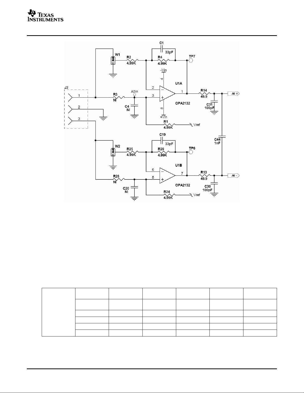
1 Channel A0 Input Circuit ........................................................................... 3
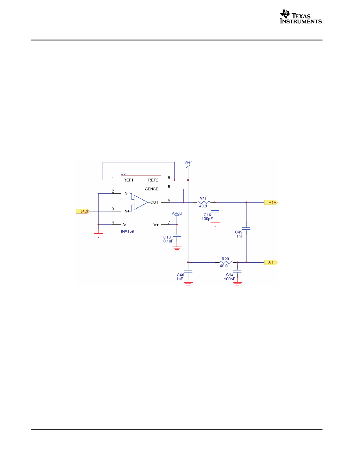
2 Channel A1 Input Circuit ........................................................................... 4
3 ADS8364/654MEVM Assembly Drawing ........................................................ 9
1 EVM Overview
1.1 Features
List of Tables
1 Typical Analog Input Buffer Circuit Values ...................................................... 3
2 Header/Socket Combinations at J5 .............................................................. 5
3 J1 Pinout and Functions ........................................................................... 6
4 JP1 Pinout ........................................................................................... 6
5 ADS8364/65MEVM Jumpers ...................................................................... 7
6 ADS8364/65MEVM Bill of Materials ............................................................. 7
• Full-featured evaluation board for the ADS8364 and ADS8365 250-kHz, 16-bit, 6-channel,
simultaneous-sampling, analog-to-digital converter
• Analog inputs can be configured as single-ended or differential
• Modular design allows direct connection to various DSP platforms through the 5-6K and HPA-MCU
Interface Boards
• Built-in reference
• High-speed parallel interface
SLAU189 – September 2006 ADS8364/65MEVM 1
Submit Documentation Feedback
Page 2

www.ti.com
Introduction
2 Introduction
The ADS8364 and ADS8365 are high-speed, low-power, 6-channel, 16-bit A/D converters that operate
from independent +5-V Avdd and Dvdd supplies. Internal buffer circuits powered from 3.3-V to 5.5-V BVdd
supplies allow for mixed logic level operation without additional level translation.
The six input channels contain fully differential sample-and-hold circuits which are divided into three pairs
(A, B, and C). Each channel pair has a hold signal (HOLDA, HOLDB, and HOLDC) which, when strobed
together, provides simultaneous sampling on all six analog inputs. The devices accept analog input
voltages in the range of –V
circuit is used in the analog front-end circuitry (see Figure 1 ).
Conversion time for the ADS8364 and ADS8365 is 3.2 µ s when a 5-MHz external clock is used. The
corresponding acquisition time is 800 ns. To achieve maximum output rate (250 kHz per channel, effective
1.5-MSPS throughput max), the read function can be performed during the start of the next conversion.
3 Analog Interface
The analog input to the EVM is divided in two parts. Connector J4 provides access to input channels A0
and A1 through two different amplifier circuit configurations. The input buffer configuration of channel A0
presents a typical front-end circuit for the A/D converter. Its function is to provide level and impedance
adaptation of the input signal. The input to channel A1 is a bipolar configuration using the INA159 to
accommodate ± 10-V input signals. Connector J3 provides access to the remaining analog input channels
through simple R/C filters.
3.1 Analog Input – Channel A0
The analog input to the ADS8364/65MEVM board for channel A0 is composed of the dual OPA2132
operational amplifier and its associated circuitry as shown in Figure 1 . The OPA2132 is powered from the
± 12-V analog supply, and arranged as an inverting amplifier with a gain of 1. The internal +2.5-V
reference voltage of the ADS8364 or ADS8365 is applied to the noninverting input of the OPA2132 to
provide input bias.
to +V
REF
. The parts also accept bipolar input ranges when a level shift
REF
2 ADS8364/65MEVM SLAU189 – September 2006
Submit Documentation Feedback
Page 3
www.ti.com
Analog Interface
NOTE: Components marked NI are NOT INSTALLED.
This configuration allows single-ended signals of ± 2.5 V (+5 Vpp) to be applied to either input of channel
A0 (J2 pin 1 or 3 referenced to pin 2). The input also can be applied to connector J4 (not shown) pins 2 or
4, referenced to analog ground.
3.2 Bipolar Input to Channel A0
By changing components and setting the appropriate jumper, it is possible to configure the input buffer to
accept bipolar input voltages. Table 1 is related to the schematic presented in Figure 1 and represents just
a few of the possible input configurations.
Input Voltage R3 R2 R1 R4 W2
Refer to Figure 1 Default open 5k Ω 5k Ω 5 k Ω 1–2
0 – +5
0 – 2.5 5 k Ω 5 k Ω open 5 k Ω 2–3
– 2.5 – +2.5 20 k Ω 4 k Ω 20 k Ω 4 k Ω 2–3
– 5 – +5 20 k Ω 4 k Ω 10 k Ω 2 k Ω 2–3
– 10 – +10 20 k Ω 4 k Ω 5 k Ω 1 k Ω 2–3
Figure 1. Channel A0 Input Circuit
Table 1. Typical Analog Input Buffer Circuit Values
R28 R25 R24 R29 W1
SLAU189 – September 2006 ADS8364/65MEVM 3
Submit Documentation Feedback
Page 4
www.ti.com
Digital Interface
The output from the buffer stage in each case applies 0-5 V to the CHA0(+) input when the applied signal
is connected to J2 pin 1 or J4 pin 2. The applied signal is directed to the CHA0(-) input when connected
via J2 pin 3 or J4 pin 4.
When operating the ADS836x with single-ended signals, it is important to keep the unused ADC input
biased to +2.5 V. This is easily accomplished on the EVM by changing the components associated with
either the inverting or noninverting input only, leaving the default component values shown in Table 1 on
the unused input. For example, to achieve a bipolar input range of ± 10 V on CHA0(+), use the component
values shown for R1–R4 and move the shunt on W2 position 2-3. Components R24, R25, R28, and R29
and the shunt on W1 should remain in the default conditions shown in Table 1 .
3.3 Analog Input – Channel A1
The analog input to the ADS8364/65MEVM board for channel A1 is composed of the INA159 difference
amplifier and the associated circuitry as shown in Figure 2 . The INA159 is powered from the +5-V analog
supply, and arranged as a noninverting amplifier with a gain of 0.2. The internal +2.5-V reference voltage
of the ADS836x is applied to both REF1 and REF2 pins of the INA159 to provide a direct ± 10-V interface
with built-in level translation to the noninverting input of channel A1.
Figure 2. Channel A1 Input Circuit
3.4 Analog Inputs –Channels B0/B1 and C0/C1
The analog inputs to the remaining ADS836x input channels are routed to connector J3 and configured
with simple R/C filters only. This configuration allows the EVM user to apply any customized input circuit to
the data converter. Connector J3 is composed of a male/female pass-through combination of pin header
and socket with industry standard 0.1-inch centers.
When the ADS8364/65MEVM is used in combination with the 5-6K Interface Board or HPA-MCU Interface
Board, the DAP Signal Conditioning Board (SLAU105 ) can be used to drive the remaining input channels.
4 Digital Interface
The ADS8364/65MEVM is designed for easy interfacing to multiple control platforms. Jumper options are
provided on the EVM to allow control over the state of Chip Select pin ( CS) as well as the operating mode
pins (A0–A2), the Reset pin ( RST), and the Conversion Start strobes (HOLD A, HOLDB, and HOLDC).
4 ADS8364/65MEVM SLAU189 – September 2006
Submit Documentation Feedback
Page 5

www.ti.com
4.1 Parallel Control
Digital Interface
Jumpers W4 and W6 control the signals applied to A0, A1, A2, and CS. In the factory default mode, W6 is
closed by means of a shunt jumper. The Ax and CS pins are controlled by the signals applied to J5 (top or
bottom side). When used with either the 5-6K or HPA-MCU Interface Boards, these control signals are
associated with the host processors address bus.
By removing the shunt jumper located at W6, the A0, A1, and A2 pins are controlled by shunt jumpers
placed on W4. The CS pin is routed to J5.1, which requires the application of an active-low Chip Select
signal. A simple shunt jumper placed across J5 pins 1-2 can be used to force the CS pin to ground if
desired.
Samtec part numbers SSW-110-22-F-D-VS-K and TSM-110-01-T-DV-P provide a convenient 10-pin,
dual-row, header/socket combination at J5 (Table 2 ). This header/socket provides access to the digital
control pins of the EVM. Consult Samtec at www.samtec.com or 1-800-SAMTEC-9 for a variety of mating
connector options.
Table 2. Header/Socket Combinations at J5
Pin Number Signal Description
J5.1 DC_CSa Daughter Card Chip Select – active-low signal used to access the EVM
J5.3 DC_AWE Write Strobe – signal not used on the ADS8364/65M EVM
J5.5 DC_ARE Read Strobe – active-low signal used to access parallel data
J5.7 EVM_A0 EVM Address line 0 – used with U3 to control A0
J5.9 EVM_A1 EVM Address line 1 – used with U3 to control A1
J5.11 EVM_A2 EVM Address line 2 – used with U3 to control A2
J5.13 EVM_A3 EVM Address line 3 – used with U3 and U6 to control CS
J5.15 EVM_A4 EVM Address line 4 – not used
J5.17 DC_TOUT Timer Input – optional CLK input used with W8
J5.19 DC_INTa Interrupt Output to Host Processor – connects to the ADC EOC pin
4.2 Parallel Data
The ADS8364/65MEVM uses Samtec part numbers SSW-116-22-F-D-VS-K and TSM-116-01-T-DV-P to
provide a convenient 16-pin, dual-row header/socket combination at J6. This header/socket combination
provides access to the parallel data pins of the ADS7864. Data line D0 is connected to J6 pin 1. Data
lines 1–15 are located on pins 3–31, respectively. Even pin numbers 2–32 are connected to digital ground.
4.3 GPIO/Control Options
Samtec part numbers SSW-110-22-F-D-VS-K and TSM-110-01-T-DV-P provide a 10-pin, dual-row,
header/socket combination at J1 to facilitate general-purpose input/output (GPIO) control options to the
ADS836x device installed on the EVM. Table 3 describes the functions and pinout of J1.
SLAU189 – September 2006 ADS8364/65MEVM 5
Submit Documentation Feedback
Page 6

www.ti.com
Power Supplies
5 Power Supplies
Table 3. J1 Pinout and Functions
Pin Number Signal Description
J1.1 NAP Controls power-down options on the ADS8365 (only) using the NAP input pin
J1.3 ADD Controls read options, when HI, address information can be read from the chip
J1.5 HOLD_C# Active-low signal HOLDC used to start a conversion on ADC channel pair C
J1.7 HOLD_B# Active-low signal HOLDB used to start a conversion on ADC channel pair B
J1.9 HOLD_A# Active-low signal HOLDA used to start a conversion on ADC channel pair A
J1.11 RESET# Active-low signal RESET used to place the ADS7864’s FIFO in reset state
J1.13 NA Unused on the ADS8364/65MEVM
J1.15 NA Unused on the ADS8364/65MEVM
J1.17 DC_TOUTa Used with W10 to allow host processor timer control of HOLDx
J1.19 NA Unused on the ADS8364/65MEVM
The ADS8364/65MEVM board requires +5 VDC for the both the analog and digital section of the ADC.
The supply (+Va and +Vd) can range from +4.75 VDC to +5.25 VDC. . The internal buffer can be powered
through the BVdd input voltage and can range from 2.7 VDC to 5.5 VDC. Because the EVM is designed to
work with the 5-6K and HPA-MCU Interface Boards, JP1 provides direct connection to the common power
bus described in SLAU104 .
Table 4 shows the pinout of JP1:
Alternate power sources can be applied via various test points located on the EVM. See the schematic at
the end of this document for details. Note – while filters are provided for all power supply inputs, optimal
performance of the EVM requires a clean, well-regulated power source.
5.1 Reference Voltages
The ADS8364/65MEVM is configured to use its internal reference through jumper W3 (see schematic for
details). If an external reference is desired, the shunt jumper on W3 should be moved to cover pins 1-2;
the external reference source can be applied to the test point labeled TP10 referenced to TP12. The
internal +2.5-V reference is still connected to the input buffer U1 in this case to ensure proper mid-point
biasing to channel A1.
6 EVM Operation
The analog input swing is 5 Vpp, centered on a +2.5-V internal or external reference. The installed device
accepts bipolar input ranges when a level shift circuit is used in the analog front-end circuitry. For
information on various circuit configurations, see section 3.2 of this document or section 12 of Op-Amps
for Everyone (SLOD006 ) .
Once power is applied to the EVM, the analog input source can be connected directly to J3 or J4 (top or
bottom side) or through optional amplifier and signal-conditioning modules using the 5-6K and HPA-MCU
Interface Boards. The analog input level should not exceed 5 Vp-p. The analog input range is from ± Vref
(typically 2.5 VDC) centered at +2.5 V.
Table 4. JP1 Pinout
Signal Pin Number Signal
+VA (positive input buffer supply) 1 2 -VA (negative input buffer supply)
+5VA (+Va to the ADS8364) 3 4 -5VA (Unused)
DGND 5 6 AGND
+1.8VD (Unused) 7 8 +VD1 (Unused)
+3.3VD (used with W5 for support circuitry) 9 10 +5VD (+5V to pin 22 of the ADS8364 and pin 22 of the
ADS8365)
6 ADS8364/65MEVM SLAU189 – September 2006
Submit Documentation Feedback
Page 7

www.ti.com
The digital control signals can be applied directly to J1 and J5 (top or bottom side). The
ADS8364/65MEVM can also be connected directly to the 5-6K Interface Board for use with a variety of
C5000™ and C6000™ series DSP Starter Kits (DSK), or the HPA-MCU Interface Board for use with
C2000™ Series DSPs and TMS470™ Series controllers. The Control and Data connectors are designed
to allow pattern generators and/or logic analyzers to be connected to the EVM using standard ribbon-type
cables on 0.1-inch centers.
The BYTE signal, which controls the output of the ADS836x when used with 8-bit controllers, can be
manipulated with jumper W7. By default, W7 is closed and the BYTE pin is held low, providing data in
16-bit format. Removing the shunt at W7 asserts BYTE high by means of pullup resistor R23.
The conversion clock can be applied to J7, a BNC connector with a 50- Ω terminator, or J5 as mentioned
previously. Jumper W8 allows the EVM user to select the clock source. In normal operation (factory
default) the shunt on jumper W8 is covering pins 2-3. To use a clock source applied to the BNC connector
J7, move the shunt at jumper W8 to cover pins 1-2. In either case, the conversion clock can be monitored
at TP21.
6.1 Default Jumper Locations
Table 5 provides a list of jumpers found on the EVM and their factory default conditions.
Jumper Shunt Position Jumper Description
W1 Pins 1-2 Controls CHA1(+) input source selection
W2 Pins 1-2 Controls CHA1(–) input source selection
W3 Pins 2-3 Controls reference source (default is internal)
W4 OPEN 3x2 Jumper to control A0, A1, A2
W5 Pins 1-2 Controls BVdd Selection
W6 Closed Controls application of A0, A1 and A2 signals as well as the chip select input. Used in conjunction
W7 Closed Controls BYTE input, opening W7 forces BYTE high via R23
W8 Pins 2-3 Controls application of conversion clock source via J5 or J7
W9 NA W9 pins 2-3 are wired short on the PWB
W10 TIMER 3 × 3 Jumper to control HOLDx signals – timer or GPIO options available
EVM Bill of Materials, Assembly Drawing, and Schematic
Table 5. ADS8364/65MEVM Jumpers
with W4.
7 EVM Bill of Materials, Assembly Drawing, and Schematic
7.1 Bill of Materials
Table 6 contains a complete Bill of Materials for the ADS8364/65MEVM.
Table 6. ADS8364/65MEVM Bill of Materials
Designators Description Manufacturer Mfg. Part Number
C2 C3 C7 C10–C12 0.1uF, 0603, Ceramic, X7R, 25V, 10% TDK Corp. C1608X7R1E104K
C18 C37–C39 C41
C45–C49 C52
C35 C36 C42–C44 1nF, 0603, Ceramic, COG, 50V, 5% TDK Corp. C1608C0G1H102J
C53
C5 C6 C8 C9 C13 10 µ F, 0805, Ceramic, X5R, 16V, 10% Taiyo Yuden EMK212BJ106KG-T
C15
C1 C19 33pF, 0805, Ceramic, COG, 50V, 5% TDK Corp. C1608C0G1H330J
C22 C24 0.01 µ F, 0603, Ceramic, COG, 25V, 5% TDK Corp. C1608C0G1E103J
C16 C14 C25–C34 100pF, 0603, Ceramic, COG, 50V, 5% TDK Corp. C1608C0G1H101J
C50 1 µ F, 0603, Ceramic, X7R, 16V, 10% TDK Corp. C1608X7R1C105K
SLAU189 – September 2006 ADS8364/65MEVM 7
Submit Documentation Feedback
Page 8

www.ti.com
EVM Bill of Materials, Assembly Drawing, and Schematic
Table 6. ADS8364/65MEVM Bill of Materials (continued)
Designators Description Manufacturer Mfg. Part Number
D1 D2 Green LED Chicago Miniature CMD15-21VGC/TR8
J1 J3–J5(Bottom 10 Pin, Dual Row, SMT Socket (20 Pos.) Samtec SSW-110-22-S-D-VS
Side)
J1 J3–J5 (Top Side) 10 Pin, Dual Row, SMT Header (20 Pos.) Samtec TSM-110-01-T-D-V-P
J2 3 Terminal Screw Connector On-Shore Tech. ED555/3DS
J6 (Bottom Side) 16 Pin, Dual Row, SMT Socket (32 Pos.) Samtec SSW-116-22-S-D-VS
J6 (Top Side) 16 Pin, Dual Row, SMT Header (32 Pos.) Samtec TSM-116-01-T-D-V-P
J7 PCB Mount BNC Amphenol 31-5329
JP1(Bottom Side) 5 Pin, Dual Row, SMT Socket (10 Pos.) Samtec SSW-105-22-S-D-VS
JP1 (Top Side) 5 Pin, Dual Row, SMT Header (10 Pos.) Samtec TSM-105-01-T-D-V-P
FB1–FB5 0805 size Ferrite Bead TDK Corp. MMZ2012D121B
R1 R2 R4 R24 R25 4.99k Ω , 1%, 0805, .1W Resistor Yageo Corp. 9C08052A4991FKHFT
R29
R5–R14 R20 R21 49.9 Ω , 0603, 1%, 0.1W Resistor Yageo Corp. RC0603FR-0749R9L
R31 R36
R16–R19 R22 R23 10k Ω , 0603, 5%, 0.1W Resistor Yageo Corp. RC0603JR-0710KL
R34 R35
R26 R27 2k Ω , 0805, 0.1W Resistor Yageo Corp. 9C08052A2001JLHFT
R15 R32 0 Ω , 0603, 0.1W Resistor Yageo Corp. RC0603JR-070RL
TP1–TP3 TP8 Tp9 Red Test Point Loop Keystone 5000
TP10 TP20
AGND DGND TP12 Black Test Point Loop Keystone 5001
TP11 TP13–TP17 SMT Test Point Loop – Shown on Silkscreen as: A0, Keystone 5015
TP21–TP24 A1, A2, RST, RD, WR, CS, CLOCK, FD, EOC
U1 OPA2132, SOIC Texas Instruments OPA2132UA
U2 OPA2340; DGK package Texas Instruments OPA2340EA
U4 ADS8364 Texas Instruments ADS8364Y/250
U5 INA159; DGK package Texas Instruments INA159AIDGKR
U3 SN74CBT3257PW Texas Instruments SN74CBT3257PWR
U6 SN74AHC1G04 Texas Instruments SN74AHC1G04DBVT
U7 SN74AHC125 Texas Instruments SN74AHC125PW
W1–W3 W5 W8 3 Pin Header Samtec TSW-103-07-L-S
W6 W7 2 Pin Header Samtec TSW-102-07-L-S
W4 2 × 3 Header Samtec TSW-103-07-L-D
W10 3 × 3 Header Samtec TSM-103-07-L-T
C4 C17 C20 C21 Not Installed
C23 C51 R3 R28
R33 W9
ADS8364/65MEVM 8 SLAU189 – September 2006
Submit Documentation Feedback
Page 9

www.ti.com
7.2 Assembly Drawing
Figure 3 shows the top layer of the ADS8364/65MEVM and provides quick access to component
designator found on the PWB. Complete Gerber files are available on request.
EVM Bill of Materials, Assembly Drawing, and Schematic
Figure 3. ADS8364/654MEVM Assembly Drawing
7.3 Circuit Schematics
The entire circuit schematic for the ADS8364/65MEVM appears on the following page.
SLAU189 – September 2006 ADS8364/65MEVM 9
Submit Documentation Feedback
Page 10

54321
Note:
Components marked "NI"
are NOT installed!
W1
R2
4.99K
D
Op Amp Bypass
+Vin
C24
C23
0.01uF
NI
C22
C21
0.01uF
NI
-Vin
C
J4
1 2
3 4
5 6
7 8
9 10
11 12
13 14
15 16
17 18
19 20
Analog Input
B
R33
NI
AVdd
W9
Wire Short
J2
1
2
3
C17
NI
U5
1
REF1
2
IN-
3
IN+
C51
NI
4
V-
INA159
R3
NI
R28
NI
W2
C4
NI
R25
4.99K
C20
NI
REF2
SENSE
A0In
OUT
V+
C18
0.1uF
C1
33pF
R4
4.99K
-Vin
2
3
8 4
+Vin
R1
4.99K
C19
33pF
R29
4.99K
6
5
R24
4.99K
Vref
8
5
6
AVdd
7
U1A
OPA2132
U1B
OPA2132
R21
49.9
C16
100pF
TP7
R14
1
49.9
C31
100pF
Vref
TP6
R13
7
49.9
C30
100pF
Vref
C53
1nF
C44
1nF
A0+
A0-
A1+
R12
49.9
100pF
R11
49.9
100pF
R9
49.9
100pF
C29
C34
C27
C43
1nF
B0+
B0-
B1+
R8
49.9
R7
49.9
R5
49.9
C26
100pF
C25
100pF
C32
100pF
C42
1nF
REV ECN Number Approved
C0+
C0-
C1+
6
Revision History
D
C
B
R20
49.9
C50
1uF
J3
1 2
3 4
5 6
7 8
9 10
11 12
A
13 14
15 16
17 18
19 20
Analog Input
1 2 3 4 56
C14
100pF
A1-
R10
49.9
100pF
C28
C36
1nF
B1-
C35
1nF
R6
49.9
C33
100pF
C1-
ti
12500 TI Boulevard. Dallas, Texas 75243
Title:
Tom Hendrick
Engineer:
Tom Hendrick B A
Drawn By:
FILE:
mADS8364_2_SH1.Sch
ADS8364/65 Modular Evaluation Module
SIZE:
DATE: REV:
14-Jul-2006
SHEET: OF:
13
A
Page 11

54321
6
ADC Bypass
J5
1 2
3 4
5 6
7 8
9 10
11 12
13 14
15 16
17 18
19 20
Parallel Control
BVdd
C52
0.1uF
147
U7
1
1OE
2
A0
1A
1Y
2Y
3Y
4Y
2OE
3OE
4OE
2A
3A
4A
4
5
A1
10
9
A3
13
12
A2
SN74AHC125
J1
1 2
3 4
5 6
7 8
9 10
11 12
13 14
15 16
17 18
19 20
ADC Control
McBSP 1 Setup
ADD = CLKX1 (GP OUT)
HOLD A# = CLKR1 (GP OUT)
HOLD B# = FSX1 (GP OUT)
HOLD C# = FSR1 (GP OUT)
RESET# = DX1 (GP OUT)
FD = DR1 (GP IN)
D
C
C46
0.1uF
CLK
AVdd
C40
0.1uF
RESET#
ADD
BA2
BA1
BA0
HOLD_A#
HOLD_B#
HOLD_C#
FD
DC_INTa
DC_ARE#
DC_AWE
CS#
DC_D0
DC_D1
DC_D2
DC_D3
DC_D4
DC_D5
DC_D6
DC_D7
DC_D8
DC_D9
DC_D10
DC_D11
DC_D12
DC_D13
DC_D14
DC_D15
/NAP
C39
0.1uF
DC_TOUT
C38
0.1uF
W8
TP21
C37
0.1uF
R31
49.9
BVdd
R34
10K
DC_CSa
DC_AWE
DC_ARE#
A0
A1
A2
A3
DC_TOUT
DC_INTa
EVM_A0
EVM_A1
EVM_A3
EVM_A2
BVdd
R35
10K
DC_TOUTa
3
6
8
11
BVdd
BVdd
R22
10K
W6
4
1A
7
2A
9
3A
12
4A
1
S
BVdd
R16
10K
BA0
J6
1 2
3 4
5 6
7 8
9 10
11 12
13 14
15 16
17 18
19 20
21 22
23 24
25 26
27 28
29 30
31 32
TP22
TP14
TP15
TP13
R19
10K
BA1
BA2
J7
CS#
DC_D0
DC_D1
DC_D2
DC_D3
DC_D4
DC_D5
DC_D6
DC_D7
DC_D8
DC_D9
DC_D10
DC_D11
DC_D12
DC_D13
DC_D14
DC_D15
ADC Data Bus
C12
0.1uF
168
U3
1B1
1B2
2B1
2B2
3B1
3B2
4B1
4B2
/OE
SN74CBT3257PWR
R18
R17
10K
10K
W4
ABC
2
3
5
6
11
10
14
13
15
U6
BVdd
EVM_A0
EVM_A1
EVM_A2
M_A0
M_A1
M_A2
53
24
EVM_A3
SN74X1G04
DC_CSa
M_A0
M_A1
M_A2
/NAP
ADD
GP(CLKR)
GP(FSX)
GP(FSR)
RESET#
GP(CLKR)
GP(FSX)
GP(FSR)
HOLD_A#
HOLD_B#
HOLD_C#
W10
BVdd DVdd
C48
AVdd DVdd BVdd
D
59
13
AVdd
AVdd3AVdd8AVdd
A0+
A0-
A1A1+
B0+
B0-
B1B1+
C0+
C
C0C1-
C1+
TP8
63
A0+
64
A0-
1
A1-
2
A1+
5
A_REF
6
B0+
7
B0-
11
B1-
12
B1+
10
B_REF
16
C0+
17
C0-
18
C1-
19
C1+
15
C_REF
62
REFIN
61
REFOUT
AGND
AGND4AGND9AGND
60
14
U4
ADS8364/65
DGND21BGND25BGND
R15
24
22
28
CLK
BVdd50BVdd
DVdd
ADD
EOC#
RD#
WR#
CS#
D10
D11
D12
D13
D14
D15
BYTE
51
52
53
A2
54
A1
55
A0
56
57
58
26
FD
27
29
30
31
48
D0
47
D1
46
D2
45
D3
44
D4
43
D5
42
D6
41
D7
40
D8
39
D9
38
37
36
35
34
33
23
32
HOLD_A#
HOLD_B#
HOLD_C#
BGND49NAP
RESET#
20
W7
C47
0.1uF
0.1uF
BGND
TP17
TP11
TP24 TP16
BVdd
R23
10K
TP23
0 ohm
BGND
B
EXT. REF.
W3
C45
0.1uF
C7
0.1uF
TP10
TP12
R36
49.9
U2B
3
2
7
OPA2340
5
6
C10
0.1uF
DVdd
C15
10uF
Vref
U2A
1
OPA2340
C8
10uF
AVdd
84
TP9
+3.3VD +5VA +VA -VA -5VA +VD1+1.8VD
FB1
C49
0.1uF
+5VD
JP1
1 2
3 4
5 6
7 8
9 10
D2
Green
AGNDDGND
R26
2K
C6
10uF
+VIN
+5VD
TP2
FB3
C3
0.1uF
+VA
C9
10uF
AVdd
TP3
FB5
C41
0.1uF
+5VA
B
W5
+3.3VD
D1
Green
+5VD
C13
10uF
BVdd
TP20
FB2
C11
0.1uF
R32
A
0 ohm
BGND
R27
2K
C5
10uF
-VIN
TP1
C2
0.1uF
FB4
-VA
Engineer:
Drawn By:
FILE:
Tom Hendrick
Tom Hendrick
A
ti
12500 TI Boulevard. Dallas, Texas 75243
Title:
ADS8364/65 Modular Evaluation Module
SIZE:
DATE: REV:
BA
14-Jul-2006
2
SHEET: OF:
3
1 2 3 4 56
Page 12

www.ti.com
Related Documentation From Texas Instruments
8 Related Documentation From Texas Instruments
1. ADS8364, 250kHz, 16-Bit, 6-Channel Simultaneous Sampling Analog-to-Digital Converters data sheet
(SBAS219 )
2. ADS8365, 250kHz, 16-Bit, 6-Channel Simultaneous Sampling Analog-to-Digital Converter data sheet
(SBAS362 )
3. OPA2132, High-Speed FET-Input Operational Amplifiers data sheet (SBOS054 )
4. INA159, Precision Gain of 0.2 Level Translation Difference Amplifier data sheet (SBOS333 )
5. 5-6K Interface Board User's Guide (SLAU104 )
6. DAP Signal Conditioning Board User's Guide (SLAU105 )
7. × HPA-MCU Interface Board User's Guide (SLAU106 )
8. Designing Modular EVMs for Data Acquisition Products application report (SLAA185 )
9. Data Converters for Industrial Power Management application report (SBAA117 )
10. Op-Amps for Everyone application report (SLOD006 )
10 ADS8364/65MEVM SLAU189 – September 2006
Submit Documentation Feedback
Page 13

EVALUATION BOARD/KIT IMPORTANT NOTICE
Texas Instruments (TI) provides the enclosed product(s) under the following conditions:
This evaluation board/kit is intended for use for ENGINEERING DEVELOPMENT, DEMONSTRATION, OR EVALUATION
PURPOSES ONLY and is not considered by TI to be a finished end-product fit for general consumer use. Persons handling the
product(s) must have electronics training and observe good engineering practice standards. As such, the goods being provided are
not intended to be complete in terms of required design-, marketing-, and/or manufacturing-related protective considerations,
including product safety and environmental measures typically found in end products that incorporate such semiconductor
components or circuit boards. This evaluation board/kit does not fall within the scope of the European Union directives regarding
electromagnetic compatibility, restricted substances (RoHS), recycling (WEEE), FCC, CE or UL, and therefore may not meet the
technical requirements of these directives or other related directives.
Should this evaluation board/kit not meet the specifications indicated in the User’s Guide, the board/kit may be returned within 30
days from the date of delivery for a full refund. THE FOREGOING WARRANTY IS THE EXCLUSIVE WARRANTY MADE BY
SELLER TO BUYER AND IS IN LIEU OF ALL OTHER WARRANTIES, EXPRESSED, IMPLIED, OR STATUTORY, INCLUDING
ANY WARRANTY OF MERCHANTABILITY OR FITNESS FOR ANY PARTICULAR PURPOSE.
The user assumes all responsibility and liability for proper and safe handling of the goods. Further, the user indemnifies TI from all
claims arising from the handling or use of the goods. Due to the open construction of the product, it is the user’s responsibility to
take any and all appropriate precautions with regard to electrostatic discharge.
EXCEPT TO THE EXTENT OF THE INDEMNITY SET FORTH ABOVE, NEITHER PARTY SHALL BE LIABLE TO THE OTHER
FOR ANY INDIRECT, SPECIAL, INCIDENTAL, OR CONSEQUENTIAL DAMAGES.
TI currently deals with a variety of customers for products, and therefore our arrangement with the user is not exclusive.
TI assumes no liability for applications assistance, customer product design, software performance, or infringement of
patents or services described herein.
Please read the User’s Guide and, specifically, the Warnings and Restrictions notice in the User’s Guide prior to handling the
product. This notice contains important safety information about temperatures and voltages. For additional information on TI’s
environmental and/or safety programs, please contact the TI application engineer or visit www.ti.com/esh .
No license is granted under any patent right or other intellectual property right of TI covering or relating to any machine, process, or
combination in which such TI products or services might be or are used.
FCC Warning
This evaluation board/kit is intended for use for ENGINEERING DEVELOPMENT, DEMONSTRATION, OR EVALUATION
PURPOSES ONLY and is not considered by TI to be a finished end-product fit for general consumer use. It generates, uses, and
can radiate radio frequency energy and has not been tested for compliance with the limits of computing devices pursuant to part 15
of FCC rules, which are designed to provide reasonable protection against radio frequency interference. Operation of this
equipment in other environments may cause interference with radio communications, in which case the user at his own expense
will be required to take whatever measures may be required to correct this interference.
EVM WARNINGS AND RESTRICTIONS
It is important to operate this EVM within the input voltage range of -15 V to +15 V and the output voltage range of 0 V to 5 V.
Exceeding the specified input range may cause unexpected operation and/or irreversible damage to the EVM. If there are
questions concerning the input range, please contact a TI field representative prior to connecting the input power.
Applying loads outside of the specified output range may result in unintended operation and/or possible permanent damage to the
EVM. Please consult the EVM User's Guide prior to connecting any load to the EVM output. If there is uncertainty as to the load
specification, please contact a TI field representative.
During normal operation, some circuit components may have case temperatures greater than 85 ° C. The EVM is designed to
operate properly with certain components above 30 ° C as long as the input and output ranges are maintained. These components
include but are not limited to linear regulators, switching transistors, pass transistors, and current sense resistors. These types of
devices can be identified using the EVM schematic located in the EVM User's Guide. When placing measurement probes near
these devices during operation, please be aware that these devices may be very warm to the touch.
Mailing Address: Texas Instruments, Post Office Box 655303, Dallas, Texas 75265
Copyright © 2006, Texas Instruments Incorporated
Page 14

IMPORTANT NOTICE
Texas Instruments Incorporated and its subsidiaries (TI) reserve the right to make corrections, modifications, enhancements,
improvements, and other changes to its products and services at any time and to discontinue any product or service without notice.
Customers should obtain the latest relevant information before placing orders and should verify that such information is current and
complete. All products are sold subject to TI’s terms and conditions of sale supplied at the time of order acknowledgment.
TI warrants performance of its hardware products to the specifications applicable at the time of sale in accordance with TI’s
standard warranty. Testing and other quality control techniques are used to the extent TI deems necessary to support this
warranty. Except where mandated by government requirements, testing of all parameters of each product is not necessarily
performed.
TI assumes no liability for applications assistance or customer product design. Customers are responsible for their products and
applications using TI components. To minimize the risks associated with customer products and applications, customers should
provide adequate design and operating safeguards.
TI does not warrant or represent that any license, either express or implied, is granted under any TI patent right, copyright, mask
work right, or other TI intellectual property right relating to any combination, machine, or process in which TI products or services
are used. Information published by TI regarding third-party products or services does not constitute a license from TI to use such
products or services or a warranty or endorsement thereof. Use of such information may require a license from a third party under
the patents or other intellectual property of the third party, or a license from TI under the patents or other intellectual property of TI.
Reproduction of information in TI data books or data sheets is permissible only if reproduction is without alteration and is
accompanied by all associated warranties, conditions, limitations, and notices. Reproduction of this information with alteration is an
unfair and deceptive business practice. TI is not responsible or liable for such altered documentation.
Resale of TI products or services with statements different from or beyond the parameters stated by TI for that product or service
voids all express and any implied warranties for the associated TI product or service and is an unfair and deceptive business
practice. TI is not responsible or liable for any such statements.
TI products are not authorized for use in safety-critical applications (such as life support) where a failure of the TI product would
reasonably be expected to cause severe personal injury or death, unless officers of the parties have executed an agreement
specifically governing such use. Buyers represent that they have all necessary expertise in the safety and regulatory ramifications
of their applications, and acknowledge and agree that they are solely responsible for all legal, regulatory and safety-related
requirements concerning their products and any use of TI products in such safety-critical applications, notwithstanding any
applications-related information or support that may be provided by TI. Further, Buyers must fully indemnify TI and its
representatives against any damages arising out of the use of TI products in such safety-critical applications.
TI products are neither designed nor intended for use in military/aerospace applications or environments unless the TI products are
specifically designated by TI as military-grade or "enhanced plastic." Only products designated by TI as military-grade meet military
specifications. Buyers acknowledge and agree that any such use of TI products which TI has not designated as military-grade is
solely at the Buyer's risk, and that they are solely responsible for compliance with all legal and regulatory requirements in
connection with such use.
TI products are neither designed nor intended for use in automotive applications or environments unless the specific TI products
are designated by TI as compliant with ISO/TS 16949 requirements. Buyers acknowledge and agree that, if they use any
non-designated products in automotive applications, TI will not be responsible for any failure to meet such requirements.
Following are URLs where you can obtain information on other Texas Instruments products and application solutions:
Products Applications
Amplifiers amplifier.ti.com Audio www.ti.com/audio
Data Converters dataconverter.ti.com Automotive www.ti.com/automotive
DSP dsp.ti.com Broadband www.ti.com/broadband
Interface interface.ti.com Digital Control www.ti.com/digitalcontrol
Logic logic.ti.com Military www.ti.com/military
Power Mgmt power.ti.com Optical Networking www.ti.com/opticalnetwork
Microcontrollers microcontroller.ti.com Security www.ti.com/security
RFID www.ti-rfid.com Telephony www.ti.com/telephony
Low Power www.ti.com/lpw Video & Imaging www.ti.com/video
Wireless
Wireless www.ti.com/wireless
Mailing Address: Texas Instruments, Post Office Box 655303, Dallas, Texas 75265
Copyright © 2007, Texas Instruments Incorporated
 Loading...