
ADS8201
ADS8201
www.ti.com
SLAS534B –JULY 2009–REVISED MAY 2010
2.2V to 5.5V, Low-Power, 12-Bit, 100kSPS, 8-Channel
Data Acquisition System with PGA and SPI™ Interface
Check for Samples: ADS8201
1
FEATURES
234
• Low-Power, Flexible Supply Range:
– 2.2V to 5.5V Analog Supply • Power-Down Mode
– 1.32mW (100kHz, +VA = 2.2V, +VD = 2.2V) • 24-Pin 4×4 QFN Package
– 4.5mW (100kHz, +VA = 5V, +VD = 5V)
• Up to 100kSPS Throughput Rate
• Excellent DC Performance:
– ±0.5 LSB typ, ±1.5 LSB max INL
– ±0.5 LSB typ, ±1.0 LSB max DNL
– ±6 LSB Offset Error at +VA =5V
– ±0.1%FS Gain Error at +VA = 5V
• Flexible Analog Inputs:
– True Differential Input
– Differential/Unipolar Input Range (0 to V
REF
– TAG Bit Output
– Programmable Averaging Function
– Onboard, Eight Single-Ended/Four
Differential Channel Mux:
– High Input Impedance
– High-Performance PGA (Gain = 1/2/4/8)
– PGA Breakout
– Auto/Manual Channel Select with Gain
– Auto/Manual Trigger
– Mixed Type Partial Scan
• Built-in Hardware Features:
– On-chip Conversion Clock (CCLK)
– Hardware/Software Reset
– Programmable Status/Polarity for BUSY/INT
• Flexible I/O:
– SPI-/ DSP™-Compatible Serial Interface
– Separate I/O Supply (2.2V to 5.5V)
– Onboard 8×1 FIFO Buffer
– SCLK up to 25MHz (VD = 5V)
...
• Multi-Chip Ready and Fully Enabled:
– Global CONVST (Independent of CS)
APPLICATIONS
• Portable Communications
• Transducer Interfaces
• Portable Medical Instruments
• Data Acquisition Systems
• GPS Chipsets
...
DESCRIPTION
)
The ADS8201 is a low-power, complete on-chip data
acquisition system optimized for portable applications
that require direct connections, wide dynamic range,
and automatic operation with very low power
consumption. The device includes a 12-bit,
capacitor-based, successive approximation register
(SAR) analog-to-digital converter (ADC); a
high-performance, continuous-time programmable
gain amplifier (PGA); and a fully automatic scan,
8-to-1 multiplexer (mux) with breakout to allow for
system design flexibility.
Many other features are included to further optimize
system operation. Conversion results may be saved
in an onboard first-in/first-out (FIFO) buffer and read
out at a later time. Each channel has a gain setting
that can be loaded automatically when it is selected.
To simplify the serial port design, the ADS8201 offers
a high-speed, wide-voltage serial interface. The
ADS8201 is ideal for sensor applications (for
example, bridge sensors, pressure sensors,
accelerometers, gyrosensors, temperature sensors,
etc.) as used in gaming and navigation.
The ADS8201 is available in a 24-lead, 4x4 QFN
package, and is specified over the –40°C to +85°C
industrial temperature range.
1
Please be aware that an important notice concerning availability, standard warranty, and use in critical applications of Texas
Instruments semiconductor products and disclaimers thereto appears at the end of this data sheet.
2DSP is a trademark of Texas Instruments.
3SPI is a trademark of Motorola Inc.
4All other trademarks are the property of their respective owners.
PRODUCTION DATA information is current as of publication date.
Products conform to specifications per the terms of the Texas
Instruments standard warranty. Production processing does not
necessarily include testing of all parameters.
Copyright © 2009–2010, Texas Instruments Incorporated

ADS8201
SLAS534B –JULY 2009–REVISED MAY 2010
www.ti.com
This integrated circuit can be damaged by ESD. Texas Instruments recommends that all integrated circuits be handled with
appropriate precautions. Failure to observe proper handling and installation procedures can cause damage.
ESD damage can range from subtle performance degradation to complete device failure. Precision integrated circuits may be more
susceptible to damage because very small parametric changes could cause the device not to meet its published specifications.
PACKAGE/ORDERING INFORMATION
MAXIMUM
INTEGRAL MAXIMUM MAXIMUM
LINEARITY DIFFERENTIAL OFFSET SPECIFIED TRANSPORT
PRODUCT (LSB) (LSB) (LSB) LEAD DESIGNATOR RANGE MARKING NUMBER QUANTITY
ADS8201I ±1.5 ±1 ±6 QFN-24 RGE –40°C to +85°C ADS8201
ERROR LINEARITY ERROR PACKAGE- PACKAGE TEMPERATURE PACKAGE ORDERING MEDIA,
(1)
ADS8201IRGET Tape and Reel, 250
ADS8201IRGER
Tape and Reel,
3000
(1) For the most current package and ordering information, see the Package Option Addendum located at the end of this data sheet, or visit
the device product folder on www.ti.com.
ABSOLUTE MAXIMUM RATINGS
(1)
Over operating free-air temperature range, unless otherwise noted.
ADS8201I UNIT
Voltage
Voltage range +VD to DGND –0.3 to 7 V
Digital input voltage to DGND –0.3 to VD +0.3 V
Digital output voltage to DGND –0.3 to VD +0.3
Operating free-air temperature range, T
Storage temperature range, T
Junction temperature, TJmax +150 °C
Package dissipation ratings: 4 × 4 QFN-16 (TJmax – TA)/q
Thermal impedance, q
(1) Stresses above these ratings may cause permanent damage. Exposure to absolute maximum conditions for extended periods may
degrade device reliability. These are stress ratings only, and functional operation of the device at these or any other conditions beyond
those specified is not supported.
+INIto AGND –0.3 to +VA +0.3 V
–INIto AGND –0.3 to +VA +0.3 V
+VA to AGND –0.3 to 7 V
AGND to DGND –0.3 to +0.3 V
A
STG
JA
–40 to +85 °C
–65 to +150 °C
JA
46 °C/W
ELECTRICAL CHARACTERISTICS
At TA= –40°C to +85°C, 2.2V < VA = V
PARAMETER TEST CONDITIONS MIN TYP MAX UNIT
ANALOG INPUT (IN0 to IN7)
FSR Full-scale input range (INI– IN
V
IN
C
IN
I
IL
2 Submit Documentation Feedback Copyright © 2009–2010, Texas Instruments Incorporated
Absolute input voltage range +INIpin AGND + 0.1 +VA – 0.1 V
Input capacitance With input selected 4 pF
Input leakage current No mux switching, dc input 1 nA
Input channel crosstalk 105 dB
< 5.5V, 2.2V < VD < 5.5V, f
REF
), gain = 1 0 V
I–1
IN = V
/2, IN
IN
= 0 – V
I-1
REF
,
I+1
span at 1kHz
REF
Product Folder Link(s): ADS8201
= 100kHz, and gain = 1, unless otherwise noted.
SAMPLE
ADS8201I
REF
V

ADS8201
www.ti.com
SLAS534B –JULY 2009–REVISED MAY 2010
ELECTRICAL CHARACTERISTICS (continued)
At TA= –40°C to +85°C, 2.2V < VA = V
PARAMETER TEST CONDITIONS MIN TYP MAX UNIT
DC ACCURACY
Resolution 12 Bits
No missing codes 12 Bits
INL Integral nonlinearity –1.5 ±0.5 +1.5 LSB
DNL Differential nonlinearity –1 ±0.5 +1 LSB
V
OS
Offset error
Offset error drift 0.2 ppm/°C
End-point error Single-ended input, gain = 1 –0.1 +0.1 %
G
ERR
Gain error All gains –0.1 0.05 +0.1 %
Gain error drift 0.3 ppm/°C
CMRR Common-mode rejection ratio At dc, PGAREF = V
Noise 600 mV
PSS Power-supply sensitivity 0.8 LSB
PSRR Power-supply rejection ratio 68 dB
SAMPLING DYNAMICS
t
CONV
Conversion time 10 ms
Throughput rate 100 kHz
CLOCK
f
CLK
Internal conversion clock frequency 3.2 4 4.8 MHz
SCLK External serial clock Used as I/O clock 25 MHz
EXTERNAL REFERENCE INPUT
V
REF
R
REF
Input voltage range,
V
REF
Reference input resistance 360 kΩ
DIGITAL INPUT/OUTPUT
Logic family CMOS
V
V
I
C
V
V
C
C
IH
IL
IN
IN
OH
OL
OUT
LOAD
High-level input voltage VD ≥ 2.2V 0.80 × (+VD) +VD + 0.3 V
Low-level input voltage VD ≥ 2.2V –0.3 0.20 × (+VD) V
Input current VIN= +VD or DGND 10 nA
Input capacitance 5 pF
High-level output voltage VD ≥ 2.2V, I
Low-level output voltage VD ≥ 2.2V, I
Output capacitance 10 pF
Load capacitance 100 pF
Data format Straight Binary
POWER SUPPLY
VD Digital supply voltage 2.2 5.5 V
VA Analog supply voltage 2.2 5.5 V
IQA+ I
I
PD
P
DISS
QD
Supply current
Power-down current
Power dissipation
TEMPERATURE RANGE
T
A
Operating –40 85 °C
(1) Includes mux + PGA + ADC offset error.
(2) With SCLK disabled.
(1)
= (REF+ – REFGND)
(2)
< 5.5V, 2.2V < VD < 5.5V, f
REF
2.2V ≤ VA ≤ 5.5V 2.048 VA V
= 100mA 0.8 × (+VD) V
OUT
= 100mA 0 0.2 × (+VD) V
OUT
VA = 5V 900 1500 mA
VA = 2.2V 600 mA
VIN= FS at V
gain = 1
REF
= 5V,
VA = 5V 4.5 7.5 mW
VA = 2.2V 1.32 mW
= 100kHz, and gain = 1, unless otherwise noted.
SAMPLE
ADS8201I
–7.5 3 +7.5 mV
/2 66 dB
REF
0.5 2 mA
RMS
Copyright © 2009–2010, Texas Instruments Incorporated Submit Documentation Feedback 3
Product Folder Link(s): ADS8201
IN4
IN5
IN6
IN7
RST
BUSY/INT
ADCIN
AGND
REFGND
REF
VA
VD
1
2
3
4
5
6
18
17
16
15
14
13
ADS8201
ThermalPad
(BottomSide)
(1)
IN324
SCLK
7
IN2
23
CS
8
IN1
22
SDI
9
IN0
21
SDO
10
PGAREF
20
DGND
11
PGAOUT
19
CONVST
12
ADS8201
SLAS534B –JULY 2009–REVISED MAY 2010
(1) Thermal pad should be tied to AGND.
www.ti.com
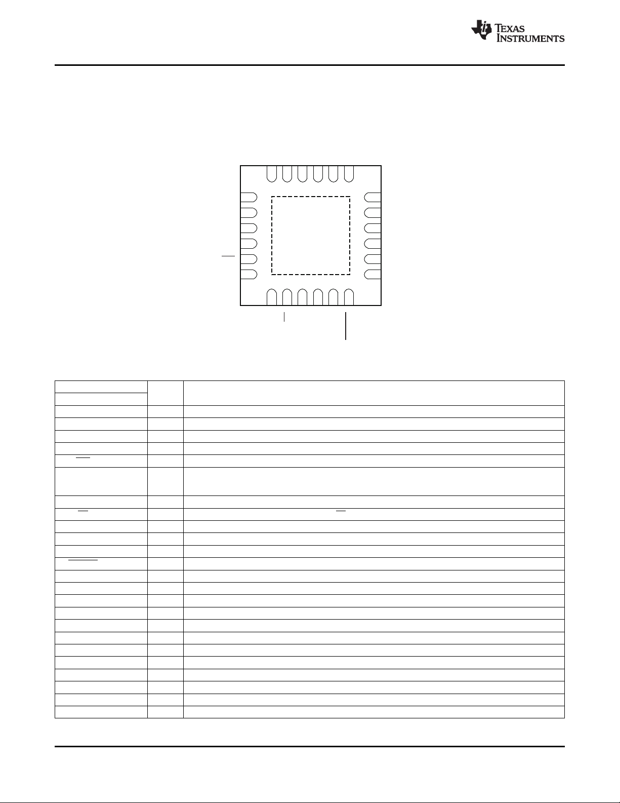
PIN CONFIGURATION
RGE PACKAGE
QFN-24
(TOP VIEW)
PIN DESCRIPTIONS
PIN
NAME NO. I/O DESCRIPTION
IN4 1 I Input channel single-ended 4 or differential pair 3
IN5 2 I Input channel single-ended 5 or differential pair 3
IN6 3 I Input channel single-ended 6 or differential pair 4
IN7 4 I Input channel single-ended 7 or differential pair 4
RST 5 I External hardware reset
BUSY/INT 6 O programmed as an interrupt (INT), this pin is low for a preprogrammed duration after the end of a conversion and valid
SCLK 7 I Serial interface clock
CS 8 I Chip select input for SPI interface slave select (SS)
SDI 9 I Serial data in
SDO 10 O Serial data out
DGND 11 I/O Interface ground
CONVST 12 I Starts conversion
VD 13 I Interface supply
VA 14 I Analog supply (+2.2VDC to +5.5VDC)
REF 15 I External reference input
REFGND 16 I/O Reference ground
PGAOUT 19 O Mux output. Output can be further filtered before sending to ADCIN.
PGAREF 20 I PGA Reference
AGND 17 I/O Analog ground
ADCIN 18 I ADC input
IN0 21 I Analog channel single-ended 0 or differential pair 0
IN1 22 I Analog channel single-ended 1 or differential pair 0
IN2 23 I Analog channel single-ended 2 or differential pair 1
IN3 24 I Analog channel single-ended 3 or differential pair 1
Status output. If programmed as the BUSY pin, this pin is low (default) when a conversion is in progress. If
data are to be output. The polarity of either BUSY or INT is programmable.
4 Submit Documentation Feedback Copyright © 2009–2010, Texas Instruments Incorporated
Product Folder Link(s): ADS8201
ADCDataReadyN
ADCConversionN
2t (SamplingN)
OSC
t (CONVST)
WL
PGA
Settling
ConversionN
ConversionDelay
PGA
Settling
SamplingN+1
N N+1
CONVST
BUSY
INT
ADCState
t (CONVST - sync)
D
t
CD
t (MinimumN+1)
TP
t
CONV
t ( )=40t-CONVST CONVST ,Minimum
D OSC
t
ACQ
ADDataN+1Ready
ADDataNReady
1t
OSC
PGA
Settling
ConversionN
ConversionDelay
Idle
PGA
Settling
ConversionN+1
ConversionDelay
N N+1
RecommendedAD
ReadWindow
ADReadMayCause
ConversionNoise
RecommendedAD
ReadWindow
UpdatingFIFO/ODRN
CONVST
INT
ADCState
SPIPort
22t
OSC
18t +Idle
OSC
t (CS SDO- )
D
t (SCLK - SDOVALID)
D
t (Last SCLK CS- )
SU
t (SDI - )SCLK
H
t (SDI - SCLK)
SU
1 2
3
4
5 6
7
8 9 10
11 12
13 1615
14
D15 D0
D1D2
D3
D4
D5D6
D7
D8D9D10
D11D12
D13
D14
D15 D0
D1D2
D3
D4
D5D6
D7
D8D9D10
D11D12
D13
D14
CS
SDI
SCLK
SDO
t (SCLK - SDOINVALID)
D
t (CS - SDOVALID)
D
t (CS SCLK1- )
SU
t
SH
t
SL
t
SP
ADS8201
www.ti.com
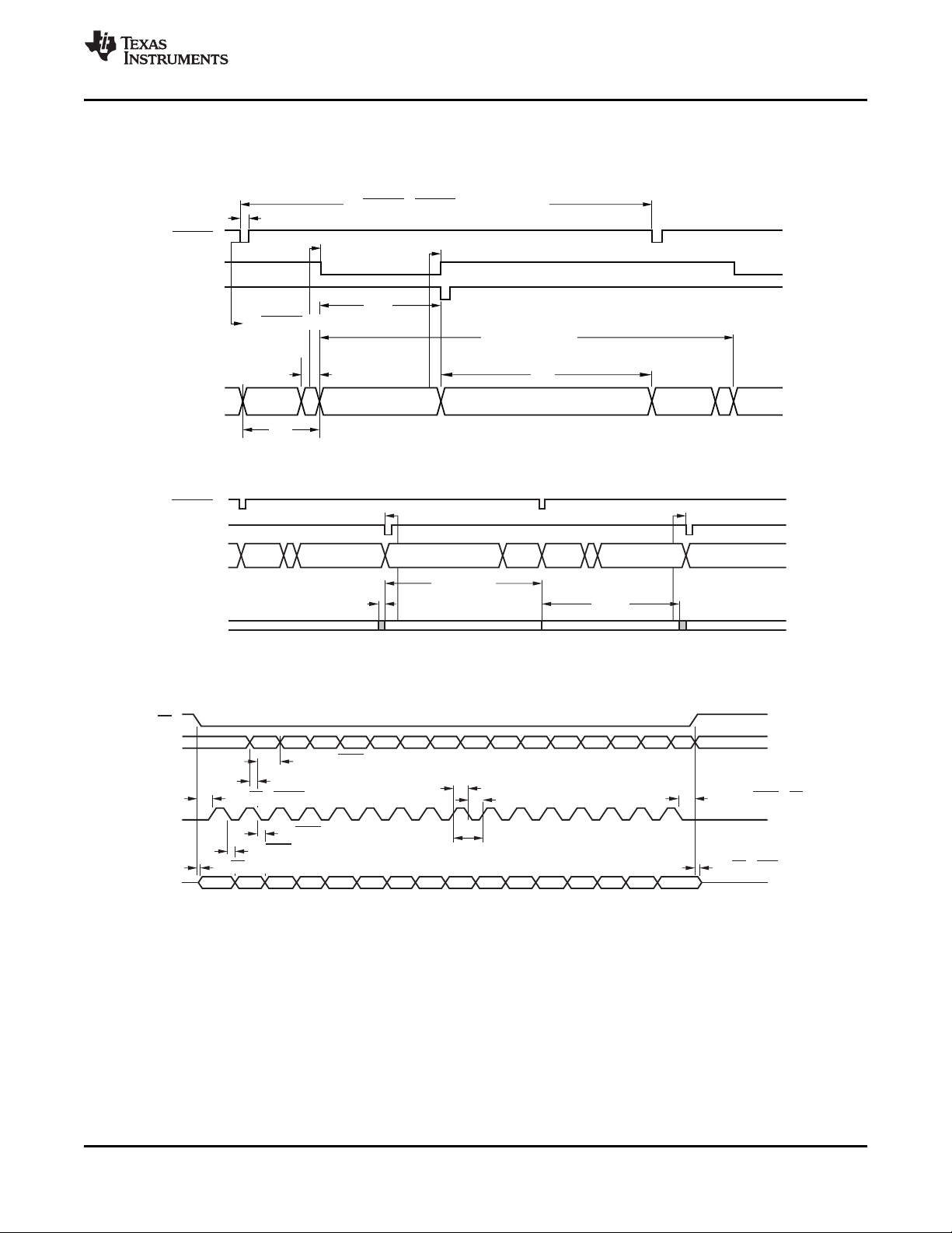
TIMING CHARACTERISTICS
All specifications typical at –40°C to +85°C, 2.2V < VA = V
noted.
Figure 1. Convert Timing
SLAS534B –JULY 2009–REVISED MAY 2010
< 5.5V, and 2.2V < VD < 5.5V, unless otherwise
REF
Figure 2. Read Timing
Figure 3. SPI Convert Timing
Copyright © 2009–2010, Texas Instruments Incorporated Submit Documentation Feedback 5
Product Folder Link(s): ADS8201
AGND
REF-
+IN[0:7]
PGAREF
PGAOUT ADCIN REF+
SDO
CS
SDI
SCLK
CONVST
BUSY/INT
RST
Mux
PGA
G=1/2/4/8
S/H
CDAC
Comparator
SAR
OutputLatches
and
3-State
Drivers
OSC
Conversion
and
ControlLogic
ADS8201
SLAS534B –JULY 2009–REVISED MAY 2010
PARAMETER TEST CONDITIONS MIN TYP MAX UNIT
t
WL
t
OSC
t
H
t
SU
t
D
t
SH
t
SL
t
SP
t
CD
t
ACQ
t
CONV
t
TP
CONVST (Convert Start) pulse width 40 ns
Oscillation time 250 ns
Hold time 2 ns
Setup time 10 ns
Delay time 20 ns
Clock high time 10 ns
Clock low time 10 ns
Clock period 40 ns
Conversion delay time 18 t
Acquisition time 8.5 t
Conversion time 13.5 t
Throughput time 40 t
www.ti.com
TIMING CHARACTERISTICS (continued)
Table 1. Timing Specifications
OSC
OSC
OSC
OSC
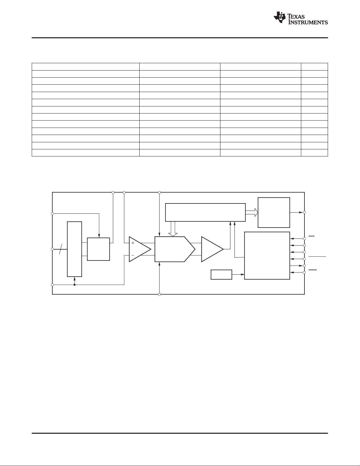
FUNCTIONAL BLOCK DIAGRAM
6 Submit Documentation Feedback Copyright © 2009–2010, Texas Instruments Incorporated
Product Folder Link(s): ADS8201
2
1
0
-1
-2
INL(LSB)
512
0
4096358430722560204815361024
OutputCode
V =5V
DD
V =4.9V
REF
T =+25°C
A
f =100kSPS
SAMPLE
f =4MHz
SCLK
2
1
0
-1
-2
DNL(LSB)
512
0
4096358430722560204815361024
OutputCode
V =5V
DD
V =4.9V
REF
T =+25 C°
A
f =100kSPS
SAMPLE
f =4MHz
SCLK
2
1
0
-1
-2
INL(LSB)
512
0
4096358430722560204815361024
OutputCode
V =2.2V
DD
V
REF
=2.048V
TA=+25°C
f =100kSPS
SAMPLE
f =4MHz
SCLK
2
1
0
-1
-2
DNL(LSB)
512
0
4096358430722560204815361024
OutputCode
V =2.2V
DD
V
REF
=2.048V
TA=+25°C
f =100kSPS
SAMPLE
f =4MHz
SCLK
1200
1000
800
600
400
Power-SupplyCurrent(mA)
-50 -25 0 25 50 75 100 125
Temperature( C)°
V =2.2V,DDV =2.048V
REF
V =5V,DDV =4.9V
REF
2.0
1.8
1.6
1.4
1.2
1.0
0.8
0.6
0.4
0.2
0
Power-DownCurrent(mA)
-50 -25 0 25 50 75 100 125
Temperature(°C)
V =5V,DDV =4.9V
REF
V =2.2V,DDV =2.048V
REF
ADS8201
www.ti.com
SLAS534B –JULY 2009–REVISED MAY 2010
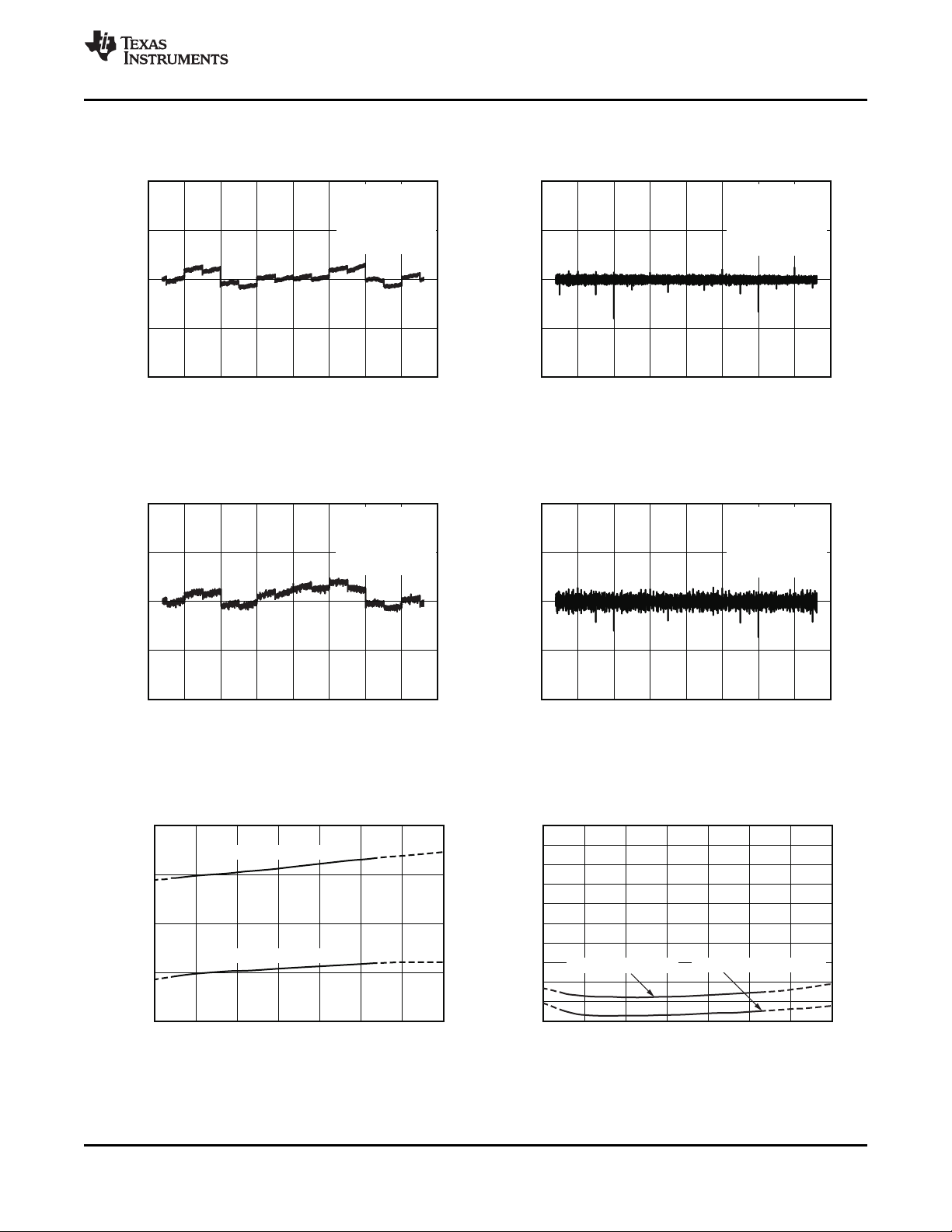
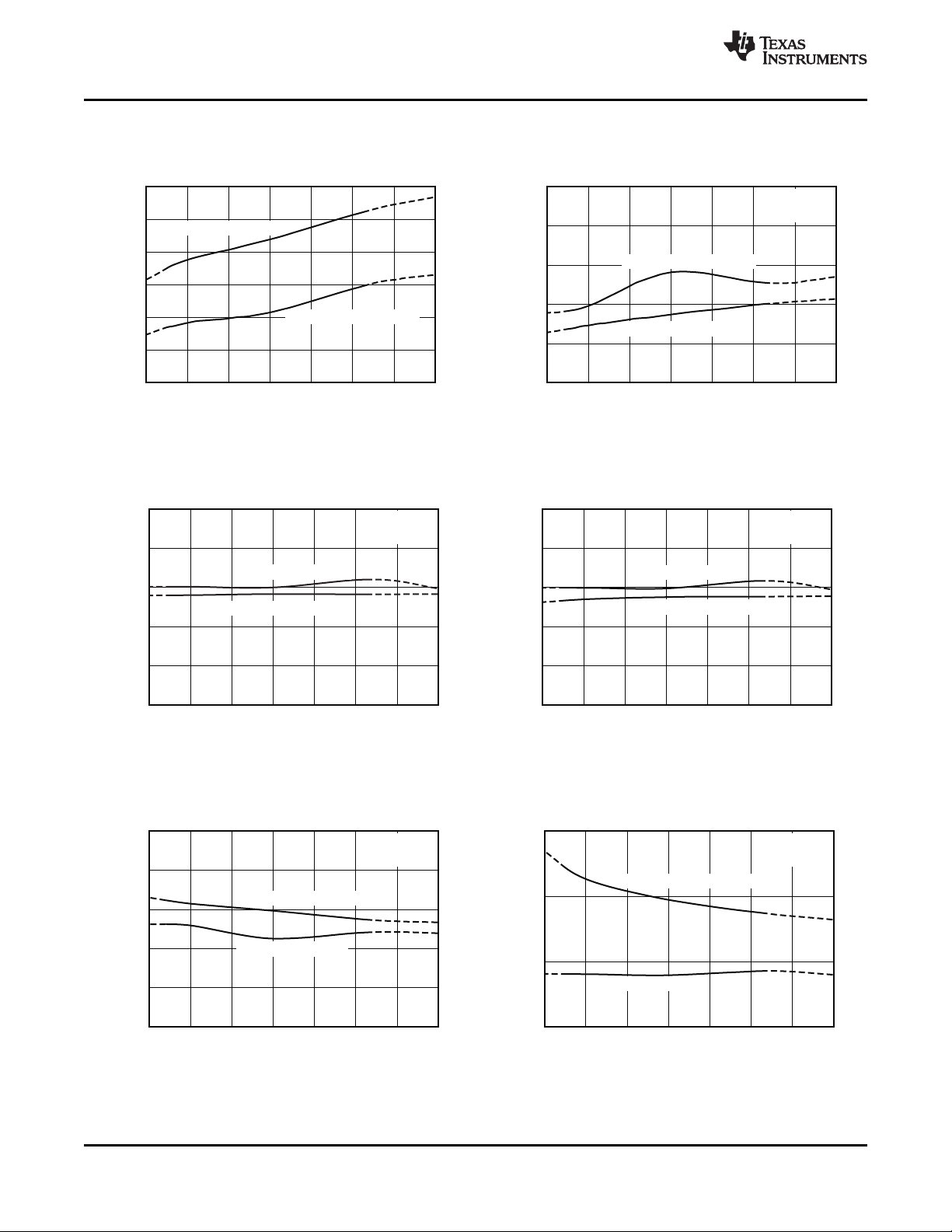
TYPICAL CHARACTERISTICS
LINEARITY ERROR DIFFERENTIAL LINEARITY ERROR
vs CODE vs CODE
Figure 4. Figure 5.
LINEARITY ERROR DIFFERENTIAL LINEARITY ERROR
vs CODE vs CODE
Figure 6. Figure 7.
POWER-SUPPLY CURRENT POWER-DOWN CURRENT
vs TEMPERATURE vs TEMPERATURE
Copyright © 2009–2010, Texas Instruments Incorporated Submit Documentation Feedback 7
Figure 8. Figure 9.
Product Folder Link(s): ADS8201
6
5
4
3
2
1
0
Offset(mV)
-50 -25 0 25 50 75 100 125
Temperature( C)°
V =2.2V,DDV =2.048V
REF
V =5V,DDV =4.9V
REF
-50 -25 0 25 50 75 100 125
Temperature(°C)
0.10
0.08
0.06
0.04
0.02
0
GainError(%)
f =1kHz
IN
f =91kHz
SAMPLE
V =2.2V,DDV =2.048V
REF
V =5V,DDV =4.9V
REF
70
68
66
64
62
60
SNR(dB)
-50 -25 0 25 50 75 100 125
Temperature( C)°
f =1kHz
IN
f =91kHz
SAMPLE
V =2.2V,DDV =2.048V
REF
V =5V,DDV =4.9V
REF
70
68
66
64
62
60
SINAD(dB)
-50 -25 0 25 50 75 100 125
Temperature( C)°
f =1kHz
IN
f =91kHz
SAMPLE
V =2.2V,DDV =2.048V
REF
V =5V,DDV =4.9V
REF
85
82
79
76
73
70
SFDR(dB)
-50 -25 0 25 50 75 100 125
Temperature( C)°
f =1kHz
IN
f =91kHz
SAMPLE
V =2.2V,DDV =2.048V
REF
V =5V,DDV =4.9V
REF
-75
-80
-85
-90
THD(dB)
-50 -25 0 25 50 75 100 125
Temperature( C)°
f =1kHz
IN
f =91kHz
SAMPLE
V =2.2V,DDV =2.048V
REF
V =5V,DDV =4.9V
REF
ADS8201
SLAS534B –JULY 2009–REVISED MAY 2010
SINGLE-ENDED OFFSET VOLTAGE SINGLE-ENDED GAIN ERROR
vs TEMPERATURE vs TEMPERATURE
Figure 10. Figure 11.
SIGNAL-TO-NOISE RATIO SIGNAL-TO-NOISE + DISTORTION
vs TEMPERATURE vs TEMPERATURE
www.ti.com
TYPICAL CHARACTERISTICS (continued)
Figure 12. Figure 13.
SPURIOUS-FREE DYNAMIC RANGE TOTAL HARMONIC DISTORTION
vs TEMPERATURE vs TEMPERATURE
8 Submit Documentation Feedback Copyright © 2009–2010, Texas Instruments Incorporated
Figure 14. Figure 15.
Product Folder Link(s): ADS8201
12
11
10
9
8
7
6
ENOB(dB)
1 2 43 5 7 96 8 10
InputFrequency(kHz)
T =+25A°C
f =91kHz
SAMPLE
V =2.2V,DDV =2.048V
REF
V =5V,DDV =4.9V
REF
80
70
60
50
40
SINAD(dB)
1 2 43 5 7 96 8 10
InputFrequency(kHz)
T =+25 C°
A
f =91kHz
SAMPLE
V =2.2V,DDV =2.048V
REF
V =5V,DDV =4.9V
REF
-60
-70
-80
-90
THD(dB)
1 2 43 5 7 96 8 10
InputFrequency(kHz)
TA=+25°C
f =91kHz
SAMPLE
V =2.2V,DDV =2.048V
REF
V =5V,DDV =4.9V
REF
115
105
95
85
75
Crosstalk(dB)
1 2 43 5 7 96 8 10
InputFrequency(kHz)
T =+25 C°
A
f =91kHz
SAMPLE
V =2.2V,DDV =2.048V
REF
V =5V,DDV =4.9V
REF
4500
4000
3500
3000
2500
2000
1500
1000
500
0
Count
20370203842039502040 2041
4237
2042
109
2043
1
Code
8192Conversions
withV =1.024Vat
IN
2.2VSupply,
V =2.048V,
REF
f =91kHz
SAMPLE
3791
6000
5000
4000
3000
2000
1000
0
Count
208122082
2812
2083
5326
2084522085 2086
0 0
InputFrequency(kHz)
8192Conversionswith
V =2.5Vat5VSupply
IN
V =4.096V
REF
f =91kHz
SAMPLE
ADS8201
www.ti.com
SLAS534B –JULY 2009–REVISED MAY 2010
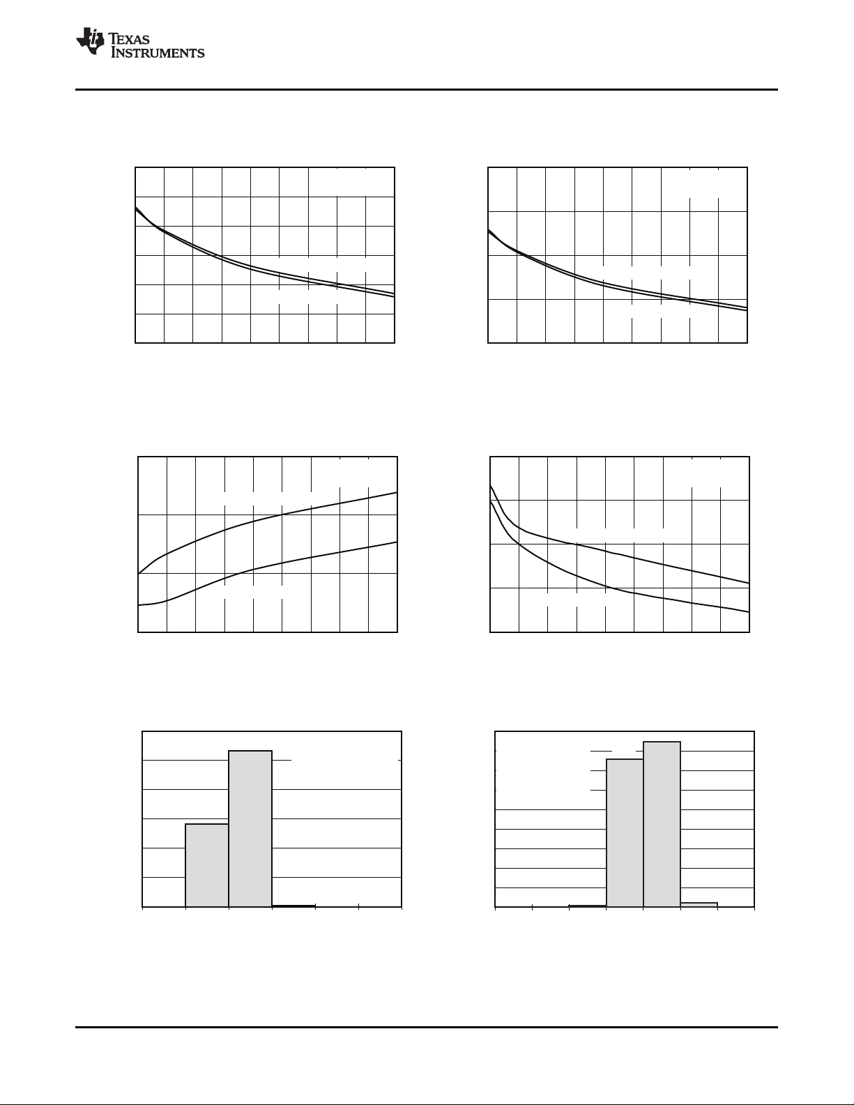
TYPICAL CHARACTERISTICS (continued)
EFFECTIVE NUMBER OF BITS SIGNAL-TO-NOISE + DISTORTION
vs INPUT FREQUENCY vs INPUT FREQUENCY
Figure 16. Figure 17.
TOTAL HARMONIC DISTORTION CROSSTALK
vs INPUT FREQUENCY vs INPUT FREQUENCY
Figure 18. Figure 19.
OUTPUT CODE HISTOGRAM FOR A DC INPUT OUTPUT CODE HISTOGRAM FOR A DC INPUT
Copyright © 2009–2010, Texas Instruments Incorporated Submit Documentation Feedback 9
Figure 20. Figure 21.
Product Folder Link(s): ADS8201

ADS8201
SLAS534B –JULY 2009–REVISED MAY 2010
www.ti.com
THEORY OF OPERATION
The ADS8201 is a low-power data acquisition system that includes a 12-bit successive approximation register
(SAR) analog-to-digital converter (ADC), eight-channel mux, and a first-in first-out (FIFO) buffer. The SAR
architecture is based on charge redistribution, which inherently includes a sample/hold (S/H) function.
The ADS8201 uses an internal clock to run the conversions.
The ADS8201 has eight analog inputs. The analog inputs are either single-ended or differential, depending on
the channel configuration. When a conversion is initiated, the input on these pins is sampled on the internal
capacitor array. While a conversion is in progress, the inputs are disconnected from any internal function. The
device can be programmed for manual channel selection or programmed into an auto-channel select mode that
sweeps through all +INIchannels automatically.
A programmable gain amplifier (PGA) allows for a gain selection of 1, 2, 4, or 8. Individual channels can be
programmed to different gains. This feature allows the ADS8201 to be used in a wide range of applications. The
channel gain mapping feature is very useful in applications where different sensors around different
common-mode voltages must be digitized. Appropriate gain settings can also be chosen to take advantage of the
full range of the converter.
ANALOG INPUT
When the converter enters the hold mode, the voltage on the analog input channel of interest is captured on the
internal capacitor array. The input span is limited to the range of 0.1V to (VA – 0.1V). The PGA front-end
provides a high input impedance that removes the loading effect issues typically associated with high source
impedances.
Care must be taken regarding the absolute analog input voltage. To maintain converter linearity, the +IN and –IN
inputs and the span of [+IN – (–IN)] should be within the limits specified. Exceeding these ranges may cause the
converter linearity to not meet its stated specifications. To minimize noise, use low bandwidth input signals with
low-pass filters.
Care should also be taken to ensure that the output impedance of the sources driving the +IN and –IN inputs are
matched. If this matching is not observed, the two inputs could have different settling times. These different times
may result in offset error, gain error, and linearity error, which all change with temperature and input voltage.
PROGRAMMABLE GAIN AMPLIFIER (PGA)
The ADS8201 features an integrated PGA with gain options of 1, 2, 4, and 8. Each individual channel can be
configured for different gain settings depending on the application. An appropriate gain should be chosen for
each application to take advantage of the full range of the converter.
At power-up, the system settling time is approximately 40ms. This period includes the PGA turn-on time and
settling time to a 12-bit level. Once the device has been configured, the PGA settling time during channel
switching is optimized to provide a throughput of 100k samples-per-second (SPS) in auto-trigger and
auto-channel update modes.
The ADS8201 also provides a PGAOUT pin that can be used for further signal conditioning before inputting to
the ADC. If no additional conditioning is required, the PGAOUT pin should be tied to the ADCIN pin.
BIPOLAR/UNIPOLAR OPERATION
The PGAREF pin allows the ADS8201 to be operated in true differential and bipolar modes. This type of
operation is achieved by setting the PGAREF pin. If this pin is set to GND, the device operates in unipolar mode.
If the PGAREF pin is set to V
differentially ±V
/2. All common-mode signals from 0V to V
REF
configured in differential mode. See the Application Information section for an example of a typical circuit
diagram.
/2, the ADS8201 operates in a bipolar mode. Both +IN and –IN inputs can swing
REF
can be eliminated when the ADS8201 is
REF
10 Submit Documentation Feedback Copyright © 2009–2010, Texas Instruments Incorporated
Product Folder Link(s): ADS8201

ADS8201
www.ti.com
SLAS534B –JULY 2009–REVISED MAY 2010
REFERENCE
The ADS8201 requires an external reference. A clean, low-noise, well-decoupled supply voltage on this pin is
required to ensure good converter performance. A low-noise bandgap reference such as the REF3240 can be
used to drive this pin. A 10mF ceramic decoupling capacitor is required between the REF and REFGND pins of
the converter. These capacitors should be placed as close as possible to the respective device pins. The
REFGND pin should be connected by its own via to the analog ground plane of the printed circuit board (PCB)
with the shortest possible trace. The minimum reference supported by the ADS8201 is 2.048V.
CONVERTER OPERATION
The ADS8201 has an internal clock that controls the conversion rate; the frequency of this clock is 4MHz,
however, this clock can have a variance of up to 20%. The Conversion Delay System Configuration Register
(SCR) at address 0Ah can be used to offset the conversion clock variance. This register allows the conversion
delay to be programmed after conversion from a range of 0.5ms to 15ms. The default conversion delay is set to
4.5ms; however, the appropriate conversion delay can be selected to achieve maximum throughput. Unless the
device is in power-down mode, the internal clock is always on. The minimum acquisition time is 8.5 clock cycles
(this period is equivalent to 2.125ms at 4MHz) after CONVST is asserted. It takes 13.5 conversion clocks
(CCLKs), or approximately 3.375ms, to complete one conversion. The data can be clocked out during the next
4.5ms through the serial interface. Care must be taken to ensure that the next conversion is not initiated until
10ms after the first convert start is asserted.
ADC OPERATING MODE SUMMARY
Table 2 summarizes the ADC operating modes for the ADS8201.
Table 2. ADC Operating Modes
ADC
OPERATING ADC CHANNEL
MODE TRIGGER CONTROL DELAY MUX MULTI-SCAN AUTO PD MODE DESCRIPTION
0 (000) N/A N/A N/A N/A ADC idle
1 (001b) Reserved
2 (010b) Manual Off N/A Off Manual trigger with manual-channel
3 (011b) Manual On N/A Off
4 (100b) Auto trigger Manual On N/A Off Auto trigger with manual-channel
5 (101b) Auto trigger N/A Single scan Off
6 (110b) Auto trigger N/A Multi-scan Off
7 (111b) Reserved
Idle
(no trigger)
Manual
trigger
Manual Manual trigger with manual-channel and
trigger delay mux
Auto Auto trigger with auto-channel and
increment single-scan
Auto Auto trigger with auto-channel and
increment multi-scan
Copyright © 2009–2010, Texas Instruments Incorporated Submit Documentation Feedback 11
Product Folder Link(s): ADS8201
MuxChannelUpdate(Delayed)
MuxChannelUpdate(asHostWrite)
ADCDataReadyN
ADCConversionN
SamplingN
PGA
Settling
ConversionN
ConversionDelay
Idle
PGA
Settling
SamplingN+1
N N+1
CH1 HostWritesCH2
CH1(N+1) CH2(N+2)
CH1(N) CH2(N+1)
CONVST
BUSY
INT
ADCState
ChannelSelectCCR
MuxChannel(Mode2)
MuxChannel(Mode3)
ADS8201
SLAS534B –JULY 2009–REVISED MAY 2010
www.ti.com
MANUAL TRIGGER (See ADC Trigger SCR, Address 08h, Bits[2:0])
Manual-Trigger mode (Modes 2 and 3) can be selected by writing to the ADC Trigger SCR (see the SCR
Register Map). In these modes, it is required to issue a convert start (CONVST) pulse through the CONVST pin
or an ADC read command if bit 0 of the ADC SCR is set to '1' to allow a conversion to initiate through the serial
interface. CCR[0:3] can be used to configure each channel according to the specific application requirements.
For Mode 3, see the Delay Mux Description section for details. Table 3 lists the selection options for manual
channel selection.
Table 3. Manual Channel Selection
SELECTION OPTION BIT SETTINGS
Delay mux select enabled
Delay mux select disabled
(1) See ADC Trigger SCR, bits D[2:0].
(1)
(1)
ADC SCR, bit D[1] = '1'; FIFO buffer enabled (as shown in Figure 22)
ADC SCR, bit D[1] = '0'; FIFO buffer disabled (as shown in Figure 22)
ADC SCR, bit D[1] = '1'; FIFO buffer enabled (as shown in Figure 22)
ADC SCR, bit D[1] = '0'; FIFO buffer disabled (as shown in Figure 22)
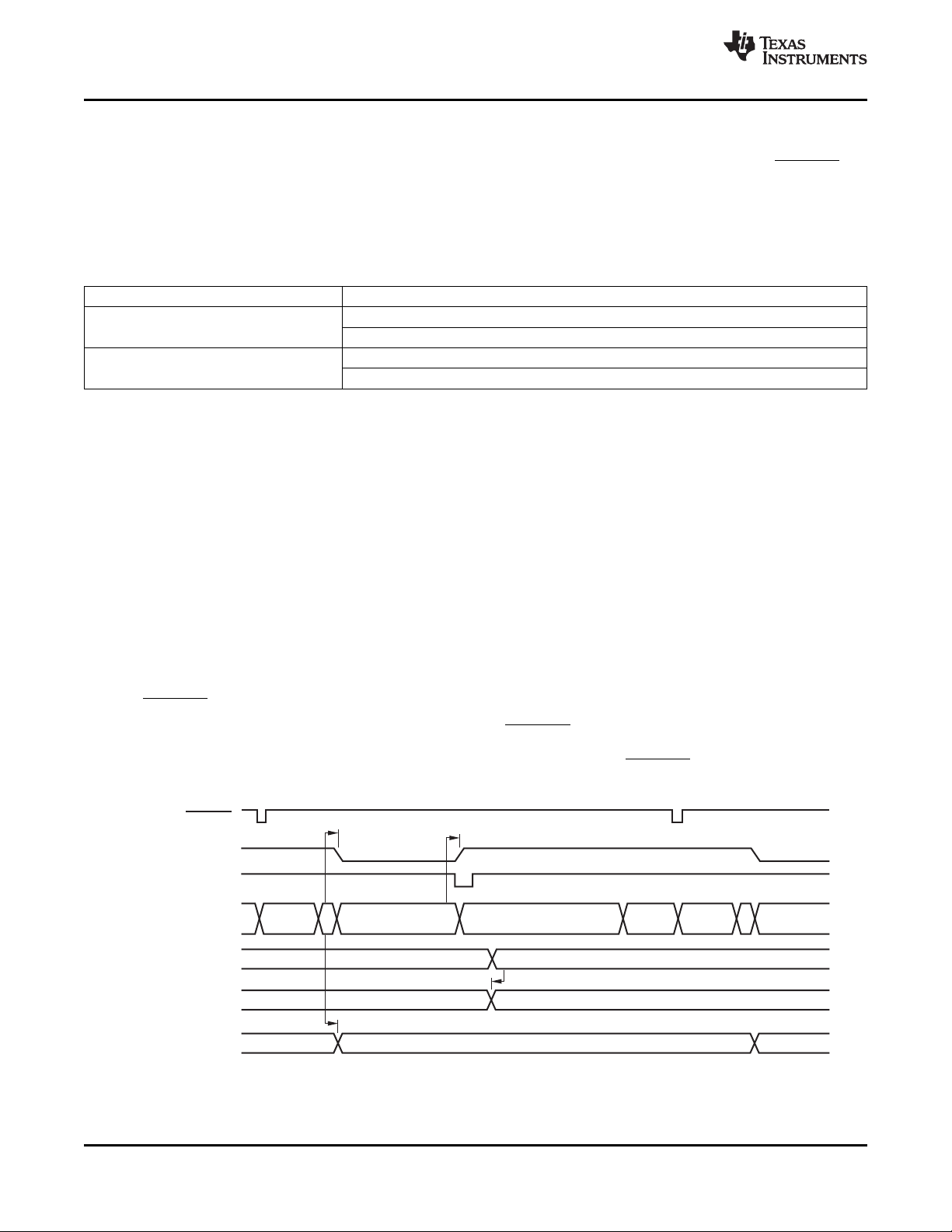
Mode 2 (manual trigger with manual-channel update) provides complete control over the ADS8201 timing. The
user controls when to issue a CONVST and when to read the output data. A switch can be made to any channel
without following any particular sequence. The device can also be configured to enable or disable the FIFO
buffer in this mode.
Mode 3 (manual trigger with manual-channel update and delay mux) allows the ADS8201 to switch the mux to
the next input channel after the current sampling is complete. This capability maximizes the time required for the
PGA to settle for the next channel and subsequently provides faster throughput. See Figure 22 and Figure 25 for
timing details. This increased throughput is the key difference between this mode and Mode 2. The delay mux
feature allows for full 100kSPS throughput, in spite of being in manual trigger and manual channel update mode.
There are two ways to set up the delay mux in this mode. If using the following sequence, then data from first
channel are not repeated:
1. The first channel of interest is set.
2. Mode 3 is selected.
3. The second channel of interest is set.
4. The CONVST pin is asserted.
However, if the second channel of interest is set after the CONVST pin is asserted, then the first conversion
result should be treated as a dummy conversion because the conversion result from the first channel is repeated
twice. Subsequent channels should be selected before asserting the next CONVST in order to achieve the
benefit of the delay mux feature.
(1)
12 Submit Documentation Feedback Copyright © 2009–2010, Texas Instruments Incorporated
Figure 22. Mode 2, Mode 3 Timing
Product Folder Link(s): ADS8201
 Loading...