

Single external op-amp
(optional)
16-bit
ADC
ALERT
SPI
4.096V
+
+
±
AINX Data
HI threshold
LO threshold
MUX
AIN0
AIN1
AIN2
AIN3
AIN4
AIN5
AIN6
AIN7
REFIO
÷2
DVDD
AVDD
Channel
Sequencer
Enhanced-SPI
REFby2
Product
Folder
Order
Now
Technical
Documents
Tools &
Software
Support &
Community
ADS8166,ADS8167,ADS8168
SBAS817C –NOVEMBER 2017–REVISED NOVEMBER 2019
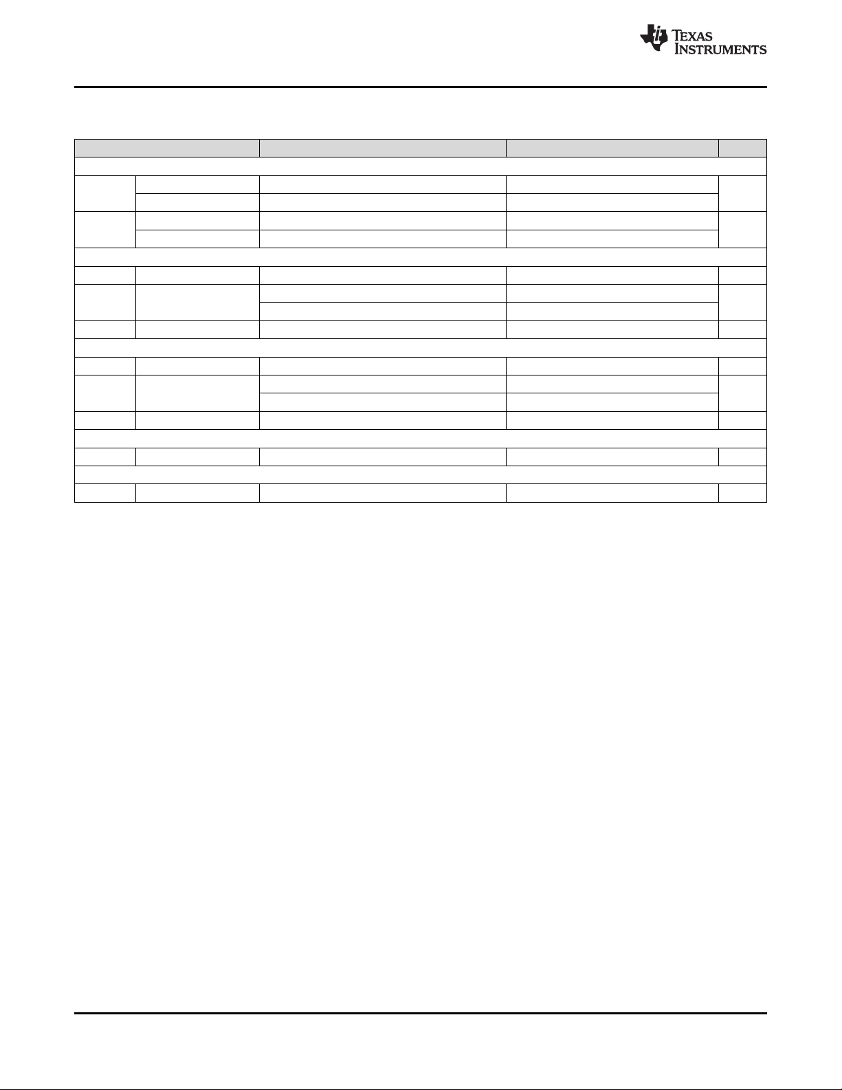
ADS816x 8-Channel, 16-Bit, 1-MSPS, SAR ADC With Direct Sensor Interface
1 Features
1
• Compact low-power data acquisition system:
– MUX breakout enables single external driver
amplifier
– 16-bit SAR ADC
– Low-drift integrated reference and buffer
– 0.5 × V
• Excellent AC and DC performance:
– SNR: 92 dB, THD: –110 dB
– INL: ±0.3 LSB, 16-bit no missing codes
• Multiplexer with channel sequencer:
– Multiple channel-sequencing options:
– Manual mode, on-the-fly mode, auto
sequence mode, custom channel
sequencing
– Early switching enables direct sensor interface
– Fast response time with on-the-fly mode
• System monitoring features:
– Per channel programmable window
comparator
– False trigger avoidance with programmable
hysteresis
• Enhanced-SPI digital interface:
– 1-MSPS throughput with 16-MHz SCLK
– High-speed, 70-MHz digital interface
• Wide operating range:
– External V
– AVDD from 3 V to 5.5 V
– DVDD from 1.65 V to 5.5 V
– –40°C to +125°C temperature range
output for analog input DC biasing
REF
input range: 2.5 V to 5 V
REF
2 Applications
• Analog input modules
• Multiparameter patient monitors
• Anesthesia delivery systems
• LCD tests
• Intra-DC interconnect (metro)
• Optical modules
3 Description
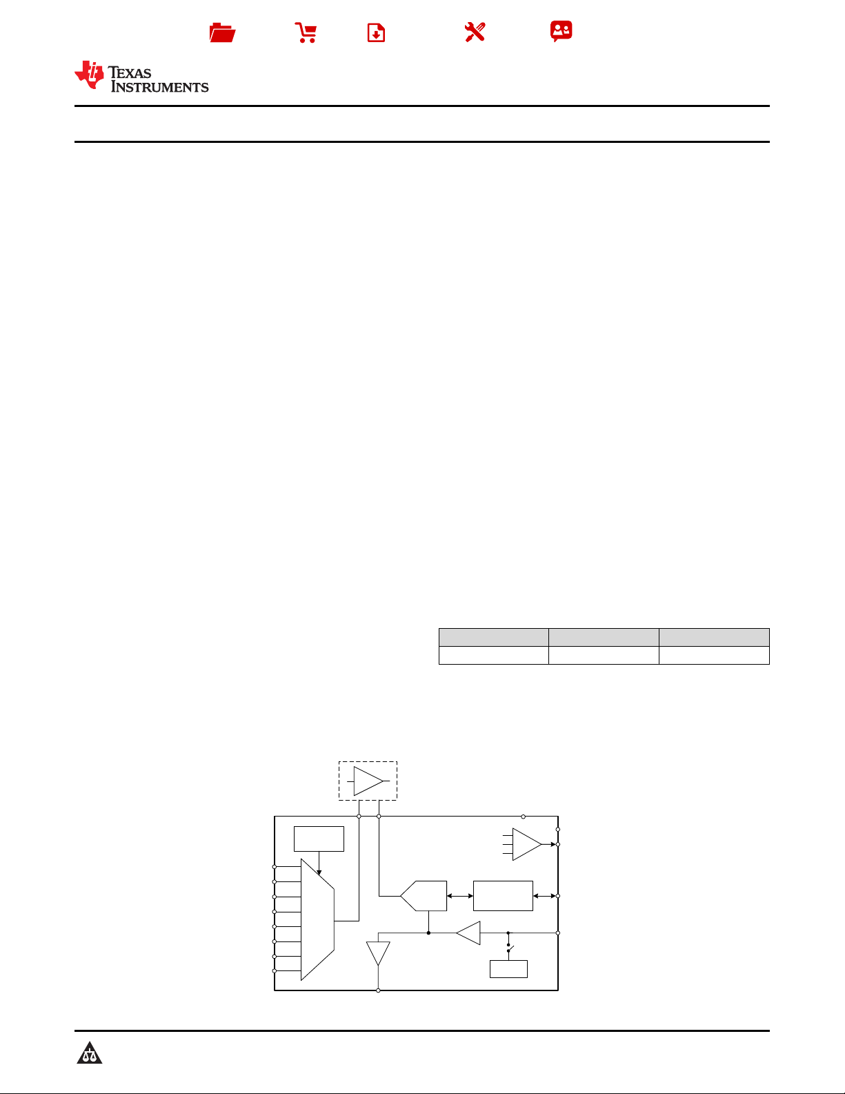
The ADS816x is a family of 16-bit, 8-channel, highprecision successive approximation register (SAR)
analog-to-digital converters (ADCs) operating from a
single 5-V supply with a 1-MSPS (ADS8168),
500-kSPS (ADS8167), and 250-kSPS (ADS8166)
total throughput.
The input multiplexer supports extended settling time,
which makes driving the analog inputs easier. The
output of the multiplexer and ADC analog inputs are
available as device pins. This configuration allows
one ADC driver op amp to be used for all eight
analog inputs of the multiplexer.
The ADS816x features a digital window comparator
with programmable high and low alarm thresholds per
analog input channel. The single op-amp solution with
programmable alarm thresholds enables low power,
low cost, and smallest form-factor applications.
Device Information
PART NUMBER PACKAGE BODY SIZE (NOM)
ADS816x VQFN (32) 5.00 mm × 5.00 mm
(1) For all available packages, see the orderable addendum at
the end of the data sheet.
ADS816x Block Diagram
1
An IMPORTANT NOTICE at the end of this data sheet addresses availability, warranty, changes, use in safety-critical applications,
intellectual property matters and other important disclaimers. PRODUCTION DATA.

ADS8166,ADS8167,ADS8168
SBAS817C –NOVEMBER 2017–REVISED NOVEMBER 2019
www.ti.com
Table of Contents
1 Features.................................................................. 1
2 Applications ........................................................... 1
3 Description ............................................................. 1
4 Revision History..................................................... 2
5 Pin Configuration and Functions......................... 3
6 Specifications......................................................... 5
6.1 Absolute Maximum Ratings...................................... 5
6.2 ESD Ratings.............................................................. 5
6.3 Recommended Operating Conditions....................... 6
6.4 Thermal Information.................................................. 7
6.5 Electrical Characteristics........................................... 8
6.6 Timing Requirements.............................................. 10
6.7 Switching Characteristics........................................ 11
6.8 Typical Characteristics............................................ 14
7 Detailed Description............................................ 19
7.1 Overview................................................................. 19
7.2 Functional Block Diagram....................................... 19
7.3 Feature Description................................................. 20
7.4 Device Functional Modes........................................ 30
7.5 Programming........................................................... 38
7.6 Register Maps......................................................... 44
8 Application and Implementation ........................ 72
8.1 Application Information............................................ 72
8.2 Typical Applications ................................................ 75
9 Power Supply Recommendations...................... 80
10 Layout................................................................... 81
10.1 Layout Guidelines ................................................. 81
10.2 Layout Example .................................................... 83
11 Device and Documentation Support................. 84
11.1 Documentation Support ........................................ 84
11.2 Related Links ........................................................ 84
11.3 Receiving Notification of Documentation Updates 84
11.4 Community Resources.......................................... 84
11.5 Trademarks........................................................... 84
11.6 Electrostatic Discharge Caution............................ 84
11.7 Glossary................................................................ 84
12 Mechanical, Packaging, and Orderable
Information........................................................... 85
4 Revision History
NOTE: Page numbers for previous revisions may differ from page numbers in the current version.
Changes from Revision B (December 2018) to Revision C Page
• Changed document title from ADS816x 8-Channel, 16-Bit, 1-MSPS, SAR ADC With Easy-to-Drive Analog Inputs to
ADS816x 8-Channel, 16-Bit, 1-MSPS, SAR ADC With Direct Sensor Interface.................................................................... 1
• Changed Low-leakage multiplexer with sequencer to Multiplexer with channel sequencer in Features section................... 1
• Changed Wide input range to Wide operating range in Features section, changed and added sub-bullets to this
Features bullet ....................................................................................................................................................................... 1
• Deleted hysteresis from alarm threshold discussion in Description section .......................................................................... 1
• Changed title of ADS816x Block Diagram figure.................................................................................................................... 1
• Changed AUTO_SEQ_CFG1 = 0x84 to AUTO_SEQ_CFG1 = 0x44 in Auto Sequence Mode section .............................. 34
• Changed default settings from 1 to 0xFF in Channel Sample Count column of Custom Channel Sequencing
Configuration Space table .................................................................................................................................................... 36
• Changed reset value from R/W-0000 0001b to R/W-1111 1111b in REPEAT_INDEX_m Registers section ..................... 60
• Changed description of registers 78h, 7Ah, 7Ch, and 7Eh in Digital Window Comparator Configuration Registers
Mapping table ...................................................................................................................................................................... 61
• Changed ALERT_LO_STATUS Register section and name .............................................................................................. 66
• Changed ALERT_STATUS Register section and name ..................................................................................................... 68
• Changed CURR_ALERT_LO_STATUS Register section and name .................................................................................. 69
• Changed CURR_ALERT_STATUS Register section and name ......................................................................................... 71
Changes from Revision A (July 2018) to Revision B Page
• Changed document status from Advanced Information to Production Data .......................................................................... 1
2
Submit Documentation Feedback Copyright © 2017–2019, Texas Instruments Incorporated
Product Folder Links: ADS8166 ADS8167 ADS8168
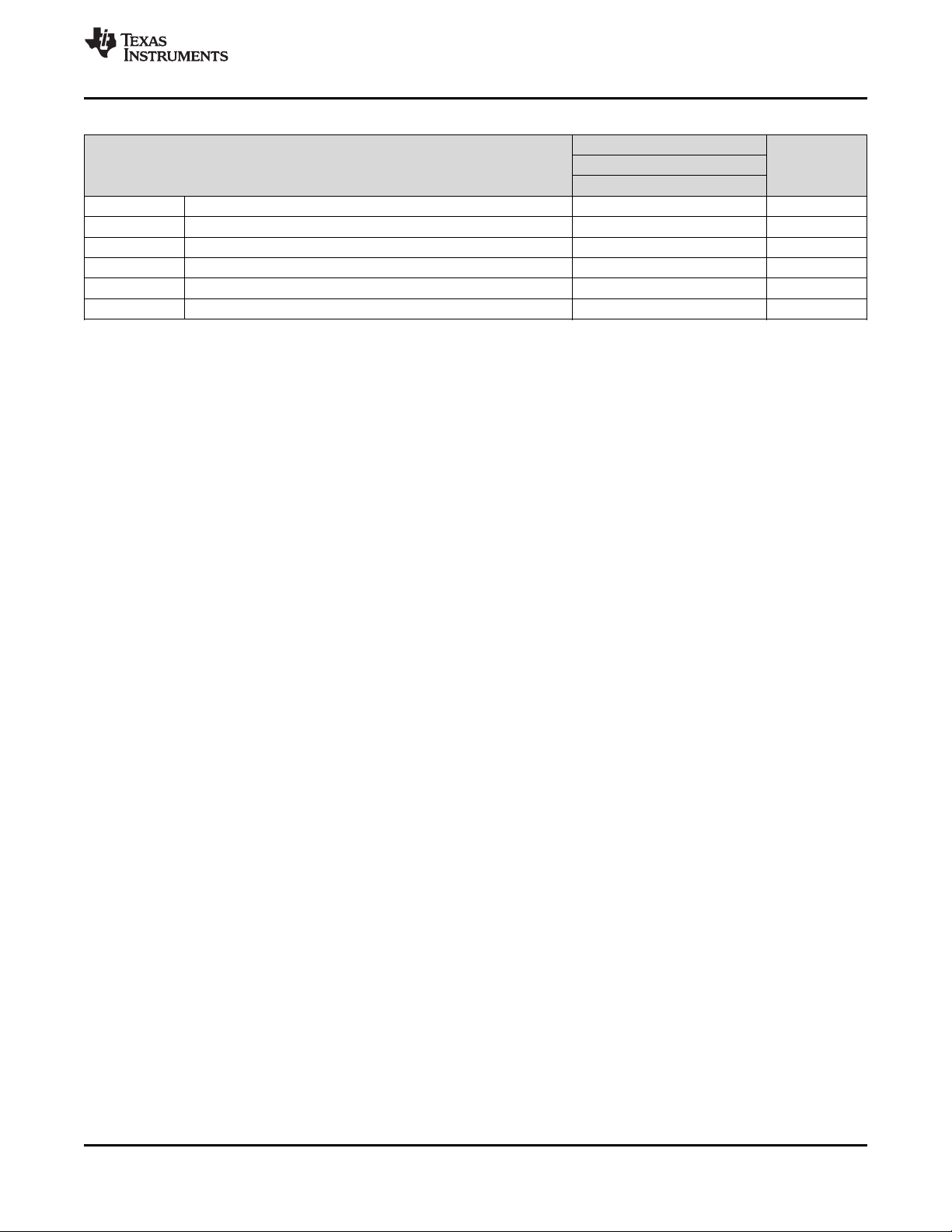
32 AVDD9AIN0
1GND 24 SDI
31 GND10AIN1
2DECAP 23 CS
30 DVDD11AIN2
3REFIO 22 ALERT
29 RST12AIN3
4REFM 21 GND
28 READY13AIN4
5REFP 20 ADC-INM
27 SDO-1/SEQSTS14AIN5
6REFP 19 MUXOUT-M
26 SDO-015AIN6
7REFby2 18 MUXOUT-P
25 SCLK16AIN7
8AIN-COM 17 ADC-INP
Not to scale
Thermal
Pad
www.ti.com
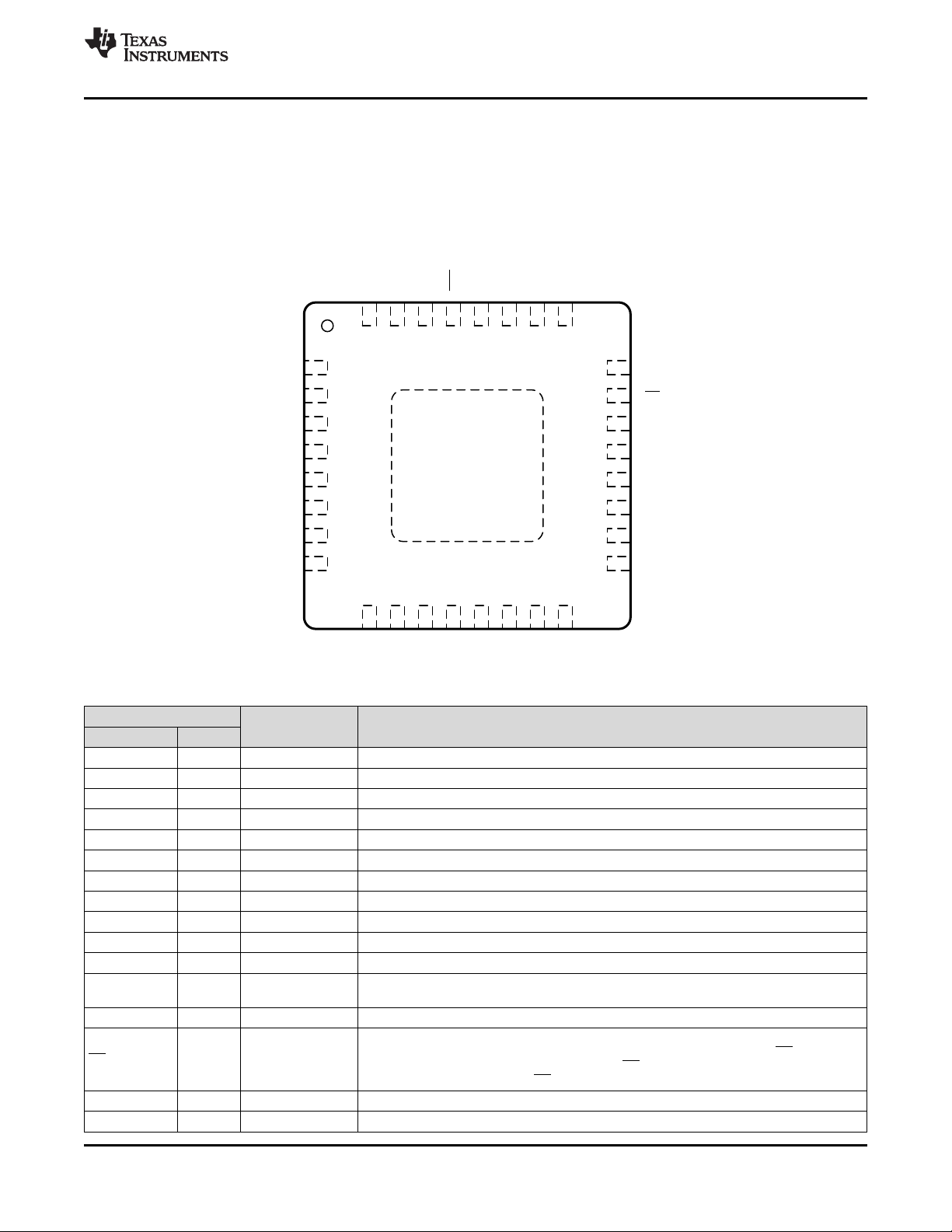
5 Pin Configuration and Functions
ADS8166,ADS8167,ADS8168
SBAS817C –NOVEMBER 2017–REVISED NOVEMBER 2019
RHB Package
32-Pin VQFN
Top View
Pin Functions
PIN
FUNCTION DESCRIPTIONNAME NO.
ADC-INM 20 Analog input Negative ADC analog input
ADC-INP 17 Analog input Positive ADC analog input
AIN0 9 Analog input Analog input channel 0
AIN1 10 Analog input Analog input channel 1
AIN2 11 Analog input Analog input channel 2
AIN3 12 Analog input Analog input channel 3
AIN4 13 Analog input Analog input channel 4
AIN5 14 Analog input Analog input channel 5
AIN6 15 Analog input Analog input channel 6
AIN7 16 Analog input Analog input channel 7
AIN-COM 8 Analog input Common analog input
ALERT 22 Digital output
AVDD 32 Power supply Analog power-supply pin. Connect a 1-µF capacitor from this pin to GND.
CS 23 Digital input
DECAP 2 Power supply Connect a 1-µF capacitor to GND for the internal power supply.
DVDD 30 Power supply Interface power-supply pin. Connect a 1-µF capacitor from this pin to GND.
Digital ALERT output; active high.
This pin is the output of the logical OR of the enabled channel ALERTs.
Chip-select input pin; active low.
The device starts converting the active input channel on the rising edge of CS.
The device takes control of the data bus when CS is low.
The SDO-x pins go Hi-Z when CS is high.
Product Folder Links: ADS8166 ADS8167 ADS8168
Submit Documentation FeedbackCopyright © 2017–2019, Texas Instruments Incorporated
3
ADS8166,ADS8167,ADS8168
SBAS817C –NOVEMBER 2017–REVISED NOVEMBER 2019
Pin Functions (continued)
PIN
FUNCTION DESCRIPTIONNAME NO.
GND 1, 21, 31 Power supply Ground
MUXOUT-M 19 Analog output MUX negative analog output
MUXOUT-P 18 Analog output MUX positive analog output
Multifunction output pin.
READY 28 Digital output
REFby2 7 Analog output
REFIO 3 Analog input/output
REFM 4 Analog input Reference ground potential; short this pin to GND externally.
REFP 5, 6 Analog input/output Reference buffer output, ADC reference input. Short pins 5 and 6 together.
RST 29 Digital input
SCLK 25 Digital input
SDI 24 Digital input
SDO-0 26 Digital output Serial communication pin: data output 0.
SDO-1/
SEQSTS
Thermal pad Supply Exposed thermal pad; connect to GND.
27 Digital output
When CS is held high, READY reflects the device conversion status. READY is low when
a conversion is in process.
When CS is low, the status of READY depends on the output protocol selection.
The output voltage on this pin is equal to half the voltage on the REFP pin.
Connect a 1-µF capacitor from this pin to GND.
Reference voltage input; internal reference is a 4.096-V output.
Connect a 1-µF capacitor from this pin to GND.
Asynchronous reset input pin.
A low pulse on the RST pin resets the device. All register bits return to their default states.
Clock input pin for the serial interface.
All system-synchronous data transfer protocols are timed with respect to the SCLK signal.
Serial data input pin.
This pin is used to transfer data or commands into the device.
Multifunction output pin. By default, this pin indicates the channel scanning status in the
auto and custom channel sequence modes.
In dual SDO data transfer mode this pin functions as a serial communication pin: data
output 1.
www.ti.com
4
Submit Documentation Feedback Copyright © 2017–2019, Texas Instruments Incorporated
Product Folder Links: ADS8166 ADS8167 ADS8168
ADS8166,ADS8167,ADS8168
www.ti.com
SBAS817C –NOVEMBER 2017–REVISED NOVEMBER 2019
6 Specifications
6.1 Absolute Maximum Ratings
over operating ambient temperature range (unless otherwise noted)
AVDD to GND –0.3 7 V
DVDD to GND –0.3 7 V
(2)
AINx
, AIN-COM, MUXOUT-P, MUXOUT-M, ADC-INP, ADC-INM GND – 0.3 AVDD + 0.3 V
REFP REFM – 0.3 AVDD + 0.3 V
REFIO REFM – 0.3 AVDD + 0.3 V
REFM GND – 0.1 GND + 0.1 V
Digital input pins GND – 0.3 DVDD + 0.3 V
Digital output pins GND – 0.3 DVDD + 0.3 V
Input current to any pin except supply pins –10 10 mA
Junction temperature, T
Storage temperature, T
(1) Stresses beyond those listed under Absolute Maximum Rating may cause permanent damage to the device. These are stress ratings
only, which do not imply functional operation of the device at these or any other conditions beyond those indicated under Recommended
Operating Condition. Exposure to absolute-maximum-rated conditions for extended periods may affect device reliability.
(2) AINx refers to AIN0, AIN1, AIN2, AIN3, AIN4, AIN5, AIN6, and AIN7 pins.
J
stg
(1)
MIN MAX UNIT
–40 125 °C
–65 150 °C
6.2 ESD Ratings
Human body model (HBM), per
V
(ESD)
Electrostatic discharge
ANSI/ESDA/JEDEC JS-001, all pins
Charged device model (CDM), per JEDEC
specification JESD22-C101, all pins
(1) JEDEC document JEP155 states that 500-V HBM allows safe manufacturing with a standard ESD control process.
(2) JEDEC document JEP157 states that 250-V CDM allows safe manufacturing with a standard ESD control process.
(1)
(2)
VALUE UNIT
±2000
V
±500
Product Folder Links: ADS8166 ADS8167 ADS8168
Submit Documentation FeedbackCopyright © 2017–2019, Texas Instruments Incorporated
5
ADS8166,ADS8167,ADS8168
SBAS817C –NOVEMBER 2017–REVISED NOVEMBER 2019
www.ti.com
6.3 Recommended Operating Conditions
over operating free-air temperature range (unless otherwise noted)
PARAMETER TEST CONDITIONS MIN TYP MAX UNIT
POWER SUPPLY
AVDD
DVDD
ANALOG INPUTS - SINGLE ENDED CONFIGURATION
FSR Full-scale input range 0 V
V
IN
V
IN
ANALOG INPUTS - PSEUDO-DIFFERENTIAL CONFIGURATION
FSR Full-scale input range –V
V
IN
V
IN
EXTERNAL REFERENCE INPUT
V
REFIO
TEMPERATURE RANGE
T
A
(1) AINx refers to analog inputs AIN0, AIN1, AIN2, AIN3, AIN4, AIN5, AIN6, and AIN7.
(2) CHx_CHy_CFG bits set the analog input configuration as single-ended or pseudo-differential pair. See the AIN_CFG register for more
(3) AINy refers to analog inputs AIN1, AIN3, AIN5, and AIN7 when CHx_CHy_CFG = 01b or 10b. See the Multiplexer
Internal reference 4.5 5 5.5
External reference 3 5 5.5
Operating 1.65 3 5.5
Specified throughput 2.35 3 5.5
Absolute input voltage
(1)
AINx
to REFM and CHx_CHy_CFG
(3)
AINy
to REFM and CHx_CHy_CFG = 01b –0.1 0.1
(2)
= 00b –0.1 V
Absolute input voltage AIN-COM –0.1 0.1 V
/2 V
REF
Absolute input voltage
Absolute input voltage AIN-COM V
AINx to REFM and CHx_CHy_CFG = 00b –0.1 V
AINy to REFM and CHx_CHy_CFG = 10b V
/2 – 0.1 V
REF
/2 – 0.1 V
REF
REFIO input voltage REFIO configured as input pin 2.5 AVDD – 0.3 V
Ambient temperature –40 25 125 °C
details.
Configurations section for more details.
REF
+ 0.1
REF
REF
+ 0.1
REF
/2 + 0.1
REF
/2 + 0.1 V
REF
V
V
V
V
/2 V
V
6
Submit Documentation Feedback Copyright © 2017–2019, Texas Instruments Incorporated
Product Folder Links: ADS8166 ADS8167 ADS8168
ADS8166,ADS8167,ADS8168
www.ti.com
SBAS817C –NOVEMBER 2017–REVISED NOVEMBER 2019
6.4 Thermal Information
ADS816x
THERMAL METRIC
R
θJA
R
θJC(top)
R
θJB
Ψ
JT
Ψ
JB
R
θJC(bot)
Junction-to-ambient thermal resistance 29.5 °C/W
Junction-to-case (top) thermal resistance 18.6 °C/W
Junction-to-board thermal resistance 10.2 °C/W
Junction-to-top characterization parameter 0.2 °C/W
Junction-to-board characterization parameter 10.2 °C/W
Junction-to-case (bottom) thermal resistance 1.3 °C/W
(1) For more information about traditional and new thermal metrics, see the Semiconductor and IC Package Thermal Metrics application
report.
(1)
UNITRHB (VQFN)
32 PINS
Product Folder Links: ADS8166 ADS8167 ADS8168
Submit Documentation FeedbackCopyright © 2017–2019, Texas Instruments Incorporated
7
ADS8166,ADS8167,ADS8168
SBAS817C –NOVEMBER 2017–REVISED NOVEMBER 2019
www.ti.com
6.5 Electrical Characteristics
at AVDD = 5 V, DVDD = 1.65 V to 5.5 V, REFIO configured as output pin, and maximum throughput (unless otherwise
noted); minimum and maximum values at TA= –40°C to +125°C; typical values at TA= 25°C
PARAMETER TEST CONDITIONS MIN TYP MAX UNIT
ANALOG INPUTS
C
SH
C
INMUX
I
LMUX_ON
DC PERFORMANCE
NMC No missing codes 16
INL Integral nonlinearity –0.8 ±0.35 0.8 LSB
DNL Differential nonlinearity –0.5 ±0.2 0.5 LSB
V
OS
dVOS/dT Input offset thermal drift 0.25 µV/°C
G
E
dGE/dT Gain error thermal drift Referred to REFIO ±1 ppm/°C
TNS Transition noise VIN= V
AC PERFORMANCE
SINAD Signal-to-noise + distortion fIN= 2 kHz 91.6 93.5 dB
SNR Signal-to-noise-ratio fIN= 2 kHz 91.8 93.6 dB
THD Total harmonic distortion fIN= 2 kHz -110 dB
SFDR Spurious-free dynamic range fIN= 2 kHz 112 dB
REFERENCE BUFFER
V
RO
C
REFP
R
ESR
REFby2 BUFFER
V
REFby2
I
REFby2
C
REFby2
INTERNAL REFERENCE OUTPUT
V
REFIO
dV
REFIO
C
REFIO
EXTERNAL REFERENCE INPUT
I
REFIO
C
REF
SAMPLING DYNAMICS
t
j-RMS
ADC Input capacitance 60 pF
MUX Input capacitance 13 pF
MUX input on-channel leakage
current
REFM < VIN< REFP –750 ±10 750 nA
Resolution 16 Bits
Input offset error –10 ±0.5 10 LSB
Input offset error match –1 ±0.5 1 LSB
Gain error Referred to REFIO –0.06 ±0.002 0.06 %FSR
Gain error match Referred to REFIO –0.005 ±0.0025 0.005 %FSR
/2 0.6 LSB
REF
Isolation crosstalk fIN= 100 kHz -115 dB
Reference buffer offset voltage
VRO= V
25°C
REFP
- V
REFIO
, TA=
–250 250 µV
Decoupling capacitor on REFP 22 µF
External series resistance 0 1.3 Ω
REFby2 output voltage V
/2 V
REFP
DC Sourcing current from
REFby2
Decoupling capacitor on
REFby2
REFIO output voltage
Internal reference temperature
/dT
drift
(1)
TA= 25°C, REFIO configured
as output pin
1 µF
4.091 4.096 4.101 V
4 18 ppm/°C
Decoupling capacitor on REFIO REFIO configured as output 1 µF
REFIO input current REFIO configured as input pin 0.1 1 µA
Internal capacitance on REFIO
pin
REFIO configured as input pin 10 pF
Aperture delay 4 ns
Aperture jitter 2 ps RMS
2 mA
(1) Does not include the variation in voltage resulting from solder effects.
8
Submit Documentation Feedback Copyright © 2017–2019, Texas Instruments Incorporated
Product Folder Links: ADS8166 ADS8167 ADS8168
ADS8166,ADS8167,ADS8168
www.ti.com
SBAS817C –NOVEMBER 2017–REVISED NOVEMBER 2019
Electrical Characteristics (continued)
at AVDD = 5 V, DVDD = 1.65 V to 5.5 V, REFIO configured as output pin, and maximum throughput (unless otherwise
noted); minimum and maximum values at TA= –40°C to +125°C; typical values at TA= 25°C
PARAMETER TEST CONDITIONS MIN TYP MAX UNIT
f
-3-dB(small)
POWER SUPPLY CURRENTS
I
AVDD
I
DVDD
Small-signal bandwidth Measured at ADC inputs 23 MHz
ADS8168, AVDD = 5 V 5.3 6.4
ADS8167, AVDD = 5 V 3.9 5
ADS8166, AVDD = 5 V 3 4.1
Analog supply current
Static, no conversion 2.3
Static, PD_REFBUF = 1 1.6
Static, PD_REF = 1 800 µA
Digital supply current
Static, PD_REFBUF, PD_REF
and PD_REFby2 = 1
DVDD = 3 V, C
no conversion
LOAD
= 10 pF,
180 µA
0.45 µA
mA
Product Folder Links: ADS8166 ADS8167 ADS8168
Submit Documentation FeedbackCopyright © 2017–2019, Texas Instruments Incorporated
9
ADS8166,ADS8167,ADS8168
SBAS817C –NOVEMBER 2017–REVISED NOVEMBER 2019
www.ti.com
6.6 Timing Requirements
at AVDD = 5 V, DVDD = 1.65 V to 5.5 V, and maximum throughput (unless otherwise noted); minimum and maximum values
at TA= –40°C to +125°C; typical values at TA= 25°C
MIN NOM MAX UNIT
CONVERSION CYCLE
ADS8168 1000
f
CYCLE
t
CYCLE
t
wh_CSZ
t
wl_CSZ
t
ACQ
t
qt_ACQ
t
d_CNVCAP
ASYNCHRONOUS RESET AND LOW POWER MODES
t
wl_RST
SPI-COMPATIBLE SERIAL INTERFACE
f
CLK
t
CLK
t
ph_CK
t
pl_CK
t
ph_CSCK
t
su_CKDI
t
ht_CKDI
t
ht_CKCS
SOURCE-SYNCHRONOUS SERIAL INTERFACE
f
CLK
t
CLK
Sampling frequency
kHzADS8167 500
ADS8166 250
ADS8168 1
ADC cycle-time period
ADS8166 4
Pulse duration: CS high 30 ns
Pulse duration: CS low 30 ns
Acquisition time 300 ns
Quite acquisition time 30 ns
Quiet aperture time 20 ns
Pulse duration: RST low 100 ns
2.35 V ≤ DVDD ≤ 5.5 V,
VIH> 0.7 DVDD, VIL< 0.3 DVDD
Serial clock frequency
1.65 V ≤ DVDD < 2.35 V,
VIH≥ 0.8 DVDD, VIL≤ 0.2 DVDD
1.65 V ≤ DVDD < 2.35 V,
VIH≥ 0.9 DVDD, VIL≤ 0.1 DVDD
Serial clock time period 1/f
CLK
SCLK high time 0.45 0.55 t
SCLK low time 0.45 0.55 t
70
20
68
MHz
CLK
CLK
Setup time: CS falling to the first SCLK capture edge 15 ns
Setup time: SDI data valid to the SCLK capture edge 3 ns
Hold time: SCLK capture edge to (previous) data valid on SDI 4 ns
Delay time: last SCLK falling to CS rising 7.5 ns
2.35 V ≤ DVDD ≤ 5.5 V, SDR
Serial clock frequency
(DATA_RATE = 0b)
2.35 V ≤ DVDD ≤ 5.5 V, DDR
(DATA_RATE = 1b)
Serial clock time period 1/f
CLK
70
MHz
35
ns
µsADS8167 2
ns
10
Submit Documentation Feedback Copyright © 2017–2019, Texas Instruments Incorporated
Product Folder Links: ADS8166 ADS8167 ADS8168
ADS8166,ADS8167,ADS8168
www.ti.com
SBAS817C –NOVEMBER 2017–REVISED NOVEMBER 2019
6.7 Switching Characteristics
at AVDD = 5 V, DVDD = 1.65 V to 5.5 V, and maximum throughput (unless otherwise noted); minimum and maximum values
at TA= –40°C to +125°C; typical values at TA= 25°C
PARAMETER TEST CONDITIONS MIN TYP MAX UNIT
CONVERSION CYCLE
ADS8168 660
t
CONV
ASYNCHRONOUS RESET, AND LOW POWER MODES
t
d_RST
t
PU_ADC
t
PU_REFIO
t
PU_REFBUF
t
PU_Device
SPI-COMPATIBLE SERIAL INTERFACE
t
den_CSDO
t
dz_CSDO
t
d_CKDO
t
d_CSRDY_t
SOURCE-SYNCHRONOUS SERIAL INTERFACE (External Clock)
t
d_CKSTR_r
t
d_CKSTR_f
t
off_STRDO_f
t
off_STRDO_r
t
ph_STR
t
pl_STR
Conversion time
nsADS8167 1200
ADS8166 2500
Delay time: RST rising to READY rising 4 ms
Power-up time for converter module Change PD_ADC = 1b to 0b 1 ms
Power-up time for internal reference Change PD_REF = 1b to 0b 5 ms
Power-up time for internal reference
buffer
Change PD_REFBUF = 1b to 0b 10 ms
Power-up time for device 10 ms
Delay time: CS falling to data enable 15 ns
Delay time: CS rising to SDO going to
Hi-Z
Delay time: SCLK launch edge to (next)
data valid on SDO
15 ns
19 ns
Delay time: CS falling to READY falling 15 ns
Delay time: SCLK launch edge to
READY rising
Delay time: SCLK launch edge to
READY falling
Time offset: READY falling to (next) data
valid on SDO
Time offset: READY rising to (next) data
valid on SDO
–2 2 ns
–2 2 ns
Strobe output high time 2.35 V ≤ DVDD ≤ 5.5 V 0.45 0.55 t
Strobe output low time 2.35 V ≤ DVDD ≤ 5.5 V 0.45 0.55 t
23 ns
23 ns
STR
STR
Product Folder Links: ADS8166 ADS8167 ADS8168
Submit Documentation FeedbackCopyright © 2017–2019, Texas Instruments Incorporated
11
READY
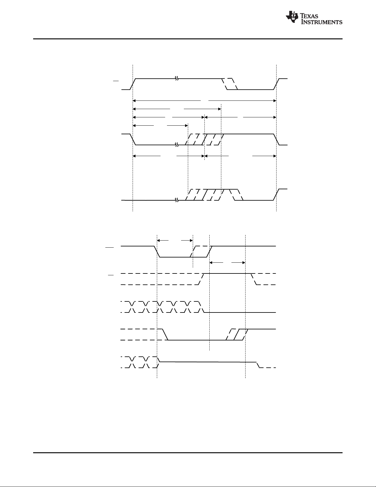
t
wl_RST
SDO-x
RST
CS
SCLK
t
d_rst
ADCST (Internal)
t
cycle
READY
t
conv_min
t
conv_max
CS
t
conv
t
acq
Sample
S
Sample
S + 1
CNV (S) ACQ (S + 1)
ADS8166,ADS8167,ADS8168
SBAS817C –NOVEMBER 2017–REVISED NOVEMBER 2019
www.ti.com
Figure 1. Conversion Cycle Timing
Figure 2. Asynchronous Reset Timing
12
Submit Documentation Feedback Copyright © 2017–2019, Texas Instruments Incorporated
Product Folder Links: ADS8166 ADS8167 ADS8168
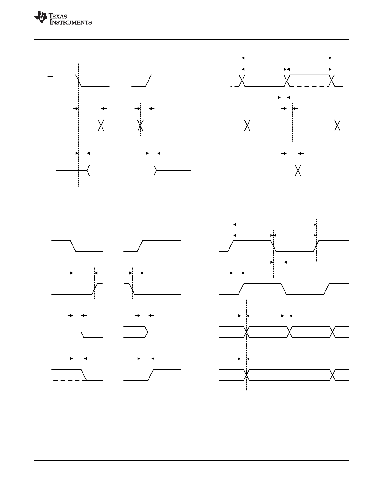
SCLK
SDO-x
CS
t
su_CSCK
t
ht_CKCS
t
den_CSDO
t
dz_CSDO
SCLK
READY
SDO-x
(DDR)
READY
t
d_CSRDY_f
t
d_CSRDY_r
t
ph_CK
t
pl_CK
t
CLK
t
d_CKSTR_r
t
d_CKSTR_f
t
off_STRDO_r
SDO-x
(SDR)
t
off_STRDO_r
t
off_STRDO_f
SCLK
(1)
SDO-x
t
su_CSCK
t
ht_CKCS
t
den_CSDO
t
dz_CSDO
SCLK
(1)
SDI
SDO-x
t
ph_CK
t
pl_CK
t
CLK
t
su_CKDI
t
ht_CKDI
t
d_CKDO
CS
www.ti.com
(1) The SCLK polarity, launch edge, and capture edge depend on the SPI protocol selected.
Figure 3. SPI-Compatible Serial Interface Timing
ADS8166,ADS8167,ADS8168
SBAS817C –NOVEMBER 2017–REVISED NOVEMBER 2019
Figure 4. Source-Synchronous Serial Interface Timing
Product Folder Links: ADS8166 ADS8167 ADS8168
Submit Documentation FeedbackCopyright © 2017–2019, Texas Instruments Incorporated
13
Free-Air Temperature (qC)
Integral Nonlinearity (LSB)
-40 -7 26 59 92 125
-0.5
-0.3
-0.1
0.1
0.3
0.5
D008
Maximum Minimum
Reference Voltage (V)
Differential Nonlinearity (LSB)
2.5 3 3.5 4 4.5 5
-1
-0.6
-0.2
0.2
0.6
1
D050
Maximum
Minimum
Frequency
0
200
400
600
800
1000
1200
1400
1600
1800
-0.6
-0.5
-0.4
-0.3
-0.2
-0.1
0
0.1
0.2
0.3
0.4
0.5
0.6
0 0
6
319
1647
278
0
50
952
1004
223
21
0
ADS8D053
Free-Air Temperature (qC)
Differential Nonlinearity (LSB)
-40 -7 26 59 92 125
-0.3
-0.18
-0.06
0.06
0.18
0.3
D005
Maximum Minimum
ADC Output Code
Differential Nonlinearity (LSB)
0 13107 26214 39321 52428 65535
-0.3
-0.18
-0.06
0.06
0.18
0.3
ADS8ADS8D004
ADC Output Code
Integral Nonlinearity (LSB)
0 13107 26214 39321 52428 65535
-0.5
-0.3
-0.1
0.1
0.3
0.5
D007
ADS8166,ADS8167,ADS8168
SBAS817C –NOVEMBER 2017–REVISED NOVEMBER 2019
www.ti.com
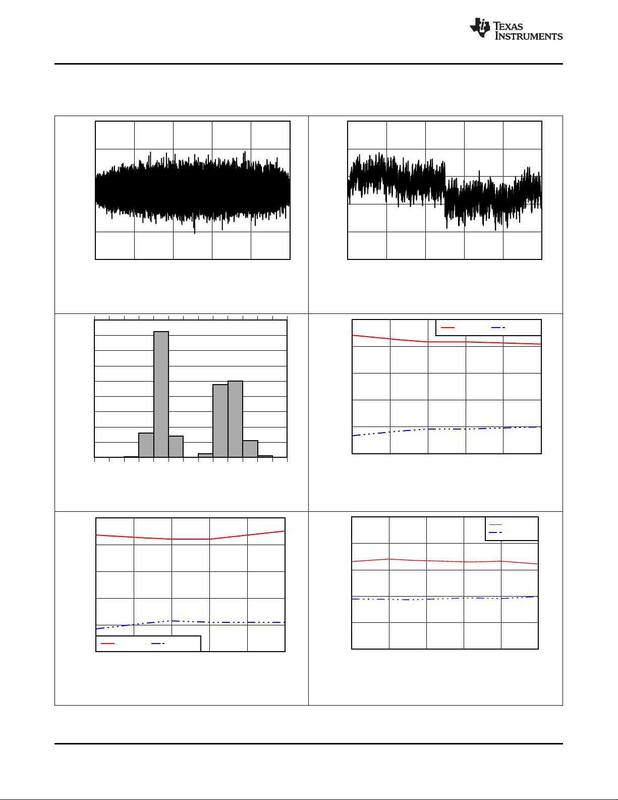
6.8 Typical Characteristics
at AVDD = 5 V, DVDD = 1.65 V to 5.5 V, REFIO configured as output pin, and maximum throughput (unless otherwise noted)
Typical DNL = ±0.15 LSB
Figure 5. Typical DNL
2250 devices
Figure 7. Typical INL Distribution (LSB)
Typical INL = ±0.3 LSB
Figure 6. Typical INL
Figure 8. DNL vs Temperature
14
Submit Documentation Feedback Copyright © 2017–2019, Texas Instruments Incorporated
Figure 9. INL vs Temperature
Product Folder Links: ADS8166 ADS8167 ADS8168
Figure 10. DNL vs Reference Voltage
Reference Voltage (V)
Offset Error (PV)
2.5 3 3.5 4 4.5 5
-50
-40
-30
-20
-10
0
10
20
30
40
50
D011
Free-Air Temperature (qC)
Gain (%FSR)
-40 -7 26 59 92 125
-0.003
-0.002
-0.001
0
0.001
0.002
0.003
0.004
D013
Frequency
0
200
400
600
800
1000
1200
-0.01
-0.005
0
0.0025
0.005
0.0075
0.01
0 0
20
322
1101
722
84
1
0
D055
Temperature (°C)
Offset Error (PV)
-40 -7 26 59 92 125
-50
-40
-30
-20
-10
0
10
D052
Reference Voltage (V)
Integral Nonlinearity (LSB)
2.5 3 3.5 4 4.5 5
-1
-0.6
-0.2
0.2
0.6
1
D051
Maximum
Minimum
Frequency
0
50
100
150
200
250
300
350
400
450
500
550
600
650
700
-1
-0.8
-0.6
-0.4
-0.2
0
0.2
0.4
0.6
0.8
1
0
4
62
249
505
441
209
81
11
0
D054
ADS8166,ADS8167,ADS8168
www.ti.com
SBAS817C –NOVEMBER 2017–REVISED NOVEMBER 2019
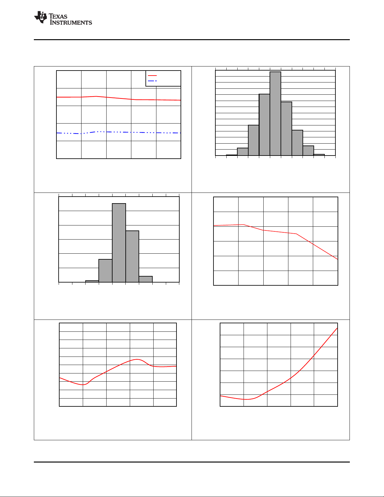
Typical Characteristics (continued)
at AVDD = 5 V, DVDD = 1.65 V to 5.5 V, REFIO configured as output pin, and maximum throughput (unless otherwise noted)
2250 devices
Figure 11. INL vs Reference Voltage
2250 devices
Figure 13. Typical Gain Error Distribution (%FSR)
Figure 12. Typical Offset Distribution (LSB)
REF_SEL[2:0] = 000b
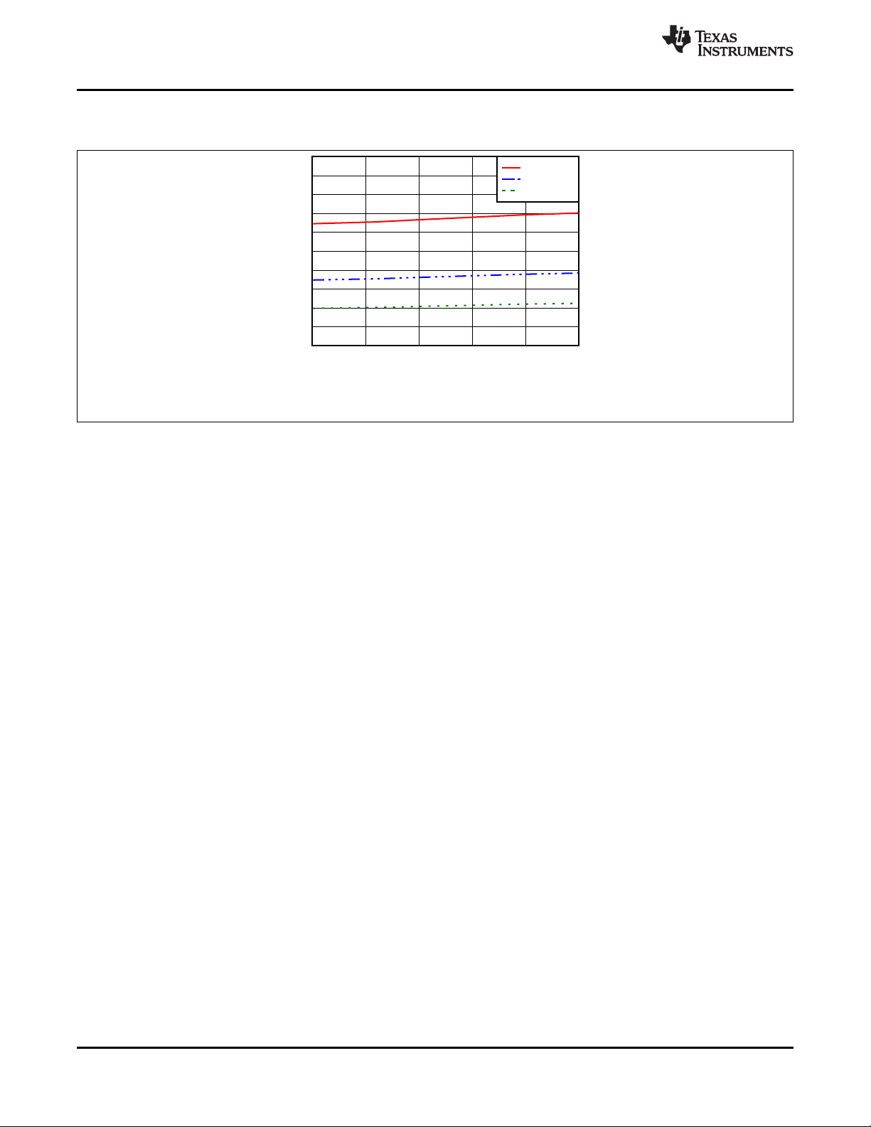
Figure 14. Offset Error vs Temperature
With the appropriate REF_SEL[2:0]; see the OFST_CAL register
Figure 15. Offset Error vs Reference Voltage
Figure 16. Gain Error (ADC + REFBUF) vs Temperature
Product Folder Links: ADS8166 ADS8167 ADS8168
EN_MARG = 0b
Submit Documentation FeedbackCopyright © 2017–2019, Texas Instruments Incorporated
15
fIN, Input Frequency (kHz)
Amplitude (dB)
0 25 50 75 100 125
-200
-160
-120
-80
-40
0
D020
Free-Air Temperature (qC)
SNR, SINAD (dBFS)
ENOB (Bits)
-40 -7 26 59 92 125
92.8 14
93.2 14.4
93.6 14.8
94 15.2
94.4 15.6
94.8 16
D028
SNR
SINAD
ENOB
fIN, Input Frequency (kHz)
Amplitude (dB)
0 100 200 300 400 500
-200
-160
-120
-80
-40
0
D018
fIN, Input Frequency (kHz)
Amplitude (dB)
0 50 100 150 200 250
-200
-160
-120
-80
-40
0
D019
Frequency
0
5000
10000
15000
20000
25000
30000
35000
40000
183
27043
467
D002
Reference Voltage (V)
Gain error (%FSR)
2.5 3 3.5 4 4.5 5
0
0.002
0.004
0.006
0.008
0.01
D014
ADS8166,ADS8167,ADS8168
SBAS817C –NOVEMBER 2017–REVISED NOVEMBER 2019
www.ti.com
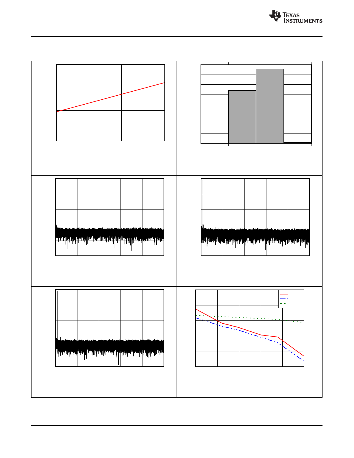
Typical Characteristics (continued)
at AVDD = 5 V, DVDD = 1.65 V to 5.5 V, REFIO configured as output pin, and maximum throughput (unless otherwise noted)
EN_MARG = 0b
Figure 17. Gain Error (ADC + REFBUF) vs Reference Voltage
fIN= 2 kHz, SNR = 93.8 dB, THD = –112.7 dB
Figure 19. Typical FFT, ADS8168
Standard deviation = 0.51 LSB
Figure 18. DC Input Histogram
fIN= 2 kHz, SNR = 93.8 dB, THD = –112.4 dB
Figure 20. Typical FFT, ADS8167
16
fIN= 2 kHz, SNR = 93.8 dB, THD = –111.4 dB
Figure 21. Typical FFT, ADS8166
Submit Documentation Feedback Copyright © 2017–2019, Texas Instruments Incorporated
Figure 22. Noise Performance vs Temperature
Product Folder Links: ADS8166 ADS8167 ADS8168
fIN= 2 kHz
AVDD (V)
I
AVDD (mA)
4.5 4.7 4.9 5.1 5.3 5.5
2
2.5
3
3.5
4
4.5
5
5.5
6
6.5
7
D043
1000 kSPS
500 kSPS
250 kSPS
fIN, Input Frequency (Hz)
THD (dBFS)
SFDR (dBFS)
0 20000 40000 60000 80000 100000
-120 70
-110 80
-100 90
-90 100
-80 110
-70 120
D026
THD
SFDR
Reference Voltage (V)
THD (dBFS)
SFDR (dBFS)
2.5 3 3.5 4 4.5 5
-109.5 116
-110 115
-110.5 114
-111 113
-111.5 112
-112 111
D032
THD
SFDR
fIN, Input Frequency (Hz)
SNR, SINAD (dBFS)
ENOB (Bits)
0 20000 40000 60000 80000 100000
84 13.6
86 14
88 14.4
90 14.8
92 15.2
94 15.6
ADS8ADS8D025
SNR
SINAD
ENOB
Free-Air Temperature (qC)
THD (dBFS)
SFDR (dBFS)
-40 -7 26 59 92 125
-113 106
-112 108
-111 110
-110 112
-109 114
-108 116
-107 118
-106 120
D031
THD
SFDR
Reference Voltage (V)
SNR, SINAD (dBFS)
ENOB (Bits)
2.5 3 3.5 4 4.5 5
90.5 14.7
91 14.8
91.5 14.9
92 15
92.5 15.1
93 15.2
93.5 15.3
94 15.4
94.5 15.5
95 15.6
D029
SNR
SINAD
ENOB
ADS8166,ADS8167,ADS8168
www.ti.com
SBAS817C –NOVEMBER 2017–REVISED NOVEMBER 2019
Typical Characteristics (continued)
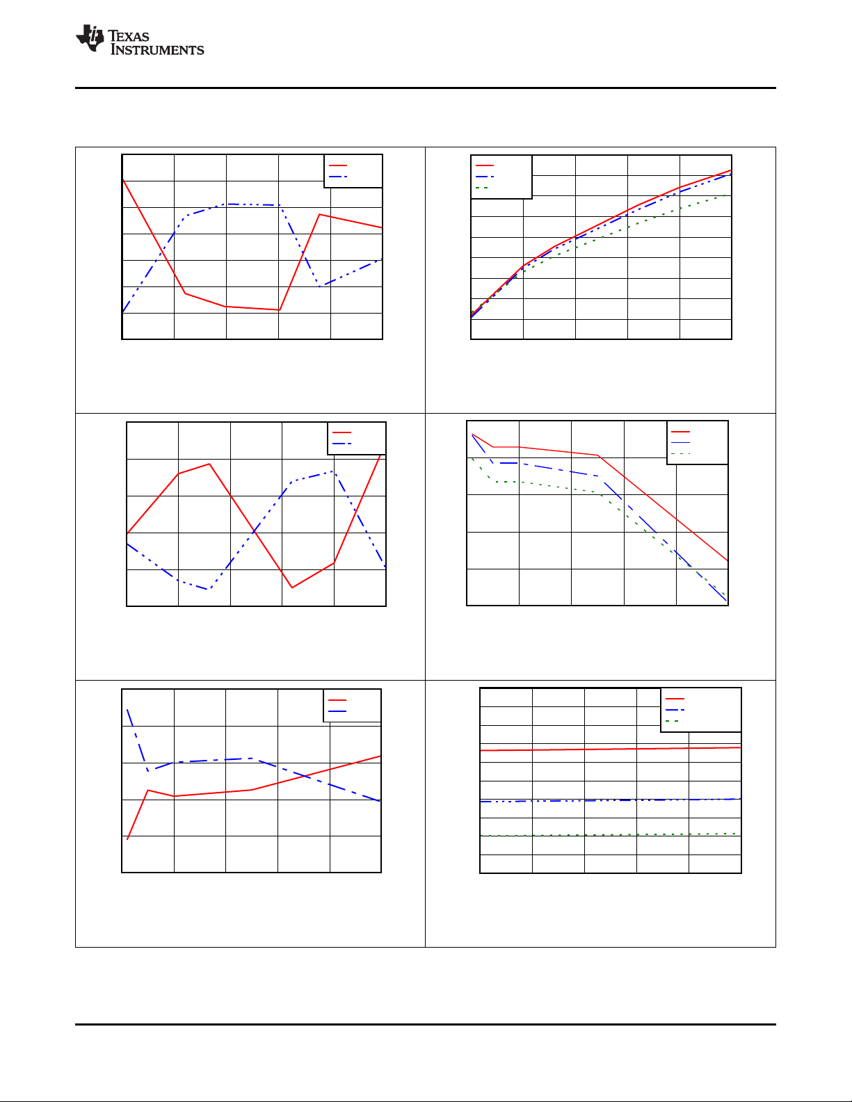
at AVDD = 5 V, DVDD = 1.65 V to 5.5 V, REFIO configured as output pin, and maximum throughput (unless otherwise noted)
fIN= 2 kHz
Figure 23. Distortion Performance vs Temperature
fIN= 2 kHz
Figure 25. Distortion Performance vs Reference Voltage
fIN= 2 kHz
Figure 24. Noise Performance vs Reference Voltage
Figure 26. Noise Performance vs Input Frequency
Figure 27. Distortion Performance vs Input Frequency
Product Folder Links: ADS8166 ADS8167 ADS8168
Figure 28. Analog Supply Current vs Supply Voltage
Submit Documentation FeedbackCopyright © 2017–2019, Texas Instruments Incorporated
17
Free-Air Temperature (qC)
I
AVDD (mA)
-40 -7 26 59 92 125
2
2.5
3
3.5
4
4.5
5
5.5
6
6.5
7
D037
1000 kSPS
500 kSPS
250 kSPS
ADS8166,ADS8167,ADS8168
SBAS817C –NOVEMBER 2017–REVISED NOVEMBER 2019
www.ti.com
Typical Characteristics (continued)
at AVDD = 5 V, DVDD = 1.65 V to 5.5 V, REFIO configured as output pin, and maximum throughput (unless otherwise noted)
AVDD = 5 V
Figure 29. Analog Supply Current vs Temperature
18
Submit Documentation Feedback Copyright © 2017–2019, Texas Instruments Incorporated
Product Folder Links: ADS8166 ADS8167 ADS8168
ADC
4.096-V
÷2
Digital
LDO
AIN0
AIN1
AIN2
AIN3
AIN4
AIN5
AIN6
AIN7
MUXOUT-P ADC-INP AVDD DECAP
MUXOUT-N ADC-INM REFP
REFby2
REFIO
ALERT
READY
SDO-1/SEQSTS
4-WIRE SPI
RST
AIN-COM
Channel
Sequencer
MUX
DVDD
ADS8166,ADS8167,ADS8168
www.ti.com
SBAS817C –NOVEMBER 2017–REVISED NOVEMBER 2019
7 Detailed Description
7.1 Overview
The ADS816x is a 16-bit, successive approximation register (SAR) analog-to-digital converter (ADC) with an
analog multiplexer. This device integrates a reference, reference buffer, REFby2 buffer, low-dropout regulator
(LDO), and features high performance at full throughput and low power consumption.
The ADS816x supports unipolar, single-ended and pseudo-differential analog input signals. The analog
multiplexer is optimized for low distortion and extended settling time. The internal reference generates a low-drift,
4.096-V reference output. The integrated reference buffer supports burst mode for data acquisition of external
reference voltages in the range 2.5 V to 5 V. For DC level shifting of the analog input signals, the device has a
REFby2 output. The REFby2 output is derived from the output of the integrated reference buffer (the REFP pin).
When a conversion is initiated, the differential input between the ADC-INP and ADC-INM pins is sampled on the
internal capacitor array. The device uses an internal clock to perform conversions. During the conversion
process, both analog inputs of the ADC are disconnected from the internal circuit. At the end of conversion
process, the device reconnects the sampling capacitors to the ADC-INP and ADC-INM pins and enters an
acquisition phase.
The integrated LDO allows the device to operate on a single supply, AVDD. The device consumes only
26.5 mW, 19.5 mW, and 15 mW of power when operating at 1 MSPS (ADS8168), 500 kSPS (ADS8167), and
250 kSPS (ADS8166), respectively, with the internal reference, reference buffer, REFby2 buffer, and LDO
enabled.
The enhanced-SPI digital interface is backward-compatible with traditional SPI protocols. Configurable features
boost analog performance and simplify board layout, timing, firmware, and support full throughput at lower clock
speeds. These features enable a variety of microcontrollers, digital signal processors (DSPs), and fieldprogrammable gate arrays (FPGAs) to be used.
The ADS816x enables optical line cards, test and measurement, medical, and industrial applications to achieve
fast, low-noise, low-distortion, and low-power data acquisition in a small form-factor.
7.2 Functional Block Diagram
Product Folder Links: ADS8166 ADS8167 ADS8168
Submit Documentation FeedbackCopyright © 2017–2019, Texas Instruments Incorporated
19
AINx
R
MUX
40
SW
AINy,
AIN-COM
R
MUX
40
SW
C
MUX
13pF
ADC-INP
R
S1
50
SW
C
S1
60pF
ADC-INM
R
S2
50
SW
C
S2
60pF
MUXOUT-M
MUXOUT-P
OR
OR
MUX ADC
AVDD
AVDD
AVDD
AVDD
C
MUX
13pF
ADS8166,ADS8167,ADS8168
SBAS817C –NOVEMBER 2017–REVISED NOVEMBER 2019
www.ti.com
7.3 Feature Description
The ADS816x is comprised of five modules: the converter (SAR ADC), multiplexer (MUX), the reference module,
the enhanced-SPI interface, and the low-dropout regulator (LDO); see the Functional Block Diagram section.
The LDO module is powered by the AVDD supply, and generates the bias voltage for the internal circuit blocks of
the device. The reference buffer drives the capacitive switching load present at the reference pins during the
conversion process. The multiplexer selects among eight analog input channels as the input for the converter
module. The converter module samples and converts the analog input into an equivalent digital output code. The
enhanced-SPI interface module facilitates communication and data transfer between the device and the host
controller.
7.3.1 Analog Multiplexer
Figure 30 shows the small-signal equivalent circuit of the sample-and-hold circuit. Each sampling switch is
represented by resistance (RS1and RS2, typically 50 Ω) in series with an ideal switch (SW). The sampling
capacitors, CS1and CS2, are typically 60 pF.
The multiplexer on-resistance (R
MUXOUT-P or MUXOUT-M pins. The multiplexer analog input typically has a 13-pF on-channel capacitance
(C
).
MUX
), is typically a 40-Ω resistor in series between the ON channel and the
MUX
Figure 30. Input Sampling Stage Equivalent Circuit
During the input signal acquisition phase, the ADC-INP and ADC-INM inputs are individually sampled on CS1and
CS2, respectively. During the conversion process, the device converts for the voltage difference between the two
sampled values: V
Each analog input pin has electrostatic discharge (ESD) protection diodes to AVDD and GND. Keep the analog
inputs within the specified range to avoid turning the diodes on.
20
Submit Documentation Feedback Copyright © 2017–2019, Texas Instruments Incorporated
ADC-INP
– V
.
ADC-INM
Product Folder Links: ADS8166 ADS8167 ADS8168
AIN-COM
AIN0
AIN1
AIN2
AIN3
AIN4
AIN5
AIN6
AIN7
8-channel MUX
Input Pair 1
Input Pair 2
Input Pair 3
Input Pair 4
AIN-COM not used
COM_CFG bit = 0
Configuration - 1 Configuration - 2
Configuration - 3
REFby2
Single-ended
AIN-COM = GND
Pseudo-differential
AIN-COM =
REFby2
AIN-COM
AIN0
AIN1
AIN2
AIN3
AIN4
AIN5
AIN6
AIN7
REFby2
COM_CFG bit = 1
AIN
X
AIN
Y
GND or REFby2
Single-ended
CHx_CHy_CFG = 01b
4-channel MUX
Pseudo-differential
CHx_CHy_CFG = 10b
CHx_CHy_CFG = 00b
Input Pair 1
Input Pair 2
AIN-COM
AIN0
AIN1
AIN2
AIN3
AIN4
AIN5
AIN6
AIN7
REFby2
6-channel MUX
Single-ended
CHx_CHy_CFG = 01b
Pseudo-differential
CHx_CHy_CFG = 10b
AIN
X
AIN
Y
GND or REFby2
4 single inputs
referred to AIN-COM
CHx_CHy_CFG = 00b
Single-ended
AIN-COM = GND
Pseudo-differential
AIN-COM =
REFby2
Channels Input Pairs
Single Inputs
8
7
6
5
0
1
2
3
8
6
4
2
4
4
0
Selectable Channel Configuration
ADS8166,ADS8167,ADS8168
www.ti.com
SBAS817C –NOVEMBER 2017–REVISED NOVEMBER 2019
Feature Description (continued)
7.3.1.1 Multiplexer Configurations
The ADS816x supports single-ended and pseudo-differential analog input signals. The flexible analog input
channel configuration supports interfacing various types of sensors. Figure 31 shows how the analog inputs can
be configured.
Figure 31. Analog Input Configurations
Product Folder Links: ADS8166 ADS8167 ADS8168
Submit Documentation FeedbackCopyright © 2017–2019, Texas Instruments Incorporated
21
ADS8166,ADS8167,ADS8168
SBAS817C –NOVEMBER 2017–REVISED NOVEMBER 2019
www.ti.com
Feature Description (continued)
The analog inputs can be configured as:
• Configuration 1: Eight-channel MUX with the AIN_CFG register set to 00h. The AIN-COM input range is
decided by the COM_CFG register.
– Single-ended inputs with the AIN-COM input set to GND (set the COM_CFG register to 00h).
– Pseudo-differential inputs with the AIN-COM input set to V
• Configuration 2: Four-channel MUX.
– As shown in Table 1, the AIN_CFG register selects the analog input range of individual pairs.
• Configuration 3: Single-ended and pseudo-differential inputs.
– Among the eight analog inputs of the MUX, some inputs can be configured as pairs and some inputs are
configured as individual channels. Table 1 lists options for channel configuration.
– For channels configured as pairs, the AIN_CFG register selects the single-ended or pseudo-differential
configuration for individual pairs.
– For individual channels, the COM_CFG register decides the single-ended or pseudo-differential
configuration.
/ 2 (set the COM_CFG register to 01h).
REF
Table 1. Channel Configuration Options
SERIAL NUMBER TOTAL CHANNELS INPUT PAIRS INDIVIDUAL CHANNELS
1 8 0 8
2 7 1 6
3 6 2 4
4 5 3 2
5 4 4 0
(1) Channel pairs can be formed as [AIN0 - AIN1], [AIN2 - AIN3], [AIN4 - AIN5], and [AIN6 - AIN7].
(2) When channels are configured as pairs, AIN0, AIN2, AIN4, and AIN6 are positive inputs.
(1)(2)
NOTE
The COM_CFG register sets the input voltage range of the AIN-COM pin. AIN-COM pin
must be connected to GND (set the COM_CFG register to 0b) or REFby2 (set the
COM_CFG register to 1b) externally. When using the MUX in a four-channel configuration,
the COM_CFG register has no effect; connect the AIN-COM pin to GND to avoid noise
coupling.
22
Submit Documentation Feedback Copyright © 2017–2019, Texas Instruments Incorporated
Product Folder Links: ADS8166 ADS8167 ADS8168
AINx
R
MUX
40
C
MUX
13pF
AINy,
AIN-COM
R
MUX
40
C
MUX
13pF
ADC-AINP
R
S1
50
C
S1
60pF
ADC-AINM
R
S2
50
C
S2
60pF
MUXOUT-M
MUXOUT-P
MUX
ADC
OR
OR
SW
MUX
SW
MUX
SW
ADC
SW
ADC
CH
X
SW
C
D
MUXOUT
Conventional MUX
C
S
CH
Y
SW
C
D
C
S
CH
X
SW
MUXOUT
ADS816x MUX
C
S
CH
Y
SW
C
S
SW
C
D
SW
C
D
SW
SW
ADS8166,ADS8167,ADS8168
www.ti.com
SBAS817C –NOVEMBER 2017–REVISED NOVEMBER 2019
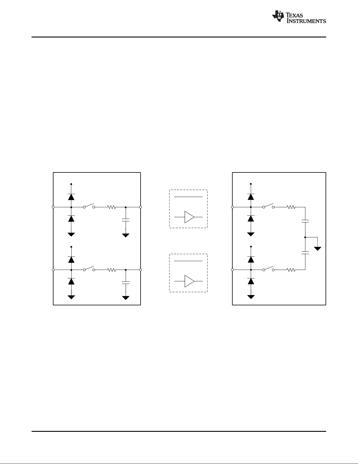
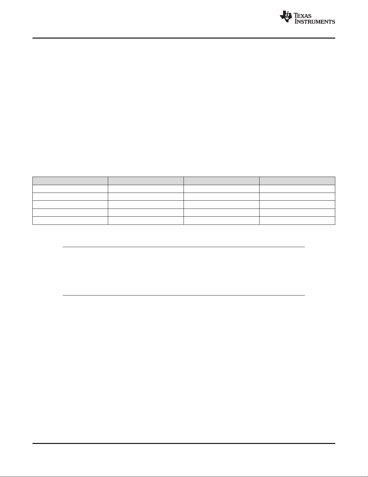
7.3.1.2 Multiplexer With Minimum Crosstalk
For precision measurement in a multichannel system, coupling (such as crosstalk) from one channel to another
can distort the measurement. In conventional multiplexers, as shown in Figure 32, the off channel parasitic
capacitance between the drain and the source of the switch (C
) couples the off channel signal to the on
DSY
channel.
Figure 32 shows that the ADS816x uses a T-switch structure. In this switch architecture, the off channel parasitic
capacitance is connected to ground, which significantly reduces coupling. Care must be taken to avoid signal
coupling on the printed circuit board (PCB), as described in the Layout section.
Figure 32. Isolation Crosstalk in a Conventional MUX versus the ADS816x
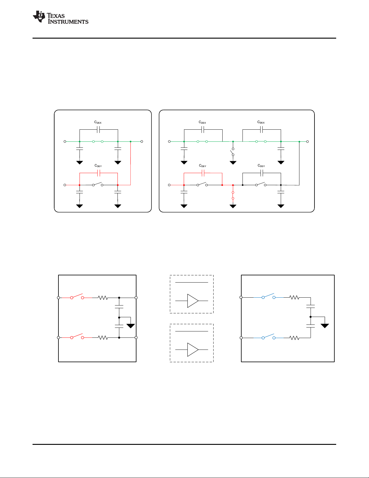
7.3.1.3 Early Switching for Direct Sensor Interface
Figure 33 shows the small-signal equivalent model of the ADS816x analog inputs. The multiplexer input has a
switch resistance (R
) and parasitic capacitance (C
MUX
). The parasitic capacitance causes a charge kickback
MUX
on the MUX analog input at the same time as the ADC sampling capacitor causes a charge kickback on ADC
inputs.
Figure 33. Synchronous and Timed Switching of the MUX and ADC Input Switches
In conventional multichannel SAR ADCs, the acquisition time of the ADC is also the settling time available at the
analog inputs of the multiplexer because these times are internally connected. Thus, high-bandwidth op amps
are required at the analog inputs of the multiplexer to settle the charge kickback. However, multiple highbandwidth op amps significantly increase power dissipation, cost, and size of the solution.
Product Folder Links: ADS8166 ADS8167 ADS8168
Submit Documentation FeedbackCopyright © 2017–2019, Texas Instruments Incorporated
23
SW
ADC
CS
SW
MUX
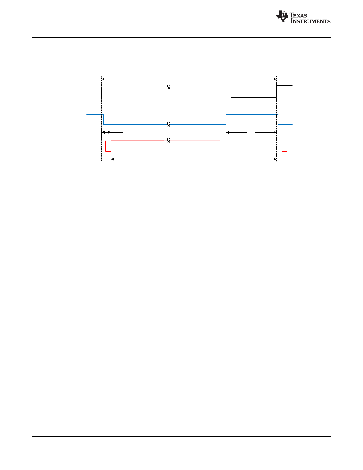
t
CYCLE
CHX Input Settling Time
t
ACQ
100-ns
ADS8166,ADS8167,ADS8168
SBAS817C –NOVEMBER 2017–REVISED NOVEMBER 2019
www.ti.com
The analog inputs of the ADS816x provide a long settling time (t
– 100 ns), resulting in long acquisition time
CYCLE
at the MUX inputs when using a driver amplifier between the MUX outputs and the ADC inputs. Figure 34 shows
a timing diagram of this long acquisition phase. The low parasitic capacitance together with the enhanced settling
time eliminate the need to use an op amp at the multiplexer input in most applications.
Figure 34. Early Switching of the MUX Enables a Long Acquisition Phase
Averaging several output codes of a particular MUX input channel without switching the MUX achieves better
accuracy and noise performance. The output of the multiplexer does not create a charge kickback as long as SDI
is set to 0 (that is, as long as SDI returns the NOP command); see Figure 43 and Figure 45. The multiplexer
does not switch during subsequent conversions except for the first time when a channel is selected. Thus highimpedance sources (such as the voltage from the resistor dividers) can be connected to the analog inputs of the
multiplexer without an op amp.
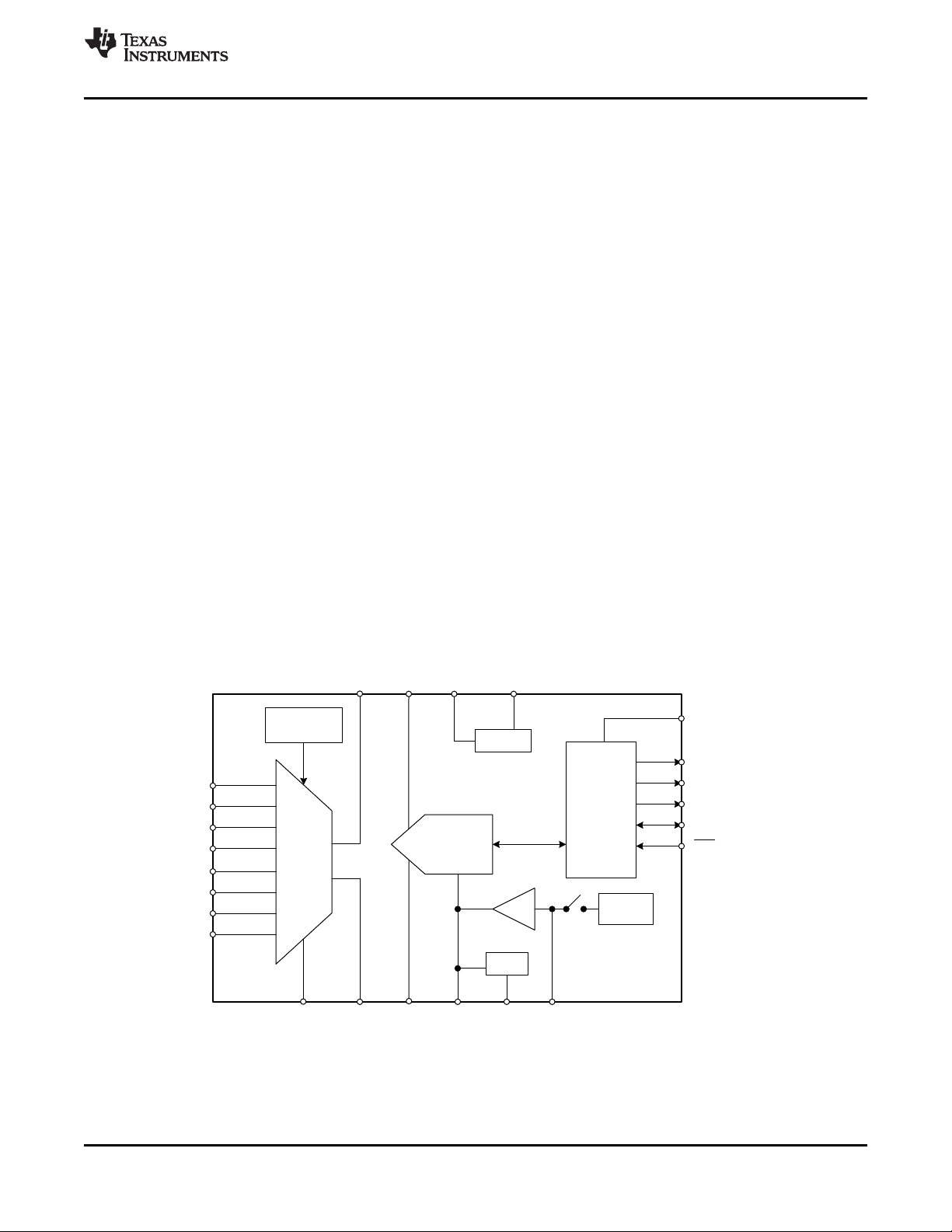
7.3.2 Reference
The ADS816x has a precision, low-drift reference internal to the device. See the Internal Reference section for
details about using the internal reference.
For best SNR performance, the input signal range must be equal to the full-scale input range of the ADC. To
maximize ENOB, an external reference voltage source can be used as described in the External Reference
section.
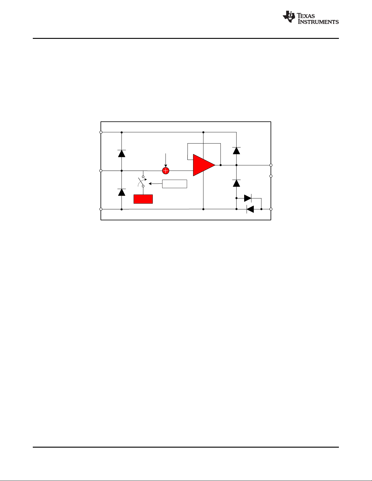
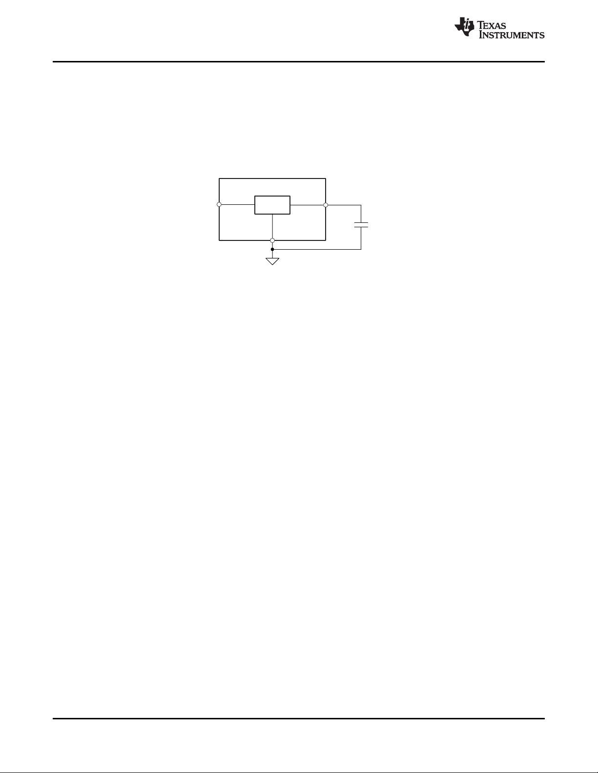
7.3.2.1 Internal Reference
The device features an internal reference source with a nominal output value of 4.096 V. On power-up, the
internal reference is enabled by default. A minimum 1-µF decoupling capacitor, as illustrated in Figure 35, is
recommended to be placed between the REFIO and REFM pins. The capacitor must be placed as close to the
REFIO pin as possible. The output impedance of the internal band-gap circuit creates a low-pass filter with this
capacitor to band-limit the noise of the reference. The internal reference is also temperature compensated to
provide excellent temperature drift over an extended industrial temperature range of –40°C to +125°C. By default
the internal reference is on and the voltage at REFIO is 4.096 V. The REFIO pin has ESD protection diodes to
the AVDD and GND pins.
The initial accuracy specification for the internal reference can be degraded if the die is exposed to any
mechanical or thermal stress. Heating the device when being soldered to a PCB and any subsequent solder
reflow is a primary cause for shifts in the internal reference voltage output. The main cause of thermal hysteresis
is a change in die stress and is therefore a function of the package, die-attach material, and molding compound,
as well as the layout of the device itself.
24
Submit Documentation Feedback Copyright © 2017–2019, Texas Instruments Incorporated
Product Folder Links: ADS8166 ADS8167 ADS8168
ADC
4.096-V
REFP
REFIO
GND
REFM
REF5040
AVDD
OUT
PD_CNTL[3] = 1
(PD_REF)
10 …F 10 …F
1 …F
1-k
AVDD
5-V
ADS816x
ADC
REFP
REFIO
GND
REFM
AVDD
PD_CNTL[3] = 0
(PD_REF)
10 F 10 F
1 F
4.096-V
1-k
ADS816x
5-V
ADS8166,ADS8167,ADS8168
www.ti.com
SBAS817C –NOVEMBER 2017–REVISED NOVEMBER 2019
Figure 35. Device Connections for Using an Internal 4.096-V Reference
7.3.2.2 External Reference
Figure 36 shows the connections for using the device with an external reference. A reference without a low-
impedance output buffer can be used because the input leakage current of the internal reference buffer is less
than 1 µA.
Figure 36. Device Connections for Using an External Reference
7.3.3 Reference Buffer
The ADC starts converting the sampled analog input channel on the CS rising edge and the internal capacitors
are switched to the REFP pins as per the successive approximation algorithm. Most of the switching charge
required during the conversion process is provided by an external decoupling capacitor C
from C
The subsequent conversion occurs with this different reference voltage, and causes a proportional error in the
output code. The internal reference buffer of the device maintains the voltage on the REFP pins within 0.5 LSB of
V
value of C
REFP
. All typical characteristics of the device are specified with the internal reference buffer and the specified
REFP
is not replenished before the next CS rising edge, the voltage on the REFP pins is less than V
.
REFP
Product Folder Links: ADS8166 ADS8167 ADS8168
. If the charge lost
REFP
REFP
Submit Documentation FeedbackCopyright © 2017–2019, Texas Instruments Incorporated
.
25
REFIO
REFM
GND
AVDD
+
±
REFP
REFP
Margin
BUF
ADS816x
4.096-V
PD_REF
ADS8166,ADS8167,ADS8168
SBAS817C –NOVEMBER 2017–REVISED NOVEMBER 2019
www.ti.com
In burst-mode operation, the ADC samples the selected analog input channel for a long duration of time and then
performs a burst of conversions. During the sampling time, the sampling capacitor (CS) is connected to the
differential input pins and no charge is drawn from the REFP pins. However, during the very first conversion
cycle, there is a step change in the current drawn from the REFP pins. This sudden change in load triggers a
transient settling response in the reference buffer. For a fixed input voltage, any transient settling error at the end
of the conversion cycle results in a change in output codes over the subsequent conversions. The internal
reference buffer of the ADS816x, when used with the recommended value of C
, keeps the transient settling
REFP
error at the end of each conversion cycle within 0.5 LSB. Therefore, the device supports burst-mode operation
with every conversion result as per the data sheet specifications.
Figure 37 shows the block diagram of the internal reference and reference buffer.
Figure 37. Internal Reference and Reference Buffer Block Diagram
For the minimum ADC input offset error (VOS), set the REF_SEL[2:0] bits to the value closest to V
OFST_CAL register). The internal reference buffer has a typical gain of 1 V/V with a minimal offset error (V
REF
(see the
(RO)
and the output of the buffer is available between the REFP and the REFM pins. Set the REF_OFST[4:0] (see the
REF_MRG1 register) bits to add or subtract an intentional offset voltage as described in Table 22.
Short the two REFP pins externally. Short the REFM pin to GND externally. Place a decoupling capacitor C
REFP
between the REFP and the REFM pins as close to the device as possible; see Figure 36. See the Layout section
for layout recommendations.
),
26
Submit Documentation Feedback Copyright © 2017–2019, Texas Instruments Incorporated
Product Folder Links: ADS8166 ADS8167 ADS8168
+
-
Ref
Current Sense Amplifier
V
LOAD
Load
V
CC
ADC
REF
ADS816x
REFby2
Configuration 1: High-side / Low-side Current sensing
+
-
AC coupled
sensor
V
CC
ADC
REF
ADS816x
REFby2
Configuration 2: AC Coupled Sensor Interface
+
-
V
CC
ADC
REF
ADS816x
REFby2
Configuration 3:Unity Gain Sensor Interface
+
-
INA
V
CC
ADC
REF
ADS816x
REFby2
Configuration 4: High Impedance Sensor Interface with INA
RR
Ref
V
BRIDGE
INA
R
R
ADS8166,ADS8167,ADS8168
www.ti.com
SBAS817C –NOVEMBER 2017–REVISED NOVEMBER 2019
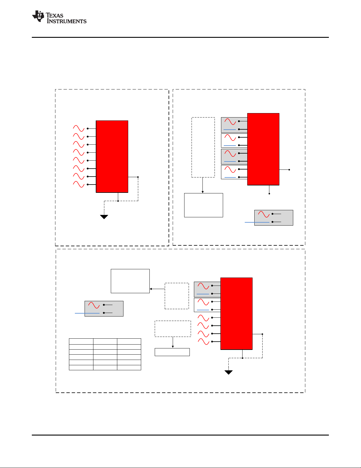
7.3.4 REFby2 Buffer
To use the maximum dynamic range of the ADC, the input signal must be biased around the mid-scale of the
ADC input range. In the ADS816x, where the absolute input range is 0 V to the reference voltage (V
scale is V
/ 2. The REFby2 buffer generates the V
REF
/ 2 signal for mid-scale shifting of the input signal.
REF
REF
), mid-
Figure 38 shows that REFBy2 can be used in various types of sensor signal conditioning circuits.
Figure 38. Signal Conditioning With the REFby2 Buffer
Product Folder Links: ADS8166 ADS8167 ADS8168
Submit Documentation FeedbackCopyright © 2017–2019, Texas Instruments Incorporated
27
GND
AVDD
+
±
REFby2
BUF
ADS816x
REFIO
+
±
BUF
100-k
100-k
ADC
Reference
Margin
REFP
ADS8166,ADS8167,ADS8168
SBAS817C –NOVEMBER 2017–REVISED NOVEMBER 2019
www.ti.com
A resistor divider at the output of the reference buffer, as shown in Figure 39, generates the V
/ 2 signal.
REF
When not using the internal reference buffer (see the PD_CNTL register), any voltage applied at the REFP pin is
applied to the resistor divider. The output of the resistor divider is buffered and available at the REFby2 pin.
Figure 39. REFby2 Buffer Model
The REFby2 buffer is capable of sourcing up to 2 mA of DC current. The REFby2 pin has ESD diode
connections to AVDD and GND.
7.3.5 Converter Module
The converter module samples the analog input signal (provided between the ADC-INP and ADC-INM pins),
compares this signal with the reference voltage (between the REFP pins and REFM pin), and generates an
equivalent digital output code.
The converter module receives the RST and CS inputs from the interface module, and outputs the conversion
result back to the interface module.
7.3.5.1 Internal Oscillator
The device features an internal oscillator (OSC) that provides the conversion clock. Conversion duration varies,
but is bounded by the minimum and maximum value of t
conv
.
28
Submit Documentation Feedback Copyright © 2017–2019, Texas Instruments Incorporated
Product Folder Links: ADS8166 ADS8167 ADS8168
1
FFFF
8000
FSR ± 1 LSBMID-FSR
Analog Input
(AINP AINM)
7FFF
ADC Code (Hex)
V
IN
0
MID ± 1 LSB
-FSR + 1 LSB
ADS8166,ADS8167,ADS8168
www.ti.com
SBAS817C –NOVEMBER 2017–REVISED NOVEMBER 2019
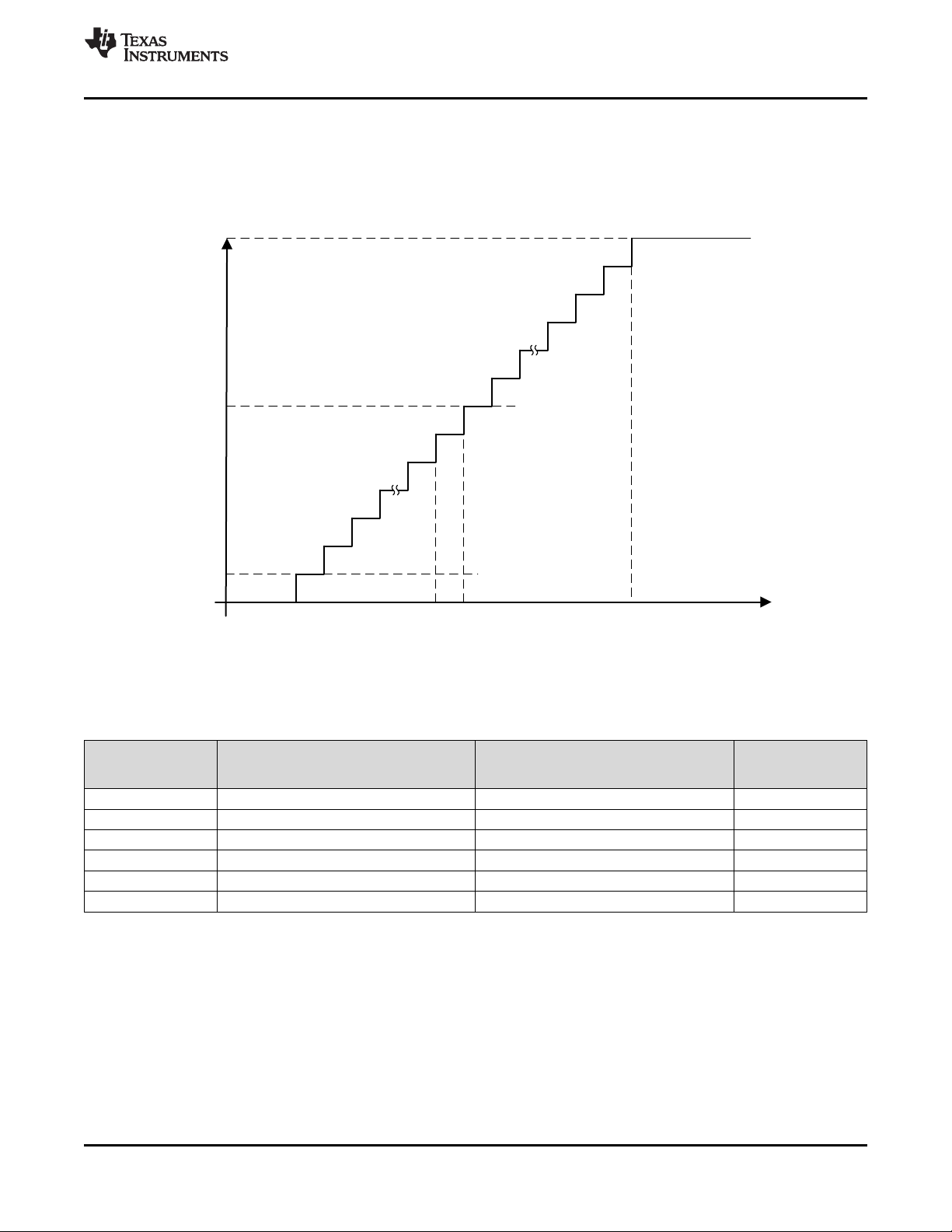
7.3.5.2 ADC Transfer Function
The device supports single-ended and pseudo-differential analog inputs. The device output is in straight binary
format. Figure 40 and Table 2 show the ideal transfer characteristics for a 16-bit ADC with unipolar inputs.
Equation 1 gives the least significant bit (LSB) for the ADC:
1 LSB = V
REF
/ 2
16
(1)
Figure 40. Converter Transfer Characteristics
Table 2. Transfer Characteristics
DESCRIPTION
SINGLE-ENDED INPUT VOLTAGE
(V
= 4.096 V)
REF
FSR – 1 LSB 4.0959375 V 2.0479375 V FFFF
MID + 1 LSB 2.0480625 V 0.0000625 V 8001
MID 2.048 V 0 V 8000
MID – 1 LSB 2.0479375 V –0.0000625 V 7FFF
–FSR + 1 LSB 0.0000625 V –2.0479375 V 0001
–FSR 0 V –2.048 V 0000
PSEUDO-DIFFERENTIAL INPUT
VOLTAGE
(V
= 4.096 V)
REF
OUTPUT CODE
(HEX)
Product Folder Links: ADS8166 ADS8167 ADS8168
Submit Documentation FeedbackCopyright © 2017–2019, Texas Instruments Incorporated
29
LDO
GND
AVDD DECAP
C
LDO
1 F
ADS8166,ADS8167,ADS8168
SBAS817C –NOVEMBER 2017–REVISED NOVEMBER 2019
www.ti.com
7.3.6 Low-Dropout Regulator (LDO)
To enable single-supply operation, the device features an internal low-dropout regulator (LDO). The LDO is
powered by the AVDD supply, and the 2.85-V (nominal) output is available on the DECAP pin. This LDO output
powers the critical analog blocks within the device, and must not be used for any other external purposes.
Decouple the DECAP pin with the GND pin, as shown in Figure 41, by placing a 1-µF, X7R-grade, ceramic
capacitor with a 6.3-V rating from DECAP to GND. There is no upper limit on the value of the decoupling
capacitor; however, a larger decoupling capacitor results in higher power-up time for the device. See the Layout
section for layout recommendations.
Figure 41. Internal LDO Connections
7.4 Device Functional Modes
The multiplexer includes a sequence control logic that supports various features as described in the Channel
Selection Using Internal Multiplexer section.
7.4.1 Channel Selection Using Internal Multiplexer
The ADS816x includes an 8-channel, linear, and low-leakage current analog multiplexer. The multiplexer
performs a break-before-make operation when switching channels. There are four modes of switching the
multiplexer input channels: manual mode, on-the-fly mode, auto sequence mode, and custom channel
sequencing mode.
These modes can be selected by configuring the SEQ_MODE[1:0] bits in the DEVICE_CFG register. On powerup the default mode is manual mode, SEQ_MODE[1:0] = 00b, and the default input channel is AIN0. The
multiplexer configuration registers can be accessed over the SPI; see Figure 50. The SPI interface eliminates the
need for separate MUX control lines.
30
Submit Documentation Feedback Copyright © 2017–2019, Texas Instruments Incorporated
Product Folder Links: ADS8166 ADS8167 ADS8168

t
CONV
CS
Sample
AINx
Sample
AINx
SCLK
Sample
AINy
Sample
AINz
Data AINx Data AINx Data AINy
SDO
24 clocks
MUX OUT = AINx MUX OUT = AINy MUX OUT = AINz
100-ns
t
CYCLE
MUX
Switch to AINy Switch to AINz Switch to AINxSDI
Cycle N Cycle (N + 1) Cycle (N + 2)
ADS8166,ADS8167,ADS8168
www.ti.com
SBAS817C –NOVEMBER 2017–REVISED NOVEMBER 2019
Device Functional Modes (continued)
7.4.1.1 Manual Mode
In manual mode, the channel ID of the desired analog input is configured in the CHANNEL_ID register. On
power-up or after device reset, AIN0 is selected and CHANNEL_ID[2:0] = 000b. Manual mode can be enabled
from any other sequencing mode by programming the SEQ_MODE[1:0] bits to 00b in the DEVICE_CFG register.
Figure 42 shows the timing information for changing channels in manual mode.
The channel information can be updated in a microcontroller (MCU)-friendly 3-byte access. As the 24-bits of
channel configuration are sent over SDI, conversion data are clocked out over SDO. The data on SDO are MSB
aligned and the first 16 clocks correspond to 16 bits of conversion data. The last eight bits of the SDO can be
ignored by the MCU.
As shown in Figure 42, the command to switch to AINy is sent in the Nth cycle and the data corresponding to
channel AINy is available in the (N + 2)th cycle. This switch occurs because the SDI commands are processed
and the ADC starts conversions on the rising edge of CS. Thus, the conversion is processed on the previous
channel (AINx) and not on the updated channel ID (AINy).
Figure 42. Manual Mode Timing Diagram
Product Folder Links: ADS8166 ADS8167 ADS8168
Submit Documentation FeedbackCopyright © 2017–2019, Texas Instruments Incorporated
31

t
CONV
CS
Sample
AINx
Sample
AINy
SCLK
Sample
AINy
Sample
AINy
Data AINx
Data AINy
Data AINy
SDO
24 clocks
MUX OUT = AINx
MUX OUT = AINx
100-ns
t
CYCLE
MUX
Switch to AINySDI
16 clocks
No MUX switching with SDI = 0 (NOP)
Sample
AINy
Data AINy
ADS8166,ADS8167,ADS8168
SBAS817C –NOVEMBER 2017–REVISED NOVEMBER 2019
www.ti.com
Device Functional Modes (continued)
As shown in Figure 43, after selecting AINy the output of the multiplexer does not create a charge kickback as
long as SDI is set to 0 (that is, as long as SDI returns the NOP command). Therefore, high-impedance sources
such as the voltage from resistor dividers can be connected to the analog inputs of the multiplexer without an op
amp.
Figure 43. Manual Mode With No Channel Switching Timing Diagram
7.4.1.2 On-The-Fly Mode
There is a latency of one cycle when switching channels using the register access, just as in manual mode. The
newly selected channel data are available two cycles after selecting the desired channel. The ADS816x supports
on-the-fly switching of the analog input channels of the multiplexer. This mode can be enabled by programming
the SEQ_MODE[1:0] bits to 01b in the DEVICE_CFG register. When enabled, the analog input channel for the
next conversion is determined by the first five bits sent over SDI. The desired analog input channel can be
selected by setting the MSB to 1 and the following four bits as the channel ID. If the MSB is 0 then the SDI
bitstream is decoded as a normal frame on the rising edge of CS. Table 3 lists the channel selection commands
for this mode.
SDI BITS [15:11] SDI BITS [10:0] DESCRIPTION
1 0000 Don't care Select analog input 0
1 0001 Don't care Select analog input 1
1 0010 Don't care Select analog input 2
1 0011 Don't care Select analog input 3
1 0100 Don't care Select analog input 4
1 0101 Don't care Select analog input 5
1 0110 Don't care Select analog input 6
1 0111 Don't care Select analog input 7
1 1000 to 1 1111 Don't care Error bit is set; select analog input 0
Table 3. On-the-Fly Mode Channel Selection Commands
32
Submit Documentation Feedback Copyright © 2017–2019, Texas Instruments Incorporated
Product Folder Links: ADS8166 ADS8167 ADS8168

543
2
241 1
1
t
CONV
CS
Sample
AINx
Sample
AINx
SCLK
Sample
AINy
Sample
AINy
16
Data AINx
SDO
24 clocks
MUX OUT = AINx
MUX OUT = AINy
MUX OUT = AINx
100-ns
t
CYCLE
MUX
Set MODE = 1
4-bit AINy ID
SDI
Data AINy
16 clocks
Data AINx
543
2
1 16
5 clocks
16 clocks
No MUX switching with SDI = 0 (NOP)
543
2
241 1
1
t
CONV
CS
Sample
AINx
Sample
AINx
SCLK
Sample
AINy
Sample
AINz
16
Data AINx
SDO
24 clocks
MUX OUT = AINx
MUX OUT = AINy
MUX OUT = AINx
100-ns
t
CYCLE
MUX
Set MODE = 1
4-bit AINy ID
SDI
1
4-bit AINz ID
Data AINy
16 clocks
Data AINx
543
2
1 16
5 clocks
MUX OUT = AINz
16 clocks
No Cycle Latency
ADS8166,ADS8167,ADS8168
www.ti.com
SBAS817C –NOVEMBER 2017–REVISED NOVEMBER 2019
To set the device in on-the-fly mode, configure EN_ON_THE_FLY to 1b in the ON_THE_FLY_CFG register as
shown in Figure 44 using a 3-byte register access. When in this mode, the 16-bit data transfer can be used to
reduce the required clock speed for operating at full throughput.
Figure 44. On-the-Fly Mode With No MUX Channel Selection Latency
After selecting AINy, as shown in Figure 45, the output of the multiplexer does not create a charge kickback as
long as SDI is set to 0 (that is, as long as SDI returns the NOP command). Thus, high-impedance sources such
as the voltage from resistor dividers can be connected to the analog inputs of the multiplexer without an op amp.
Figure 45. On-the-Fly Mode With No Channel Switching Timing Diagram
Product Folder Links: ADS8166 ADS8167 ADS8168
Submit Documentation FeedbackCopyright © 2017–2019, Texas Instruments Incorporated
33

t
CONV
CS
Sample
AINx
Sample
AINx
SCLK
Sample
AINx
Sample
AIN0
Data AINx Data AINx Data AINx
SDO
24 clocks
MUX OUT = AINx MUX OUT = AIN0
t
CYCLE
MUX
AUTO_SEQ_CH SEQ_STARTSDI
Data AIN0
MUX OUT = AIN1
Data CH
7
MUX OUT = AIN0
SEQSTS
24 clocks 16 c locks
Scan channels AIN0 to AIN7
Sample
AIN0
ADS8166,ADS8167,ADS8168
SBAS817C –NOVEMBER 2017–REVISED NOVEMBER 2019
www.ti.com
7.4.1.3 Auto Sequence Mode
In auto sequence mode, the internal channel sequencer can selectively scan channels from AIN0 through AIN7
in ascending order. To select auto sequence mode, configure SEQ_MODE to 10b in the DEVICE_CFG register
using a 3-byte register access. One or more channels among AIN[7:0] can be enabled by configuring the
AUTO_SEQ_CFG1 register. By default all analog input channels are enabled. After enabling the desired
channels, the sequence can be started by setting SEQ_START to 1b. The ADC auto-increments through the
enabled channels after every CS rising edge. When SEQ_START is set to 1b, the SDO-1/SEQSTS pin is at logic
1 as shown in Figure 46 until the last channel conversion frame is complete. After the last enabled channel
conversion is complete, channel AIN0 is selected and SDO-1/SEQSTS is in a high-impedance state.
Figure 46. Starting a Sequence in Auto Sequence Mode
As an example, Figure 47 depicts a timing diagram for when the device is scanning AIN2 and AIN6 in auto
sequence mode. When AIN6 is converted, SDO-1/SEQSTS is Hi-Z and AIN0 is selected as the active channel.
At the end of sequence, if more conversion frames are launched the device returns valid data corresponding to
AIN0.
To use the device in auto sequence mode follow these steps:
• Set the SEQ_MODE[1:0] bits in the DEVICE_CFG register to 10b.
• Configure the AUTO_SEQ_CFG1 register. In Figure 47, AUTO_SEQ_CFG1 = 0x44.
• Set the SEQ_START bits in the SEQ_START register to 1b to start executing the sequence.
34
Submit Documentation Feedback Copyright © 2017–2019, Texas Instruments Incorporated
Product Folder Links: ADS8166 ADS8167 ADS8168

CS
Sample
AINx
SCLK
Sample
AIN2
Sample
AIN6
Data AINx Data AINx Data AIN2
SDO
24 clocks
MUX OUT = AIN6
t
CYCLE
MUX
SEQ_STARTSDI
SEQSTS
16 clocks 16 clocks
Scan channels AIN2 and AIN6 and repeat
Data AIN6
MUX OUT = AIN2
16 clocks
MUX OUT = AINx
Sample
AIN2
Data AIN2
MUX OUT = AIN6
16 clocks
Sample
AIN6
MUX OUT = AIN2
CS
Sample
AINx
SCLK
Sample
AIN2
Sample
AIN6
Data AINx Data AINx Data AIN2
SDO
24 clocks
MUX OUT = AIN6
t
CYCLE
MUX
SEQ_STARTSDI
SEQSTS
16 clocks 16 clocks
Scan channels AIN2 and AIN6
Data AIN6
MUX OUT = AIN0
16 clocks
MUX OUT = AINx
MUX OUT = AIN2
MUX OUT = AIN0
Sample
AIN0
www.ti.com
ADS8166,ADS8167,ADS8168
SBAS817C –NOVEMBER 2017–REVISED NOVEMBER 2019
Figure 47. Example: Scanning Channels 2 and 6 in Auto Sequence Mode
To repeat a channel sequence indefinitely, set the AUTO_REPEAT bit in the AUTO_SEQ_CFG2 register to 1b.
Figure 48 shows that when the AUTO_REPEAT bit is enabled, the MUX scans through the channels enabled in
the AUTO_SEQ_CFG1 register and repeats the sequence after the last channel data are converted.
Figure 48. Example: Scanning Channels 2 and 6 in Auto Sequence Mode With AUTO_REPEAT = 1
Product Folder Links: ADS8166 ADS8167 ADS8168
Submit Documentation FeedbackCopyright © 2017–2019, Texas Instruments Incorporated
35

ADS8166,ADS8167,ADS8168
SBAS817C –NOVEMBER 2017–REVISED NOVEMBER 2019
www.ti.com
Figure 48 provides a timing diagram for when the device is scanning AIN2 and AIN6 in auto sequence mode with
AUTO_REPEAT = 1b. When AIN6 is converted, AIN2 is selected as the active channel and the device continues
scanning through the enabled channels again.
To use the device in auto sequence with the repeat mode enabled follow these steps:
• Set the SEQ_MODE[1:0] bits in the DEVICE_CFG register to 10b.
• Configure the AUTO_SEQ_CFG1 register. In Figure 47, AUTO_SEQ_CFG1 = 0x44.
• Set AUTO_REPEAT to 1b.
• Set the SEQ_START bit in the SEQ_START register to 1b to start executing the sequence.
To terminate an ongoing channel sequence set the SEQ_ABORT bit in the SEQ_ABORT register 1. When
SEQ_ABORT is set, the auto sequence stops and AIN0 is selected as the active input channel.
7.4.1.4 Custom Channel Sequencing Mode
In this mode the internal channel sequencer can selectively scan channels from AIN0 through AIN7 in any order
as defined by a user-programmable lookup table. Table 4 describes the configurability of this lookup table. The
device can be configured in custom channel sequencing mode by programming the SEQ_MODE[1:0] bits to 11b
in the DEVICE_CFG register using a 3-byte register access. Table 4 shows that the channel scanning sequence
is programmed by configuring the channel IDs in the register as space. A channel sample count can also be
programmed and associated with every channel ID. By default the channel sample count is 1, which means the
sequence executes in the order of programmed channel IDs. If the channel sample count is greater than 1 then
the corresponding channel is sampled and converted for a programmed number of times before switching to the
next channel.
Table 4. Custom Channel Sequencing Configuration Space
REGISTER
ADDRESS
0x8C Index 0 : 3-bit channel ID (default = 0) 0x8D Index 0 : 8-bit sample count (default = 0xFF)
0x8E Index 1 : 3-bit channel ID (default = 0) 0x8F Index 1 : 8-bit sample count (default = 0xFF)
0x90 Index 2 : 3-bit channel ID (default = 0) 0x91 Index 2 : 8-bit sample count (default = 0xFF)
0x92 Index 3 : 3-bit channel ID (default = 0) 0x93 Index 3 : 8-bit sample count (default = 0xFF)
0x94 Index 4 : 3-bit channel ID (default = 0) 0x95 Index 4 : 8-bit sample count (default = 0xFF)
0x96 Index 5 : 3-bit channel ID (default = 0) 0x97 Index 5 : 8-bit sample count (default = 0xFF)
0x98 Index 6 : 3-bit channel ID (default = 0) 0x99 Index 6 : 8-bit sample count (default = 0xFF)
0x9A Index 7 : 3-bit channel ID (default = 0) 0x9B Index 7 : 8-bit sample count (default = 0xFF)
0x9C Index 8 : 3-bit channel ID (default = 0) 0x9D Index 8 : 8-bit sample count (default = 0xFF)
0x9E Index 9 : 3-bit channel ID (default = 0) 0x9F Index 9 : 8-bit sample count (default = 0xFF)
0xA0 Index 10 : 3-bit channel ID (default = 0) 0xA1
0xA2 Index 11 : 3-bit channel ID (default = 0) 0xA3
0xA4 Index 12 : 3-bit channel ID (default = 0) 0xA5
0xA6 Index 13 : 3-bit channel ID (default = 0) 0xA7
0xA8 Index 14 : 3-bit channel ID (default = 0) 0xA9
0xAA Index 15: 3-bit channel ID (default = 0) 0xAB
CHANNEL ID[2:0]
REGISTER
ADDRESS
CHANNEL SAMPLE COUNT[7:0]
Index 10 : 8-bit sample count (default =
0xFF)
Index 11 : 8-bit sample count (default =
0xFF)
Index 12 : 8-bit sample count (default =
0xFF)
Index 13: 8-bit sample count (default =
0xFF)
Index 14 : 8-bit sample count (default =
0xFF)
Index 15 : 8-bit sample count (default =
0xFF)
For application-specific scanning requirements, start and stop pointers can be used to define the channel
scanning sequence. The start index can be programmed in the CCS_START_INDEX register and the stop index
can be programmed in the CCS_END_INDEX register. Table 4 shows that the 4-bit index corresponds to the
configuration index. The sequence starts executing from the index programmed in CCS_START_INDEX (default
0) and stop or loop-back from CCS_STOP_INDEX (default 15). The channel scanning sequence can be loopedback to the start index from the stop index by setting the CCS_SEQ_LOOP register to 1b.
36
Submit Documentation Feedback Copyright © 2017–2019, Texas Instruments Incorporated
Product Folder Links: ADS8166 ADS8167 ADS8168

Low
+
Low
High
ADC
V
IN
+
Low Th - Hysteresis
High Th + Hysteresis
ADC Data
AIN0
AIN7
Logical OR of All
Analog Input Alerts
Alert
Latch
AIN0
AIN1
AIN7
ADS8166,ADS8167,ADS8168
www.ti.com
SBAS817C –NOVEMBER 2017–REVISED NOVEMBER 2019
After configuring the channel scanning order, start index, and stop index the scanning can be initiated by setting
the SEQ_START bit to 1b. The ADC scans through the enabled channels after every CS rising edge as defined
by the channel scanning order. When SEQ_START is set to 1b, the SDO-1/SEQSTS pin is pulled high until the
last channel conversion frame is complete, as described in Figure 46. As illustrated in Figure 47, channel AIN0 is
selected and SEQSTS/SDO-1 goes to Hi-Z after the last enabled channel conversion is complete.
As an example, Figure 47 provides a timing diagram for when the channel configuration is set as in Table 5.
When AIN6 is converted, SEQSTS/SDO-1 goes to Hi-Z and AIN0 is selected as the active channel. If more
conversion frames are launched at the end of the sequence, the device returns valid data corresponding to AIN0.
To use the device in easy capture mode follow these steps:
• Set the SEQ_MODE[1:0] bits in the DEVICE_CFG register to 3.
• Configure the channel sequence by setting registers 0x000C to 0x002B.
• Configure the CCS_START_INDEX and the CCS_END_INDEX registers. In Figure 47, CCS_START_INDEX
= 0 and CCS_STOP_INDEX = 1.
• Configure the CCS_SEQ_LOOP register to 1 to indefinitely loop the sequence. In Figure 47, the
CCS_SEQ_LOOP register = 0b.
• Set the SEQ_START register to 1b to start executing the sequence.
Table 5. Custom Channel Sequencing Configuration Example
REGISTER
ADDRESS
0x8C 010b (Channel 2) 0x8D 1
0x8E 110b (Channel 6) 0x8F 1
CHANNEL ID[2:0]
REGISTER
ADDRESS
CHANNEL SAMPLE COUNT[7:0]
7.4.2 Digital Window Comparator
The ADS816x has a programmable digital window comparator for every analog input channel. The integrated
digital window comparator allows the host to not read ADC data over the serial interface for comparison
purposes. In monitoring applications, the ADC can compare channel data with the set thresholds and alert the
system host using the ALERT pin. Furthermore, the digital window comparator does not require software high
and low comparisons and thus saves processing cycles.
Window comparison is achieved by comparing the channel output code with a programmable high and low digital
threshold. As shown in Figure 49, each analog input channel has a programable hysteresis that is applicable to
both the high and low thresholds of the corresponding channel. Thus, low threshold, high threshold, and
hysteresis configurations are available for each analog input channel.
The thresholds and hysteresis can be configured independently for each analog input channel. The ALERT
Figure 49. Digital Window Comparator
output of the device is a logical OR of all enabled alert outputs corresponding to the analog inputs. The window
comparator can be selectively enabled for the analog inputs by configuring the ALERT_CFG register.
Product Folder Links: ADS8166 ADS8167 ADS8168
Submit Documentation FeedbackCopyright © 2017–2019, Texas Instruments Incorporated
37

GNDGND
CS
MOSI
MISO
SCK
CS
SDI
SDO
SCLK
ADS816x
AVDD DVDD
GND
GND
VDD
5-V
MCU
ADS8166,ADS8167,ADS8168
SBAS817C –NOVEMBER 2017–REVISED NOVEMBER 2019
www.ti.com
The alert status of an individual analog input channel can be read from the ALERT_STATUS register. See the
ALERT_HI_STATUS and ALERT_LO_STATUS registers for further information on the high or low threshold
ALERT, respectively. When monitoring only a low threshold, the high threshold can be set to the ADC positive
full-scale code. Similarly, when monitoring only a high threshold, the low threshold can be set to the negative fullscale code.
7.5 Programming
7.5.1 Data Transfer Protocols
7.5.1.1 Enhanced-SPI Interface
The device features an enhanced-SPI interface that allows the host controller to operate at slower SCLK speeds
and still achieve the required cycle time with a faster response time. Figure 50 shows the ADS816x Interface
connections for the minimum number of pins required by the enhanced-SPI interface.
For any data write operation, the host controller can use any of the four legacy, SPI-compatible protocols to
configure the device, as described in the Protocols for Configuring the Device section. See the Register
Read/Write Operation section for details about the register read or write operation.
For reading ADC conversion data or register data from the device, the enhanced-SPI interface module offers the
following options:
• SPI protocol with a single data output line: SDO-0 (see the SPI Protocols With a Single SDO section)
• SPI protocol with dual data output lines: SDO-1 and SDO-0 (see the SPI Protocols With Dual SDO section)
• Clock re-timer data transfer (see the Clock Re-Timer Data Transfer section)
7.5.1.1.1 Protocols for Configuring the Device
As described in Table 6, the host controller can use any of the four SPI protocols (SPI-00, SPI-01, SPI-10, or
SPI-11) to write data into the device.
(1) See the SDI_CNTL register.
(2) See the SDO_CNTL1 register.
38
Figure 50. 4-Wire SPI Interface Connection Diagram
Table 6. SPI Protocols for Configuring the Device
PROTOCOL
SPI-00 Low Rising 00h 00h Figure 51
SPI-01 Low Falling 01h 00h Figure 51
SPI-10 High Falling 02h 00h Figure 52
SPI-11 High Rising 03h 00h Figure 52
Submit Documentation Feedback Copyright © 2017–2019, Texas Instruments Incorporated
SCLK POLARITY
(At the CS Falling
Edge)
SCLK PHASE
(Capture Edge)
Product Folder Links: ADS8166 ADS8167 ADS8168
SDI_MODE[1:0]
BITS
(1)
SDO_MODE[1:0]
BITS
(2)
DIAGRAM

SCLK
SDI
READY
CPOL = 0
CPOL = 1
CS
MSB MSB-1 LSB+1 LSB
SCLK
SDI
READY
CPOL = 0
CPOL = 1
CS
MSB MSB-1 LSB+1 LSB
ADS8166,ADS8167,ADS8168
www.ti.com
SBAS817C –NOVEMBER 2017–REVISED NOVEMBER 2019
On power-up or after coming out of any asynchronous reset, the device supports the SPI-00-S protocol for data
read and data write operations. To select a different SPI-compatible protocol, program the SDI_MODE[1:0] bits in
the SDI_CNTL register. This first write operation must adhere to the SPI-00-S protocol. Any subsequent data
transfer frames must adhere to the newly-selected protocol. The SPI protocol selected by the SDI_MODE[1:0]
configuration is applicable to both read and write operations.
Figure 51 and Figure 52 detail the four protocols using an optimal data frame.
Figure 51. Standard SPI Timing Protocol
(CPHA = 0)
Figure 52. Standard SPI Timing Protocol
(CPHA = 1)
NOTE
As explained in the Register Read/Write Operation section, a valid register read or write
operation to the device requires 24 SCLKs to be provided within a data transfer frame.
When reading ADC conversion data, a minimum 16 SCLKs are required within a data
transfer frame.
7.5.1.1.2 Protocols for Reading From the Device
The protocols for the data read operation can be broadly classified into three categories:
1. SPI protocols (SPI-00, SPI-01, SPI-10, and SPI-11) with a single SDO (see the SPI Protocols With a Single
SDO section); for example, SDO-0
2. SPI protocols (SPI-00, SPI-01, SPI-10, and SPI-11) with dual SDOs (see the SPI Protocols With Dual SDO
section); for example, SDO-1 and SDO-0
3. Source-synchronous protocol for data transfer
Product Folder Links: ADS8166 ADS8167 ADS8168
Submit Documentation FeedbackCopyright © 2017–2019, Texas Instruments Incorporated
39

SCLK
SDO-0
0 MSB MSB-1 LSB+1 LSB
READY
CPOL = 0
CPOL = 1
CS
SCLK
SDO-0
MSB MSB-1
MSB-2
LSB+1 LSB
READY
CPOL = 0
CPOL = 1
CS
ADS8166,ADS8167,ADS8168
SBAS817C –NOVEMBER 2017–REVISED NOVEMBER 2019
7.5.1.1.2.1 SPI Protocols With a Single SDO
www.ti.com
As shown in Table 7, Figure 53, and Figure 54, the host controller can use any of the four legacy, SPIcompatible protocols (SPI-00, SPI-01, SPI-10, or SPI-11) to read data from the device.
Table 7. SPI Protocols for Reading From the Device
PROTOCOL
(At the CS
Falling Edge)
SPI-00 Low Rising CS falling 00h 00h Figure 53
SPI-01 Low Falling 1st SCLK rising 01h 00h Figure 53
SPI-10 High Falling CS falling 02h 00h Figure 54
SPI-11 High Rising 1st SCLK falling 03h 00h Figure 54
SCLK POLARITY
SCLK PHASE
(Capture Edge)
MSB BIT
LAUNCH EDGE
SDI_MODE[1:0]
BITS
SDO_MODE[1:0]
BITS
DIAGRAM
Figure 53. Standard SPI Timing Protocol
(CPHA = 0, Single SDO-0)
Figure 54. Standard SPI Timing Protocol
(CPHA = 1, Single SDO-0)
On power-up or after coming out of any asynchronous reset, the device supports the SPI-00 protocol for data
read and data write operations. To select a different SPI-compatible protocol for both of the data transfer
operations:
1. Program the SDI_MODE[1:0] bits in the SDI_CNTL register. This first write operation must adhere to the SPI00 protocol. Any subsequent data transfer frames must adhere to the newly-selected protocol.
2. Set the SDO_MODE[1:0] bits = 00b in the SDO_CNTL1 register.
NOTE
The SPI transfer protocol selected by configuring the SDI_MODE[1:0] bits in the
SDI_CNTL register determines the data transfer protocol for both write and read
operations.
When using any of the SPI-compatible protocols, the READY output remains low throughout the data transfer
frame.
40
Submit Documentation Feedback Copyright © 2017–2019, Texas Instruments Incorporated
Product Folder Links: ADS8166 ADS8167 ADS8168

SCLK
SDO-1
0 MSB MSB-2 LSB+3 LSB+1
READY
CPOL = 0
CPOL = 1
CS
0 MSB-1 MSB-3 LSB+2 LSB
SDO-0
SCLK
SDO-1
MSB MSB-2
MSB-4
LSB+3 LSB+1
READY
CPOL = 0
CPOL = 1
CS
SDO-0
MSB-1 MSB-3
MSB-5
LSB+2 LSB
ADS8166,ADS8167,ADS8168
www.ti.com
7.5.1.1.2.2 SPI Protocols With Dual SDO
SBAS817C –NOVEMBER 2017–REVISED NOVEMBER 2019
The device provides an option to increase the SDO bus width from one bit (default, single SDO-0) to two bits
(dual SDO) when operating with any of the data transfer protocols. In order to operate the device in dual SDO
mode, the SDO_WIDTH bit in the SDO_CNTL1 register must be set to 1b. In this mode, the SDO-1/SEQSTS pin
functions as SDO-1.
As shown in Figure 55 and Figure 56, two bits of data are launched on the two SDO pins (SDO-0 and SDO-1) on
every SCLK launch edge in dual SDO mode.
Figure 55. Standard SPI Timing Protocol
(CPHA = 0, Dual SDO)
Figure 56. Standard SPI Timing Protocol
(CPHA = 1, Dual SDO)
7.5.1.1.2.3 Clock Re-Timer Data Transfer
In clock re-timer data transfer mode, the device provides an output clock that is synchronous with the output
data. Furthermore, the host controller can also select the data bus width in this mode of operation. In all modes
of operation, the READY pin provides the output clock, synchronous to the device data output.
The clock re-timer data transfer allows the width of the output bus to be configured, similar to the SPI protocols
SPI protocols described in Table 6.
7.5.1.1.2.3.1 Output Bus Width Options
The device provides an option to increase the SDO-x bus width from one bit (default, single SDO-x) to two bits
(dual SDO-x) when operating with clock re-timer data transfer. In order to operate the device in dual SDO mode,
the SDO_WIDTH bit in the SDO_CNTL1 register must be set to 1b. In this mode, the SDO-1/SEQSTS pin
functions as SDO-1.
NOTE
For any particular data transfer, SPI or clock re-timer, the device follows the same timing
specifications for single and dual SDO modes. The only difference is that in the dual SDO
mode the device requires half as many clock cycles to output the same number of bits
when in single SDO mode, thus reducing the minimum required clock frequency for a
certain sampling rate of the ADC.
Product Folder Links: ADS8166 ADS8167 ADS8168
Submit Documentation FeedbackCopyright © 2017–2019, Texas Instruments Incorporated
41

18
72 51
CS
SCLK
SDO
0 0010b
(RD_REG)
SDI
166
11-bit Address
2417
0000 0000b
18
72 51
8-bit Register Data
Command
166
11-bit Address
2417
8-bit Data
Optional; Can set SDI = 0
ADS8166,ADS8167,ADS8168
SBAS817C –NOVEMBER 2017–REVISED NOVEMBER 2019
www.ti.com
7.5.2 Register Read/Write Operation
This device features configuration registers (as described in the Interface and Hardware Configuration Registers
section). These devices support the commands listed in Table 8 to access the internal configuration registers.
Table 8. Supported Commands
B[23:19] B[18:8] B[7:0]
00000 00000000000 00000000 NOP No operation
00001 <11-bit address> <8-bit data> WR_REG Write <8-bit data> to the <11-bit address>
00010 <11-bit address> 00000000 RD_REG Read contents from the <11-bit address>
00011 <11-bit address> <8-bit unmasked bits> SET_BITS Set <8-bit unmasked bits> from <11-bit address>
00100 <11-bit address> <8-bit unmasked bits> CLR_BITS Clear <8-bit unmasked bits> from <11-bit address>
Remaining
combinations
xxxxxxxxx xxxxxxxx Reserved
COMMAND
ACRONYM
COMMAND DESCRIPTION
These commands are reserved and treated by the
device as no operation
The ADS816x supports two types of data transfer operations: data write (the host controller configures the
device), and data read (the host controller reads data from the device).
Any data write to the device is always synchronous to the external clock provided on the SCLK pin. The
WR_REG command writes the 8-bit data into the 11-bit address specified in the command string. The CLR_BITS
command clears the specified bits (identified by 1) at the 11-bit address (without affecting the other bits), and the
SET_BITS command sets the specified bits (identified by 1) at the 11-bit address (without affecting the other
bits).
Figure 57 shows the digital waveform for register read operation. Register read operation consists of two frames:
one frame to initiate a register read and a second frame to read data from the register address provided in the
first frame. As shown in Figure 57, the 11-bit register address and the 8-bit dummy data are sent over the SDI
pin during the first 24-bit frame with the read command (00010b). When CS goes from low to high, this read
command is decoded and the requested register data are available for reading during the next frame. During the
second frame, the first eight bits on SDO correspond to the requested register read. During the second frame
SDI can be used to initiate another operation or can be set to 0.
Figure 57. Register Read Operation
42
Submit Documentation Feedback Copyright © 2017–2019, Texas Instruments Incorporated
Product Folder Links: ADS8166 ADS8167 ADS8168

18
72 51
CS
SCLK
0 0001b
(WR_REG)
SDI
166
11-bit Address
2417
8-bit Data
ADS8166,ADS8167,ADS8168
www.ti.com
SBAS817C –NOVEMBER 2017–REVISED NOVEMBER 2019
Figure 58 shows that for writing data to the register, one 24-bit frame is required. The 24-bit data on SDI consists
of a 5-bit write command (00001b), an 11-bit register address, and 8-bit data. The write command is decoded on
the CS rising edge and the specified register is updated with the 8-bit data specified during register write
operation.
Figure 58. Register Write Operation
Product Folder Links: ADS8166 ADS8167 ADS8168
Submit Documentation FeedbackCopyright © 2017–2019, Texas Instruments Incorporated
43

ADS8166,ADS8167,ADS8168
SBAS817C –NOVEMBER 2017–REVISED NOVEMBER 2019
7.6 Register Maps
Table 9 lists the access codes for the ADS816x registers.
Table 9. ADS816x Access Type Codes
Access Type Code Description
Read Type
R R Read
R-W R/W Read or write
Write Type
W W Write
Reset or Default Value
-n Value after reset or the default value
7.6.1 Interface and Hardware Configuration Registers
Table 10 maps the device features following a hardware configuration of the registers.
Table 10. Configuration Registers Mapping
ADDRESS REGISTER NAME REGISTER DESCRIPTION
00h REG_ACCESS
04h PD_CNTL
08h SDI_CNTL SPI-00, SPI-01, SPI-10, or SPI-11 protocol selection.
0Ch SDO_CNTL1 SDO output protocol selection
0Dh SDO_CNTL2 Output data rate selection
0Eh SDO_CNTL3 Reserved
0Fh SDO_CNTL4 Configuration for the SEQSTS pin when not using SDO-1 for data transfer.
10h DATA_CNTL Output data word configuration
11h PARITY_CNTL Parity configuration register
Enables read/write access to the device configuration registers specified in
Interface and Hardware Configuration Registers
Enable/disable control for reference, reference buffer, REFby2 buffer, and
the ADC
www.ti.com
7.6.1.1 REG_ACCESS Register (address = 00h) [reset = 00h]
This register enables or disables write access to the device configuration registers specified in Table 10.
Figure 59. REG_ACCESS Register
7 6 5 4 3 2 1 0
REG_ACCESS_BITS
R/W-0000 0000b
Table 11. REG_ACCESS Register Field Descriptions
Bit Field Type Reset Description
7-0 REG_ACCESS_BITS R/W 0000
44
Submit Documentation Feedback Copyright © 2017–2019, Texas Instruments Incorporated
Product Folder Links: ADS8166 ADS8167 ADS8168
0000b
Enables or disables write access to the device configuration
registers specified in Table 10.
Write 1010 1010b to this register to enable write access.
Write access is disabled for all values other than
REG_ACCESS_BITS = 1010 1010b.

ADS8166,ADS8167,ADS8168
www.ti.com
SBAS817C –NOVEMBER 2017–REVISED NOVEMBER 2019
7.6.1.2 PD_CNTL Register (address = 04h) [reset = 00h]
This register controls the low-power modes offered by the device. Write access to this register is disabled on
power-up. To enable write access, configure the REG_ACCESS register.
Figure 60. PD_CNTL Register
7 6 5 4 3 2 1 0
0 0 0 PD_REFby2 PD_REF PD_REFBUF PD_ADC 0
R-0b R-0b R-0b R/W-0b R/W-0b R/W-0b R/W-0b R-0b
Table 12. PD_CNTL Register Field Descriptions
Bit Field Type Reset Description
7-5 0 R 000b Reserved bits. Reads return 000b.
4 PD_REFby2 R/W 0b This bit powers down the internal REFby2 buffer.
3 PD_REF R/W 0b This bit powers down the internal reference.
2 PD_REFBUF R/W 0b This bit powers down the internal reference buffer.
1 PD_ADC R/W 0b This bit powers down the converter module.
0 0 R 0b Reserved bits. Do not write. Reads return 0b.
0b = REFby2 buffer is powered up
1b = REFby2 buffer is powered down
0b = Internal reference is powered up
1b = Internal reference is powered down
0b = Internal reference buffer is powered up
1b = Internal reference buffer is powered down
0b = Converter module is powered up
1b = Converter module is powered down
To power-down the converter module, set the PD_ADC bit in the PD_CNTL register. The converter module
powers down on the rising edge of CS. To power-up the converter module, reset the PD_ADC bit in the
PD_CNTL register. The converter module starts to power-up on the rising edge of CS. Wait for t
PU_ADC
before
initiating any conversion or data transfer operation.
To power-down the internal reference buffer, set the PD_REFBUF bit in the PD_CNTL register. The internal
reference buffer powers down on the rising edge of CS.
To power-down the internal reference, set the PD_REF bit in the PD_CNTL register. The internal reference
powers down on the rising edge of CS.
7.6.1.3 SDI_CNTL Register (address = 008h) [reset = 00h]
This register selects the SPI protocol for writing data to the device. Write access to this register is disabled on
power-up. To enable write access, configure the REG_ACCESS register.
Figure 61. SDI_CNTL Register
7 6 5 4 3 2 1 0
0 0 0 0 0 0 SDI_MODE[1:0]
R-0b R-0b R-0b R-0b R-0b R-0b R/W-00b
Table 13. SDI_CNTL Register Field Descriptions
Bit Field Type Reset Description
7-2 0 R 000000b Reserved bits. Do not write. Reads return 000000b.
1-0 SDI_MODE[1:0] R/W 00b These bits select the protocol for writing data into the device.
00b = Standard SPI with CPOL = 0 and CPHASE = 0
01b = Standard SPI with CPOL = 0 and CPHASE = 1
10b = Standard SPI with CPOL = 1 and CPHASE = 0
11b = Standard SPI with CPOL = 1 and CPHASE = 1
Product Folder Links: ADS8166 ADS8167 ADS8168
Submit Documentation FeedbackCopyright © 2017–2019, Texas Instruments Incorporated
45

ADS8166,ADS8167,ADS8168
SBAS817C –NOVEMBER 2017–REVISED NOVEMBER 2019
www.ti.com
7.6.1.4 SDO_CNTL1 Register (address = 0Ch) [reset = 00h]
This register configures the protocol for reading data from the device. Write access to this register is disabled on
power-up. To enable write access, configure the REG_ACCESS register.
Figure 62. SDO_CNTL1 Register
7 6 5 4 3 2 1 0
0
R-0b R/W-0b R/W-0b R/W-0b R-0b R/W-0b R/W-00b
OUTDATA_uC
_MODE
DATA_RIGHT_
ALIGNED
BYTE_
INTERLEAVE
0 SDO_WIDTH SDO_MODE[1:0]
Table 14. SDO_CNTL1 Register Field Descriptions
Bit Field Type Reset Description
7 0 R 0b Reserved bit. Do not write. Read returns 0b.
6 OUTDATA_uC_MODE R/W 0b Enables the MCU or processor-friendly data interface.
5 DATA_RIGHT_ALIGNED R/W 0b This bit is ignored if OUTDATA_uC_MODE = 0b. When
4 BYTE_INTERLEAVE R/W 0b This bit is ignored if OUTDATA_uC_MODE = 0b or SDO_WIDTH = 0b.
3 0 R 0b Reserved bit. Do not write. Read returns 0b.
2 SDO_WIDTH R/W 0b This bit sets the width of the output bus.
1-0 SDO_MODE[1:0] R/W 00b These bits select the protocol for reading data from the device.
0b = Length of output data is determined by the DATA_OUT_FORMAT
field in the DATA_CNTL register.
1b = Length of output data is fixed to 16-bits when the length based on
DATA_OUT_FORMAT is ≤ 16 or 32-bits when the length based on
DATA_OUT_FORMAT is > 16.
OUTDATA_uC_MODE = 1b:
0b = Data frame is left aligned. The SDOs output the device data bits
followed by 0s in a 32-bit output frame.
1b = Data frame is right aligned. The SDOs output 0s followed by device
data bits in a 32-bit output frame.
When OUTDATA_uC_MODE = 1b and SDO_WIDTH = 1b:
0b = Bit mode. SDO-1 outputs (MSB, MSB - 2 ..., LSB + 1) and SDO-0
outputs (MSB - 1, MSB - 3, ..., LSB).
1b = Byte mode. If the total number of bits to be read from the device is N
(conversion result, parity, channel ID, and so forth) then SDO-1 outputs 8
MSB bits and SDO-0 outputs (N-8) bits when N ≤16 and SDO-1 outputs
16 MSB bits and SDO-0 outputs (N-16) bits when 16 < N ≤ 32.
0b = Data bits are output only on SDO-0
1b = Data bits are output on SDO-0 (MSB - 1, MSB - 3 ..., LSB) and
SDO-1 (MSB, MSB - 2 ..., LSB + 1)
00b = SDO follows the SPI protocol selected in the SDI_CNTL register
01b = Invalid configuration, not supported by the device
10b = Invalid configuration, not supported by the device
11b = SDO follows the Clock Re-Timer Data Transfer section
46
Submit Documentation Feedback Copyright © 2017–2019, Texas Instruments Incorporated
Product Folder Links: ADS8166 ADS8167 ADS8168
ADS8166,ADS8167,ADS8168
www.ti.com
SBAS817C –NOVEMBER 2017–REVISED NOVEMBER 2019
7.6.1.5 SDO_CNTL2 Register (address = 0Dh) [reset = 00h]
This register configures the output data rates, SDR or DDR, when using the clock re-timer data transfer. Write
access to this register is disabled on power-up. To enable write access, configure the REG_ACCESS register.
Figure 63. SDO_CNTL2 Register
7 6 5 4 3 2 1 0
0 0 0 0 0 0 0 DATA_RATE
R-0b R-0b R-0b R-0b R-0b R-0b R-0b R/W-0b
Table 15. SDO_CNTL2 Register Field Descriptions
Bit Field Type Reset Description
7-1 000 0000 R 000
0000b
0 DATA_RATE R/W 0b This bit is ignored if SDO_MODE[1:0] = 0xb. When SDO_MODE[1:0] =
Reserved bit. Do not write. Reads return 000 0000b.
11b:
0b = SDOs are updated at a single data rate (SDR) with respect to the
output clock
1b = SDOs are updated at double data rate (DDR) with respect to the
output clock
7.6.1.6 SDO_CNTL3 Register (address = 0Eh) [reset = 00h]
The bits in this register are reserved.
Figure 64. SDO_CNTL3 Register
7 6 5 4 3 2 1 0
0 0 0 0 0 0 0 0
R-0b R-0b R-0b R-0b R-0b R-0b R-0b R-0b
Table 16. SDO_CNTL3 Register Field Descriptions
Bit Field Type Reset Description
7-0 0000 0000 R 0000
0000b
Reserved bits. Do not write. Reads return 0000 0000b.
7.6.1.7 SDO_CNTL4 Register (address = 0Fh) [reset = 00h]
This register configures the behaviour of the SEQ_STS pin when not using dual SDO mode (SDO_WIDTH = 0b).
Write access to this register is disabled on power-up. To enable write access, configure the REG_ACCESS
register.
Figure 65. SDO_CNTL4 Register
7 6 5 4 3 2 1 0
0 0 0 0 0 0 0 SEQSTS_CFG
R-0b R-0b R-0b R-0b R-0b R-0b R-0b R/W-0b
Table 17. SDO_CNTL4 Register Field Descriptions
Bit Field Type Reset Description
7-1 000 0000 R 000
0000b
0 SEQSTS_CFG R/W 0b This pin decides the behaviour of SDO-1 when SDO_WIDTH = 0b.
Reserved bits. Do not write. Reads return 000 0000b.
0b = SDO-1 is Hi-Z
1b = SDO-1 indicates the sequence of the active status
Product Folder Links: ADS8166 ADS8167 ADS8168
Submit Documentation FeedbackCopyright © 2017–2019, Texas Instruments Incorporated
47

ADS8166,ADS8167,ADS8168
SBAS817C –NOVEMBER 2017–REVISED NOVEMBER 2019
www.ti.com
7.6.1.8 DATA_CNTL Register (address = 10h) [reset = 00h]
This register configures the contents of the output data word. Write access to this register is disabled on powerup. To enable write access, configure the REG_ACCESS register.
Figure 66. DATA_CNTL Register
7 6 5 4 3 2 1 0
0 0 DATA_OUT_FORMAT[1:0] 0 0 0 DATA_VAL
R-0b R-0b R/W-00b R-0b R-0b R-0b R/W-0b
Table 18. DATA_CNTL Register Field Descriptions
Bit Field Type Reset Description
7-6 00 R 000b Reserved bits. Reads return 00b.
5-4 DATA_OUT_FORMAT[1:0] R/W 00b These bits control the composition of the output data frame.
3-1 000 R 000b Reserved bits. Reads return 00b.
0 DATA_VAL R/W 0b Setting this bit enables debug mode for SDO capture.
00b = ADC conversion result
01b = ADC conversion result + 4-bit channel ID
10b = ADC conversion result + 4-bit channel ID + 4-bit device status (see
Table 32) + 2-bit channel configuration
11b = Reserved
Parity bits can be appended to the data output frame. See the
PARITY_CNTL register for details.
0b = Normal operation; device data are output on SDO
1b = The device outputs a fixed 1010 0110 patten that is useful for
debugging data capture from the device
7.6.1.9 PARITY_CNTL Register (address = 11h) [reset = 00h]
This register enables or disables the computing parity status for the output from the device. Write access to this
register is disabled on power-up. To enable write access, configure the REG_ACCESS register.
Figure 67. PARITY_CNTL Register
7 6 5 4 3 2 1 0
0 0 0 0 0 PARITY_EN 0 0
R-0b R-0b R-0b R-0b R-0b R/W-0b R-0b R-0b
Table 19. PARITY_CNTL Register Field Descriptions
Bit Field Type Reset Description
7-3 0 0000 R 0 0000b Reserved bits. Do not write. Reads return 0 0000b.
2 PARITY_EN R/W 0b Enables the parity computation on the data output bits.
1-0 00 R 00b Reserved bits. Do not write. Reads return 00b.
0b = Parity disabled
1b = A 1-bit parity is appended to the data output frame. Data length is 1bit more than the length specified by DATA_OUT_FORMAT in the
DATA_CNTL register.
48
Submit Documentation Feedback Copyright © 2017–2019, Texas Instruments Incorporated
Product Folder Links: ADS8166 ADS8167 ADS8168

ADS8166,ADS8167,ADS8168
www.ti.com
SBAS817C –NOVEMBER 2017–REVISED NOVEMBER 2019
7.6.2 Device Calibration Registers
Table 20 maps the device features following register calibration.
Table 20. Calibration Registers Mapping
ADDRESS REGISTER NAME REGISTER DESCRIPTION
18h OFST_CAL
19h REF_MRG1
1Ah REF_MRG2
1Bh REFby2_MRG REFby2 buffer margin configuration
Setting for optimum ADC offset calibration when using an external
reference input
Margin setting for the reference buffer to compensate for initial accuracy of
the reference voltage
Enable margin setting of the reference buffer as configured in the
REF_MRG1 register
7.6.2.1 OFST_CAL Register (address = 18h) [reset = 00h]
This register selects the optimal offset calibration when using an external reference input. When using an internal
reference, do not write to this register. See the Reference Buffer section for more details.
Figure 68. OFST_CAL Register
7 6 5 4 3 2 1 0
0 0 0 0 0 REF_SEL[2:0]
R-0b R-0b R-0b R-0b R-0b R/W-000b
Table 21. OFST_CAL Register Field Descriptions
Bit Field Type Reset Description
7-3 0 R 0 0000b Reserved bits. Reads return 0 0000b.
2-0 REF_SEL[2:0] R/W 000b These bits select the external reference range for optimal offset.
000b = Optimum offset calibration for V
001b = Optimum offset calibration for V
010b = Optimum offset calibration for V
011b = Optimum offset calibration for V
100b = Optimum offset calibration for V
101b = Optimum offset calibration for V
110b = Optimum offset calibration for V
111b = Optimum offset calibration for V
REF
REF
REF
REF
REF
REF
REF
REF
= 5.0 V
= 4.5 V
= 4.096 V
= 3.3 V
= 3.0 V
= 2.5 V
= 5.0 V
= 5.0 V
Product Folder Links: ADS8166 ADS8167 ADS8168
Submit Documentation FeedbackCopyright © 2017–2019, Texas Instruments Incorporated
49

ADS8166,ADS8167,ADS8168
SBAS817C –NOVEMBER 2017–REVISED NOVEMBER 2019
www.ti.com
7.6.2.2 REF_MRG1 Register (address = 19h) [reset = 00h]
This register selects the margining to be added to or subtracted from the reference buffer output; see the
Reference Buffer section.
Figure 69. REF_MRG1 Register
7 6 5 4 3 2 1 0
0 0 0 REF_OFST[4:0]
R-0b R-0b R-0b R/W-00000b
Table 22. REF_MRG1 Register Field Descriptions
Bit Field Type Reset Description
7-5 0 R 000b Reserved bits. Reads return 000b.
4-0 REF_OFST[4:0] R/W 00000b These bits select the reference offset value as per Table 23.
Table 23. REF_OFST[4:0] Settings
REF_OFST[4:0] ΔV
00000b 0 mV 10000b –4.5 mV
00001b 280 µV 10001b –4.22 mV
00010b 580 µV 10010b –3.94 mV
00011b 840 µV 10011b –3.66 mV
00100b 1.12 mV 10100b –3.38 mV
00101b 1.4 mV 10101b –3.1 mV
00110b 1.68 mV 10110b –2.82 mV
00111b 1.96 mV 10111b –2.54 mV
01000b 2.24 mV 11000b –2.26 mV
01001b 2.52 mV 11001b –1.98 mV
01010b 2.8 mV 11010b –1.70 mV
01011b 3.08 mV 11011b –1.42 mV
01100b 3.36 mV 11100b –1.14 mV
01101b 3.64 mV 11101b –860 µV
01110b 3.92 mV 11110b –580 µV
01111b 4.2 mV 11111b –280 µV
(1) The actual V
REFBUFOUT
REFBUFOUT
(1)
value may vary by ±10% from Table 23.
REF_OFST[4:0] ΔV
REFBUFOUT
(1)
7.6.2.3 REF_MRG2 Register (address = 1Ah) [reset = 00h]
This register enables or disables the reference buffer margin configuration in the REF_MRG1 register.
Figure 70. REF_MRG2 Register
7 6 5 4 3 2 1 0
0 0 0 0 0 0 0 EN_MARG
R-0b R-0b R-0b R-0b R-0b R-0b R-0b R/W-0b
Table 24. REF_MRG2 Register Field Descriptions
Bit Field Type Reset Description
7-1 0 R 000
0000b
0 EN_MARG R/W 0b This bit enables the reference buffer margining feature.
50
Submit Documentation Feedback Copyright © 2017–2019, Texas Instruments Incorporated
Product Folder Links: ADS8166 ADS8167 ADS8168
Reserved bits. Reads return 000 0000b.
0b = Margining is disabled
1b = Margining is enabled

ADS8166,ADS8167,ADS8168
www.ti.com
SBAS817C –NOVEMBER 2017–REVISED NOVEMBER 2019
7.6.2.4 REFby2_MRG Register (address = 1Bh) [reset = 00h]
This register selects the margining to be added to or subtracted from the REFFby2 buffer output; see the
REFby2 Buffer section.
Figure 71. REFby2_MRG Register
7 6 5 4 3 2 1 0
0 REFby2_OFST[2:0] 0 0 0 EN_REFby2_MARG
R-0b R/W-000b R-0b R-0b R-0b R/W-0b
Table 25. REFby2_MRG Register Field Descriptions
Bit Field Type Reset Description
7 0 R 0b Reserved bit. Do not write. Reads return 0b.
6-4 REFBY2_OFST[2:0] R/W 000b These bits select the REFby2 offset value as per Table 26.
3-1 0 R 000b Reserved bits. Do not write. Reads return 000b.
0 EN_REFby2_MARG R/W 0b This bit enables the REFby2 buffer margining feature.
0b = Margining is disabled
1b = Margining is enabled
Table 26. REFby2_OFST[2:0] Settings
(1)
V
REFby2_OFST[2:0]
EN_REFby2_MARG = 0b 2.04800 V 2.50000 V
000b 2.12611 V 2.59155 V
001b 2.13008 V 2.59640 V
010b 2.13406 V 2.60124 V
011b 2.13804 V 2.60610 V
100b 2.14203 V 2.61096 V
101b 2.14602 V 2.61581 V
110b 2.14999 V 2.62065 V
111b 2.15397 V 2.62550 V
(1) The actual V
value may vary by ±10% from Table 26.
REFby2
(V
REFby2
= 4.096 V)
REF
(V
V
REFby2
REF
= 5 V)
(1)
Product Folder Links: ADS8166 ADS8167 ADS8168
Submit Documentation FeedbackCopyright © 2017–2019, Texas Instruments Incorporated
51

ADS8166,ADS8167,ADS8168
SBAS817C –NOVEMBER 2017–REVISED NOVEMBER 2019
www.ti.com
7.6.3 Analog Input Configuration Registers
Table 27 maps the device features following channel configuration of the registers.
Table 27. Analog Input Configuration Registers Mapping
ADDRESS REGISTER NAME REGISTER DESCRIPTION
24h AIN_CFG Analog input signal configuration selection
27h COM_CFG AIN-COM pin configuration
7.6.3.1 AIN_CFG Register (address = 24h) [reset = 00h]
This register configures the analog inputs as single-ended or pseudo-differential with or without a common input.
Figure 72. AIN_CFG Register
7 6 5 4 3 2 1 0
CH7_CH6_CFG[1:0] CH5_CH4_CFG[1:0] CH3_CH2_CFG[1:0] CH1_CH0_CFG[1:0]
R/W-00b R/W-00b R/W-00b R/W-00b
Table 28. AIN_CFG Register Field Descriptions
Bit Field Type Reset Description
7-6 CH1_CH0_CFG[1:0] R/W 00b 00b = AIN0 and AIN1 are two separate channels. The MUXOUT-M pin is
5-4 CH3_CH2_CFG[1:0] R/W 00b 00b = AIN2 and AIN3 are two separate channels. The MUXOUT-M pin is
3-2 CH5_CH4_CFG[1:0] R/W 00b 00b = AIN4 and AIN5 are two separate channels. The MUXOUT-M pin is
1-0 CH7_CH6_CFG[1:0] R/W 00b 00b = AIN6 and AIN7 are two separate channels. MUXOUT-M pin
connected to the AIN-COM pin. See the COM_CFG register for selecting
single-ended or pseudo-differential operation.
01b = AIN0 and AIN1 are a single-ended pair. AIN0 connects to
MUXOUT-P and AIN1 connects to MUXOUT-M.
10b = AIN0 and AIN1 are a pseudo-differential pair. AIN0 connects to
MUXOUT-P and AIN1 connects to MUXOUT-M.
11b = Same as 00b
connected to the AIN-COM pin. See the COM_CFG register for selecting
single-ended or pseudo-differential operation.
01b = AIN2 and AIN3 are a single-ended pair. AIN2 connects to
MUXOUT-P and AIN3 connects to MUXOUT-M.
10b = AIN2 and AIN3 are a pseudo-differential pair. AIN2 connects to
MUXOUT-P and AIN3 connects to MUXOUT-M.
11b = Same as 00b
connected to the AIN-COM pin. See the COM_CFG register for selecting
single-ended or pseudo-differential operation.
01b = AIN4 and AIN5 are a single-ended pair. AIN4 connects to
MUXOUT-P and AIN5 connects to MUXOUT-M.
10b = AIN4 and AIN5 are a pseudo-differential pair. AIN4 connects to
MUXOUT-P and AIN5 connects to MUXOUT-M.
11b = Same as 00b
connected to AIN-COM pin. See the COM_CFG register for selecting
single-ended or pseudo-differential operation.
01b = AIN6 and AIN7 are a single-ended pair. AIN6 connects to
MUXOUT-P and AIN7 connects to MUXOUT-M.
10b = AIN6 and AIN7 are a pseudo-differential pair. AIN6 connects to
MUXOUT-P and AIN7 connects to MUXOUT-M.
11b = Same as 00b
52
Submit Documentation Feedback Copyright © 2017–2019, Texas Instruments Incorporated
Product Folder Links: ADS8166 ADS8167 ADS8168

ADS8166,ADS8167,ADS8168
www.ti.com
SBAS817C –NOVEMBER 2017–REVISED NOVEMBER 2019
7.6.3.2 COM_CFG Register (address = 27h) [reset = 00h]
This register selects single-ended or pseudo-differential operation for any analog input channels that are not
configured as pairs (see the AIN_CFG register). Depending on the contents of this register, AIN-COM must be
connected to either GND or REFby2 on the PCB.
Figure 73. COM_CFG Register
7 6 5 4 3 2 1 0
0 0 0 0 0 0 0 COM_CFG
R-0b R-0b R-0b R-0b R-0b R-0b R-0b R/W-0b
Table 29. COM_CFG Register Field Descriptions
Bit Field Type Reset Description
7-1 0 R 000
0000b
0 COM_CFG R/W 0b This bit selects the analog input channel configuration when = 00b or 11b
Reserved bits. Reads return 000 0000b.
in the AIN_CFG register:
0b = All individual channels are single-ended inputs; connect the AINCOM pin to GND
1b = All individual channels are pseudo-differential inputs; connect the
AIN-COM pin to REFby2
Product Folder Links: ADS8166 ADS8167 ADS8168
Submit Documentation FeedbackCopyright © 2017–2019, Texas Instruments Incorporated
53

ADS8166,ADS8167,ADS8168
SBAS817C –NOVEMBER 2017–REVISED NOVEMBER 2019
www.ti.com
7.6.4 Channel Sequence Configuration Registers Map
Table 30 maps the device features following channel configuration of the registers.
Table 30. Channel Sequence Configuration Registers Mapping
ADDRESS REGISTER NAME REGISTER DESCRIPTION
1Ch DEVICE_CFG MUX sequence configuration and device status bits
1Dh CHANNEL_ID
1Eh SEQ_START Control for starting the multiplexer sequence
1Fh SEQ_STOP Control for aborting the multiplexer sequence
2Ah ON_THE_FLY_CFG Enables or disables on-the-fly mode (see the On-The-Fly Mode section)
80h AUTO_SEQ_CFG1
82h AUTO_SEQ_CFG2 Control for repeating the channels in auto sequence mode
Analog input channel selection in manual mode (see the Manual Mode
section)
Channel selection register for auto sequence mode (see the Auto Sequence
Mode section)
7.6.4.1 DEVICE_CFG Register (address = 1Ch) [reset = 00h]
This register selects the mode of channel sequencing and reading this register returns device status information.
Figure 74. DEVICE_CFG Register
7 6 5 4 3 2 1 0
0 0 0 0 ALERT_STATUS ERROR_STATUS SEQ_MODE[1:0]
R-0b R-0b R-0b R-0b R-0b R-0b R/W-00b
Table 31. DEVICE_CFG Register Field Descriptions
Bit Field Type Reset Description
7-4 0 R 0000b Reserved bits. Do not write. Reads return 0000b.
3 ALERT_STATUS R 0b Read only. This bit reflects the ALERT pin logic level.
2 ERROR_STATUS R 0b Read only. This bit indicates a device configuration error:
1-0 SEQ_MODE[1:0] R/W 00b Sets the MUX channel selection operation:
0b = No error
1b = Error in configuration
00b = Manual mode
01b = On-the-fly mode
10b = Auto sequence mode
11b = Custom channel sequencing mode (see the Custom Channel
Sequencing Mode section)
Table 32 describes how the ALERT_STATUS, ERROR_STATUS, and SEQ_MODE[1:0] bits can be collectively
decoded to indicate events.
54
Submit Documentation Feedback Copyright © 2017–2019, Texas Instruments Incorporated
Product Folder Links: ADS8166 ADS8167 ADS8168

ADS8166,ADS8167,ADS8168
www.ti.com
SBAS817C –NOVEMBER 2017–REVISED NOVEMBER 2019
Table 32. Decoding the DEVICE_CFG Read Value
ALERT_STATUS ERROR_STATUS SEQ_MODE[1:0] EVENT DESCRIPTION
0 0 00 No ALERT, no error, manual mode
0 0 01 No ALERT, no error, on-the-fly mode
0 0 10 No ALERT, no error, auto sequence mode
0 0 11
0 1 00 No ALERT, error, manual mode
0 1 01 No ALERT, error, on-the-fly mode
0 1 10 No ALERT, error, auto sequence mode
0 1 11 No ALERT, error, custom channel sequencing mode
1 0 00 ALERT, no error, manual mode
1 0 01 ALERT, no error, on-the-fly mode
1 0 10 ALERT, no error, auto sequence mode
1 0 11 ALERT, no error, custom channel sequencing mode
1 1 00 ALERT, error, manual mode
1 1 01 ALERT, error, on-the-fly mode
1 1 10 ALERT, error, auto sequence mode
1 1 11 ALERT, error, custom channel sequencing mode
No ALERT, no error, custom channel sequencing
mode
7.6.4.2 CHANNEL_ID Register (address = 1Dh) [reset = 00h]
This register selects the analog input channel; see the Manual Mode section.
Figure 75. CHANNEL_ID Register
7 6 5 4 3 2 1 0
0 0 0 0 0 CHANNEL_ID[2:0]
R-0b R-0b R-0b R-0b R-0b R/W-000b
Table 33. CHANNEL_ID Register Field Descriptions
Bit Field Type Reset Description
7-3 0 R 0 0000b Reserved bits. Reads return 0 0000b.
2-0 CHANNEL_ID[2:0] R/W 000b These bits select the analog input channel as per Table 34.
Table 34. Analog Input Channel Selection Settings
CHANNEL_ID[2:0] ANALOG INPUT SELECTED
000b AIN0
001b AIN1
010b AIN2
011b AIN3
100b AIN4
101b AIN5
110b AIN6
111b AIN7
NOTE
Writing to the CHANNEL_ID register when the device is actively operating in auto
sequence mode or custom channel sequencing mode aborts the on-going sequence and
the DEVICE_CFG register is set to manual mode.
Submit Documentation FeedbackCopyright © 2017–2019, Texas Instruments Incorporated
Product Folder Links: ADS8166 ADS8167 ADS8168
55

ADS8166,ADS8167,ADS8168
SBAS817C –NOVEMBER 2017–REVISED NOVEMBER 2019
www.ti.com
7.6.4.3 SEQ_START Register (address = 1Eh) [reset = 00h]
This register starts the channel selection sequence when in auto sequence mode or custom channel sequencing
mode. Writing to this register has no effect when in manual mode or on-the-fly mode.
Figure 76. SEQ_START Register
7 6 5 4 3 2 1 0
0 0 0 0 0 0 0 SEQ_START
R-0b R-0b R-0b R-0b R-0b R-0b R-0b W-0b
Table 35. SEQ_START Register Field Descriptions
Bit Field Type Reset Description
7-1 0 R 0b Reserved bits. Do not write.
0 SEQ_START W 0b This bit starts the channel scanning sequence when SEQ_MODE[1:0] =
auto sequence mode or custom channel sequencing mode.
0b = No effect; any on-going sequence is not stopped
1b = Start channel sequence
7.6.4.4 SEQ_ABORT Register (address = 1Fh) [reset = 00h]
This register stops the channel selection sequence when in auto channel sequence mode or custom channel
sequencing mode. Writing to this register has no effect when in manual mode or on-the-fly mode.
Figure 77. SEQ_ABORT Register
7 6 5 4 3 2 1 0
0 0 0 0 0 0 0 SEQ_ABORT
R-0b R-0b R-0b R-0b R-0b R-0b R-0b W-0b
Table 36. SEQ_ABORT Register Field Descriptions
Bit Field Type Reset Description
7-1 0 R 0b Reserved bits. Do not write.
0 SEQ_ABORT W 0b This bit stops the channel scanning sequence when SEQ_MODE[1:0] =
auto sequence mode or custom channel sequencing mode.
0b = No effect
1b = Stop channel sequence
7.6.4.5 ON_THE_FLY_CFG Register (address = 2Ah) [reset = 00h]
This register enables on-the-fly mode of operation. This mode of operation helps select analog input channels
without having to write to device configuration registers.
Figure 78. ON_THE_FLY_CFG Register
7 6 5 4 3 2 1 0
0 0 0 0 0 0 0 EN_ON_THE_FLY
R-0b R-0b R-0b R-0b R-0b R-0b R-0b R/W-0b
Table 37. ON_THE_FLY_CFG Register Field Descriptions
Bit Field Type Reset Description
7-1 0 R 000
0000b
0 EN_ON_THE_FLY R/W 0b This bit enables on-the-fly mode.
Reserved bits. Reads return 000 0000b.
0b = On-the-fly mode disabled
1b = On-the-fly mode enabled; the first five bits on SDI select the analog
input channel for next conversion (see Figure 44)
56
Submit Documentation Feedback Copyright © 2017–2019, Texas Instruments Incorporated
Product Folder Links: ADS8166 ADS8167 ADS8168

ADS8166,ADS8167,ADS8168
www.ti.com
SBAS817C –NOVEMBER 2017–REVISED NOVEMBER 2019
7.6.4.6 AUTO_SEQ_CFG1 Register (address = 80h) [reset = 00h]
This register selects the channels enabled for auto sequence mode.
Figure 79. AUTO_SEQ_CFG1 Register
7 6 5 4 3 2 1 0
EN_AIN7 EN_AIN6 EN_AIN5 EN_AIN4 EN_AIN3 EN_AIN2 EN_AIN1 EN_AIN0
R/W-0b R/W-0b R/W-0b R/W-0b R/W-0b R/W-0b R/W-0b R/W-0b
Table 38. AUTO_SEQ_CFG1 Register Field Descriptions
Bit Field Type Reset Description
7 EN_AIN7 R/W 0b This bit enables analog input channel 7 in the auto channel sequence
6 EN_AIN6 R/W 0b This bit enables analog input channel 6 in the auto sequence mode.
5 EN_AIN5 R/W 0b This bit enables analog input channel 5 in the auto sequence mode.
4 EN_AIN4 R/W 0b This bit enables analog input channel 4 in the auto sequence mode.
3 EN_AIN3 R/W 0b This bit enables analog input channel 3 in the auto sequence mode.
2 EN_AIN2 R/W 0b This bit enables analog input channel 2 in the auto sequence mode.
1 EN_AIN1 R/W 0b This bit enables analog input channel 1 in the auto sequence mode.
0 EN_AIN0 R/W 0b This bit enables analog input channel 0 in the auto sequence mode.
mode; see the Auto Sequence Mode section.
0b = AIN7 is not enabled in the scanning sequence
1b = AIN7 is enabled in the scanning sequence
0b = AIN6 is not enabled in the scanning sequence
1b = AIN6 is enabled in the scanning sequence
0b = AIN5 is not enabled in the scanning sequence
1b = AIN5 is enabled in the scanning sequence
0b = AIN4 is not enabled in the scanning sequence
1b = AIN4 is enabled in the scanning sequence
0b = AIN3 is not enabled in the scanning sequence
1b = AIN3 is enabled in the scanning sequence
0b = AIN2 is not enabled in the scanning sequence
1b = AIN2 is enabled in the scanning sequence
0b = AIN1 is not enabled in the scanning sequence
1b = AIN1 is enabled in the scanning sequence
0b = AIN0 is not enabled in the scanning sequence
1b = AIN0 is enabled in the scanning sequence
7.6.4.7 AUTO_SEQ_CFG2 Register (address = 82h) [reset = 00h]
This register enables the sequence loop for auto sequence mode.
Figure 80. AUTO_SEQ_CFG2 Register
7 6 5 4 3 2 1 0
0 0 0 0 0 0 0 AUTO_REPEAT
R-0b R-0b R-0b R-0b R-0b R-0b R-0b R/W-0b
Table 39. AUTO_SEQ_CFG2 Register Field Descriptions
Bit Field Type Reset Description
7-1 0 R 000
0000b
0 AUTO_REPEAT R/W 0b This bit enables looping the sequence indefinitely in auto sequence
Product Folder Links: ADS8166 ADS8167 ADS8168
Reserved bits. Reads return 000 0000b.
mode.
0b = Sequence terminates after all enabled channels are scanned
1b = Sequence repeats after scanning all enabled channels
Submit Documentation FeedbackCopyright © 2017–2019, Texas Instruments Incorporated
57

ADS8166,ADS8167,ADS8168
SBAS817C –NOVEMBER 2017–REVISED NOVEMBER 2019
www.ti.com
7.6.4.8 Custom Channel Sequencing Mode Registers
Table 20 maps the device features for the custom channel sequencing mode registers; see the Custom Channel
Sequencing Mode section for mode details.
Table 40. Custom Channel Sequencing Registers
ADDRESS REGISTER NAME REGISTER DESCRIPTION
88h CCS_START_INDEX Start index for the custom channel sequencing mode sequence
89h CCS_END_INDEX End index for the custom channel sequencing mode sequence
8Ah CCS_SEQ_LOOP Custom channel sequencing mode loop control
8Ch CCS_CHID_INDEX_0 Channel ID configuration register index 0
8Dh REPEAT_INDEX_0 Repeat count register index 0
8Eh CCS_CHID_INDEX_1 Channel ID configuration register index 1
8Fh REPEAT_INDEX_1 Repeat count register index 1
90h CCS_CHID_INDEX_2 Channel ID configuration register index 2
91h REPEAT_INDEX_2 Repeat count register index 2
92h CCS_CHID_INDEX_3 Channel ID configuration register index 3
93h REPEAT_INDEX_3 Repeat count register index 3
94h CCS_CHID_INDEX_4 Channel ID configuration register index 4
95h REPEAT_INDEX_4 Repeat count register index 4
96h CCS_CHID_INDEX_5 Channel ID configuration register index 5
97h REPEAT_INDEX_5 Repeat count register index 5
98h CCS_CHID_INDEX_6 Channel ID configuration register index 6
99h REPEAT_INDEX_6 Repeat count register index 6
9Ah CCS_CHID_INDEX_7 Channel ID configuration register index 7
9Bh REPEAT_INDEX_7 Repeat count register index 7
9Ch CCS_CHID_INDEX_8 Channel ID configuration register index 8
9Dh REPEAT_INDEX_8 Repeat count register index 8
9Eh CCS_CHID_INDEX_9 Channel ID configuration register index 9
9Fh REPEAT_INDEX_9 Repeat count register index 9
A0h CCS_CHID_INDEX_10 Channel ID configuration register index 10
A1h REPEAT_INDEX_10 Repeat count register index 10
A2h CCS_CHID_INDEX_11 Channel ID configuration register index 11
A3h REPEAT_INDEX_11 Repeat count register index 11
A4h CCS_CHID_INDEX_12 Channel ID configuration register index 12
A5h REPEAT_INDEX_12 Repeat count register index 12
A6h CCS_CHID_INDEX_13 Channel ID configuration register index 13
A7h REPEAT_INDEX_13 Repeat count register index 13
A8h CCS_CHID_INDEX_14 Channel ID configuration register index 14
A9h REPEAT_INDEX_14 Repeat count register index 14
AAh CCS_CHID_INDEX_15 Channel ID configuration register index 15
ABh REPEAT_INDEX_15 Repeat count register index 15
58
Submit Documentation Feedback Copyright © 2017–2019, Texas Instruments Incorporated
Product Folder Links: ADS8166 ADS8167 ADS8168

ADS8166,ADS8167,ADS8168
www.ti.com
7.6.4.8.1 CCS_START_INDEX Register (address = 88h) [reset = 00h]
SBAS817C –NOVEMBER 2017–REVISED NOVEMBER 2019
This register sets the relative sequence index where the custom channel sequencing mode starts execution from.
Figure 81. CCS_START_INDEX Register
7 6 5 4 3 2 1 0
0 0 0 0 SEQ_START_INDEX[3:0]
R-0b R-0b R-0b R-0b R/W-0000b
Table 41. CCS_START_INDEX Register Field Descriptions
Bit Field Type Reset Description
7-4 0 R 0000b Reserved bits. Reads return 0000b.
3-0 SEQ_START_INDEX[3:0] R/W 0000b Relative pointer to the index for the start of the sequence in custom
channel sequencing mode.
7.6.4.8.2 CCS_END_INDEX Register (address = 89h) [reset = 00h]
This register sets the relative sequence index where the custom channel sequencing mode stops execution at.
The value in the CCS_END_INDEX register must not be less than the value in the CCS_START_INDEX register.
Figure 82. CCS_END_INDEX Register
7 6 5 4 3 2 1 0
0 0 0 0 SEQ_END_INDEX[3:0]
R-0b R-0b R-0b R-0b R/W-0000b
Table 42. CCS_END_INDEX Register Field Descriptions
Bit Field Type Reset Description
7-4 0 R 0000b Reserved bits. Reads return 0000b.
3-0 SEQ_END_INDEX[3:0] R/W 0000b Relative pointer to the index for the end of the sequence in custom
channel sequencing mode.
7.6.4.8.3 CCS_SEQ_LOOP Register (address = 8Bh) [reset = 00h]
This register controls the looping of the sequence in custom channel sequencing mode.
Figure 83. CCS_SEQ_LOOP Register
7 6 5 4 3 2 1 0
0 0 0 0 0 0 0 SEQ_LOOP
R-0b R-0b R-0b R-0b R-0b R-0b R-0b R/W-0b
Table 43. CCS_SEQ_LOOP Register Field Descriptions
Bit Field Type Reset Description
7-1 0 R 000
0000b
0 SEQ_LOOP R/W 0b Configures the looping of sequence in custom channel sequencing mode.
Reserved bits. Reads return 000 0000b.
0b = Sequence ends at the index location configured in the
CCS_END_INDEX[3:0] bits; see the CCS_END_INDEX register
1b = Sequence resumes from the CCS_START_INDEX[3:0] bits (see the
CCS_START_INDEX register) after executing the CCS_END_INDEX[3:0]
bits.
Product Folder Links: ADS8166 ADS8167 ADS8168
Submit Documentation FeedbackCopyright © 2017–2019, Texas Instruments Incorporated
59

ADS8166,ADS8167,ADS8168
SBAS817C –NOVEMBER 2017–REVISED NOVEMBER 2019
7.6.4.8.4 CCS_CHID_INDEX_m Registers (address = 8C, 8E, 90, 92, 94, 96, 98, 9A, 9C, 9E, A0, A2, A4, A6, A8, and
AAh) [reset = 00h]
www.ti.com
In custom channel sequencing mode, the intended sequence of the analog input channels can be programmed in
these 16 registers. See the REPEAT_INDEX_m registers for details about repeating a particular channel before
switching to the next index.
Figure 84. CCS_CHID_INDEX_m Register
7 6 5 4 3 2 1 0
0 0 0 0 0 CHID[2:0]
R-0b R-0b R-0b R-0b R-0b R/W-000b
Table 44. CCS_CHID_INDEX_m Register Field Descriptions
Bit Field Type Reset Description
7-3 0 R 0 0000b Reserved bits. Reads return 0 0000b.
2-0 CHID[2:0] R/W 000b These bits configure the analog input channel associated with the index in
custom channel sequencing mode.
000b = AIN0
001b = AIN1
010b = AIN2
011b = AIN3
100b = AIN4
101b = AIN5
110b = AIN6
111b = AIN7
7.6.4.8.5 REPEAT_INDEX_m Registers (address = 8D, 8F, 91, 93, 95, 97, 99, 9B, 9D, 9F, A1, A3, A5, A7, A9, and ABh)
[reset = 00h]
In custom channel sequencing mode, the analog input selected in the corresponding CCS_CHID_INDEX register
can be repeated by configuring the respective register.
Figure 85. REPEAT_INDEX_m Register
7 6 5 4 3 2 1 0
REPEAT[7:0]
R/W-1111 1111b
Table 45. REPEAT_INDEX_m Register Field Descriptions
Bit Field Type Reset Description
7-0 REPEAT[7:0] R/W 1111
1111b
These bits configure the number of times the analog input configured in
the corresponding CCS_CHID_INDEX register is repeated. Configuring
0000 0000b in this register results in an error.
60
Submit Documentation Feedback Copyright © 2017–2019, Texas Instruments Incorporated
Product Folder Links: ADS8166 ADS8167 ADS8168
ADS8166,ADS8167,ADS8168
www.ti.com
SBAS817C –NOVEMBER 2017–REVISED NOVEMBER 2019
7.6.5 Digital Window Comparator Configuration Registers Map
Table 46 maps the device features for the digital window comparator; see the Digital Window Comparator
section.
Table 46. Digital Window Comparator Configuration Registers Mapping
ADDRESS REGISTER NAME REGISTER DESCRIPTION
2Eh ALERT_CFG ALERT enable control for individual analog input channels
31h and 30h HI_TRIG_AIN7 High threshold input for the AIN7 digital window comparator
35h and 34h HI_TRIG_AIN6 High threshold input for the AIN6 digital window comparator
39h and 38h HI_TRIG_AIN5 High threshold input for AIN5 digital window comparator
3Dh and 3Ch HI_TRIG_AIN4 High threshold input for the AIN4 digital window comparator
41h and 40h HI_TRIG_AIN3 High threshold input for the AIN3 digital window comparator
45h and 44h HI_TRIG_AIN2 High threshold input for the AIN2 digital window comparator
49h and 48h HI_TRIG_AIN1 High threshold input for the AIN1 digital window comparator
4Dh and 4Ch HI_TRIG_AIN0 High threshold input for the AIN0 digital window comparator
55h and 54h LO_TRIG_AIN7 Low threshold input for the AIN7 digital window comparator
59h and 58h LO_TRIG_AIN6 Low threshold input for the AIN6 digital window comparator
5Dh and 5Ch LO_TRIG_AIN5 Low threshold input for the AIN5 digital window comparator
61h and 60h LO_TRIG_AIN4 Low threshold input for the AIN4 digital window comparator
65h and 64h LO_TRIG_AIN3 Low threshold input for the AIN3 digital window comparator
69h and 68h LO_TRIG_AIN2 Low threshold input for the AIN2 digital window comparator
6Dh and 6Ch LO_TRIG_AIN1 Low threshold input for the AIN1 digital window comparator
71h and 70h LO_TRIG_AIN0 Low threshold input for the AIN0 digital window comparator
33h HYSTERESIS_AIN7 Threshold hysteresis for the AIN7 digital window comparator
37h HYSTERESIS_AIN6 Threshold hysteresis for the AIN6 digital window comparator
3Bh HYSTERESIS_AIN5 Threshold hysteresis for the AIN5 digital window comparator
3Fh HYSTERESIS_AIN4 Threshold hysteresis for the AIN4 digital window comparator
43h HYSTERESIS_AIN3 Threshold hysteresis for the AIN3 digital window comparator
47h HYSTERESIS_AIN2 Threshold hysteresis for the AIN2 digital window comparator
4Bh HYSTERESIS_AIN1 Threshold hysteresis for the AIN1 digital window comparator
4Fh HYSTERESIS_AIN0 Threshold hysteresis for the AIN0 digital window comparator
78h ALERT_LO_STATUS
79h ALERT_HI_STATUS
7Ah ALERT_STATUS Indicates the analog input channel-wise ALERT status
7Ch CURR_ALERT_LO_STATUS
7Dh CURR_ALERT_HI_STATUS
7Eh CURR_ALERT_STATUS
Indicates the analog input channel-wise ALERT resulting from a low
threshold
Indicates the analog input channel-wise ALERT resulting from a high
threshold
Indicates the analog input channel-wise ALERT resulting from a low
threshold for the last conversion data
Indicates the analog input channel-wise ALERT resulting from a high
threshold for the last conversion data
Indicates the analog input channel-wise ALERT status for the last
conversion data
Product Folder Links: ADS8166 ADS8167 ADS8168
Submit Documentation FeedbackCopyright © 2017–2019, Texas Instruments Incorporated
61

ADS8166,ADS8167,ADS8168
SBAS817C –NOVEMBER 2017–REVISED NOVEMBER 2019
7.6.5.1 ALERT_CFG Register (address = 2Eh) [reset = 00h]
This register enables or disables the digital window comparator for the individual analog input channels.
Figure 86. ALERT_CFG Register
7 6 5 4 3 2 1 0
ALERT_EN_
AIN7
R/W-0b R/W-0b R/W-0b R/W-0b R/W-0b R/W-0b R/W-0b R/W-0b
ALERT_EN_
AIN6
ALERT_EN_
AIN5
ALERT_EN_
AIN4
ALERT_EN_
AIN3
ALERT_EN_
AIN2
ALERT_EN_
AIN1
ALERT_EN_
Table 47. ALERT_CFG Register Field Descriptions
Bit Field Type Reset Description
7 ALERT_EN_AIN7 R/W 0b Digital window comparator control for AIN7.
6 ALERT_EN_AIN6 R/W 0b Digital window comparator control for AIN6.
5 ALERT_EN_AIN5 R/W 0b Digital window comparator control for AIN5.
4 ALERT_EN_AIN4 R/W 0b Digital window comparator control for AIN4.
3 ALERT_EN_AIN3 R/W 0b Digital window comparator control for AIN3.
2 ALERT_EN_AIN2 R/W 0b Digital window comparator control for AIN2.
1 ALERT_EN_AIN1 R/W 0b Digital window comparator control for AIN1.
0 ALERT_EN_AIN0 R/W 0b Digital window comparator control for AIN0.
0b = Digital window comparator disabled
1b = Digital window comparator enabled
0b = Digital window comparator disabled
1b = Digital window comparator enabled
0b = Digital window comparator disabled
1b = Digital window comparator enabled
0b = Digital window comparator disabled
1b = Digital window comparator enabled
0b = Digital window comparator disabled
1b = Digital window comparator enabled
0b = Digital window comparator disabled
1b = Digital window comparator enabled
0b = Digital window comparator disabled
1b = Digital window comparator enabled
0b = Digital window comparator disabled
1b = Digital window comparator enabled
www.ti.com
AIN0
When the digital window comparator is disabled, the bits corresponding to the disabled digital window
comparator are not updated in the ALERT_STATUS, ALERT_HI_STATUS, ALERT_LO_STATUS,
CURR_ALERT_STATUS, CURR_ALERT_HI_STATUS, or CURR_ALERT_LO_STATUS registers.
62
Submit Documentation Feedback Copyright © 2017–2019, Texas Instruments Incorporated
Product Folder Links: ADS8166 ADS8167 ADS8168

ADS8166,ADS8167,ADS8168
www.ti.com
SBAS817C –NOVEMBER 2017–REVISED NOVEMBER 2019
7.6.5.2 HI_TRIG_AINx[15:0] Register (address = 4Dh to 30h) [reset = 0000h]
This bank of registers configures the high threshold for the digital window comparator. For 16-bit ADC data
output, the comparator thresholds are 16-bits wide and are spread over two 8-bit registers. Use the registers
listed in Table 48 to configure the high threshold for the individual analog input channels.
Table 48. HI_TRIG_AINx[15:0] Register Address Map
ANALOG INPUT REGISTER ADDRESS FOR HI_TRIG_AINx[15:8] REGISTER ADDRESS FOR HI_TRIG_AINx[7:0]
AIN7 031h 030h
AIN6 035h 034h
AIN5 039h 038h
AIN4 03Dh 03Ch
AIN3 041h 040h
AIN2 045h 044h
AIN1 049h 048h
AIN0 04Dh 04Ch
(1) AINx refers to analog inputs channels AIN0, AIN1, AIN2, AIN3, AIN4, AIN5, AIN6, and AIN7.
(1)
Figure 87. MSB Byte Register for HI_TRIG_AINx[15:8]
7 6 5 4 3 2 1 0
HI_TRIG[15:8]
R/W-0000 0000b
Figure 88. LSB Byte Register for HI_TRIG_AINx[7:0]
7 6 5 4 3 2 1 0
HI_TRIG[7:0]
R/W-0000 0000b
Table 49. HI_TRIG_AINx[15:0] Registers Field Descriptions
Bit Field Type Reset Description
15:0 HI_TRIG[15:0] R/W 0000
0000
0000
0000b
High threshold for the digital window comparator
Product Folder Links: ADS8166 ADS8167 ADS8168
Submit Documentation FeedbackCopyright © 2017–2019, Texas Instruments Incorporated
63

ADS8166,ADS8167,ADS8168
SBAS817C –NOVEMBER 2017–REVISED NOVEMBER 2019
www.ti.com
7.6.5.3 LO_TRIG_AINx[15:0] Register (address = 71h to 54h) [reset = 0000h]
This bank of registers configures the low threshold for the digital window comparator. For 16-bit ADC data output,
the comparator thresholds are 16-bits wide and are spread over two 8-bit registers. Use the registers listed in
Table 50 to configure the low threshold for the individual analog input channels
Table 50. LO_TRIG_AINx[15:0] Register Address Map
ANALOG INPUT REGISTER ADDRESS FOR LO_TRIG_AINx[15:8] REGISTER ADDRESS FOR LO_TRIG_AINx[7:0]
AIN7 051h 054h
AIN6 059h 058h
AIN5 05Dh 05Ch
AIN4 061h 060h
AIN3 065h 064h
AIN2 069h 068h
AIN1 06Dh 06Ch
AIN0 071h 070h
(1) AINx refers to analog inputs channels AIN0, AIN1, AIN2, AIN3, AIN4, AIN5, AIN6, and AIN7.
(1)
Figure 89. MSB Byte Register for LO_TRIG_AINx[15:8]
7 6 5 4 3 2 1 0
LO_TRIG[15:8]
R/W-0000 0000b
Figure 90. LSB Byte Register for LO_TRIG_AINx[7:0]
7 6 5 4 3 2 1 0
LO_TRIG[7:0]
R/W-0000 0000b
Table 51. LO_TRIG_AINx[15:0] Registers Field Descriptions
Bit Field Type Reset Description
15:0 LO_TRIG[15:0] R/W 0000
0000
0000
0000b
Low threshold for the digital window comparator
64
Submit Documentation Feedback Copyright © 2017–2019, Texas Instruments Incorporated
Product Folder Links: ADS8166 ADS8167 ADS8168

ADS8166,ADS8167,ADS8168
www.ti.com
SBAS817C –NOVEMBER 2017–REVISED NOVEMBER 2019
7.6.5.4 HYSTERESIS_AINx[7:0] Register (address = 4Fh to 33h) [reset = 00h]
This bank of registers configures the hysteresis around the high and low thresholds for the digital window
comparator. For 16-bit ADC data output, the hysteresis is six bits wide.
Figure 91. HYSTERESIS_AINx[7:0] Registers
7 6 5 4 3 2 1 0
HYSTERESIS[5:0] 0 0
R/W-00 0000b R-0b R-0b
Table 52. HYSTERESIS_AINx[7:0]
Bit Field Type Reset Description
7:2 HYSTERESIS[5:0] R/W 000
0000b
(1) AINx refers to analog inputs channels AIN0, AIN1, AIN2, AIN3, AIN4, AIN5, AIN6, and AIN7.
(1)
Register Field Descriptions
Low threshold for the digital window comparator
Product Folder Links: ADS8166 ADS8167 ADS8168
Submit Documentation FeedbackCopyright © 2017–2019, Texas Instruments Incorporated
65

ADS8166,ADS8167,ADS8168
SBAS817C –NOVEMBER 2017–REVISED NOVEMBER 2019
www.ti.com
7.6.5.5 ALERT_LO_STATUS Register (address = 78h) [reset = 00h]
This register reflects the status of the ALERT pin resulting from the low thresholds of the respective analog input
channels.
Figure 92. ALERT_LO_STATUS Register
7 6 5 4 3 2 1 0
ALERT_LO_
AIN7
R/W-0b R/W-0b R/W-0b R/W-0b R/W-0b R/W-0b R/W-0b R/W-0b
ALERT_LO_
AIN6
ALERT_LO_
AIN5
ALERT_LO_
AIN4
ALERT_LO_
AIN3
ALERT_LO_
AIN2
ALERT_LO_
AIN1
ALERT_LO_
AIN0
Table 53. ALERT_LO_STATUS Register Field Descriptions
Bit Field Type Reset Description
7 ALERT_LO_AIN7 R/W 0b This bit indicates that the low threshold for AIN7 has been exceeded.
6 ALERT_LO_AIN6 R/W 0b This bit indicates that the low threshold for AIN6 has been exceeded.
5 ALERT_LO_AIN5 R/W 0b This bit indicates that the low threshold for AIN5 has been exceeded.
4 ALERT_LO_AIN4 R/W 0b This bit indicates that the low threshold for AIN4 has been exceeded.
3 ALERT_LO_AIN3 R/W 0b This bit indicates that the low threshold for AIN3 has been exceeded.
2 ALERT_LO_AIN2 R/W 0b This bit indicates that the low threshold for AIN2 has been exceeded.
1 ALERT_LO_AIN1 R/W 0b This bit indicates that the low threshold for AIN1 has been exceeded.
0 ALERT_LO_AIN0 R/W 0b This bit indicates that the low threshold for AIN0 has been exceeded.
0b = Low threshold is not exceeded
1b = Low threshold has been exceeded; clear this bit by writing 1b
0b = Low threshold is not exceeded
1b = Low threshold has been exceeded; clear this bit by writing 1b
0b = Low threshold is not exceeded
1b = Low threshold has been exceeded; clear this bit by writing 1b
0b = Low threshold is not exceeded
1b = Low threshold has been exceeded; clear this bit by writing 1b
0b = Low threshold is not exceeded
1b = Low threshold has been exceeded; clear this bit by writing 1b
0b = Low threshold is not exceeded
1b = Low threshold has been exceeded; clear this bit by writing 1b
0b = Low threshold is not exceeded
1b = Low threshold has been exceeded; clear this bit by writing 1b
0b = Low threshold is not exceeded
1b = Low threshold has been exceeded; clear this bit by writing 1b
66
Submit Documentation Feedback Copyright © 2017–2019, Texas Instruments Incorporated
Product Folder Links: ADS8166 ADS8167 ADS8168

ADS8166,ADS8167,ADS8168
www.ti.com
SBAS817C –NOVEMBER 2017–REVISED NOVEMBER 2019
7.6.5.6 ALERT_HI_STATUS Register (address = 79h) [reset = 00h]
This register reflects the status of the ALERT pin resulting from the high thresholds of the respective analog input
channels.
Figure 93. ALERT_HI_STATUS Register
7 6 5 4 3 2 1 0
ALERT_HI_
AIN7
R/W-0b R/W-0b R/W-0b R/W-0b R/W-0b R/W-0b R/W-0b R/W-0b
ALERT_HI_
AIN6
ALERT_HI_
AIN5
ALERT_HI_
AIN4
ALERT_HI_
AIN3
ALERT_HI_
AIN2
ALERT_HI_
AIN1
ALERT_HI_
AIN0
Table 54. ALERT_HI_STATUS Register Field Descriptions
Bit Field Type Reset Description
7 ALERT_HI_AIN7 R/W 0b This bit indicates that the high threshold for AIN7 has been exceeded.
6 ALERT_HI_AIN6 R/W 0b This bit indicates that the high threshold for AIN6 has been exceeded.
5 ALERT_HI_AIN5 R/W 0b This bit indicates that the high threshold for AIN5 has been exceeded.
4 ALERT_HI_AIN4 R/W 0b This bit indicates that the high threshold for AIN4 has been exceeded.
3 ALERT_HI_AIN3 R/W 0b This bit indicates that the high threshold for AIN3 has been exceeded.
2 ALERT_HI_AIN2 R/W 0b This bit indicates that the high threshold for AIN2 has been exceeded.
1 ALERT_HI_AIN1 R/W 0b This bit indicates that the high threshold for AIN1 has been exceeded.
0 ALERT_HI_AIN0 R/W 0b This bit indicates that the high threshold for AIN0 has been exceeded.
0b = High threshold is not exceeded
1b = High threshold has been exceeded; clear this bit by writing 1b
0b = High threshold is not exceeded
1b = High threshold has been exceeded; clear this bit by writing 1b
0b = High threshold is not exceeded
1b = High threshold has been exceeded; clear this bit by writing 1b
0b = High threshold is not exceeded
1b = High threshold has been exceeded; clear this bit by writing 1b
0b = High threshold is not exceeded
1b = High threshold has been exceeded; clear this bit by writing 1b
0b = High threshold is not exceeded
1b = High threshold has been exceeded; clear this bit by writing 1b
0b = High threshold is not exceeded
1b = High threshold has been exceeded; clear this bit by writing 1b
0b = High threshold is not exceeded
1b = High threshold has been exceeded; clear this bit by writing 1b
Product Folder Links: ADS8166 ADS8167 ADS8168
Submit Documentation FeedbackCopyright © 2017–2019, Texas Instruments Incorporated
67

ADS8166,ADS8167,ADS8168
SBAS817C –NOVEMBER 2017–REVISED NOVEMBER 2019
www.ti.com
7.6.5.7 ALERT_STATUS Register (address = 7Ah) [reset = 00h]
This register reflects the ALERT status for the analog input channels.
Figure 94. ALERT_STATUS Register
7 6 5 4 3 2 1 0
ALERT_AIN7 ALERT_AIN6 ALERT_AIN5 ALERT_AIN4 ALERT_AIN3 ALERT_AIN2 ALERT_AIN1 ALERT_AIN0
R-0b R-0b R-0b R-0b R-0b R-0b R-0b R-0b
Table 55. ALERT_STATUS Register Field Descriptions
Bit Field Type Reset Description
7 ALERT_AIN7 R 0b This bit indicates if either the high or low threshold for AIN7 has been
6 ALERT_AIN6 R 0b This bit indicates if either the high or low threshold for AIN6 has been
5 ALERT_AIN5 R 0b This bit indicates if either the high or low threshold for AIN5 has been
4 ALERT_AIN4 R 0b This bit indicates if either the high or low threshold for AIN4 has been
3 ALERT_AIN3 R 0b This bit indicates if either the high or low threshold for AIN3 has been
2 ALERT_AIN2 R 0b This bit indicates if either the high or low threshold for AIN2 has been
1 ALERT_AIN1 R 0b This bit indicates if either the high or low threshold for AIN1 has been
0 ALERT_AIN0 R 0b This bit indicates if either the high or low threshold for AIN0 has been
exceeded.
0b = Neither the high are low threshold have been exceeded
1b = Either the high threshold, the low threshold, or both thresholds have
been exceeded
exceeded.
0b = Neither the high are low threshold have been exceeded
1b = Either the high threshold, the low threshold, or both thresholds have
been exceeded
exceeded.
0b = Neither the high are low threshold have been exceeded
1b = Either the high threshold, the low threshold, or both thresholds have
been exceeded
exceeded.
0b = Neither the high are low threshold have been exceeded
1b = Either the high threshold, the low threshold, or both thresholds have
been exceeded
exceeded.
0b = Neither the high are low threshold have been exceeded
1b = Either the high threshold, the low threshold, or both thresholds have
been exceeded
exceeded.
0b = Neither the high are low threshold have been exceeded
1b = Either the high threshold, the low threshold, or both thresholds have
been exceeded
exceeded.
0b = Neither the high are low threshold have been exceeded
1b = Either the high threshold, the low threshold, or both thresholds have
been exceeded
exceeded.
0b = Neither the high are low threshold have been exceeded
1b = Either the high threshold, the low threshold, or both thresholds have
been exceeded
If the ALERT bit for a particular channel is set in the ALERT_STATUS register, then the ALERT bit can be
cleared by writing 1b to the corresponding bit in the ALERT_HI_STATUS or ALERT_LO_STATUS registers. If
both the high and low thresholds have been exceeded for a particular analog input channel, then the
corresponding ALERT bit in both the ALERT_HI_STATUS or ALERT_LO_STATUS registers must be set to 1b to
clear the ALERT bit.
68
Submit Documentation Feedback Copyright © 2017–2019, Texas Instruments Incorporated
Product Folder Links: ADS8166 ADS8167 ADS8168

ADS8166,ADS8167,ADS8168
www.ti.com
SBAS817C –NOVEMBER 2017–REVISED NOVEMBER 2019
7.6.5.8 CURR_ALERT_LO_STATUS Register (address = 7Ch) [reset = 00h]
This register reflects the low threshold ALERT status for the analog input channels. The bits in this register are
updated after every conversion.
Figure 95. CURR_ALERT_LO_STATUS Register
7 6 5 4 3 2 1 0
ALERT_LO_
AIN7
R-0b R-0b R-0b R-0b R-0b R-0b R-0b R-0b
ALERT_LO_
AIN6
ALERT_LO_
AIN5
ALERT_LO_
AIN4
ALERT_LO_
AIN3
ALERT_LO_
AIN2
ALERT_LO_
AIN1
ALERT_LO_
AIN0
Table 56. CURR_ALERT_LO_STATUS Register Field Descriptions
Bit Field Type Reset Description
7 ALERT_LO_AIN7 R 0b This bit indicates if the low threshold for AIN7 has been exceeded by the
6 ALERT_LO_AIN6 R 0b This bit indicates if the low threshold for AIN6 has been exceeded by the
5 ALERT_LO_AIN5 R 0b This bit indicates if the low threshold for AIN5 has been exceeded by the
4 ALERT_LO_AIN4 R 0b This bit indicates if the low threshold for AIN4 has been exceeded by the
3 ALERT_LO_AIN3 R 0b This bit indicates if the low threshold for AIN3 has been exceeded by the
2 ALERT_LO_AIN2 R 0b This bit indicates if the low threshold for AIN2 has been exceeded by the
1 ALERT_LO_AIN1 R 0b This bit indicates if the low threshold for AIN1 has been exceeded by the
0 ALERT_LO_AIN0 R 0b This bit indicates if the low threshold for AIN0 has been exceeded by the
last converted data from channel AIN7.
0b = High threshold is not exceeded
1b = Low threshold has been exceeded
last converted data from channel AIN7.
0b = High threshold is not exceeded
1b = Low threshold has been exceeded
last converted data from channel AIN7.
0b = High threshold is not exceeded
1b = Low threshold has been exceeded
last converted data from channel AIN7.
0b = High threshold is not exceeded
1b = Low threshold has been exceeded
last converted data from channel AIN7.
0b = High threshold is not exceeded
1b = Low threshold has been exceeded
last converted data from channel AIN7.
0b = High threshold is not exceeded
1b = Low threshold has been exceeded
last converted data from channel AIN7.
0b = High threshold is not exceeded
1b = Low threshold has been exceeded
last converted data from channel AIN7.
0b = High threshold is not exceeded
1b = Low threshold has been exceeded
The status of the individual bits in this register is evaluated after every conversion. The contents of this register
can be used to ascertain if the last output data are within the specified high threshold for the respective analog
input channels.
Submit Documentation FeedbackCopyright © 2017–2019, Texas Instruments Incorporated
Product Folder Links: ADS8166 ADS8167 ADS8168
69

ADS8166,ADS8167,ADS8168
SBAS817C –NOVEMBER 2017–REVISED NOVEMBER 2019
www.ti.com
7.6.5.9 CURR_ALERT_HI_STATUS Register (address = 7Dh) [reset = 00h]
This register reflects the high threshold ALERT status for the analog input channels. The bits in this register are
updated after every conversion.
Figure 96. CURR_ALERT_HI_STATUS Register
7 6 5 4 3 2 1 0
ALERT_HI_
AIN7
R/W-0b R/W-0b R/W-0b R/W-0b R/W-0b R/W-0b R/W-0b R/W-0b
ALERT_HI_
AIN6
ALERT_HI_
AIN5
ALERT_HI_
AIN4
ALERT_HI_
AIN3
ALERT_HI_
AIN2
ALERT_HI_
AIN1
ALERT_HI_
AIN0
Table 57. CURR_ALERT_HI_STATUS Register Field Descriptions
Bit Field Type Reset Description
7 ALERT_HI_AIN7 R 0b This bit indicates if the high threshold for AIN7 has been exceeded by the
6 ALERT_HI_AIN6 R 0b This bit indicates if the high threshold for AIN6 has been exceeded by the
5 ALERT_HI_AIN5 R 0b This bit indicates if the high threshold for AIN5 has been exceeded by the
4 ALERT_HI_AIN4 R 0b This bit indicates if the high threshold for AIN4 has been exceeded by the
3 ALERT_HI_AIN3 R 0b This bit indicates if the high threshold for AIN3 has been exceeded by the
2 ALERT_HI_AIN2 R 0b This bit indicates if the high threshold for AIN2 has been exceeded by the
1 ALERT_HI_AIN1 R 0b This bit indicates if the high threshold for AIN1 has been exceeded by the
0 ALERT_HI_AIN0 R 0b This bit indicates if the high threshold for AIN0 has been exceeded by the
last converted data from channel AIN7.
0b = High threshold is not exceeded
1b = High threshold has been exceeded
last converted data from channel AIN7.
0b = High threshold is not exceeded
1b = High threshold has been exceeded
last converted data from channel AIN7.
0b = High threshold is not exceeded
1b = High threshold has been exceeded
last converted data from channel AIN7.
0b = High threshold is not exceeded
1b = High threshold has been exceeded
last converted data from channel AIN7.
0b = High threshold is not exceeded
1b = High threshold has been exceeded
last converted data from channel AIN7.
0b = High threshold is not exceeded
1b = High threshold has been exceeded
last converted data from channel AIN7.
0b = High threshold is not exceeded
1b = High threshold has been exceeded
last converted data from channel AIN7.
0b = High threshold is not exceeded
1b = High threshold has been exceeded
The status of the individual bits in this register is evaluated after every conversion. The contents of this register
can be used to ascertain if the last output data are within the specified high threshold for the respective analog
input channels.
70
Submit Documentation Feedback Copyright © 2017–2019, Texas Instruments Incorporated
Product Folder Links: ADS8166 ADS8167 ADS8168

ADS8166,ADS8167,ADS8168
www.ti.com
SBAS817C –NOVEMBER 2017–REVISED NOVEMBER 2019
7.6.5.10 CURR_ALERT_STATUS Register (address = 7Eh) [reset = 00h]
This register reflects the ALERT pin status for the analog input channels. The bits in this register are updated
after every conversion.
Figure 97. CURR_ALERT_STATUS Register
7 6 5 4 3 2 1 0
ALERT_AIN7 ALERT_AIN6 ALERT_AIN5 ALERT_AIN4 ALERT_AIN3 ALERT_AIN2 ALERT_AIN1 ALERT_AIN0
R-0b R-0b R-0b R-0b R-0b R-0b R-0b R-0b
Table 58. CURR_ALERT_STATUS Register Field Descriptions
Bit Field Type Reset Description
7 ALERT_AIN7 R 0b This bit indicates that either the high or low threshold for AIN7 has been
6 ALERT_AIN6 R 0b This bit indicates that either the high or low threshold for AIN6 has been
5 ALERT_AIN5 R 0b This bit indicates that either the high or low threshold for AIN5 has been
4 ALERT_AIN4 R 0b This bit indicates that either the high or low threshold for AIN4 has been
3 ALERT_AIN3 R 0b This bit indicates that either the high or low threshold for AIN3 has been
2 ALERT_AIN2 R 0b This bit indicates that either the high or low threshold for AIN2 has been
1 ALERT_AIN1 R 0b This bit indicates that either the high or low threshold for AIN1 has been
0 ALERT_AIN0 R 0b This bit indicates that either the high or low threshold for AIN0 has been
exceeded by the last converted data from channel AIN7.
0b = Neither the high or low threshold have been exceeded
1b = Either the high threshold, the low threshold, or both thresholds have
been exceeded
exceeded by the last converted data from channel AIN7.
0b = Neither the high or low threshold have been exceeded
1b = Either the high threshold, the low threshold, or both thresholds have
been exceeded
exceeded by the last converted data from channel AIN7.
0b = Neither the high or low threshold have been exceeded
1b = Either the high threshold, the low threshold, or both thresholds have
been exceeded
exceeded by the last converted data from channel AIN7.
0b = Neither the high or low threshold have been exceeded
1b = Either the high threshold, the low threshold, or both thresholds have
been exceeded
exceeded by the last converted data from channel AIN7.
0b = Neither the high or low threshold have been exceeded
1b = Either the high threshold, the low threshold, or both thresholds have
been exceeded
exceeded by the last converted data from channel AIN7.
0b = Neither the high or low threshold have been exceeded
1b = Either the high threshold, the low threshold, or both thresholds have
been exceeded
exceeded by the last converted data from channel AIN7.
0b = Neither the high or low threshold have been exceeded
1b = Either the high threshold, the low threshold, or both thresholds have
been exceeded
exceeded by the last converted data from channel AIN7.
0b = Neither the high or low threshold have been exceeded
1b = Either the high threshold, the low threshold, or both thresholds have
been exceeded
Bits in this register reflect the result of the logical OR of the corresponding channel bits in the
CURR_ALERT_HI_STATUS and CURR_ALERT_LO_STATUS registers. The status of the individual bits in this
register is evaluated after every conversion. The contents of this register can be used to ascertain if the last
output data are within the specified high and low thresholds for the respective analog input channels.
Submit Documentation FeedbackCopyright © 2017–2019, Texas Instruments Incorporated
Product Folder Links: ADS8166 ADS8167 ADS8168
71

ADC
Sequencer
AIN0
AIN1
AIN2
AIN7
+
VIN
0
VIN
1
VIN
2
VIN
7
MUXOUT-P
ADC-INP
OPA320
ADC
AIN0
AIN1
AIN2
AIN7
VIN
0
VIN
7
+
+
High Bandwidth Amplifier
ADS8168 Solution ±Single Wide Bandwidth Amplifier Conventional Solution ±Eight Wide Bandwidth Amplifiers
ADS8166,ADS8167,ADS8168
SBAS817C –NOVEMBER 2017–REVISED NOVEMBER 2019
www.ti.com
8 Application and Implementation
NOTE
Information in the following applications sections is not part of the TI component
specification, and TI does not warrant its accuracy or completeness. TI’s customers are
responsible for determining suitability of components for their purposes. Customers should
validate and test their design implementation to confirm system functionality.
8.1 Application Information
8.1.1 Multiplexer Input Connection
Conventional multichannel ADC solutions internally connect the multiplexer output directly to the switched
capacitor input of the ADC. Conventionally, a wide bandwidth amplifier is required for each channel. For the
ADS816x, only one amplifier is required for many applications. The ADS816x solution shown in Figure 98 has
lower power, a smaller PCB area, and lower cost compared to the comparative solution. Furthermore, from a
calibration perspective, the offset error in the ADS816x solution is the same in each channel and is set by the
multiplexer output amplifier. The offset error in the conventional solution, on the other hand, is different for each
channel. Calibrating the offset error for the conventional solution also requires a separate calibration for each
channel.
Figure 98. Small-Size and Low-Power 8-Channel DAQ System Using the ADS816x
When connecting the sensor directly to the input of the ADS816x, the maximum switching speed of the
multiplexer is limited by multiplexer on-resistance and parasitic capacitance. Figure 99 illustrates the source
resistance (RS0, RS1…), multiplexer impedance (R
capacitance (C
), and the stray PCB capacitance at the output of the multiplexer (C
OPA
), multiplexer capacitance (C
MUX
), op amp input
MUX
). In this example, the
STRAY
total output capacitance is the combination of the multiplexer output capacitance, the op amp input capacitance,
and the stray capacitance (C
be charged to the sensor output voltage via the source resistance and the multiplexer resistance (RS0+ R
MUX
+ C
OPA
+ C
) = 15 pF. When switching to a channel, this capacitance must
STRAY
MUX
).
Equation 2 can be used to estimate the number of time constants required for N bits of settling. For this example,
to achieve 16-bit settling, 11.09 time constants are required. Thus, as computed in Equation 3 and Equation 4,
for channel 0 the required settling time is 167 ns.
NTC= ln (216) = 11.09 (2)
Settling Time Required = (RS0+ R
Settling Time Required = (1 kΩ) × (15 pF) × 11.09 = 167 ns (4)
72
) × (C
MUX
MUX
Submit Documentation Feedback Copyright © 2017–2019, Texas Instruments Incorporated
Product Folder Links: ADS8166 ADS8167 ADS8168
+ C
+ C
OPA
STRAY
) × N
TC
(3)

R
S0
>10 k
Sensor 0
+
OPA320
R
FLT_MUX
55
C
FLT_MUX
1 nF
R
S7
>10 k
Sensor 7
+
OPA320
R
FLT_MUX
55
C
FLT_MUX
1 nF
ADC
AIN0
AIN1
AIN2
AIN7
MUXOUT-P
MUXOUT-M
ADC-INP
ADC-INM
ADS816x
AIN0
R
MUX
40
SW
C
MUX
13pF
ADC-INP
R
S1
50
SW
C
S1
60pF
ADC-INM
R
S2
50
SW
C
S2
60pF
MUXOUT-P
MUX
ADC
AIN1
SW
AIN2
SW
AIN7
SW
R
S0
1000
Sensor 0
R
S7
1000
Sensor 7
+
OPA320
C
OPA
+ C
STRAY
R
FLT
50
C
FLT
1.2nF
R
FLT
50
C
FLT
1.2nF
AIN-COM
MUXOUT-M
ADS8166,ADS8167,ADS8168
www.ti.com
SBAS817C –NOVEMBER 2017–REVISED NOVEMBER 2019
Application Information (continued)
Figure 99. Direct Sensor Interface With the ADS816x in an 8-Channel, Single-Ended Configuration
When operating at 1 MSPS in either manual mode, auto sequence mode, or custom channel sequencing mode,
a 900-ns settling time is available at the analog inputs of the multiplexer; see the Early Switching for Direct
Sensor Interface section. Using Equation 4, the maximum sensor output impedance for a direct connection is
5.4 kΩ.
In some applications, such as temperature sensing, the sensor output impedance can be greater than 10 kΩ.
When scanning the multiplexer channels at high throughput, the relatively higher driving impedance results in a
settling error. In such cases, Figure 100 shows that the multiplexer inputs can be driven using an amplifier. The
multiplexer outputs can be connected to the ADC inputs directly. For best distortion performance, an amplifier
can be used between the multiplexer and the ADC as described in the Selecting an ADC Input Buffer section.
Figure 100. High Output Impedance Sensor Interface
Product Folder Links: ADS8166 ADS8167 ADS8168
Submit Documentation FeedbackCopyright © 2017–2019, Texas Instruments Incorporated
73

ACQ
C
t
330ns
40.9ns
0.5 LSB 0.5 (62.5 V)
In In
100mV 100mV
W
u u P
§ · § ·
¨ ¸ ¨ ¸
© ¹ © ¹
REF
N 16
V
4.096V
2 2
P
SH ACQ REF
1 1
2 2 (9.917ns)
S u W Su
C
AMP
40.9ns
9.917ns
17 17
W
ADC-INP
R
S1
50
SW
C
S1
60pF
ADC-INM
R
S2
50
SW
C
S2
60pF
MUXOUT-P
ADC
+
OPA320
R
FLT
50
C
FLT
1.2nF
R
FLT
50
C
FLT
1.2nF
MUXOUT-M
ADS8166,ADS8167,ADS8168
SBAS817C –NOVEMBER 2017–REVISED NOVEMBER 2019
www.ti.com
Application Information (continued)
8.1.2 Selecting an ADC Input Buffer
Figure 101 shows the external amplifier, charge bucket filter, and sample-and-hold circuit at the ADC input for the
ADS816x. Having a short background on the conversion process helps to understand the design procedure for
selecting the amplifier and RC filter. The conversion process is broken up into two phases: the acquisition phase
and the conversion phase. During the acquisition phase the SW switches are closed, and the input signal is
stored on the sample-and-hold capacitors, CS1and CS2. After the acquisition phase, the switches opens and the
voltage stored on the capacitors is converted to a digital code by the SAR algorithm. This conversion process
depletes the charge on the sample-and-hold capacitors.
Figure 101. Driving the ADC Inputs (ADC-INP and ADC-INM)
During subsequent acquisition cycles, the sample-and-hold capacitor must be charged to the ADC input voltage
that can make step changes in the value because each input may be from a different multiplexer channel. For
example, if AIN0 is connected to 4 V and AIN1 is connected to 0.5 V, the sample-and-hold capacitor must charge
to 4 V for the first acquisition cycle and then must charge to 0.5 V for the second acquisition cycle. When running
at high throughput, the acquisition time is small and a wide bandwidth amplifier is required for proper settling at
the ADC inputs (minimum acquisition time for the ADS816x is t
= 330 ns). The RC filter (R
ACQ
FLT
and C
FLT
) is
designed to provide a reservoir of charge that helps rapidly charge the internal sample-and-hold capacitor at the
start of the acquisition period. For this reason, the RC filter is sometimes called a charge bucket or charge
kickback filter. A method for determining the required amplifier bandwidth and the values of the RC charge
bucket filter is provided in this section.
A summary of the equations and an example calculation is provided to determine the amplifier bandwidth and RC
charge bucket circuit for the ADS816x assuming a minimum ADC acquisition time is used. Equation 5 finds the
amplifier time constant and Equation 6 uses this to computer the amplifiers required unity-gain bandwidth.
(5)
Equation 7, Equation 8, and Equation 9 calculate CSH, the LSB value, and τC, respectively.
(6)
(7)
(8)
74
Submit Documentation Feedback Copyright © 2017–2019, Texas Instruments Incorporated
Product Folder Links: ADS8166 ADS8167 ADS8168
(9)

ADC
AIN0
AIN1
AIN2
AIN7
+
ADC-INP
ADC-INM
4.096 V
÷2
REFP
REFby2
REFIO
Interface
ADS816x
MUXOUT-M
ADC-INM
MUXOUT-P
ADC-INP
AIN-COM
AVDD
DECAP DVDD
5-V
OPA320
IO Supply
1 …F
1 …F 1 …F
22
…
F
1
…
F
1
…
F
1
.
2
…
F
1.2 …F
560 pF
560 pF
49.9
107
107
49.9
AMP
FLT
FLT
4
4 (9.917ns)
C 1.2nF
u W
u
:
FLT FLT
www.ti.com
Application Information (continued)
ADS8166,ADS8167,ADS8168
SBAS817C –NOVEMBER 2017–REVISED NOVEMBER 2019
The value of C
is computed in Equation 10 by taking 20 times the internal sample-and-hold capacitance. The
FLT
factor of 20 is a rule of thumb that is intended to minimize the droop in voltage on the charge bucket capacitor,
C
, after the start of the acquisition period. The filter resistor, R
FLT
amp time constant and C
. These equations model the system as a first-order system, but in reality the system
FLT
, is computed in Equation 11 using the op
FLT
is a higher order. Consequently, the values may need to be adjusted to optimize performance. This optimization
and more details on the math behind the component selection are covered in the ADC Precision Labs training
videos.
(10)
(11)
8.2 Typical Applications
8.2.1 1-MSPS DAQ Circuit With Lowest Distortion and Noise Performance
Figure 102 shows an 8-channel and 1-MSPS solution with minimum external components. This solution
significantly reduces solution size and power by not requiring amplifiers on every analog input.
Figure 102. 1-MSPS DAQ Circuit With Lowest Distortion and Noise Performance
8.2.1.1 Design Requirements
Table 59 lists the design parameters for this example.
DESIGN PARAMETER EXAMPLE VALUE
Input signal frequency ≤100 kSPS
SNR ≥ 92 dB
THD ≤ –108 dB
Throughput 1 MSPS
Table 59. Design Parameters
Product Folder Links: ADS8166 ADS8167 ADS8168
Submit Documentation FeedbackCopyright © 2017–2019, Texas Instruments Incorporated
75

fIN, Input Frequency (kHz)
Amplitude (dB)
0 100 200 300 400 500
-180
-144
-108
-72
-36
0
D001
ADS8166,ADS8167,ADS8168
SBAS817C –NOVEMBER 2017–REVISED NOVEMBER 2019
www.ti.com
8.2.1.2 Detailed Design Procedure
The procedure discussed in this section can be used for any ADS816x application circuit. See the Example
Schematic section for the final design for this example.
• All ADS816x applications require the supply and reference decoupling as given in the Example Schematic
and Layout sections.
• Select the buffer amplifier and associated charge bucket filter between the multiplexer output and the ADC
input using the method described in the Selecting an ADC Input Buffer section. The values given in this
section meet the maximum throughput and input signal frequency design requirements given. A lower
bandwidth solution can be used in cases where lower power is required.
• Select an input amplifier for rapid settling when the multiplexer switches channels. This selection is covered in
the Multiplexer Input Connection section. The OPA320 buffer and associated RC filter illustrated in Figure 100
meet these requirements.
8.2.1.3 Application Curve
fIN= 2 kHz, SNR = 92 dB, THD = –109 dB
Figure 103. FFT Plot: ADS8168
76
Submit Documentation Feedback Copyright © 2017–2019, Texas Instruments Incorporated
Product Folder Links: ADS8166 ADS8167 ADS8168

B REFby2
500
10k 500
:
§ ·
u
¨ ¸
: :
© ¹
ADC
Sequencer
AIN0
AIN1
AIN7
+
AIN0
MUXOUT-P
ADC-INP
OPA320
ADS816x Solution ± Single Wide Bandwidth Amplifier
5V
0 µA to 90 µA
4.096V ÷2
V
REF
VB = 0.1V
REFby2
VB = 0.1V
ADS816x
AIN1
AIN7
SFH213
0 µA to 90 µA
49.9
43.2 k
3.6 pF
10 k
500
3.6 pF
ADS8166,ADS8167,ADS8168
www.ti.com
SBAS817C –NOVEMBER 2017–REVISED NOVEMBER 2019
8.2.2 8-Channel Photodiode Detector With Smallest Size and Lowest Number of Components
The circuit in Figure 104 shows an 8-channel photodiode detector using the ADS816x. In this example, one
common amplifier is used for eight photodiodes. See the 1 MHz, Single-Supply, Photodiode Amplifier Reference
Design reference guide for a detailed description of the transimpedance amplifier.
8.2.2.1 Design Requirements
The objective of this design is to achieve:
• Smallest solution size
• Transimpedance output of 0.1 V to 4 V for a 0-µA to 90-µA input with a bandwidth of 1 MHz
• The voltage divider is designed to provide a minimum amplifier output of 0.1 V when the photodiode
current is zero (dark current) to prevent the amplifier from saturating to the negative rail
8.2.2.2 Detailed Design Procedure
In Figure 104, the photodiodes are connected to the multiplexer input in photovoltaic mode. Depending on the
application requirements, either photovoltaic mode or photoconductive mode can be used. The multiplexer in the
ADS816x is used as a current multiplexer in this example. One common amplifier for all photodiodes reduces
cost, complexity, PCB area, and power consumption. This common amplifier also simplifies system calibration
because the gain and offset error are the same for all channels. Finally, the low leakage current of the
multiplexer is ideal for photodiode applications.
The OPA320 is used as a transimpedance amplifier that can also drive the ADC inputs. In order to set the output
voltage of the OPA320 to 0.1 V in dark conditions, an equivalent bias voltage (VB) is applied at the noninverting
terminal. Equation 12 shows that this bias voltage is derived using a resistive voltage divider on the REFby2
output (2.048V).
Figure 104. Small Size, 8-Channel Photodetector
Product Folder Links: ADS8166 ADS8167 ADS8168
(12)
Submit Documentation FeedbackCopyright © 2017–2019, Texas Instruments Incorporated
77

GBW
2
35pF 3.6pF
2 43.3k (3.6pF)
!
S u : u
IN F
GBW
2
F F
C C
2 R (C )
!
S u u
IN J D CM2 MUX
F
C F
1 1
2 f R 2 (1MHz) (43.3k )
S u u Su u :
OUT _ MAX OUT _MIN
F
IN_MAX
V V
4V 0.1V
I 90 A
:
P
ADS8166,ADS8167,ADS8168
SBAS817C –NOVEMBER 2017–REVISED NOVEMBER 2019
www.ti.com
Equation 13 shows that the feedback resistor for the transimpedance amplifier can be selected by designing for a
4-V output for a 90-µA input.
(13)
Equation 14 computes the value of the feedback capacitance to limit the bandwidth of the transimpedance circuit
to 1 MHz.
(14)
Transimpedance amplifiers can have potential stability concerns. Stability is a function of the feedback
capacitance, the capacitance on the inverting input of the amplifier, and the amplifier gain bandwidth. In this case
the capacitance on the inverting amplifier input (CIN, as calculated by Equation 15 and Equation 16) includes the
photodiode junction capacitance (CJ), the multiplexer capacitance (C
input differential (CD) and common-mode (C
) capacitances. Equation 17 and Equation 18 compute the
CM2
), the trace capacitance, and the op amp
MUX
minimum gain bandwidth of the amplifier for stability for a given CIN. The minimum required gain bandwidth is
10.9 MHz and the gain bandwidth for the OPA320 is 20 MHz, so the stability test passes.
(15)
(16)
(17)
(18)
78
Submit Documentation Feedback Copyright © 2017–2019, Texas Instruments Incorporated
Product Folder Links: ADS8166 ADS8167 ADS8168

Ground
Wiring Impedance
Supply
Wiring Impedan ce
Ground return curr ent
Supply Current
V
SUP_DROP
T
GND1 -80mV
T
GND2 -60mV
T
GND3 -40mV
T
GND4 -20mV
Sensor 1
Sensor 2
Sensor 3
Sensor 4
AIN0
AIN1
AIN2
AIN3
AIN4
AIN5
AIN6
AIN7
ADC
AVDD +5V
V
SUP_DROP
V
SUP_DROP
V
GND_DROP
V
GND_DROP
V
GND_DROP
V
GND_DROP
ADC GND
0V
AVDD
GND
ADS816x
ADS8166,ADS8167,ADS8168
www.ti.com
SBAS817C –NOVEMBER 2017–REVISED NOVEMBER 2019
8.2.3 1-MSPS DAQ Circuit for Factory Automation
The circuit in Figure 105 shows an example of how the ADS816x can be used for a factory automation
application.
Figure 105. Remote Ground Sense With the ADS816x in Factory Automation
8.2.3.1 Design Requirements
The goal of this design to sense outputs from four sensors, with each sensor being at a different ground
potential.
8.2.3.2 Detailed Design Procedure
In Figure 105, the sensors are connected over long leads to the supply, ground, and ADC inputs. Voltage drop
resulting from ground wiring impedance causes the ground connections to be at different potentials for each
sensor. The ADS816x can be configured into four single-ended pairs with a remote ground sense; see the
Multiplexer Configurations section. In this input configuration, the error in ground potential is sensed and
accounted for in the measurement.
The ADC negative input can sense ground voltages of ±100 mV. The ADC has digital window comparators that
can be programed to set an alarm if the sensor output is out of range. Many industrial applications require
isolation. When scanning all the channels at 1 MSPS, the serial clock rate can be as low as 16 MHz. This clock
rate is suitable for most isolators. Using a common amplifier to drive the ADC input simplifies calibration because
all channels have a common error.
Submit Documentation FeedbackCopyright © 2017–2019, Texas Instruments Incorporated
Product Folder Links: ADS8166 ADS8167 ADS8168
79

ADC
4.096-V
÷2
Digital
LDO
AVDD DECAP
ALERT
READY
Interface
RST
MUX Control
MUX
DVDD
1 …F
GND
1 …F1 …F
AVDD
DVDD
ADS8166,ADS8167,ADS8168
SBAS817C –NOVEMBER 2017–REVISED NOVEMBER 2019
www.ti.com
9 Power Supply Recommendations
The ADS816x has two separate power supplies: AVDD and DVDD. The internal reference, reference buffer,
multiplexer, and the internal LDO operate on AVDD. The ADC core operates on the LDO output (available on the
DECAP pin). DVDD is used for setting the logic levels on the digital interface. AVDD and DVDD can be
independently set to any value within their permissible ranges. During normal operation, if any voltage on the
AVDD supply drops below the AVDD minimum specification, then the AVDD supply is recommended to be
ramped down to ≤ 0.7 V before power-up. Also during power-up, AVDD must monotonously rise to the desired
operating voltage above the minimum AVDD specification.
When using an internal reference, set AVDD so that 4.5 V ≤ AVDD ≤ 5.5 V.
The AVDD supply voltage value defines the permissible range for the external reference voltage, V
REFIO pin. To use the external reference voltage (V
), set AVDD such that 3 V ≤ AVDD ≤ (AVDD + 0.3) V.
REF
As shown in Figure 106, place a minimum 1-µF decoupling capacitor between the AVDD and GND pins and
between the DVDD and GND pins. Use a minimum 1-µF decoupling capacitor between the DECAP and GND
pins.
There are no specific requirements with regard to the power-supply sequencing of the device. However, issue a
reset after the supplies are powered and stable to ensure the device is properly configured.
REF
, on the
80
Figure 106. Power-Supply Decoupling
Submit Documentation Feedback Copyright © 2017–2019, Texas Instruments Incorporated
Product Folder Links: ADS8166 ADS8167 ADS8168

ADS8166,ADS8167,ADS8168
www.ti.com
SBAS817C –NOVEMBER 2017–REVISED NOVEMBER 2019
10 Layout
10.1 Layout Guidelines
This section provides some layout guidelines for achieving optimum performance with the ADS816x.
10.1.1 Analog Signal Path
As illustrated in Figure 108, the analog input signals are routed in opposite directions to the digital connections.
The reference decoupling components are kept away from the switching digital signals. This arrangement
prevents noise generated by digital switching activity from coupling to sensitive analog signals.
10.1.2 Grounding and PCB Stack-Up
Low inductance grounding is critical for achieving optimum performance. Place all critical components of the
signal chain on the same PCB layer as the ADS816x.
For lowest inductance grounding, connect the GND pins of the ADS816x (pins 1, 21, and 31) and reference
ground REFM (pin 4) directly to the device thermal pad. Connect the device thermal pad to the PCB ground
using four vias; see Figure 108.
10.1.3 Decoupling of Power Supplies
Use wide traces or a dedicated power-supply plane to minimize trace inductance. Place 1-µF, X7R-grade,
ceramic decoupling capacitors in close proximity on AVDD (pin 32), DECAP (pin 2), DVDD (pin 30), and REFby2
(pin 7). Avoid placing vias between any supply pin and the respective decoupling capacitor.
10.1.4 Reference Decoupling
When using the internal reference (see the External Reference section), REFIO (pin 3) must have a 1-µF, X7Rgrade, ceramic capacitor with at least a 10-V rating. This capacitor must be placed close to the REFIO pin, as
illustrated in Figure 108. In cases where an external reference is used, refer to the reference component data
sheet for filtering capacitor requirements.
10.1.5 Reference Buffer Decoupling
Dynamic currents are present at the REFP and REFM pins during the conversion phase, and excellent
decoupling is required to achieve optimum performance. Place a 22-µF, X7R-grade, ceramic capacitor with at
least a 10-V rating between the REFP and the REFM pins, as illustrated in Figure 108. Select 0603- or 0805-size
capacitors to keep the equivalent series inductance (ESL) low. Connect the REFM pin to the decoupling
capacitor before connecting to a ground via.
10.1.6 Multiplexer Input Decoupling
Minimizing channel-to-channel parasitic capacitance reduces the crosstalk induced on the PCB. This lower
capacitance can be achieved by increasing the spacing between the analog traces to the multiplexer input.
In Figure 108, each multiplexer input has an RC filter. Use C0G- or NPO-type capacitors in the RC filter to help
reduce settling when switching between multiplexer channels. When not switching the multiplexer, as discussed
in Figure 43 and Figure 44, the RC filter can be omitted.
10.1.7 ADC Input Decoupling
Dynamic currents are also present at the ADC analog inputs (pins 18 and 19) of the ADS816x. Use C0G- or
NPO-type capacitors to decouple these inputs. With these type of capacitors, capacitance remains almost
constant over the full input voltage range. Lower-quality capacitors (such as X5R and X7R) have large
capacitance changes over the full input voltage range that may cause degradation in device performance.
In Figure 108, each multiplexer input has an RC filter that helps reduce settling when switching between
multiplexer channels. When not switching the multiplexer, as discussed in Figure 43 and Figure 44, the RC filter
can be omitted.
Product Folder Links: ADS8166 ADS8167 ADS8168
Submit Documentation FeedbackCopyright © 2017–2019, Texas Instruments Incorporated
81

5.5V
OPA320
ADC
INP
INM
AVDDDVDD REFby2
REFIO
DECAP
2
REFP
5
3
7
32
30
Digital I/O
Analog In
AIN-COM
AIN7
AIN0
LDO
÷2
9
16
8
1819
MUXOUT-P
MUXOUT-M
ADC-AINM
ADC-AINP
2017
ALARM
READY
SDO-1
RST
4-wire SPI
REFP
107
107
107
+
1
.
2
…
F
0
.
1
…
F
1
.
2
nF
560 pF
560 pF
560 pF
1 …F
1 …F
1 …F
1 …F
10 …F
10 …F
1 …F
49.9
49.9
Reference
4.096V
ADS8166,ADS8167,ADS8168
SBAS817C –NOVEMBER 2017–REVISED NOVEMBER 2019
Layout Guidelines (continued)
10.1.8 Example Schematic
Figure 107 shows the schematic used for Figure 108.
www.ti.com
Figure 107. Example Schematic for Figure 108
82
Submit Documentation Feedback Copyright © 2017–2019, Texas Instruments Incorporated
Product Folder Links: ADS8166 ADS8167 ADS8168

C
REF2
8
24
1
C
REFIO
C
DECAP
C
REFby2
C
REF1
C
FLT+
R
FLT+
C
FLT-
R
FLT-
REFby2
U
1
Digital I/O
16
9
17
25
32
8
1
Analog In
ADS8168
C
AVDD
GND
DVDD
AVDD
GND
GND
GND
GND
C
DVDD
24
C
R
GND
MUXOUT-P
ADC-INP
ADC-INM
www.ti.com
10.2 Layout Example
ADS8166,ADS8167,ADS8168
SBAS817C –NOVEMBER 2017–REVISED NOVEMBER 2019
Figure 108. Recommended Layout
Product Folder Links: ADS8166 ADS8167 ADS8168
Submit Documentation FeedbackCopyright © 2017–2019, Texas Instruments Incorporated
83

ADS8166,ADS8167,ADS8168
SBAS817C –NOVEMBER 2017–REVISED NOVEMBER 2019
www.ti.com
11 Device and Documentation Support
11.1 Documentation Support
11.1.1 Related Documentation
For related documentation see the following:
• Texas Instruments, 16-Bit 1-MSPS Data Acquisition Reference Design for Single-Ended Multiplexed
Applications design guide
• Texas Instruments, OPAx625 High-Bandwidth, High-Precision, Low THD+N, 16-Bit and 18-Bit Analog-to-
Digital Converter (ADC) Drivers data sheet
• Texas Instruments, THS4551 Low Noise, Precision, 150MHz, Fully Differential Amplifier data sheet
• Texas Instruments, OPAx320x Precision, 20-MHz, 0.9-pA, Low-Noise, RRIO, CMOS Operational Amplifier
With Shutdown data sheet
• Texas Instruments, 1 MHz, Single-Supply, Photodiode Amplifier Reference Design reference guide
• Texas Instruments, Simplified System Design with Precision Multichannel ADC application brief
11.2 Related Links
The table below lists quick access links. Categories include technical documents, support and community
resources, tools and software, and quick access to order now.
Table 60. Related Links
PARTS PRODUCT FOLDER ORDER NOW
ADS8166 Click here Click here Click here Click here Click here
ADS8167 Click here Click here Click here Click here Click here
ADS8168 Click here Click here Click here Click here Click here
TECHNICAL
DOCUMENTS
TOOLS &
SOFTWARE
SUPPORT &
COMMUNITY
11.3 Receiving Notification of Documentation Updates
To receive notification of documentation updates, navigate to the device product folder on ti.com. In the upper
right corner, click on Alert me to register and receive a weekly digest of any product information that has
changed. For change details, review the revision history included in any revised document.
11.4 Community Resources
TI E2E™ support forums are an engineer's go-to source for fast, verified answers and design help — straight
from the experts. Search existing answers or ask your own question to get the quick design help you need.
Linked content is provided "AS IS" by the respective contributors. They do not constitute TI specifications and do
not necessarily reflect TI's views; see TI's Terms of Use.
11.5 Trademarks
E2E is a trademark of Texas Instruments.
All other trademarks are the property of their respective owners.
11.6 Electrostatic Discharge Caution
This integrated circuit can be damaged by ESD. Texas Instruments recommends that all integrated circuits be handled with
appropriate precautions. Failure to observe proper handling and installation procedures can cause damage.
ESD damage can range from subtle performance degradation to complete device failure. Precision integrated circuits may be more
susceptible to damage because very small parametric changes could cause the device not to meet its published specifications.
11.7 Glossary
SLYZ022 — TI Glossary.
This glossary lists and explains terms, acronyms, and definitions.
84
Submit Documentation Feedback Copyright © 2017–2019, Texas Instruments Incorporated
Product Folder Links: ADS8166 ADS8167 ADS8168

ADS8166,ADS8167,ADS8168
www.ti.com
SBAS817C –NOVEMBER 2017–REVISED NOVEMBER 2019
12 Mechanical, Packaging, and Orderable Information
The following pages include mechanical, packaging, and orderable information. This information is the most
current data available for the designated devices. This data is subject to change without notice and revision of
this document. For browser-based versions of this data sheet, refer to the left-hand navigation.
Product Folder Links: ADS8166 ADS8167 ADS8168
Submit Documentation FeedbackCopyright © 2017–2019, Texas Instruments Incorporated
85

www.ti.com
PACKAGE OUTLINE
C
32X
0.3
0.2
3.45 0.1
32X
0.5
0.3
1 MAX
(0.2) TYP
0.05
0.00
28X 0.5
2X
3.5
2X 3.5
A
5.1
4.9
B
5.1
4.9
VQFN - 1 mm max heightRHB0032E
PLASTIC QUAD FLATPACK - NO LEAD
4223442/A 11/2016
PIN 1 INDEX AREA
0.08 C
SEATING PLANE
1
8
17
24
9
16
32
25
(OPTIONAL)
PIN 1 ID
0.1 C A B
0.05
C
EXPOSED
THERMAL PAD
33
SYMM
SYMM
NOTES:
1. All linear dimensions are in millimeters. Any dimensions in parenthesis are for reference only. Dimensioning and tolerancing
per ASME Y14.5M.
2. This drawing is subject to change without notice.
3. The package thermal pad must be soldered to the printed circuit board for thermal and mechanical performance.
SCALE 3.000
ADS8166,ADS8167,ADS8168
SBAS817C –NOVEMBER 2017–REVISED NOVEMBER 2019
www.ti.com
86
Submit Documentation Feedback Copyright © 2017–2019, Texas Instruments Incorporated
Product Folder Links: ADS8166 ADS8167 ADS8168

www.ti.com
EXAMPLE BOARD LAYOUT
(1.475)
0.07 MIN
ALL AROUND
0.07 MAX
ALL AROUND
32X (0.25)
32X (0.6)
( 0.2) TYP
VIA
28X (0.5)
(4.8)
(4.8)
(1.475)
( 3.45)
(R0.05)
TYP
VQFN - 1 mm max heightRHB0032E
PLASTIC QUAD FLATPACK - NO LEAD
4223442/A 11/2016
SYMM
1
8
9
16
17
24
25
32
SYMM
LAND PATTERN EXAMPLE
SCALE:18X
NOTES: (continued)
4. This package is designed to be soldered to a thermal pad on the board. For more information, see Texas Instruments literature
number SLUA271 (www.ti.com/lit/slua271).
5. Vias are optional depending on application, refer to device data sheet. If any vias are implemented, refer to their locations shown
on this view. It is recommended that vias under paste be filled, plugged or tented.
33
SOLDER MASK
OPENING
METAL UNDER
SOLDER MASK
SOLDER MASK
DEFINED
METAL
SOLDER MASK
OPENING
NON SOLDER MASK
SOLDER MASK DETAILS
DEFINED
(PREFERRED)
www.ti.com
ADS8166,ADS8167,ADS8168
SBAS817C –NOVEMBER 2017–REVISED NOVEMBER 2019
Product Folder Links: ADS8166 ADS8167 ADS8168
Submit Documentation FeedbackCopyright © 2017–2019, Texas Instruments Incorporated
87

www.ti.com
EXAMPLE STENCIL DESIGN
32X (0.6)
32X (0.25)
28X (0.5)
(4.8)
(4.8)
4X ( 1.49)
(0.845)
(0.845)
(R0.05) TYP
VQFN - 1 mm max heightRHB0032E
PLASTIC QUAD FLATPACK - NO LEAD
4223442/A 11/2016
NOTES: (continued)
6. Laser cutting apertures with trapezoidal walls and rounded corners may offer better paste release. IPC-7525 may have alternate
design recommendations.
33
SYMM
METAL
TYP
BASED ON 0.125 mm THICK STENCIL
SOLDER PASTE EXAMPLE
EXPOSED PAD 33:
75% PRINTED SOLDER COVERAGE BY AREA UNDER PACKAGE
SCALE:20X
SYMM
1
8
9
16
17
24
25
32
ADS8166,ADS8167,ADS8168
SBAS817C –NOVEMBER 2017–REVISED NOVEMBER 2019
www.ti.com
88
Submit Documentation Feedback Copyright © 2017–2019, Texas Instruments Incorporated
Product Folder Links: ADS8166 ADS8167 ADS8168

PACKAGE OPTION ADDENDUM
www.ti.com
10-Dec-2020
PACKAGING INFORMATION
Orderable Device Status
ADS8166IRHBR ACTIVE VQFN RHB 32 3000 RoHS & Green NIPDAU Level-2-260C-1 YEAR -40 to 125 ADS
ADS8166IRHBT ACTIVE VQFN RHB 32 250 RoHS & Green NIPDAU Level-2-260C-1 YEAR -40 to 125 ADS
ADS8167IRHBR ACTIVE VQFN RHB 32 3000 RoHS & Green NIPDAU Level-2-260C-1 YEAR -40 to 125 ADS
ADS8167IRHBT ACTIVE VQFN RHB 32 250 RoHS & Green NIPDAU Level-2-260C-1 YEAR -40 to 125 ADS
ADS8168IRHBR ACTIVE VQFN RHB 32 3000 RoHS & Green NIPDAU Level-2-260C-1 YEAR -40 to 125 ADS
ADS8168IRHBT ACTIVE VQFN RHB 32 250 RoHS & Green NIPDAU Level-2-260C-1 YEAR -40 to 125 ADS
(1)
The marketing status values are defined as follows:
ACTIVE: Product device recommended for new designs.
LIFEBUY: TI has announced that the device will be discontinued, and a lifetime-buy period is in effect.
NRND: Not recommended for new designs. Device is in production to support existing customers, but TI does not recommend using this part in a new design.
PREVIEW: Device has been announced but is not in production. Samples may or may not be available.
OBSOLETE: TI has discontinued the production of the device.
Package Type Package
(1)
Drawing
Pins Package
Qty
Eco Plan
(2)
Lead finish/
Ball material
(6)
MSL Peak Temp
(3)
Op Temp (°C) Device Marking
(4/5)
8166
8166
8167
8167
8168
8168
(2)
RoHS: TI defines "RoHS" to mean semiconductor products that are compliant with the current EU RoHS requirements for all 10 RoHS substances, including the requirement that RoHS substance
do not exceed 0.1% by weight in homogeneous materials. Where designed to be soldered at high temperatures, "RoHS" products are suitable for use in specified lead-free processes. TI may
reference these types of products as "Pb-Free".
RoHS Exempt: TI defines "RoHS Exempt" to mean products that contain lead but are compliant with EU RoHS pursuant to a specific EU RoHS exemption.
Green: TI defines "Green" to mean the content of Chlorine (Cl) and Bromine (Br) based flame retardants meet JS709B low halogen requirements of <=1000ppm threshold. Antimony trioxide based
flame retardants must also meet the <=1000ppm threshold requirement.
(3)
MSL, Peak Temp. - The Moisture Sensitivity Level rating according to the JEDEC industry standard classifications, and peak solder temperature.
(4)
There may be additional marking, which relates to the logo, the lot trace code information, or the environmental category on the device.
(5)
Multiple Device Markings will be inside parentheses. Only one Device Marking contained in parentheses and separated by a "~" will appear on a device. If a line is indented then it is a continuation
of the previous line and the two combined represent the entire Device Marking for that device.
Samples
Addendum-Page 1

PACKAGE OPTION ADDENDUM
www.ti.com
(6)
Lead finish/Ball material - Orderable Devices may have multiple material finish options. Finish options are separated by a vertical ruled line. Lead finish/Ball material values may wrap to two
lines if the finish value exceeds the maximum column width.
10-Dec-2020
Important Information and Disclaimer:The information provided on this page represents TI's knowledge and belief as of the date that it is provided. TI bases its knowledge and belief on information
provided by third parties, and makes no representation or warranty as to the accuracy of such information. Efforts are underway to better integrate information from third parties. TI has taken and
continues to take reasonable steps to provide representative and accurate information but may not have conducted destructive testing or chemical analysis on incoming materials and chemicals.
TI and TI suppliers consider certain information to be proprietary, and thus CAS numbers and other limited information may not be available for release.
In no event shall TI's liability arising out of such information exceed the total purchase price of the TI part(s) at issue in this document sold by TI to Customer on an annual basis.
Addendum-Page 2

PACKAGE MATERIALS INFORMATION
www.ti.com 11-Oct-2019
TAPE AND REEL INFORMATION
*All dimensions are nominal
Device Package
Type
ADS8166IRHBR VQFN RHB 32 3000 330.0 12.4 5.3 5.3 1.1 8.0 12.0 Q2
ADS8166IRHBT VQFN RHB 32 250 180.0 12.4 5.3 5.3 1.1 8.0 12.0 Q2
ADS8167IRHBR VQFN RHB 32 3000 330.0 12.4 5.3 5.3 1.1 8.0 12.0 Q2
ADS8167IRHBT VQFN RHB 32 250 180.0 12.4 5.3 5.3 1.1 8.0 12.0 Q2
ADS8168IRHBR VQFN RHB 32 3000 330.0 12.4 5.3 5.3 1.1 8.0 12.0 Q2
ADS8168IRHBT VQFN RHB 32 250 180.0 12.4 5.3 5.3 1.1 8.0 12.0 Q2
Package
Drawing
Pins SPQ Reel
Diameter
(mm)
Reel
Width
W1 (mm)
A0
(mm)B0(mm)K0(mm)P1(mm)W(mm)
Pin1
Quadrant
Pack Materials-Page 1
PACKAGE MATERIALS INFORMATION
www.ti.com 11-Oct-2019
*All dimensions are nominal
Device Package Type Package Drawing Pins SPQ Length (mm) Width (mm) Height (mm)
ADS8166IRHBR VQFN RHB 32 3000 367.0 367.0 35.0
ADS8166IRHBT VQFN RHB 32 250 210.0 185.0 35.0
ADS8167IRHBR VQFN RHB 32 3000 367.0 367.0 35.0
ADS8167IRHBT VQFN RHB 32 250 210.0 185.0 35.0
ADS8168IRHBR VQFN RHB 32 3000 367.0 367.0 35.0
ADS8168IRHBT VQFN RHB 32 250 210.0 185.0 35.0
Pack Materials-Page 2

GENERIC PACKAGE VIEW
VQFN - 1 mm max heightRHB 32
5 x 5, 0.5 mm pitch
PLASTIC QUAD FLATPACK - NO LEAD
Images above are just a representation of the package family, actual package may vary.
Refer to the product data sheet for package details.
www.ti.com
4224745/A

PACKAGE OUTLINE
PIN 1 INDEX AREA
1 MAX
0.05
0.00
28X 0.5
SCALE 3.000
VQFN - 1 mm max heightRHB0032E
PLASTIC QUAD FLATPACK - NO LEAD
A
9
8
5.1
4.9
2X 3.5
3.45 0.1
16
B
5.1
4.9
EXPOSED
THERMAL PAD
17
OPTIONAL METAL THICKNESS
C
SEATING PLANE
0.08 C
SEE SIDE WALL
DETAIL
(0.1)
SIDE WALL DETAIL
20.000
(0.2) TYP
2X
3.5
PIN 1 ID
(OPTIONAL)
33
1
32
SYMM
32X
25
0.5
0.3
SYMM
24
0.3
32X
0.2
0.1 C A B
0.05
C
4223442/B 08/2019
NOTES:
1. All linear dimensions are in millimeters. Any dimensions in parenthesis are for reference only. Dimensioning and tolerancing
per ASME Y14.5M.
2. This drawing is subject to change without notice.
3. The package thermal pad must be soldered to the printed circuit board for thermal and mechanical performance.
www.ti.com

32X (0.6)
32
EXAMPLE BOARD LAYOUT
VQFN - 1 mm max heightRHB0032E
PLASTIC QUAD FLATPACK - NO LEAD
( 3.45)
SYMM
25
32X (0.25)
28X (0.5)
( 0.2) TYP
VIA
(R0.05)
TYP
1
33
8
9
(4.8)
(1.475)
16
24
(1.475)
SYMM
(4.8)
17
LAND PATTERN EXAMPLE
SCALE:18X
0.07 MAX
ALL AROUND
METAL
SOLDER MASK
OPENING
NON SOLDER MASK
DEFINED
(PREFERRED)
0.07 MIN
ALL AROUND
SOLDER MASK
OPENING
METAL UNDER
SOLDER MASK
SOLDER MASK
DEFINED
SOLDER MASK DETAILS
4223442/B 08/2019
NOTES: (continued)
4. This package is designed to be soldered to a thermal pad on the board. For more information, see Texas Instruments literature
number SLUA271 (www.ti.com/lit/slua271).
5. Vias are optional depending on application, refer to device data sheet. If any vias are implemented, refer to their locations shown
on this view. It is recommended that vias under paste be filled, plugged or tented.
www.ti.com

(R0.05) TYP
32X (0.6)
32
EXAMPLE STENCIL DESIGN
VQFN - 1 mm max heightRHB0032E
PLASTIC QUAD FLATPACK - NO LEAD
4X ( 1.49)
(0.845)
25
32X (0.25)
28X (0.5)
METAL
TYP
1
33
8
9
SYMM
16
24
(0.845)
SYMM
(4.8)
17
(4.8)
SOLDER PASTE EXAMPLE
BASED ON 0.125 mm THICK STENCIL
EXPOSED PAD 33:
75% PRINTED SOLDER COVERAGE BY AREA UNDER PACKAGE
NOTES: (continued)
6. Laser cutting apertures with trapezoidal walls and rounded corners may offer better paste release. IPC-7525 may have alternate
design recommendations.
SCALE:20X
4223442/B 08/2019
www.ti.com

IMPORTANT NOTICE AND DISCLAIMER
TI PROVIDES TECHNICAL AND RELIABILITY DATA (INCLUDING DATASHEETS), DESIGN RESOURCES (INCLUDING REFERENCE
DESIGNS), APPLICATION OR OTHER DESIGN ADVICE, WEB TOOLS, SAFETY INFORMATION, AND OTHER RESOURCES “AS IS”
AND WITH ALL FAULTS, AND DISCLAIMS ALL WARRANTIES, EXPRESS AND IMPLIED, INCLUDING WITHOUT LIMITATION ANY
IMPLIED WARRANTIES OF MERCHANTABILITY, FITNESS FOR A PARTICULAR PURPOSE OR NON-INFRINGEMENT OF THIRD
PARTY INTELLECTUAL PROPERTY RIGHTS.
These resources are intended for skilled developers designing with TI products. You are solely responsible for (1) selecting the appropriate
TI products for your application, (2) designing, validating and testing your application, and (3) ensuring your application meets applicable
standards, and any other safety, security, or other requirements. These resources are subject to change without notice. TI grants you
permission to use these resources only for development of an application that uses the TI products described in the resource. Other
reproduction and display of these resources is prohibited. No license is granted to any other TI intellectual property right or to any third
party intellectual property right. TI disclaims responsibility for, and you will fully indemnify TI and its representatives against, any claims,
damages, costs, losses, and liabilities arising out of your use of these resources.
TI’s products are provided subject to TI’s Terms of Sale (www.ti.com/legal/termsofsale.html) or other applicable terms available either on
ti.com or provided in conjunction with such TI products. TI’s provision of these resources does not expand or otherwise alter TI’s applicable
warranties or warranty disclaimers for TI products.
Mailing Address: Texas Instruments, Post Office Box 655303, Dallas, Texas 75265
Copyright © 2020, Texas Instruments Incorporated
 Loading...