

ADS7842
A
D
S
7
8
4
2
SBAS103B – SEPTEMBER 2000 – REVISED MAY 2002
12-Bit, 4-Channel Parallel Output Sampling
ANALOG-TO-DIGITAL CONVERTER
FEATURES
● SINGLE SUPPLY: 2.7V to 5V
● 4-CHANNEL INPUT MULTIPLEXER
● UP TO 200kHz SAMPLING RATE
● FULL 12-BIT PARALLEL INTERFACE
● ±1LSB INL AND DNL
● NO MISSING CODES
● 72dB SINAD
● LOW POWER: 2mW
● SSOP-28 PACKAGE
APPLICATIONS
● DATA ACQUISITION
● TEST AND MEASUREMENT
● INDUSTRIAL PROCESS CONTROL
● MEDICAL INSTRUMENTS
● LABORATORY EQUIPMENT
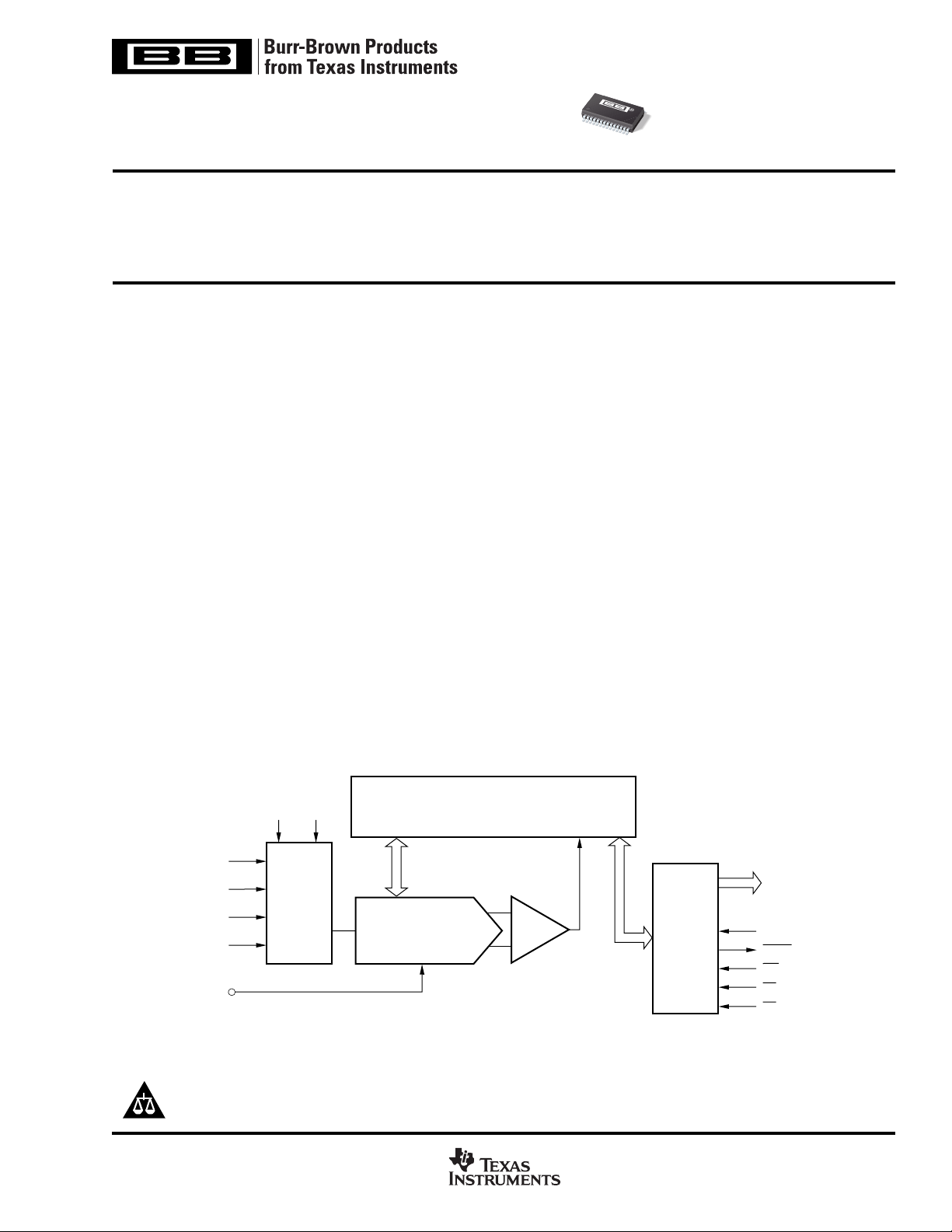
DESCRIPTION
The ADS7842 is a complete, 4-channel, 12-bit Analog-toDigital Converter (ADC). It contains a 12-bit, capacitorbased, Successive Approximation Register (SAR) ADC with
a sample-and-hold amplifier, interface for microprocessor
use, and parallel, 3-state output drivers. The ADS7842 is
specified at a 200kHz sampling rate while dissipating only
2mW of power. The reference voltage can be varied from
100mV to V
24µV to 1.22mV. The ADS7842 is tested down to 2.7V
operation.
Low power, high speed, and an onboard multiplexer make
the ADS7842 ideal for battery-operated systems such as
portable, multi-channel dataloggers and measurement equipment. The ADS7842 is available in an SSOP-28 package
and is tested over the –40°C to +85°C temperature range.
with a corresponding LSB resolution from
CC
A1
A0
AIN0
AIN1
AIN2
AIN3
V
REF
Please be aware that an important notice concerning availability, standard warranty, and use in critical applications of
Texas Instruments semiconductor products and disclaimers thereto appears at the end of this data sheet.
PRODUCTION DATA information is current as of publication date.
Products conform to specifications per the terms of Texas Instruments
standard warranty. Production processing does not necessarily include
testing of all parameters.
4-Channel
MUX
CDAC
SAR
ADS7842
Comparator
www.ti.com
3-State
Parallel
Output
Latches
and
3-State
Drivers
Copyright © 2000, Texas Instruments Incorporated
Data Bus
CLK
BUSY
WR
CS
RD
PACKAGE/ORDERING INFORMATION
MINIMUM
RELATIVE SPECIFIED
PRODUCT (LSB) (dB) PACKAGE-LEAD DESIGNATOR
ACCURACY SINAD PACKAGE TEMPERATURE PACKAGE ORDERING TRANSPORT
ADS7842E ±2 68 SSOP-28 DB –40°C to +85°C ADS7842E ADS7842E Rails, 48
"""""""ADS7842E/1K Tape and Reel, 1000
ADS7842EB ±1 70 SSOP-28 DB –40°C to +85°C ADS7842EB ADS7842EB Rails, 48
"""""""ADS7842EB/1K Tape and Reel, 1000
NOTE: (1) For the most current specifications and package information, refer to our web site at www.ti.com.
(1)
RANGE MARKING NUMBER MEDIA, QUANTITY
ABSOLUTE MAXIMUM RATINGS
+V
to GND ........................................................................–0.3V to +6V
CC
Analog Inputs to GND ............................................ –0.3V to +V
Digital Inputs to GND ........................................................... –0.3V to +6V
Power Dissipation .......................................................................... 250mW
Maximum Junction Temperature................................................... +150°C
Operating Temperature Range ........................................ –40°C to +85°C
Storage Temperature Range ......................................... –65°C to +150°C
Lead Temperature (soldering, 10s)............................................... +300°C
NOTE: (1) Stresses above those listed under “Absolute Maximum Ratings”
may cause permanent damage to the device. Exposure to absolute maximum
conditions for extended periods may affect device reliability.
(1)
+ 0.3V
CC
ELECTROSTATIC
DISCHARGE SENSITIVITY
This integrated circuit can be damaged by ESD. Texas Instruments recommends that all integrated circuits be handled with
appropriate precautions. Failure to observe proper handling
and installation procedures can cause damage.
ESD damage can range from subtle performance degradation to complete device failure. Precision integrated circuits
may be more susceptible to damage because very small
parametric changes could cause the device not to meet its
published specifications.
PIN CONFIGURATION
Top View SSOP
AIN0
AIN1
AIN2
AIN3
V
REF
AGND
DB11
DB10
DB9
DB8
DB7
DB6
DB5
DGND
1
2
3
4
5
6
7
ADS7842E
8
8
10
11
12
13
14
V
28
ANA
27
V
DIG
26
A1
25
A0
24
CLK
23
BUSY
22
WR
21
CS
20
RD
19
DB0
18
DB1
17
DB2
16
DB3
15
DB4
PIN DESCRIPTIONS
PIN NAME DESCRIPTION
1 AIN0 Analog Input Channel 0
2 AIN1 Analog Input Channel 1
3 AIN2 Analog Input Channel 2
4 AIN3 Analog Input Channel 3
5V
6 AGND Analog Ground
7 DB11 Data Bit 11 (MSB)
8 DB10 Data Bit 10
9 DB9 Data Bit 9
10 DB8 Data Bit 8
11 DB7 Data Bit 7
12 DB6 Data Bit 6
13 DB5 Data Bit 5
14 DGND Digital Ground
15 DB4 Data Bit 4
16 DB3 Data Bit 3
17 DB2 Data Bit 2
18 DB1 Data Bit 1
19 DB0 Data Bit 0 (LSB)
20 RD Read Input. Active LOW. Reads the data outputs in
21 CS Chip Select Input. Active LOW. The combination of
22 WR Write Input. Active LOW. Starts a new conversion
23 BUSY BUSY goes LOW and stays LOW during a
24 CLK External Clock Input. The clock speed determines the
25, 26 A0, A1 Address Inputs. Selects one of four analog input
27 V
28 V
Voltage Reference Input. See Electrical Characteris-
REF
tics Tables for ranges.
combination with CS.
CS taken LOW and WR taken LOW initiates a new
conversion and places the outputs in the tri-state
mode.
and selects an analog channel via address inputs A0
and A1, in combination with CS.
conversion. BUSY rises when a conversion is
complete and enables the parallel outputs.
conversion rate by the equation f
channels in combination with CS and WR. The
address inputs are latched on the rising edge of
either RD or WR.
A1 A0 Channel Selected
0 0 AIN0
0 1 AIN1
1 0 AIN2
1 1 AIN3
Digital Supply Input. Nominally +5V.
DIG
Analog Supply Input. Nominally +5V.
ANA
CLK
= 16 • f
SAMPLE
.
2
www.ti.com
ADS7842
SBAS103B
ELECTRICAL CHARACTERISTICS: +5V
At TA = –40°C to +85°C, +VCC = +5V, V
PARAMETER CONDITIONS MIN TYP MAX MIN TYP MAX UNITS
RESOLUTION 12 ✻ Bits
ANALOG INPUT
Full-Scale Input Span 0 V
Capacitance 25 ✻ pF
Leakage Current ±1 ✻ µA
SYSTEM PERFORMANCE
No Missing Codes 12 ✻ Bits
Integral Linearity Error ±2 ±1 LSB
Differential Linearity Error ±0.8 ±0.5 ±1LSB
Offset Error ±3 ✻ LSB
Offset Error Match 0.15 1.0 ✻✻ LSB
Gain Error ±4 ±3LSB
Gain Error Match 0.1 1.0 ✻✻ LSB
Noise 30 ✻ µVrms
Power-Supply Rejection 70 ✻ dB
SAMPLING DYNAMICS
Conversion Time 12 ✻ Clk Cycles
Acquisition Time 3 ✻ Clk Cycles
Throughput Rate 200 ✻ kHz
Multiplexer Settling Time 500 ✻ ns
Aperture Delay 30 ✻ ns
Aperture Jitter 100 ✻ ps
DYNAMIC CHARACTERISTICS
Total Harmonic Distortion
(2)
Signal-to-(Noise + Distortion) V
Spurious-Free Dynamic Range V
Channel-to-Channel Isolation V
REFERENCE INPUT
Range 0.1 +V
Resistance DCLK Static 5 ✻ GΩ
Input Current 40 100 ✻✻ µA
DIGITAL INPUT/OUTPUT
Logic Family CMOS ✻
Logic Levels
V
IH
V
IL
V
OH
V
OL
Data Format Straight Binary ✻
External Clock 0.2 3.2 ✻✻MHz
POWER-SUPPLY REQUIREMENTS
+V
CC
Quiescent Current 550 900 ✻✻ µA
Power Dissipation 4.5 ✻ mW
TEMPERATURE RANGE
Specified Performance –40 +85 ✻✻°C
REF
= +5V, f
= 200kHz, and f
SAMPLE
CLK
= 16 • f
= 3.2MHz, unless otherwise noted.
SAMPLE
ADS7842E ADS7842EB
REF
✻✻V
VIN = 5Vp-p at 10kHz –78 –72 –80 –76 dB
= 5Vp-p at 10kHz 68 71 70 72 dB
IN
= 5Vp-p at 10kHz 72 79 76 81 dB
IN
= 5Vp-p at 50kHz 120 ✻ dB
IN
CC
f
= 12.5kHz 2.5 ✻ µA
SAMPLE
DCLK Static 0.001 3 ✻✻ µA
✻✻V
| IIH | ≤ +5µA 3.0 5.5 ✻✻V
| IIL | ≤ +5µA –0.3 +0.8 ✻✻V
IOH = –250µA 3.5 ✻ V
IOL = 250µA 0.4 ✻ V
Specified Performance 4.75 5.25 ✻✻V
f
= 12.5kHz 300 ✻ µA
SAMPLE
Power-Down Mode
(3)
, CS = +V
CC
3 ✻ µA
(1)
✻ Same specifications as ADS7842E.
NOTES: (1) LSB means Least Significant Bit. With V
at end of conversion when WR, CS, and BUSY conditions have all been met. Refer to Table III of this data sheet.
equal to +5.0V, one LSB is 1.22mV. (2) First five harmonics of the test frequency. (3) Power-down mode
REF
ADS7842
SBAS103B
www.ti.com
3
ELECTRICAL CHARACTERISTICS: +2.7V
At TA = –40°C to +85°C, +VCC = +2.7V, V
PARAMETER CONDITIONS MIN TYP MAX MIN TYP MAX UNITS
RESOLUTION 12 ✻ Bits
ANALOG INPUT
Full-Scale Input Span 0 V
Capacitance 25 ✻ pF
Leakage Current ±1 ✻ µA
SYSTEM PERFORMANCE
No Missing Codes 12 ✻ Bits
Integral Linearity Error ±2 ±1 LSB
Differential Linearity Error ±0.8 ±0.5 ±1LSB
Offset Error ±5 ✻ LSB
Offset Error Match 0.15 1.0 ✻✻ LSB
Gain Error ±4 ±3LSB
Gain Error Match 0.1 1.0 ✻✻ LSB
Noise 30 ✻ µVrms
Power-Supply Rejection 70 ✻ dB
SAMPLING DYNAMICS
Conversion Time 12 ✻ Clk Cycles
Acquisition Time 3 ✻ Clk Cycles
Throughput Rate 125 ✻ kHz
Multiplexer Settling Time 500 ✻ ns
Aperture Delay 30 ✻ ns
Aperture Jitter 100 ✻ ps
DYNAMIC CHARACTERISTICS
Total Harmonic Distortion
(2)
Signal-to-(Noise + Distortion) V
Spurious-Free Dynamic Range V
Channel-to-Channel Isolation V
REFERENCE INPUT
Range 0.1 +V
Resistance DCLK Static 5 ✻ GΩ
Input Current 13 40 ✻✻ µA
DIGITAL INPUT/OUTPUT
Logic Family CMOS ✻
Logic Levels
V
IH
V
IL
V
OH
V
OL
Data Format Straight Binary ✻
External Clock 0.2 2 ✻✻MHz
POWER-SUPPLY REQUIREMENTS
+V
CC
Quiescent Current 280 650 ✻✻ µA
Power Dissipation 1.8 ✻ mW
TEMPERATURE RANGE
Specified Performance –40 +85 ✻✻°C
= +2.5V, f
REF
= 125kHz, and f
SAMPLE
CLK
= 16 • f
= 2MHz, unless otherwise noted.
SAMPLE
ADS7842E ADS7842EB
REF
✻✻V
VIN = 2.5Vp-p at 10kHz –77 –70 –79 –74 dB
= 2.5Vp-p at 10kHz 68 71 70 72 dB
IN
= 2.5Vp-p at 10kHz 72 78 76 80 dB
IN
= 2.5Vp-p at 50kHz 100 ✻ dB
IN
CC
f
= 12.5kHz 2.5 ✻ µA
SAMPLE
DCLK Static 0.001 3 ✻✻ µA
| I
| ≤ +5µA+V
IH
| I
| ≤ +5µA –0.3 +0.8 ✻✻V
IL
IOH = –250µA+V
IOL = 250µA 0.4 ✻ V
• 0.7 5.5 ✻✻V
CC
• 0.8 ✻ V
CC
✻✻V
Specified Performance 2.7 3.6 ✻✻V
f
= 12.5kHz 220 ✻ µA
SAMPLE
Power-Down Mode
(3)
, CS = +V
CC
3 ✻ µA
(1)
✻ Same specifications as ADS7842E.
NOTES: (1) LSB means Least Significant Bit. With V
at end of conversion when WR, CS, and BUSY conditions have all been met. Refer to Table III of this data sheet.
4
equal to +2.5V, one LSB is 610mV. (2) First five harmonics of the test frequency. (3) Power-down mode
REF
www.ti.com
ADS7842
SBAS103B
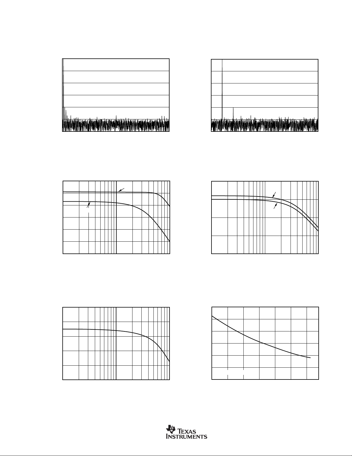
TYPICAL CHARACTERISTICS: +5V
0
–20
–40
–60
–80
–100
–120
FREQUENCY SPECTRUM
(4096 Point FFT; f
IN
= 10.3kHz, –0.2dB)
0 10025 7550
Frequency (kHz)
Amplitude (dB)
At TA = +25°C, +VCC = +5V, V
(4096 Point FFT; f
0
–20
–40
–60
–80
Amplitude (dB)
–100
–120
0 10025 7550
= +5V, f
REF
FREQUENCY SPECTRUM
IN
Frequency (kHz)
= 200kHz, and f
SAMPLE
= 1,123Hz, –0.2dB)
CLK
= 16 • f
SAMPLE
= 3.2MHz, unless otherwise noted.
SIGNAL-TO-NOISE RATIO AND SIGNAL-TO-
74
73
72
71
70
SNR and SINAD (dB)
69
68
12.0
11.8
11.6
11.4
Effective Number of Bits
11.2
11.0
(NOISE + DISTORTION) vs INPUT FREQUENCY
SNR
SINAD
101 100
Input Frequency (kHz)
EFFECTIVE NUMBER OF BITS
vs INPUT FREQUENCY
101 100
Input Frequency (kHz)
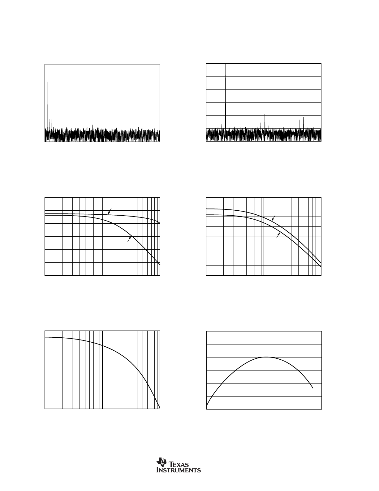
SFDR (dB)
–0.2
Delta from +25°C (dB)
–0.4
–0.6
SPURIOUS-FREE DYNAMIC RANGE AND TOTAL
HARMONIC DISTORTION vs INPUT FREQUENCY
85
SFDR
80
75
70
65
Input Frequency (kHz)
CHANGE IN SIGNAL-TO-(NOISE + DISTORTION)
0.6
0.4
0.2
0.0
fIN = 10kHz, –0.2dB
–20–40 100
vs TEMPERATURE
0 20 40 60 80
Temperature (°C)
THD
101100
–85
–80
–75
THD (dB)
–70
–65
ADS7842
SBAS103B
www.ti.com
5
TYPICAL CHARACTERISTICS: +2.7V
At TA = +25°C, +VCC = +2.7V, V
= +2.5V, f
REF
= 125kHz, and f
SAMPLE
CLK
= 16 • f
SAMPLE
= 2MHz, unless otherwise noted.
(4096 Point FFT; f
0
–20
–40
–60
–80
Amplitude (dB)
–100
–120
0 62.515.6 46.931.3
SIGNAL-TO-NOISE RATIO AND SIGNAL-TO-
(NOISE + DISTORTION) vs INPUT FREQUENCY
78
74
70
66
62
SNR and SINAD (dB)
58
54
FREQUENCY SPECTRUM
Input Frequency (kHz)
= 1,129Hz, –0.2dB)
IN
Frequency (kHz)
SNR
SINAD
101 100
(4096 Point FFT; f
0
–20
–40
–60
–80
Amplitude (dB)
–100
–120
0 62.515.6 46.931.3
SPURIOUS-FREE DYNAMIC RANGE AND TOTAL
HARMONIC DISTORTION vs INPUT FREQUENCY
90
85
80
75
70
65
SFDR (dB)
60
55
50
FREQUENCY SPECTRUM
Input Frequency (kHz)
= 10.6kHz, –0.2dB)
IN
Frequency (kHz)
SFDR
THD
101 100
–90
–85
–80
–75
–70
–65
–60
–55
–50
THD (dB)
12.0
11.5
11.0
10.5
10.0
Effective Number of Bits
9.5
9.0
6
EFFECTIVE NUMBER OF BITS
vs INPUT FREQUENCY
101 100
Input Frequency (kHz)
www.ti.com
0.4
0.2
0.0
–0.2
–0.4
Delta from +25°C (dB)
–0.6
–0.8
CHANGE IN SIGNAL-TO-(NOISE + DISTORTION)
fIN = 10kHz, –0.2dB
–20–40 100
vs TEMPERATURE
0 20 40 60 80
Temperature (°C)
ADS7842
SBAS103B
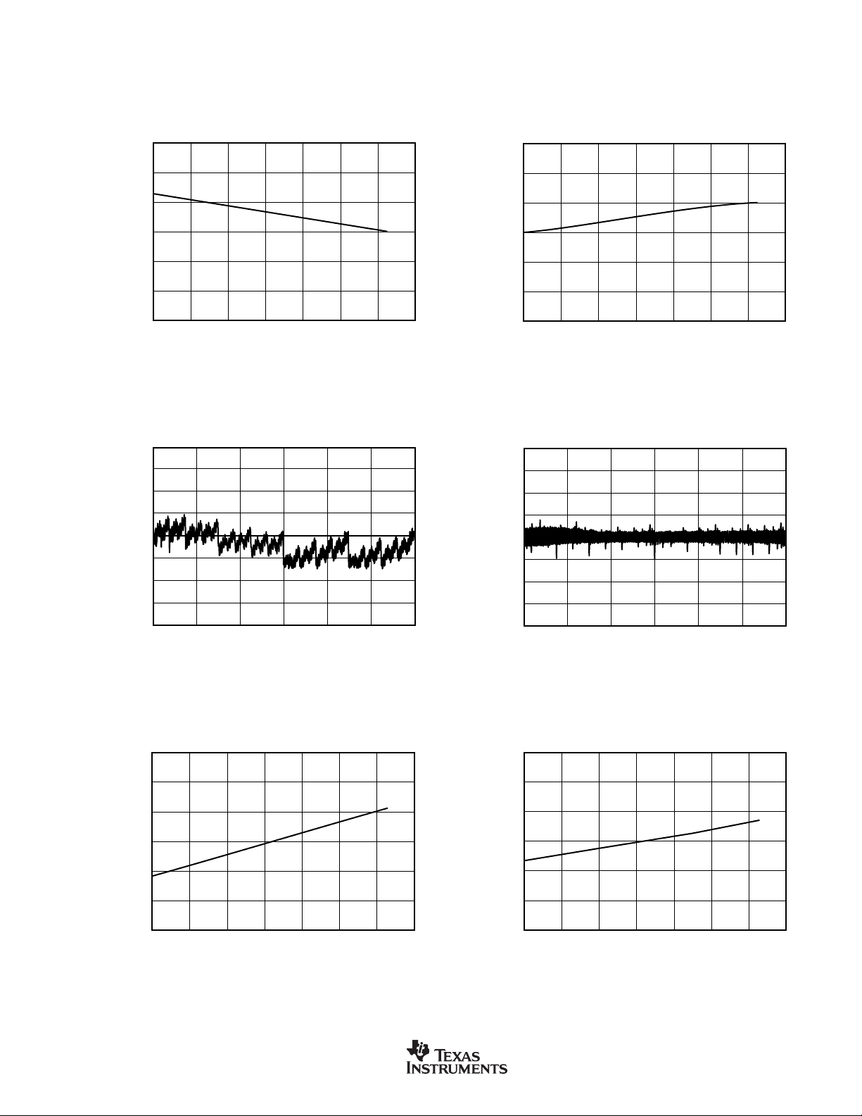
TYPICAL CHARACTERISTICS: +2.7V (Cont.)
Output Code
1.00
0.75
0.50
0.25
0.00
–0.25
–0.50
–0.75
–1.00
DIFFERENTIAL LINEARITY ERROR vs CODE
800
H
FFF
H
000
H
DLE (LSB)
At TA = +25°C, +VCC = +2.7V, V
SUPPLY CURRENT vs TEMPERATURE
400
= +2.5V, f
REF
= 125kHz, and f
SAMPLE
= 16 • f
CLK
= 2MHz, unless otherwise noted.
SAMPLE
140
POWER-DOWN SUPPLY CURRENT
vs TEMPERATURE
350
300
250
200
Supply Current (µA)
150
100
1.00
0.75
0.50
0.25
0.00
ILE (LSB)
–0.25
–0.50
–0.75
–1.00
000
20–40 100–20 0 40
Temperature (°C)
INTEGRAL LINEARITY ERROR vs CODE
800
H
H
Output Code
60 80
FFF
120
100
80
60
Supply Current (nA)
40
20
20–40 100–20 0 40
60 80
Temperature (°C)
H
0.15
CHANGE IN GAIN vs TEMPERATURE
0.10
0.05
0.00
–0.05
Delta from +25°C (LSB)
–0.10
–0.15
ADS7842
SBAS103B
20–40 100–20 0 40
Temperature (°C)
60 80
www.ti.com
0.6
0.4
0.2
0.0
–0.2
Delta from +25°C (LSB)
–0.4
–0.6
CHANGE IN OFFSET vs TEMPERATURE
20–40 100–20 0 40
60 80
Temperature (°C)
7
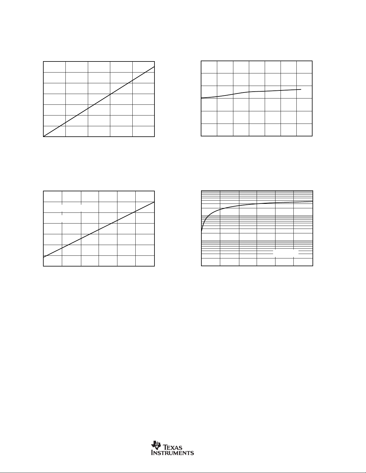
TYPICAL CHARACTERISTICS: +2.7V (Cont.)
At TA = +25°C, +VCC = +2.7V, V
= +2.5V, f
REF
= 125kHz, and f
SAMPLE
= 16 • f
CLK
= 2MHz, unless otherwise noted.
SAMPLE
Reference Current (µA)
14
12
10
320
300
280
260
REFERENCE CURRENT vs SAMPLE RATE
REFERENCE CURRENT vs TEMPERATURE
18
16
14
8
12
6
4
2
0
75012525 50 100
Sample Rate (kHz)
SUPPLY CURRENT vs +V
CC
10
Reference Current (µA)
8
6
20–40 100–20 0 40
60 80
Temperature (°C)
MAXIMUM SAMPLE RATE vs +V
CC
1M
f
= 12.5kHz
SAMPLE
= +V
CC
V
REF
100k
240
10k
220
Supply Current (µA)
200
180
3.5252.5 4
(V)
+V
CC
4.53
Sample Rate (Hz)
1k
3.5252.5 4
(V)
+V
CC
V
REF
= +VCC
4.53
8
www.ti.com
ADS7842
SBAS103B

THEORY OF OPERATION
The ADS7842 is a classic SAR ADC. The architecture is
based on capacitive redistribution which inherently includes
a sample-and-hold function. The converter is fabricated on a
0.6µm CMOS process.
The basic operation of the ADS7842 is shown in Figure 1.
The device requires an external reference and an external
clock. It operates from a single supply of 2.7V to 5.25V. The
external reference can be any voltage between 100mV and
+V
. The value of the reference voltage directly sets the
CC
input range of the converter. The average reference input
current depends on the conversion rate of the ADS7842.
some operating modes. While the converter is in the hold
mode, or after the sampling capacitor has been fully charged,
the input impedance of the analog input is greater than 1GΩ.
EXTERNAL CLOCK
The ADS7842 requires an external clock to run the conversion process. This clock can vary between 200kHz (12.5kHz
throughput) and 3.2MHz (200kHz throughput). The duty
cycle of the clock is unimportant as long as the minimum
HIGH and LOW times are at least 150ns and the clock period
is at least 300ns. The minimum clock frequency is set by the
leakage on the capacitors internal to the ADS7842.
ANALOG INPUTS
The ADS7842 features four, single-ended inputs. The input
current into each analog input depends on input voltage and
sampling rate. Essentially, the current into the device must
charge the internal hold capacitor during the sample period.
After this capacitance has fully charged, there is no further
input current. The source of the analog input voltage must be
able to charge the input capacitance to a 12-bit settling level
within the same period, which can be as little as 350ns in
ADS7842
0V to V
REF
+5V
+
2.2µF
1
AIN0
2
AIN1
3
AIN2
4
AIN3
5
V
REF
6
AGND
7
DB11
8
DB10
9
DB9
10
DB8
11
DB7
12
DB6
13
DB5
14
DGND
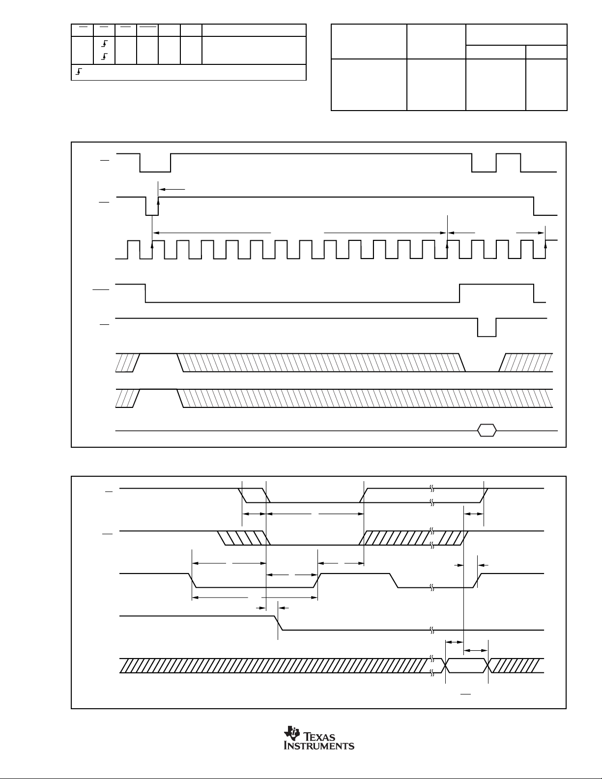
BASIC OPERATION
Figure 1 shows the simple circuit required to operate the
ADS7842 with Channel 0 selected. A conversion can be
initiated by bringing the
of 25ns.
BUSY
conversion process and rises only after the conversion is
complete. The 12 bits of output data will be valid on pins
7-13 and 15-19 following the rising edge of
28
V
ANA
V
DIG
A1
A0
CLK
BUSY
WR
CS
RD
DB0
DB1
DB2
DB3
DB4
27
26
25
24
23
22
21
20
19
18
17
16
15
0.1µF+10µF
WR
pin (pin 22) LOW for a minimum
(pin 23) will output a LOW during the
BUSY
+
+5V Analog Supply
3.2MHz Clock
BUSY Output
Write Input
Read Input
.
FIGURE 1. Basic Operation of the ADS7842.
ADS7842
SBAS103B
www.ti.com
9
STARTING A CONVERSION
A conversion is initiated on the falling edge of the WR input,
with valid signals on A0, A1, and
CS
. The ADS7842 will
enter the conversion mode on the first rising edge of the
external clock following the
WR
pin going LOW. The ADS7842
will start the conversion on the 1st clock cycle. The MSB will
be approximated by the Capacitive Digital-to-Analog Converter (CDAC) on the 1st clock cycle, the 2nd-MSB on the
2nd cycle, and so on until the LSB has been decided on the
12th clock cycle. The
the falling edge of the
BUSY
output will go LOW 20ns after
WR
pin. The
BUSY
output will return
HIGH just after the ADS7842 has finished a conversion and
the data will be valid on pins 7-13, 15-19. The rising edge of
BUSY
can be used to latch the data. It is recommended that
the data be read immediately after each conversion. The
switching noise of the asynchronous data transfer can cause
digital feedthrough degrading the converter’s performance.
See Figure 2.
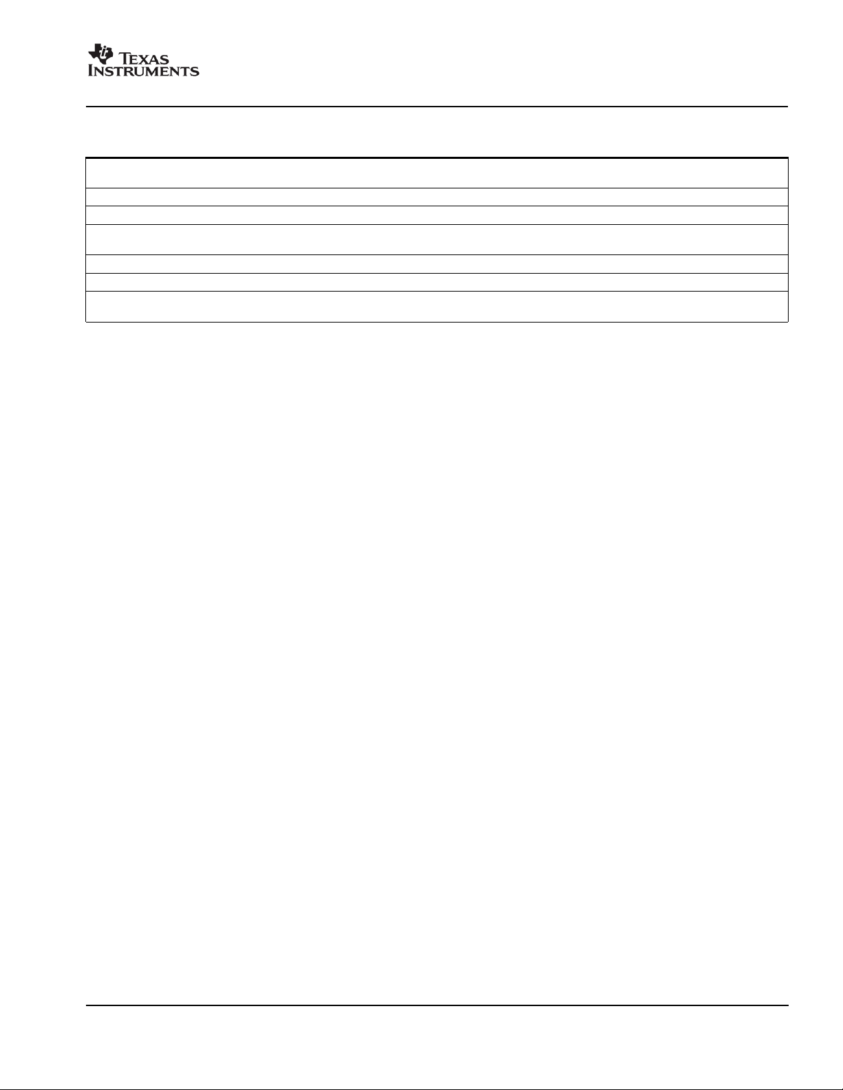
READING DATA
Data from the ADS7842 will appear at pins 7-13 and
15-19. The MSB will output on pin 7 while the LSB will
output on pin 19. The outputs are coded in Straight Binary
(with 0V = 000
a conversion, the
HIGH, the
the 12-bit output bus.
least 25ns seconds following
25ns seconds after the falling edge of both
and V
H
BUSY
CS
and RD pins may be brought LOW to enable
= FFFH, see Table IV). Following
REF
pin will go HIGH. After
CS
and RD must be held LOW for at
BUSY
HIGH. Data will be valid
BUSY
CS
and RD. The
goes
output data will remain valid for 25ns seconds following the
rising edge of both
CS
and RD. See Figure 4 for the read
cycle timing diagram.
POWER-DOWN MODE
The ADS7842 incorporates a unique method of placing the
ADC in the power-down mode. Rather than adding an extra
pin to the package, the A0 address pin is used in conjunction
with the
also to ‘wake-up’ the ADC following power-down. In this
shutdown mode, all analog and digital circuitry is turned off.
The simplest way to place the ADS7842 in power-down
mode is immediately following a conversion. After a conversion has been completed and the
HIGH,
25ns. While keeping
ADS7842 enters the power-down mode, provided the A0 pin
is HIGH (see Figure 5 and Table III). In order to ‘wake-up’ the
device following power-down, A0 must be LOW when
switches from LOW to HIGH a second time (see Figure 6).
The typical supply current of the ADS7842 with a 5V supply
and 200kHz sampling rate is 550µA. In the power-down
mode the current is typically reduced to 3µA.
RD
pin to place the device in power-down mode and
BUSY
output has returned
CS
and RD must be brought LOW for a minimum of
CS
LOW, RD is brought HIGH and the
RD
SYMBOL DESCRIPTION MIN TYP MAX UNITS
t
CONV
t
ACQ
t
CKP
t
CKL
t
CKH
t
1
t
2
t
3
t
4
t
5
t
6
t
7
t
8
t
9
t
10
t
11
t
12
t
13
t
14
t
15
t
16
t
17
TABLE I. Timing Specifications (+V
SYMBOL DESCRIPTION MIN TYP MAX UNITS
t
CONV
t
ACQ
t
CKP
t
CKL
t
CKH
t
1
t
2
t
3
t
4
t
5
t
6
t
7
t
8
t
9
t
10
t
11
t
12
t
13
t
14
t
15
t
16
t
17
Conversion Time 6.5 µs
Acquisition Time 1.5 µs
Clock Period 500 ns
Clock LOW 150 ns
Clock HIGH 150 ns
CS to WR/RD Setup Time 0 ns
Address to CS Hold Time 0 ns
CS LOW 25 ns
CLK to WR Setup Time 25 ns
CS to BUSY LOW 20 ns
CLK to WR LOW 5 ns
CLK to WR HIGH 25 ns
WR to CLK HIGH 25 ns
Address Hold Time 5 ns
Address Setup Time 5 ns
BUSY to RD Delay 0 ns
CLK LOW to BUSY HIGH 10 ns
BUS Access 25 ns
BUS Relinquish 25 ns
Address to RD HIGH 2 ns
Address Hold Time 2 ns
RD HIGH to CLK LOW 50 ns
= +2.7V to 3.6V,
T
= –40°C to +85°C, C
A
Conversion Time 3.5 µs
Acquisition Time 1.5 µs
Clock Period 300 ns
Clock LOW 150 ns
Clock HIGH 150 ns
CS to WR/RD Setup Time 0 ns
Address to CS Hold Time 0 ns
CS LOW 25 ns
CLK to WR Setup Time 25 ns
CS to BUSY LOW 20 ns
CLK to WR LOW 5 ns
CLK to WR HIGH 25 ns
WR to CLK HIGH 25 ns
Address Hold Time 5 ns
Address Setup Time 5 ns
BUSY to RD Delay 0 ns
CLK LOW to BUSY HIGH 10 ns
BUS Access 25 ns
BUS Relinquish 25 ns
Address to RD HIGH 2 ns
Address Hold Time 2 ns
RD HIGH to CLK LOW 50 ns
CC
LOAD
= 50pF).
TABLE II. Timing Specifications (+VCC = +4.75V to +5.25V,
T
= –40°C to +85°C, C
A
LOAD
= 50pF).
10
www.ti.com
ADS7842
SBAS103B
CS RD WR BUSY A0 A1 COMMENTS
0X11X
0X10X
Power-Down Mode
Wake-Up Mode
means rising edge triggered. X = Don't care.
TABLE III. Truth Table for Power-Down and Wake-Up Modes.
DIGITAL OUTPUT
STRAIGHT BINARY
DESCRIPTION ANALOG INPUT BINARY CODE HEX CODE
Least Significant Bit (LSB)
1.2207mV
Full-Scale 4.99878V 1111 1111 1111 FFF
Midscale 2.5V 1000 0000 0000 800
Midscale –1LSB 2.49878V 0111 1111 1111 7FF
Zero Full-Scale 0V 0000 0000 0000 000
CS
WR
CLK
BUSY
RD
A0
A1
Latching in Address for Next Channel
123
45
TABLE IV. Ideal Input Voltages and Output Codes (V
Conversion
678
REF
Sample
910111213141516
= 5V).
DB0-DB11
FIGURE 2. Normal Operation, 16 Clocks per Conversion.
CS
t
1
WR
t
CLK
BUSY
A0, A1
6
t
CKL
NOTE: (1) Addresses for next conversion (N + 1) latched in with rising edge of current WR (N).
t
4
t
DATA VALID
t
t
10
N + 1
2
t
8
t
9
(1)
t
3
t
7
5
FIGURE 3. Initiating a Conversion.
ADS7842
SBAS103B
www.ti.com
11

CS
t
1
t
3
RD
CLK
t
12
t
11
BUSY
n – 1
A0
t
13
DB0-DB11
n-1 DATA VALID
NOTE: Internal register of current conversion updated 1/2 clock cycle prior to BUSY going HIGH.
FIGURE 4. Read Timing Following a Conversion.
CS
t
1
RD
t
3
Conversion n
To prevent PWD
A0 must be 0
t
14
t
2
CLK
t
12
t
11
BUSY
A0
NOTE: Rising edge of RD while A0 = 1 initiates power down immediately.
FIGURE 5. Entering Power-Down Using RD and A0.
CS
t
1
RD
A0
NOTE: Rising edge of 2nd RD while A0 = 0 places the ADS7842 in sample mode.
t
3
t
15
t
15t16
t
16
t
2
FIGURE 6. Initiating Wake-Up Using RD and A0.
12
www.ti.com
ADS7842
SBAS103B

REFERENCE INPUT
The external reference sets the analog input range. The
ADS7842 will operate with a reference in the range of 100mV
to +V
There are several critical items concerning the reference
input and its wide voltage range. As the reference voltage is
reduced, the analog voltage weight of each digital output
code is also reduced. This is often referred to as the LSB size
and is equal to the reference voltage divided by 4096. Any
offset or gain error inherent in the ADC will appear to
increase, in terms of LSB size, as the reference voltage is
reduced. For example, if the offset of a given converter is
2LSBs with a 2.5V reference, then it will typically be 10LSBs
with a 0.5V reference. In each case, the actual offset of the
device is the same, 1.22mV.
Likewise, the noise or uncertainty of the digitized output will
increase with lower LSB size. With a reference voltage of
100mV, the LSB size is 24µV. This level is below the internal
noise of the device. As a result, the digital output code will not
be stable and vary around a mean value by a number of
LSBs. The distribution of output codes will be gaussian and
the noise can be reduced by simply averaging consecutive
conversion results or applying a digital filter.
With a lower reference voltage, care should be taken to
provide a clean layout including adequate bypassing, a clean
(low-noise, low-ripple) power supply, a low-noise reference,
and a low-noise input signal. Because the LSB size is lower,
the converter will also be more sensitive to nearby digital
signals and electromagnetic interference.
The voltage into the V
drives the CDAC portion of the ADS7842. Typically, the input
current is 13µA with a 2.5V reference. This value will vary by
microamps depending on the result of the conversion. The
reference current diminishes directly with both conversion
rate and reference voltage. As the current from the reference
is drawn on each bit decision, clocking the converter more
quickly during a given conversion period will not reduce
overall current drain from the reference.
CC
.
input is not buffered and directly
REF
Data Format
The ADS7842 output data is in Straight Offset Binary format,
see Table IV. This table shows the ideal output code for the
given input voltage and does not include the effects of offset,
gain, or noise.
LAYOUT
For optimum performance, care should be taken with the
physical layout of the ADS7842 circuitry. This is particularly
true if the reference voltage is low and/or the conversion rate
is high.
The basic SAR architecture is sensitive to glitches or sudden
changes on the power supply, reference, ground connections, and digital inputs that occur just prior to latching the
output of the analog comparator. Thus, during any single
conversion for an n-bit SAR converter, there are n “windows”
in which large external transient voltages can easily affect the
conversion result. Such glitches might originate from switching power supplies, nearby digital logic, and high-power
devices. The degree of error in the digital output depends on
the reference voltage, layout, and the exact timing of the
external event. The error can change if the external event
changes in time with respect to the DCLK input.
With this in mind, power to the ADS7842 should be clean and
well bypassed. A 0.1µF ceramic bypass capacitor should be
placed as close to the device as possible. In addition, a 1µF
to 10µF capacitor and a 5Ω or 10Ω series resistor may be
used to low-pass filter a noisy supply.
The reference should be similarly bypassed with a 0.1µF
capacitor. Again, a series resistor and large capacitor can be
used to low-pass filter the reference voltage. If the reference
voltage originates from an op amp, make sure that it can
drive the bypass capacitor without oscillation (the series
resistor can help in this case). The ADS7842 draws very little
current from the reference on average, but it does place
larger demands on the reference circuitry over short periods
of time (on each rising edge of CLK during a conversion).
The ADS7842 architecture offers no inherent rejection of
noise or voltage variation in regards to the reference input.
This is of particular concern when the reference input is tied
to the power supply. Any noise and ripple from the supply will
appear directly in the digital results. While high frequency
noise can be filtered out as discussed in the previous
paragraph, voltage variation due to line frequency (50Hz or
60Hz) can be difficult to remove.
The GND pin should be connected to a clean ground point. In
many cases, this will be the “analog” ground. Avoid connections which are too near the grounding point of a microcontroller
or digital signal processor. If needed, run a ground trace
directly from the converter to the power-supply entry point. The
ideal layout will include an analog ground plane dedicated to
the converter and associated analog circuitry.
ADS7842
SBAS103B
www.ti.com
13

PACKAGE DRAWING
MSSO002D – JANUARY 1995 – REVISED SEPTEMBER 2000
DB (R-PDSO-G**) PLASTIC SMALL-OUTLINE
28 PINS SHOWN
0,65
28
1
0,38
0,22
15
14
A
0,15
5,60
5,00
M
8,20
7,40
Seating Plane
0,15 NOM
Gage Plane
0°–8°
0,25
0,95
0,55
2,00 MAX
PINS **
DIM
A MAX
A MIN
NOTES: A. All linear dimensions are in millimeters.
B. This drawing is subject to change without notice.
C. Body dimensions do not include mold flash or protrusion not to exceed 0,15.
D. Falls within JEDEC MO-150
14
6,50
0,05 MIN
6,50
5,905,90
2016
7,50
6,90
24
8,50
0,10
28
10,50
9,907,90
30
10,50
9,90
38
12,90
12,30
4040065 /D 09/00
14
www.ti.com
ADS7842
SBAS103B
PACKAGE OPTION ADDENDUM
www.ti.com
30-Mar-2005
PACKAGING INFORMATION
Orderable Device Status
(1)
Package
Type
Package
Drawing
Pins Package
Qty
Eco Plan
ADS7842E ACTIVE SSOP DB 28 48 TBD CU NIPDAU Level-3-220C-168 HR
ADS7842E/1K ACTIVE SSOP DB 28 1000 TBD CU NIPDAU Level-3-220C-168 HR
ADS7842E/1KG4 ACTIVE SSOP DB 28 1000 Green (RoHS &
no Sb/Br)
ADS7842EB ACTIVE SSOP DB 28 48 TBD CU NIPDAU Level-3-220C-168 HR
ADS7842EB/1K ACTIVE SSOP DB 28 1000 TBD CU NIPDAU Level-3-220C-168 HR
ADS7842EG4 ACTIVE SSOP DB 28 48 Green (RoHS &
no Sb/Br)
(1)
The marketing status values are defined as follows:
ACTIVE: Product device recommended for new designs.
LIFEBUY: TI has announced that the device will be discontinued, and a lifetime-buy period is in effect.
NRND: Not recommended for new designs. Device is in production to support existing customers, but TI does not recommend using this part in
a new design.
PREVIEW: Device has been announced but is not in production. Samples may or may not be available.
OBSOLETE: TI has discontinued the production of the device.
(2)
Eco Plan - The planned eco-friendly classification: Pb-Free (RoHS) or Green (RoHS & no Sb/Br) - please check
http://www.ti.com/productcontent for the latest availability information and additional product content details.
TBD: The Pb-Free/Green conversion plan has not been defined.
Pb-Free (RoHS): TI's terms "Lead-Free" or "Pb-Free" mean semiconductor products that are compatible with the current RoHS requirements
for all 6 substances, including the requirement that lead not exceed 0.1% by weight in homogeneous materials. Where designed to be soldered
at high temperatures, TI Pb-Free products are suitable for use in specified lead-free processes.
Green (RoHS & no Sb/Br): TI defines "Green" to mean Pb-Free (RoHS compatible), and free of Bromine (Br) and Antimony (Sb) based flame
retardants (Br or Sb do not exceed 0.1% by weight in homogeneous material)
(2)
Lead/Ball Finish MSL Peak Temp
CU NIPDAU Level-2-260C-1 YEAR
CU NIPDAU Level-2-260C-1 YEAR
(3)
(3)
MSL, Peak Temp. -- The Moisture Sensitivity Level rating according to the JEDEC industry standard classifications, and peak solder
temperature.
Important Information and Disclaimer:The information provided on this page represents TI's knowledge and belief as of the date that it is
provided. TI bases its knowledge and belief on information provided by third parties, and makes no representation or warranty as to the
accuracy of such information. Efforts are underway to better integrate information from third parties. TI has taken and continues to take
reasonable steps to provide representative and accurate information but may not have conducted destructive testing or chemical analysis on
incoming materials and chemicals. TI and TI suppliers consider certain information to be proprietary, and thus CAS numbers and other limited
information may not be available for release.
In no event shall TI's liability arising out of such information exceed the total purchase price of the TI part(s) at issue in this document sold by TI
to Customer on an annual basis.
Addendum-Page 1

IMPORTANT NOTICE
Texas Instruments Incorporated and its subsidiaries (TI) reserve the right to make corrections, modifications,
enhancements, improvements, and other changes to its products and services at any time and to discontinue
any product or service without notice. Customers should obtain the latest relevant information before placing
orders and should verify that such information is current and complete. All products are sold subject to TI’s terms
and conditions of sale supplied at the time of order acknowledgment.
TI warrants performance of its hardware products to the specifications applicable at the time of sale in
accordance with TI’s standard warranty. Testing and other quality control techniques are used to the extent TI
deems necessary to support this warranty . Except where mandated by government requirements, testing of all
parameters of each product is not necessarily performed.
TI assumes no liability for applications assistance or customer product design. Customers are responsible for
their products and applications using TI components. To minimize the risks associated with customer products
and applications, customers should provide adequate design and operating safeguards.
TI does not warrant or represent that any license, either express or implied, is granted under any TI patent right,
copyright, mask work right, or other TI intellectual property right relating to any combination, machine, or process
in which TI products or services are used. Information published by TI regarding third-party products or services
does not constitute a license from TI to use such products or services or a warranty or endorsement thereof.
Use of such information may require a license from a third party under the patents or other intellectual property
of the third party, or a license from TI under the patents or other intellectual property of TI.
Reproduction of information in TI data books or data sheets is permissible only if reproduction is without
alteration and is accompanied by all associated warranties, conditions, limitations, and notices. Reproduction
of this information with alteration is an unfair and deceptive business practice. TI is not responsible or liable for
such altered documentation.
Resale of TI products or services with statements different from or beyond the parameters stated by TI for that
product or service voids all express and any implied warranties for the associated TI product or service and
is an unfair and deceptive business practice. TI is not responsible or liable for any such statements.
Following are URLs where you can obtain information on other Texas Instruments products and application
solutions:
Products Applications
Amplifiers amplifier.ti.com Audio www.ti.com/audio
Data Converters dataconverter.ti.com Automotive www.ti.com/automotive
DSP dsp.ti.com Broadband www.ti.com/broadband
Interface interface.ti.com Digital Control www.ti.com/digitalcontrol
Logic logic.ti.com Military www.ti.com/military
Power Mgmt power.ti.com Optical Networking www.ti.com/opticalnetwork
Microcontrollers microcontroller.ti.com Security www.ti.com/security
Telephony www.ti.com/telephony
Video & Imaging www.ti.com/video
Wireless www.ti.com/wireless
Mailing Address: Texas Instruments
Post Office Box 655303 Dallas, Texas 75265
Copyright 2005, Texas Instruments Incorporated
 Loading...