ADS7822
ADS7822
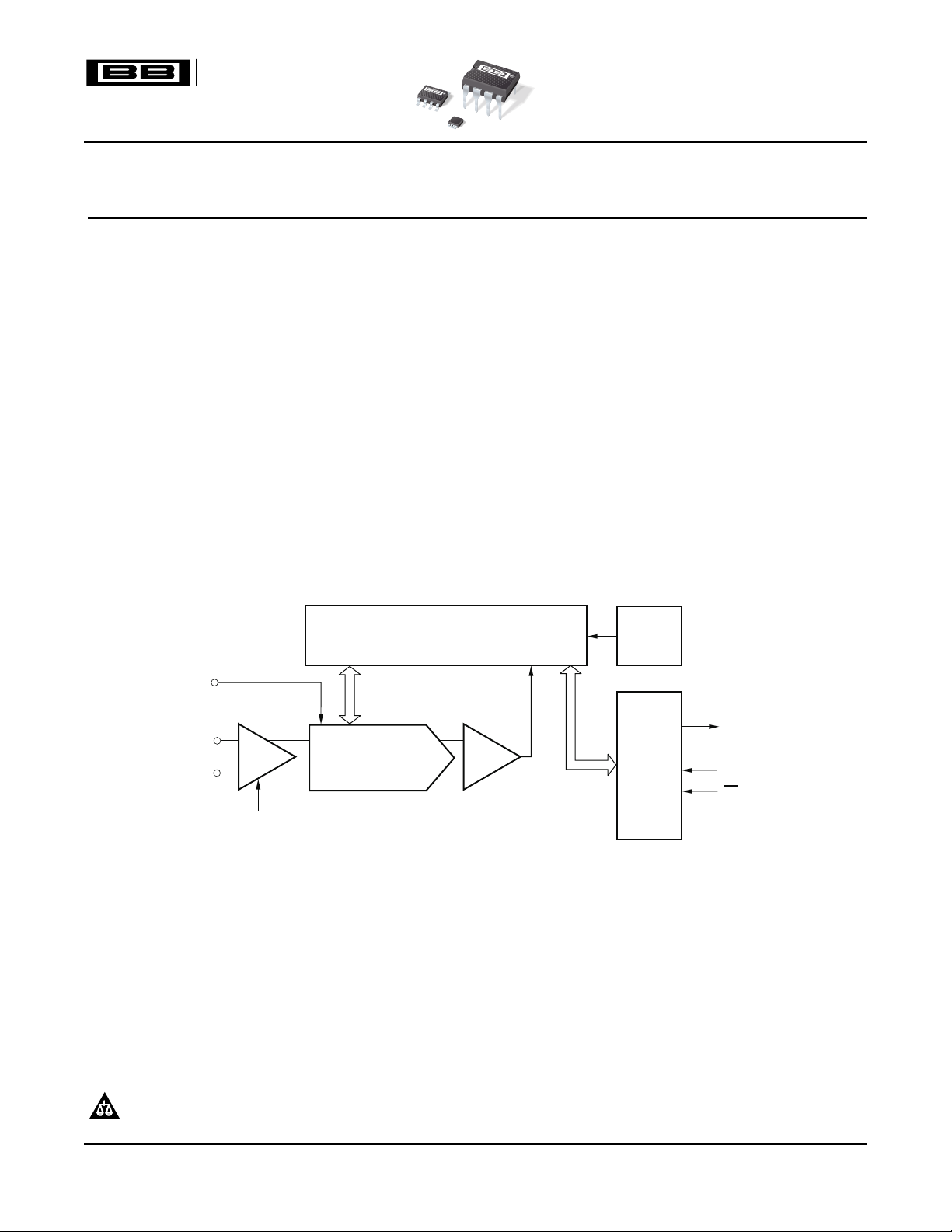
SAR
Control
Serial
Interface
D
OUT
Comparator
S/HAmp
CS/SHDN
DCLOCK
+In
V
REF
-In
CDAC
12-Bit, 200kHz, microPower Sampling
ANALOG-TO-DIGITAL CONVERTER
FEATURES DESCRIPTION
• 200kHz Sampling Rate
• microPower:
1.6mW at 200kHz
0.54mW at 75kHz
0.06mW at 7.5kHz
• Power Down: 3 µ A max
• Mini-DIP-8, SO-8, and MSOP-8 Packages
• Pseudo-Differential Input
• Serial Interface
APPLICATIONS
• Battery-Operated Systems
• Remote Data Acquisition
• Isolated Data Acquisition
• Simultaneous Sampling, Multichannel
Systems
ADS7822
SBAS062B – JANUARY 1996 – REVISED MAY 2006
The ADS7822 is a 12-bit sampling analog-to-digital
(A/D) converter with ensured specifications over a
2.7V to 5.25V supply range. It requires very little
power even when operating at the full 200kHz rate.
At lower conversion rates, the high speed of the
device enables it to spend most of its time in the
power-down mode—the power dissipation is less
than 60 µ W at 7.5kHz.
The ADS7822 also features operation from 2.0V to
5V, a synchronous serial interface, and a
pseudo-differential input. The reference voltage can
be set to any level within the range of 50mV to V
Ultra low power and small size make the ADS7822
ideal for battery-operated systems. It is also a perfect
fit for remote data-acquisition modules, simultaneous
multichannel systems, and isolated data acquisition.
The ADS7822 is available in a plastic mini-DIP-8, an
SO-8, or an MSOP-8 package.
CC
.
Please be aware that an important notice concerning availability, standard warranty, and use in critical applications of Texas
Instruments semiconductor products and disclaimers thereto appears at the end of this data sheet.
All trademarks are the property of their respective owners.
PRODUCTION DATA information is current as of publication date.
Products conform to specifications per the terms of the Texas
Instruments standard warranty. Production processing does not
necessarily include testing of all parameters.
Copyright © 1996–2006, Texas Instruments Incorporated
www.ti.com
ADS7822
SBAS062B – JANUARY 1996 – REVISED MAY 2006
This integrated circuit can be damaged by ESD. Texas Instruments recommends that all integrated circuits be handled with
appropriate precautions. Failure to observe proper handling and installation procedures can cause damage.
ESD damage can range from subtle performance degradation to complete device failure. Precision integrated circuits may be
more susceptible to damage because very small parametric changes could cause the device not to meet its published
specifications.
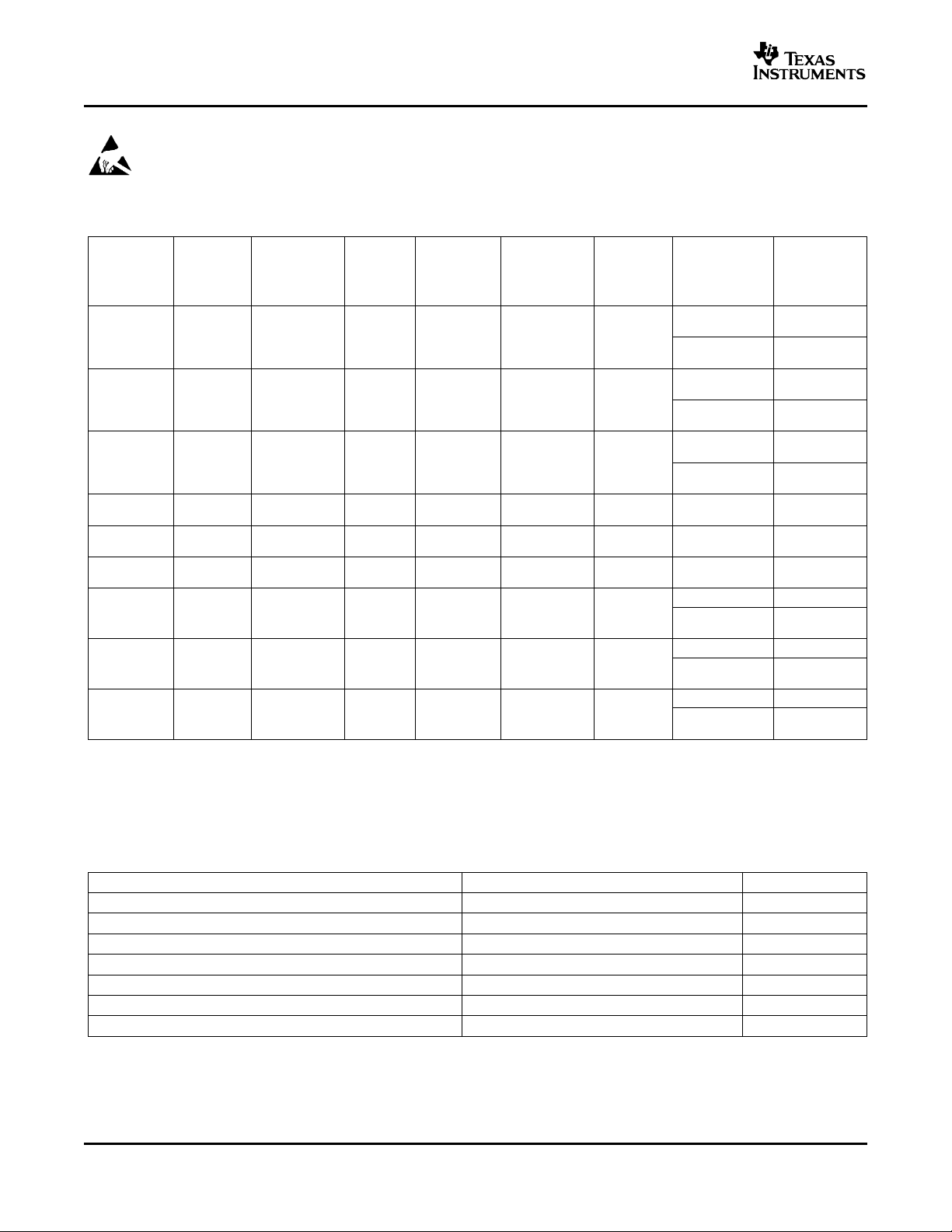
ORDERING INFORMATION
MAXIMUM MAXIMUM
INTEGRAL DIFFERENTIAL
LINEARITY LINEARITY SPECIFIED TRANSPORT
PRODUCT (LSB) (LSB) LEAD DESIGNATOR RANGE MARKING
ADS7822E ± 2 ± 2 MSOP-8 DGK –40 ° C to +85 ° C A22
ADS7822EB ± 1 ± 1 MSOP-8 DGK –40 ° C to +85 ° C A22
ADS7822EC ± 0.75 ± 0.75 MSOP-8 DGK –40 ° C to +85 ° C A22
ADS7822P ± 2 ± 2 P –40 ° C to +85 ° C ADS7822P ADS7822P Rails, 50
ADS7822PB ± 1 ± 1 P –40 ° C to +85 ° C ADS7822PB ADS7822PB Rails, 50
ADS7822PC ± 0.75 ± 0.75 P –40 ° C to +85 ° C ADS7822PC ADS7822PC Rails, 50
ADS7822U ± 2 ± 2 SO-8 D –40 ° C to +85 ° C ADS7822U
ADS7822UB ± 1 ± 1 SO-8 D –40 ° C to +85 ° C ADS7822UB
ADS7822UC ± 0.75 ± 0.75 SO-8 D –40 ° C to +85 ° C ADS7822UC
ERROR ERROR PACKAGE- PACKAGE TEMPERATURE PACKAGE ORDERING MEDIA,
Plastic
DIP-8
Plastic
DIP-8
Plastic
DIP-8
(1)
(2)
NUMBER QUANTITY
ADS7822E/250
ADS7822E/2K5
ADS7822EB/250
ADS7822EB/2K5
ADS7822EC/250
ADS7822EC/2K5
ADS7822U Rails, 100
ADS7822U/2K5
ADS7822UB Rails, 100
ADS7822UB/2K5
ADS7822UC Rails, 100
ADS7822UC/2K5
Tape and Reel,
250
Tape and Reel,
2500
Tape and Reel,
250
Tape and Reel,
2500
Tape and Reel,
250
Tape and Reel,
2500
Tape and Reel,
2500
Tape and Reel,
2500
Tape and Reel,
2500
(1) For the most current package and ordering information, see the Package Option Addendum located at the end of this data sheet, or see
the TI website at www.ti.com.
(2) Performance grade information is marked on the reel.
ABSOLUTE MAXIMUM RATINGS
(1)
over operating free-air temperature range (unless otherwise noted)
ADS7822 UNIT
V
CC
Analog input –0.3 to V
Logic input –0.3 to 6 V
Case temperature +100 ° C
Junction temperature +150 ° C
Storage temperature +125 ° C
External reference voltage +5.5 V
(1) Stresses beyond those listed under Absolute Maximum Ratings may cause permanent damage to the device. These are stress ratings
only, and functional operation of the device at these or any other conditions beyond those indicated under Recommended Operating
Conditions is not implied. Exposure to absolute-maximum rated conditions for extended periods may affect device reliability.
2
Submit Documentation Feedback
+6 V
+ 0.3 V
CC
www.ti.com
ADS7822
SBAS062B – JANUARY 1996 – REVISED MAY 2006
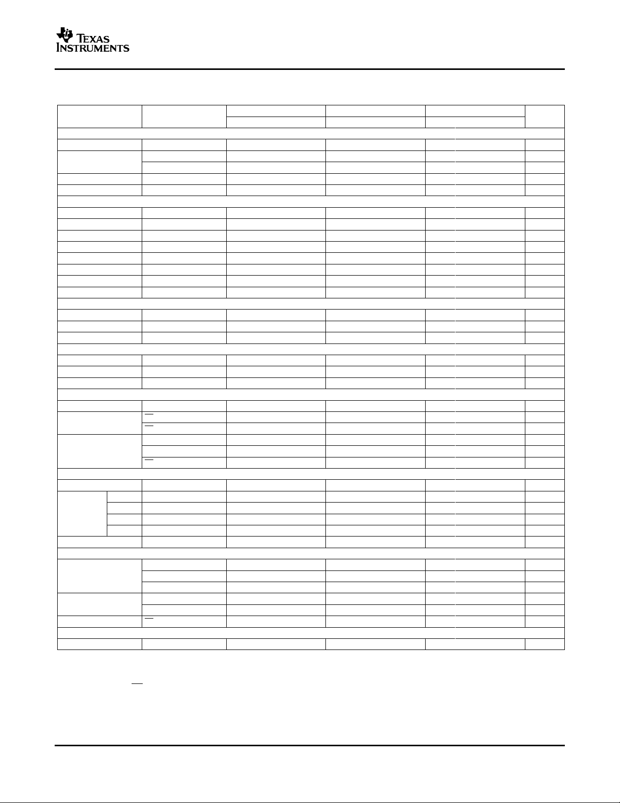
ELECTRICAL CHARACTERISTICS: +V
At –40 ° C to +85 ° C, +V
PARAMETER TEST CONDITIONS MIN TYP MAX MIN TYP MAX MIN TYP MAX UNIT
ANALOG INPUT
Full-scale input span +In – (–In) 0 V
Absolute input range
Capacitance 25 25 25 pF
Leakage current ± 1 ± 1 ± 1 µ A
SYSTEM PERFORMANCE
Resolution 12 12 12 Bits
No missing codes 11 12 11 Bits
Integral linearity error –2 ± 0.5 +2 –1 ± 0.5 +1 –0.75 ± 0.25 +0.75 LSB
Differential linearity error –2 ± 0.5 +2 –1 ± 0.5 +1 –0.75 ± 0.25 +0.75 LSB
Offset error –3 +3 –3 +3 –1 +1 LSB
Gain error –3 +3 –3 +3 –1 +1 LSB
Noise 33 33 33 µ Vrms
Power-supply rejection 82 82 82 dB
SAMPLING DYNAMICS
Conversion time 12 12 12 Clk Cycles
Acquisition time 1.5 1.5 1.5 Clk Cycles
Throughput rate 75 75 75 kHz
DYNAMIC CHARACTERISTICS
Total harmonic distortion VIN= 2.5V
SINAD VIN= 2.5V
Spurious-free dynamic range VIN= 2.5V
REFERENCE OUTPUT
Voltage range 0.05 V
Resistance
Current drain f
DIGITAL INPUT/OUTPUT
Logic family CMOS CMOS CMOS
V
IH
V
Logic levels
Data format Straight Binary Straight Binary Straight Binary
POWER-SUPPLY REQUIREMENTS
V
CC
Quienscent current
Power down CS = V
TEMPERATURE RANGE
Specified performance –40 +85 –40 +85 –40 +85 ° C
(1) LSB means least significant bit. With V
(2) The maximum clock rate of the ADS7822 is less than 1.2MHz in this power-supply range.
IL
V
OH
V
OL
= +2.7V, V
CC
+In –0.2 VCC+ 0.2 –0.2 VCC+ 0.2 –0.2 VCC+ 0.2 V
–In –0.2 +1.0 –0.2 +1.0 –0.2 +1.0 V
at 1kHz –82 –82 –82 dB
PP
at 1kHz 71 71 71 dB
PP
at 1kHz 86 86 86 dB
PP
CS = GND, f
CS = V
At code 710h 8 40 8 40 8 40 µ A
SAMPLE
CS = V
IIH= +5 µ A 2.0 5.5 2.0 5.5 2.0 5.5 V
IIL= +5 µ A –0.3 0.8 –0.3 0.8 –0.3 0.8 V
IOH= –250 µ A 2.1 2.1 2.1 V
IOL= 250 µ A 0.4 0.4 0.4 V
Specified performance 2.7 3.6 2.7 3.6 2.7 3.6 V
See Notes
See Note
f
SAMPLE
f
SAMPLE
SAMPLE
CC
= 7.5kHz 0.8 0.8 0.8 µ A
CC
(2)
and
(3)
= 7.5kHz
(5)
= 75kHz
CC
= +2.5V, f
REF
= 0Hz 5 5 5 G Ω
(3)
(4) (5)
equal to +2.5V, one LSB is 0.61mV.
REF
= +2.7V
CC
= 75kHz, and f
SAMPLE
ADS7822 ADS7822B ADS7822C
REF
CC
5 5 5 G Ω
0.001 3 0.001 3 0.001 3 µ A
2.0 2.7 2.0 2.7 2.0 2.7 V
3.6 5.25 3.6 5.25 3.6 5.25 V
20 20 20 µ A
200 325 200 325 200 325 µ A
3 3 3 µ A
= 16 × f
CLK
0 V
0.05 V
SAMPLE
, unless otherwise noted.
REF
CC
0 V
0.05 V
REF
CC
(3) See the Typical Characteristics for more information.
(4) f
(5) See the Power Dissipation section for more information regarding lower sample rates.
= 1.2MHz, CS = V
CLK
for 145 clock cycles out of every 160.
CC
V
(1)
V
Submit Documentation Feedback
3
www.ti.com
ADS7822
SBAS062B – JANUARY 1996 – REVISED MAY 2006
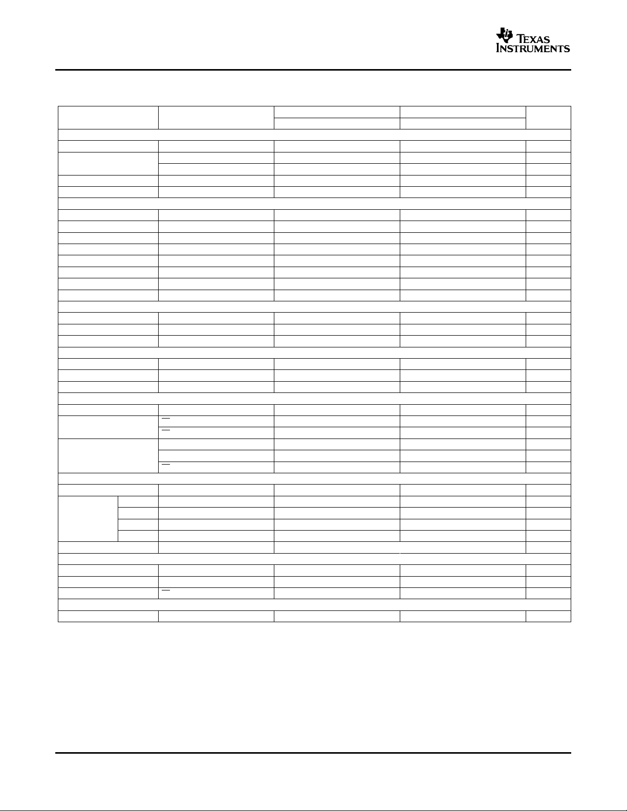
ELECTRICAL CHARACTERISTICS: +V
At –40 ° C to +85 ° C, +V
PARAMETER TEST CONDITIONS MIN TYP MAX MIN TYP MAX UNIT
ANALOG INPUT
Full-scale input span +In – (–In) 0 V
Absolute input range
Capacitance 25 25 pF
Leakage current ± 1 ± 1 µ A
SYSTEM PERFORMANCE
Resolution 12 12 Bits
No missing codes 11 12 Bits
Integral linearity error –2 +2 –1 +1 LSB
Differential linearity error ± 0.8 –1 ± 0.5 +1 LSB
Offset error –3 +3 –3 +3 LSB
Gain error –4 +4 –3 +3 LSB
Noise 33 33 µ Vrms
Power-supply rejection 70 70 dB
SAMPLING DYNAMICS
Conversion time 12 12 Clk Cycles
Acquisition time 1.5 1.5 Clk Cycles
Throughput rate 200 200 kHz
DYNAMIC CHARACTERISTICS
Total harmonic distortion VIN= 5V
SINAD VIN= 5V
Spurious-free dynamic range VIN= 5V
REFERENCE OUTPUT
Voltage range 0.05 V
Resistance
Current drain f
DIGITAL INPUT/OUTPUT
Logic family CMOS CMOS
V
IH
V
Logic levels
Data format Straight Binary Straight Binary
POWER-SUPPLY REQUIREMENTS
V
CC
Quienscent current f
Power down CS = V
TEMPERATURE RANGE
Specified performance –40 +85 –40 +85 ° C
IL
V
OH
V
OL
= +5V, V
CC
+In –0.2 VCC+ 0.2 –0.2 VCC+ 0.2 V
–In –0.2 +1.0 –0.2 +1.0 V
CS = GND, f
CS = V
CC
At code 710h 40 100 40 100 µ A
= 12.5kHz 2.5 2.5 µ A
SAMPLE
CS = V
CC
IIH= +5 µ A 3.0 5.5 3.0 5.5 V
IIL= +5 µ A –0.3 0.8 –0.3 0.8 V
IOH= –250 µ A 3.5 3.5 V
IOL= 250 µ A 0.4 0.4 V
Specified performance 4.75 5.25 4.75 5.25 V
= 200kHz 320 550 320 550 µ A
SAMPLE
CC
= +5V, f
REF
at 10kHz –78 –78 dB
PP
at 10kHz 71 71 dB
PP
at 10kHz 79 79 dB
PP
= 0Hz 5 5 G Ω
SAMPLE
CC
SAMPLE
= +5V
= 200kHz, and f
ADS7822 ADS7822B
= 16 × f
CLK
5 5 G Ω
0.001 3 0.001 3 µ A
, unless otherwise noted.
SAMPLE
REF
CC
3 3 µ A
0 V
0.05 V
REF
CC
V
(1)
V
(1) LSB means least significant bit. With V
4
equal to +5V, one LSB is 1.22mV.
REF
Submit Documentation Feedback
www.ti.com
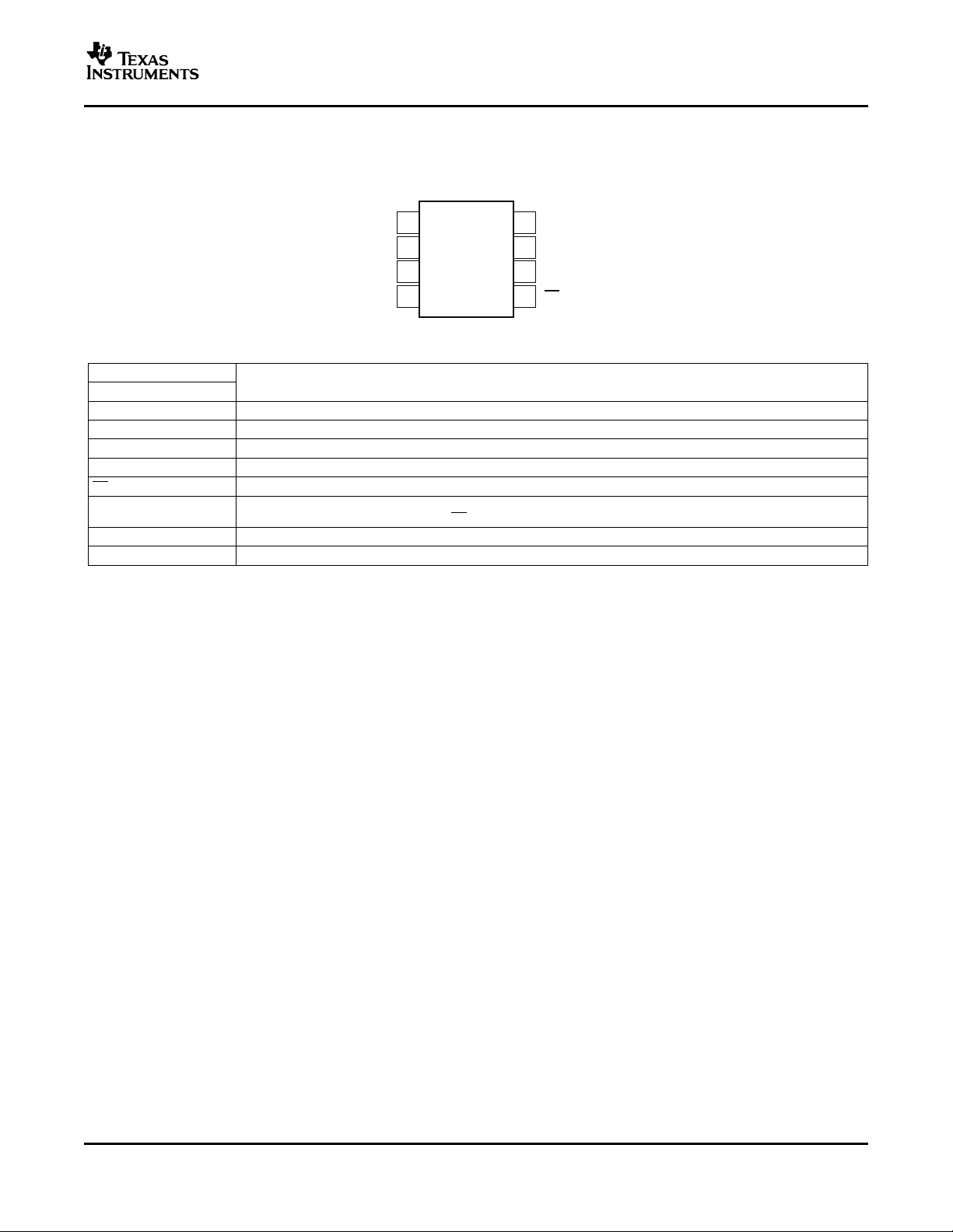
PIN CONFIGURATION
1
2
3
4
8
7
6
5
+V
CC
DCLOCK
D
OUT
CS/SHDN
V
REF
+In
-In
GND
ADS7822
D, DGK, OR P PACKAGE
SO, MSOP, or DIP
(TOP VIEW)
PIN ASSIGNMENTS
PIN
NAME NO. DESCRIPTION
V
REF
+In 2 Noninverting input
–In 3 Inverting input. Connect to ground or to remote ground sense point.
GND 4 Ground
CS/SHDN 5 Chip select when low; Shutdown mode when high.
D
OUT
DCLOCK 7 Data clock synchronizes the serial data transfer and determines conversion speed.
+V
CC
1 Reference input
The serial output data word is comprised of 12 bits of data. In operation, the data are valid on the falling edge of DCLOCK. The
6
second clock pulse after the falling edge of CS enables the serial output. After one null bit, the data are valid for the next edges.
8 Power supply
ADS7822
SBAS062B – JANUARY 1996 – REVISED MAY 2006
Submit Documentation Feedback
5
www.ti.com
1.00
0.75
0.50
0.25
0.00
-0.25
-0.50
-0.75
-1.00
IntegralLinearityError(LSB)
0 2048 4095
Code
1.00
0.75
0.50
0.25
0.00
-0.25
-0.50
-0.75
-1.00
DifferentialLinearityError(LSB)
0 2048 4095
Code
350
300
250
200
150
100
50
SupplyCurrent( A)
m
-50 -25 0 25 50 75 100
Temperature( C)°
120
100
80
60
40
20
0
SupplyCurrent(nA)
-50 -25 0 25 50 75 100
Temperature( C)°
400
350
300
250
200
150
100
QuiescentCurrent(
A)m
1 2 3 4 5
V (V)
CC
1000
100
10
1
SampleRate(kHz)
1 2 3 4 5
V (V)
CC
ADS7822
SBAS062B – JANUARY 1996 – REVISED MAY 2006
At TA= +25 ° C, V
CC
= +2.7V, V
REF
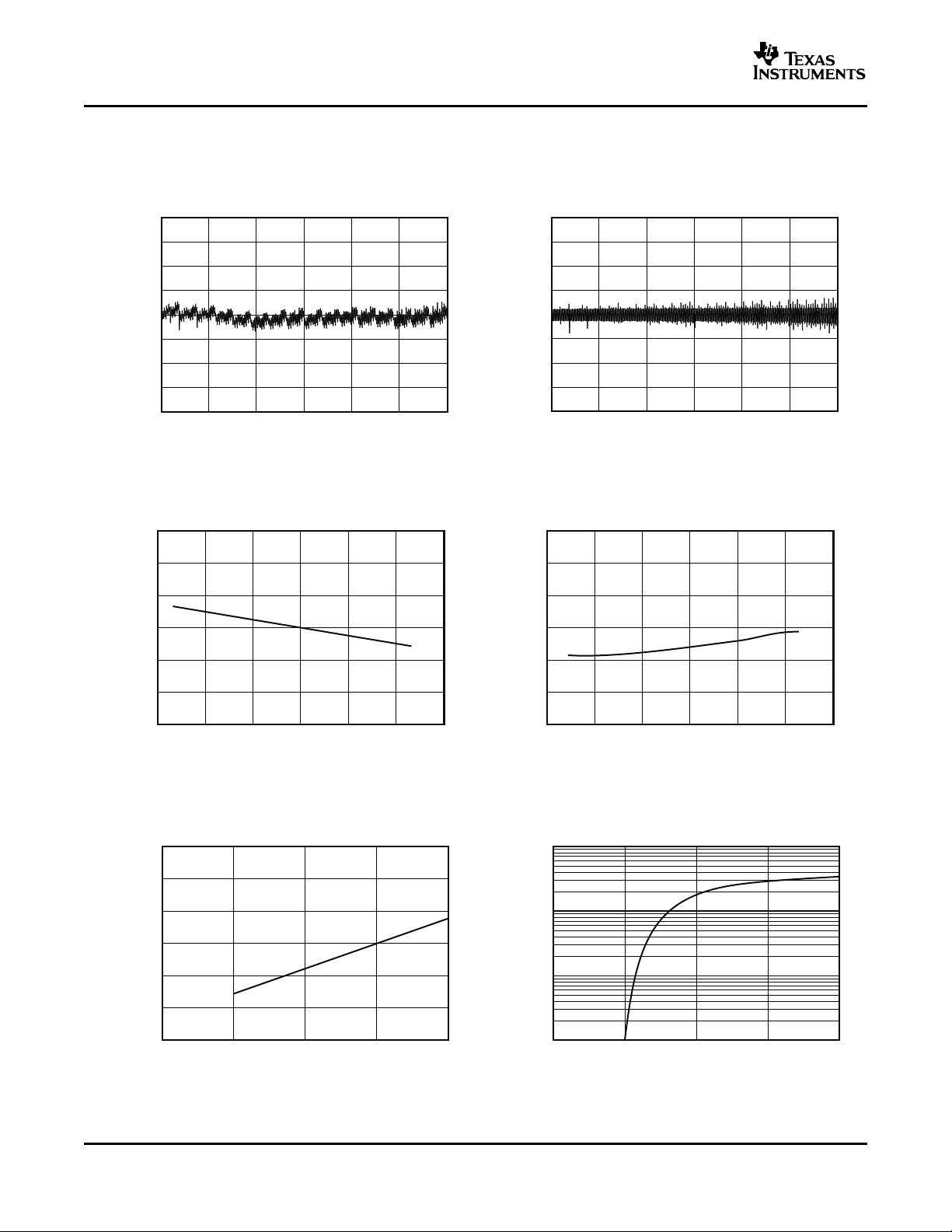
TYPICAL CHARACTERISTICS
= +2.5V, f
SAMPLE
= 75kHz, f
CLK
= 16 × f
SAMPLE
, unless otherwise specified.
INTEGRAL LINEARITY ERROR DIFFERENTIAL LINEARITY ERROR
vs CODE vs CODE
Figure 1. Figure 2.
SUPPLY CURRENT POWER-DOWN SUPPLY CURRENT
vs TEMPERATURE vs TEMPERATURE
QUIESCENT CURRENT MAXIMUM SAMPLE RATE
6
Figure 3. Figure 4.
vs V
CC
vs V
Figure 5. Figure 6.
Submit Documentation Feedback
CC
www.ti.com
1.2
1.0
0.8
0.6
0.4
0.2
0.0
-0.2
-0.4
-0.6
-0.8
ChangeinOffset(LSB)
1 2 3 4 5
ReferenceVoltage(V)
V =5V
CC
V =5V
CC
0.6
0.4
0.2
0
-0.2
-0.4
-0.6
Deltafrom25
°C(LSB)
-50
-25
0 25 50 75 100
Temperature(°C)
2.5
2.0
1.5
1.0
0.5
0.0
-0.5
-1.0
-1.5
ChangeinGain(LSB)
1 2 3 4 5
ReferenceVoltage(V)
V =5V
CC
V =5V
CC
0.15
0.10
0.05
0
-0.05
-0.10
-0.15
Deltafrom25
C(LSB)°
-50 -25 0 25 50 75 100
Temperature( C)°
12.00
11.75
11.50
11.25
11.00
10.75
10.50
10.25
10.00
EffectiveNumberofBits(rms)
0.1 1 10
ReferenceVoltage(V)
V =5V
CC
10
9
8
7
6
5
4
3
2
1
0
Peak-to-PeakNoise(LSB)
0.1 1 10
ReferenceVoltage(V)
V =5V
CC
At TA= +25 ° C, V
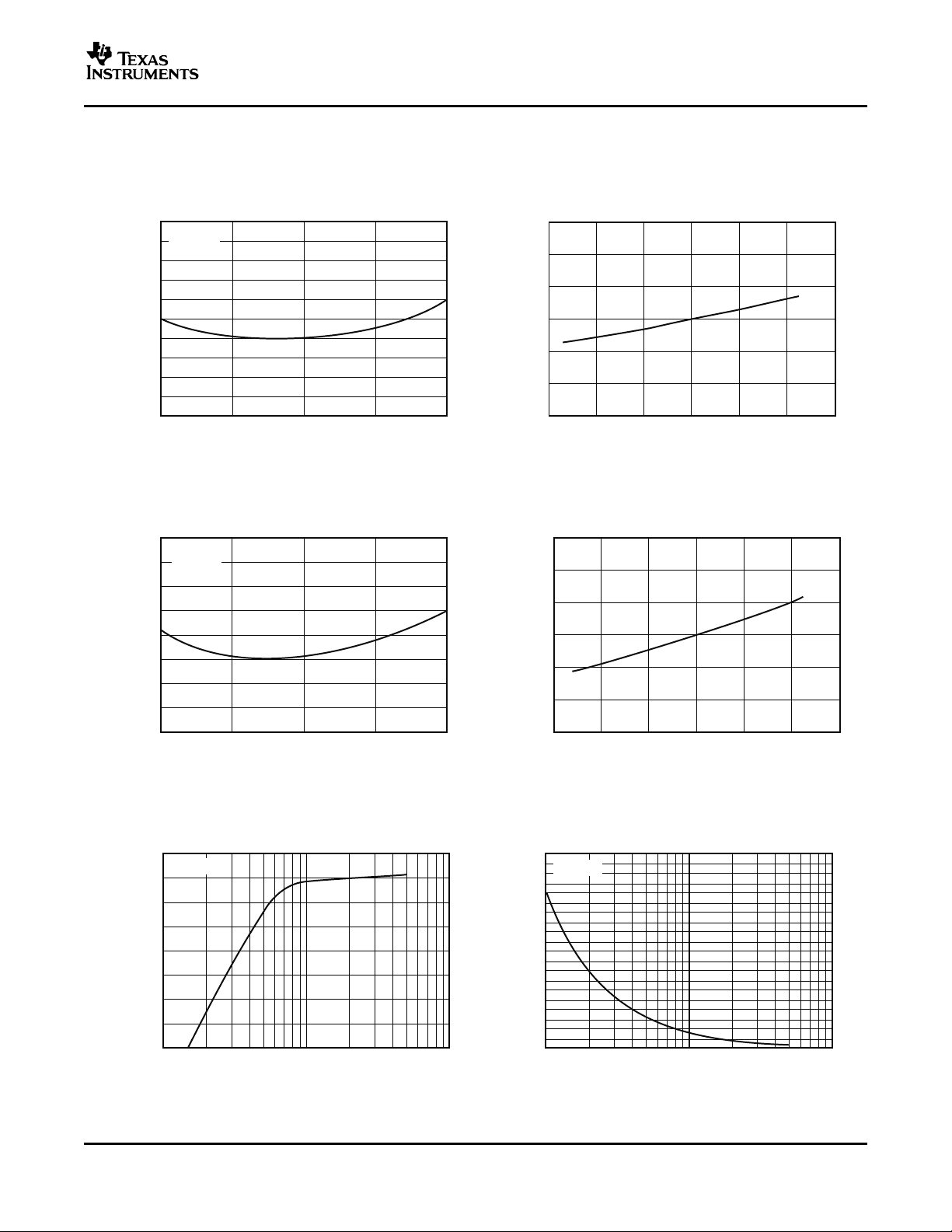
TYPICAL CHARACTERISTICS (continued)
= +2.7V, V
CC
CHANGE IN OFFSET CHANGE IN OFFSET
vs REFERENCE VOLTAGE vs TEMPERATURE
REF
= +2.5V, f
SAMPLE
= 75kHz, f
CLK
= 16 × f
SAMPLE
Figure 7. Figure 8.
ADS7822
SBAS062B – JANUARY 1996 – REVISED MAY 2006
, unless otherwise specified.
CHANGE IN GAIN CHANGE IN GAIN
vs REFERENCE VOLTAGE vs TEMPERATURE
Figure 9. Figure 10.
EFFECTIVE NUMBER OF BITS PEAK-TO-PEAK NOISE
vs REFERENCE VOLTAGE vs REFERENCE VOLTAGE
Figure 11. Figure 12.
Submit Documentation Feedback
7
 Loading...