

AD
S7807
A
D
S
7
8
0
7
SBAS022B – NOVEMBER 1992 – REVISED SEPTEMBER 2003
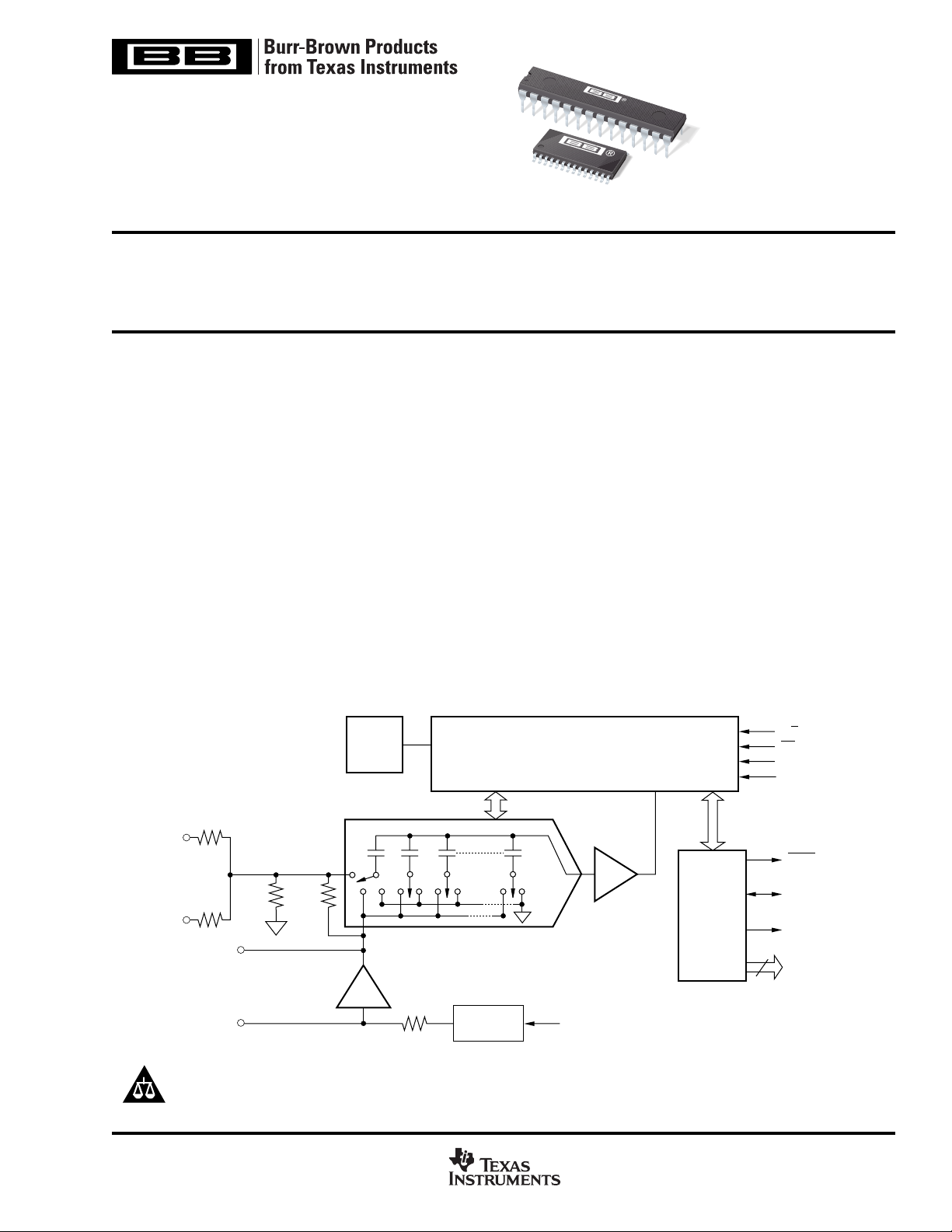
Low-Power, 16-Bit, Sampling CMOS
ANALOG-to-DIGITAL CONVERTER
ADS7807
FEATURES
● 35mW max POWER DISSIPATION
● 50µW POWER-DOWN MODE
● 25µs max ACQUISITION AND CONVERSION
● ±1.5LSB max INL
● DNL: 16 bits “No Missing Codes”
● 86dB min SINAD WITH 1kHz INPUT
●±10V, 0V TO +5V, AND 0V TO +4V INPUT RANGES
● SINGLE +5V SUPPLY OPERATION
● PARALLEL AND SERIAL DATA OUTPUT
● PIN-COMPATIBLE WITH THE 12-BIT ADS7806
● USES INTERNAL OR EXTERNAL REFERENCE
● 0.3" DIP-28 AND SO-28
R1
R2
Clock
40kΩ
IN
20kΩ
10kΩ
IN
CAP
40kΩ
Buffer
Successive Approximation Register and Control Logic
CDAC
DESCRIPTION
The ADS7807 is a low-power, 16-bit, sampling Analog-toDigital (A/D) converter using state-of-the-art CMOS structures. It contains a complete 16-bit, capacitor-based, Successive Approximation Register (SAR) A/D converter with
sample-and-hold, clock, reference, and microprocessor interface with parallel and serial output drivers.
The ADS7807 can acquire and convert 16-bits to within
±1.5LSB in 25µs max while consuming only 35mW max.
Laser trimmed scaling resistors provide standard industrial
input ranges of ±10V and 0V to +5V. In addition, a 0V to +4V
range allows development of complete single-supply systems.
The ADS7807 is available in a 0.3" DIP-28 and SO-28, both
fully specified for operation over the industrial –40°C to
+85°C temperature range.
R/C
CS
BYTE
Power
Down
BUSY
Comparator
Parallel
and
Serial
Data
Out
Serial Data
Clock
Serial Data
Parallel Data
8
REF
Please be aware that an important notice concerning availability, standard warranty, and use in critical applications of
Texas Instruments semiconductor products and disclaimers thereto appears at the end of this data sheet.
All trademarks are the property of their respective owners.
PRODUCTION DATA information is current as of publication date.
Products conform to specifications per the terms of Texas Instruments
standard warranty. Production processing does not necessarily include
testing of all parameters.
6kΩ
Internal
+2.5V Ref
www.ti.com
Reference
Power-Down
Copyright © 1992-2003, Texas Instruments Incorporated
ABSOLUTE MAXIMUM RATINGS
Analog Inputs: R1IN........................................................................... ±12V
Ground Voltage Differences: DGND, AGND1, and AGND2 ............. ±0.3V
V
ANA
V
to V
DIG
V
........................................................................................................ 7V
DIG
Digital Inputs ............................................................. –0.3V to V
Maximum Junction Temperature ................................................... +165°C
Internal Power Dissipation ............................................................. 825mW
Lead Temperature (soldering, 10s) ............................................... +300°C
NOTE: (1) Stresses above those listed under “Absolute Maximum Ratings”
may cause permanent damage to the device. Exposure to absolute maximum
conditions for extended periods may affect device reliability.
R2
.......................................................................... ±5.5V
IN
CAP .................................. V
REF .........................................Indefinite Short to AGND2,
....................................................................................................... 7V
...................................................................................... +0.3V
ANA
(1)
+ 0.3V to AGND2 – 0.3V
ANA
Momentary Short to V
DIG
ANA
+ 0.3V
ELECTROSTATIC
DISCHARGE SENSITIVITY
This integrated circuit can be damaged by ESD. Texas Instruments recommends that all integrated circuits be handled with
appropriate precautions. Failure to observe proper handling
and installation procedures can cause damage.
ESD damage can range from subtle performance degradation to complete device failure. Precision integrated circuits
may be more susceptible to damage because very small
parametric changes could cause the device not to meet its
published specifications.
PACKAGE/ORDERING INFORMATION
MAXIMUM SPECIFIED SIGNAL-TOINTEGRAL NO MISSING (NOISE + SPECIFIED
LINEARITY CODE LEVEL DISTORTION) PACKAGE TEMPERATURE PACKAGE ORDERING TRANSPORT
PRODUCT ERROR (LSB) (LSB) RATIO (DB) PACKAGE-LEAD DESIGNATOR
ADS7807P ±31583Dip-28NT–40°C to +85°C ADS7807P ADS7807P Tubes, 13
ADS7807PB ±1.5 16 86
ADS7807U ±3 15 83 SO-28 DW –40°C to +85°C ADS7807U ADS7807U Tubes, 28
" " " " " " " " ADS7807U/1K Tape and Reel, 1000
ADS7807UB ±1.5 16 86
" " " " " " " " ADS7807UB/1K Tape and Reel, 1000
NOTE: (1) For the most current specifications and package information, refer to our web site at www.ti.com.
MINIMUM
(1)
RANGE MARKING NUMBER MEDIA, QUANTITY
"""ADS7807PB ADS7807PB Tubes, 13
"""ADS7807UB ADS7807UB Tubes, 28
ELECTRICAL CHARACTERISTICS
At TA = –40°C to +85°C, fS = 40kHz, V
PARAMETER CONDITIONS MIN TYP MAX MIN TYP MAX UNITS
RESOLUTION 16 ✻ Bits
ANALOG INPUT
Voltage Ranges ±10, 0 to +5, 0 to +4 V
Impedance (See Table II)
Capacitance 35 ✻ pF
THROUGHPUT SPEED
Conversion Time 20 ✻ µs
Complete Cycle Acquire and Convert 25 ✻ µs
Throughput Rate 40 ✻ kHz
DC ACCURACY
Integral Linearity Error ±3 ±1.5 LSB
Differential Linearity Error +3, –2 +1.5, –1LSB
No Missing Codes 15 16 Bits
Transition Noise
Gain Error ±0.2 ±0.1 %
Full-Scale Error
Full-Scale Error Drift ±7 ±5 ppm/°C
Full-Scale Error
Full-Scale Error Drift Ext. 2.5000V Ref ±0.5 ✻ ppm/°C
Bipolar Zero Error
Bipolar Zero Error Drift ±10V Range ±0.5 ✻ ppm/°C
Unipolar Zero Error
Unipolar Zero Error Drift 0V to 5V, 0V to 4V Ranges ±0.5 ✻ ppm/°C
Recovery Time to Rated Accuracy 2.2µF Capacitor to CAP 1 ✻ ms
from Power-Down
Power-Supply Sensitivity +4.75V < VS < +5.25V ±8 ✻ LSB
(V
DIG
= V
ANA
(2)
(3,4)
(3,4)
(3)
(3)
(5)
= VS)
= V
DIG
= +5V, and using internal reference and fixed resistors (see Figure 7b), unless otherwise specified.
ANA
ADS7807P, U ADS7807PB, UB
0.8 ✻ LSB
±0.5 ±0.25 %
Ext. 2.5000V Ref ±0.5 ±0.25 %
±10V Range ±10 ✻ mV
0V to 5V, 0V to 4V Ranges ±3 ✻ mV
(1)
2
www.ti.com
ADS7807
SBAS022B
ELECTRICAL CHARACTERISTICS (Cont.)
At TA = –40°C to +85°C, fS = 40kHz, V
PARAMETER CONDITIONS MIN TYP MAX MIN TYP MAX UNITS
AC ACCURACY
Spurious-Free Dynamic Range f
Total Harmonic Distortion f
Signal-to-(Noise + Distortion) f
Signal-to-Noise f
Usable Bandwidth
(7)
Full-Power Bandwidth (–3dB) 600 ✻ kHz
SAMPLING DYNAMICS
Aperture Delay 40 ✻ ns
Aperture Jitter 20 ✻ ps
Transient Response FS Step 5 ✻ µs
Over-Voltage Recovery
(8)
REFERENCE
Internal Reference Voltage No Load 2.48 2.5 2.52 ✻✻✻ V
Internal Reference Source Current 1 ✻ µA
(Must use external buffer.)
Internal Reference Drift 8 ✻ ppm/°C
External Reference Voltage Range 2.3 2.5 2.7 ✻✻ ✻ V
for Specified Linearity
External Reference Current Drain External 2.5000V Ref 100 ✻ µA
DIGITAL INPUTS
Logic Levels
V
IL
(9)
V
IH
I
IL
I
IH
DIGITAL OUTPUTS Parallel 16 bits in 2-bytes; Serial
Data Format Binary Two’s Complement or Straight Binary
Data Coding
V
OL
V
OH
Leakage Current High-Z State, ±5 ✻ µA
Output Capacitance High-Z State 15 ✻ pF
DIGITAL TIMING
Bus Access Time R
Bus Relinquish Time R
POWER SUPPLIES
Specified Performance
V
DIG
V
ANA
I
DIG
I
ANA
Power Dissipation V
TEMPERATURE RANGE
Specified Performance –40 +85 ✻✻ °C
Derated Performance –55 +125 ✻✻ °C
Storage –65 +150 ✻✻ °C
Thermal Resistance (
DIP 75 ✻ °C/W
θ
)
JA
SO 75 ✻ °C/W
✻ Same specifications as ADS7807P, U.
NOTES: (1) LSB means Least Significant Bit. One LSB for the ±10V input range is 305µV. (2) Typical rms noise at worst-case transition. (3) As measured with
fixed resistors, see Figure 7b. Adjustable to zero with external potentiometer. (4) Full-scale error is the worst case of –Full-Scale or +Full-Scale untrimmed deviation
from ideal first and last code transitions, divided by the transition voltage (not divided by the full-scale range) and includes the effect of offset error. (5) This is the
time delay after the ADS7807 is brought out of Power-Down mode until all internal settling occurs and the analog input is acquired to rated accuracy. A Convert
command after this delay will yield accurate results. (6) All specifications in dB are referred to a full-scale input. (7) Usable bandwidth defined as full-scale input
frequency at which Signal-to-(Noise + Distortion) degrades to 60dB. (8) Recovers to specified performance after 2 • FS input overvoltage. (9) The minimum V
level for the DATACLK signal is 3V.
= V
DIG
= +5V, and using internal reference and fixed resistors (see Figure 7b), unless otherwise specified.
ANA
ADS7807P, U ADS7807PB, UB
= 1kHz, ±10V 90 100 96 ✻ dB
IN
= 1kHz, ±10V –100 –90 ✻ –96 dB
IN
= 1kHz, ±10V 83 88 86 ✻ dB
IN
–60dB Input 30 32 dB
= 1kHz, ±10V 83 88 86 ✻ dB
IN
130 ✻ kHz
750 ✻ ns
–0.3 +0.8 ✻✻V
+2.0 VD + 0.3V ✻✻V
VIL = 0V ±10 ✻ µA
VIH = 5V ±10 ✻ µA
I
= 1.6mA +0.4 ✻ V
SINK
I
= 500µA+4 ✻ V
SOURCE
V
= 0V to V
OUT
= 3.3kΩ, CL = 50pF 83 ✻ ns
L
= 3.3kΩ, CL = 10pF 83 ✻ ns
L
Must be ≤ V
ANA
DIG
+4.75 +5 +5.25 ✻✻✻ V
+4.75 +5 +5.25 ✻✻✻ V
0.6 ✻ mA
5.0 ✻ mA
= V
ANA
= 5V, fS = 40kHz 28 35 ✻✻mW
DIG
REFD HIGH 23 ✻ mW
PWRD and REFD HIGH 50 ✻ µW
(6)
IH
ADS7807
SBAS022B
www.ti.com
3
PIN DESCRIPTIONS
ANA
DIG
DIGITAL
IN
IN
Analog Input. See Figure 7.
Analog Input. See Figure 7.
unconnected when using serial output.
enables the parallel output.
falling edge will start the transmission of serial data results from the previous conversion.
have been updated.
Analog Supply. Nominally +5V. Decouple with 0.1µF ceramic and 10µF tantalum capacitors.
Digital Supply. Nominally +5V. Connect directly to pin 27. Must be ≤ V
ANA
.
PIN # NAME I/O DESCRIPTION
1R1
2 AGND1 Analog Sense Ground.
3R2
4 CAP Reference Buffer Output. 2.2µF tantalum capacitor to ground.
5 REF Reference Input/Output. 2.2µF tantalum capacitor to ground.
6 AGND2 Analog Ground
7 SB/BTC I Selects Straight Binary or Binary Two’s Complement for Output Data Format.
8 EXT/INT I External/Internal data clock select.
9 D7 O Data Bit 7 if BYTE is HIGH. Data bit 15 (MSB) if BYTE is LOW. Hi-Z when CS is HIGH and/or R/C is LOW. Leave
10 D6 O Data Bit 6 if BYTE is HIGH. Data bit 14 if BYTE is LOW. Hi-Z when CS is HIGH and/or R/C is LOW.
11 D5 O Data Bit 5 if BYTE is HIGH. Data bit 13 if BYTE is LOW. Hi-Z when CS is HIGH and/or R/C is LOW.
12 D4 O Data Bit 4 if BYTE is HIGH. Data bit 12 if BYTE is LOW. Hi-Z when CS is HIGH and/or R/C is LOW.
13 D3 O Data Bit 3 if BYTE is HIGH. Data bit 11 if BYTE is LOW. Hi-Z when CS is HIGH and/or R/C is LOW.
14 DGND Digital Ground
15 D2 O Data Bit 2 if BYTE is HIGH. Data bit 10 if BYTE is LOW. Hi-Z when CS is HIGH and/or R/C is LOW.
16 D1 O Data Bit 1 if BYTE is HIGH. Data bit 9 if BYTE is LOW. Hi-Z when CS is HIGH and/or R/C is LOW.
17 D0 O Data Bit 0 (LSB) if BYTE is HIGH. Data bit 8 if BYTE is LOW. Hi-Z when CS is HIGH and/or R/C is LOW.
18 DATACLK I/O Data Clock Output when EXT/INT is LOW. Data clock input when EXT/INT is HIGH.
19 SDATA O Serial Output Synchronized to DATACLK
20 TAG I Serial Input When Using an External Data Clock
21 BYTE I Selects 8 most significant bits (LOW) or 8 least significant bits (HIGH) on parallel output pins.
22 R/C I With CS LOW and BUSY HIGH, a Falling Edge on R/C Initiates a New Conversion. With CS LOW, a rising edge on R/C
23 CS I Internally OR’d with R/C. If R/C is LOW, a falling edge on CS initiates a new conversion. If EXT/INT is LOW, this same
24 BUSY O At the start of a conversion, BUSY goes LOW and stays LOW until the conversion is completed and the digital outputs
25 PWRD I PWRD HIGH shuts down all analog circuitry except the reference. Digital circuitry remains active.
26 REFD I REFD HIGH shuts down the internal reference. External reference will be required for conversions.
27 V
28 V
PIN CONFIGURATION
Top View DIP, SO
R1
AGND1
R2
CAP
REF
AGND2
SB/BTC
EXT/INT
D7
D6
D5
D4
D3
DGND
1
IN
2
3
IN
4
5
6
7
ADS7807
8
9
10
11
12
13
14
28
27
26
25
24
23
22
21
20
19
18
17
16
15
V
DIG
V
ANA
REFD
PWRD
BUSY
CS
R/C
BYTE
TAG
SDATA
DATACLK
D0
D1
D2
ANALOG CONNECT R1INCONNECT R2
INPUT VIA 200Ω VIA 100Ω
IN
RANGE TO TO IMPEDANCE
±10V V
0V to 5V AGND V
0V to 4V V
IN
IN
CAP 45.7kΩ
IN
V
IN
20.0kΩ
21.4kΩ
TABLE I. Input Range Connections. See Figure 7.
4
www.ti.com
ADS7807
SBAS022B
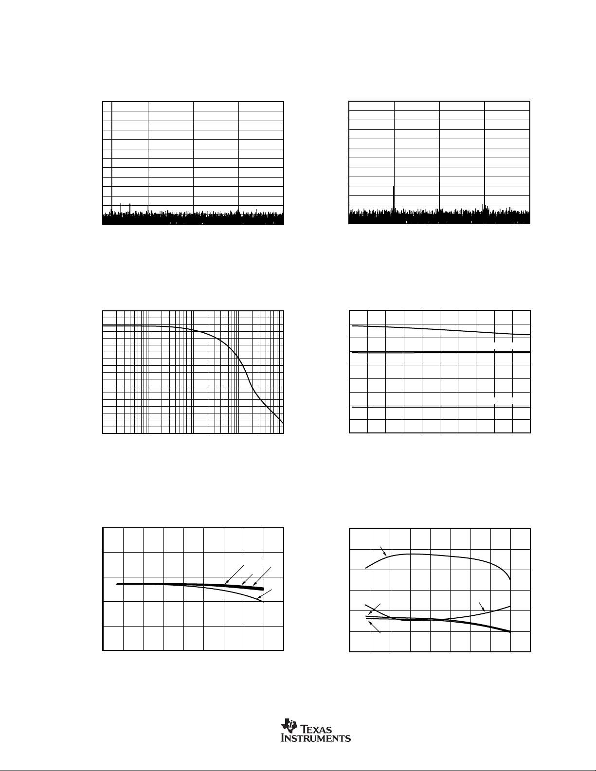
TYPICAL CHARACTERISTICS
SIGNAL-TO-(NOISE + DISTORTION)
vs INPUT FREQUENCY AND INPUT AMPLITUDE
Input Signal Frequency (kHz)
02468101214161820
100
80
90
70
60
50
40
30
20
10
SINAD (dB)
0dB
–20dB
–60dB
AC PARAMETERS vs TEMPERATURE
(f
IN
= 1kHz, 0dB)
SFDR
THD
Temperature (°C)
–75 –50 –25 0 25 50 75 100 125 150
110
105
100
95
90
85
80
–80
–85
–90
–95
–100
–105
–110
SFDR, SINAD, and SNR (dB)
THD (dB)
SNR
SINAD
At TA = +25°C, fS = 40kHz, V
DIG
= V
= +5V, and using internal reference and fixed resistors (see Figure 7b), unless otherwise specified.
ANA
FREQUENCY SPECTRUM
0
–10
–20
–30
–40
–50
–60
–70
–80
Amplitude (dB)
–90
–100
–110
–120
–130
0 5 10 15 20
100
90
80
70
60
50
SINAD (dB)
40
30
20
10
100 1k 10k 100k 1M
(8192 Point FFT; f
Frequency (kHz)
SIGNAL-TO-(NOISE + DISTORTION)
vs INPUT FREQUENCY (f
Input Signal Frequency (Hz)
= 1kHz, 0dB)
IN
= 0dB)
IN
FREQUENCY SPECTRUM
0
–10
–20
–30
–40
–50
–60
–70
–80
Amplitude (dB)
–90
–100
–110
–120
–130
0 5 10 15 20
(8192 Point FFT; f
Frequency (kHz)
= 15kHz, 0dB)
IN
SIGNAL-TO-(NOISE + DISTORTION) vs TEMPERATURE
100
95
90
85
SINAD (dB)
80
75
–75 –50 –25 0 25 50 75 100 125 150
ADS7807
SBAS022B
(f
= 1kHz, 0dB; fS = 10kHz to 40kHz)
IN
Temperature (°C)
10kHz
20kHz
30kHz
40kHz
www.ti.com
5
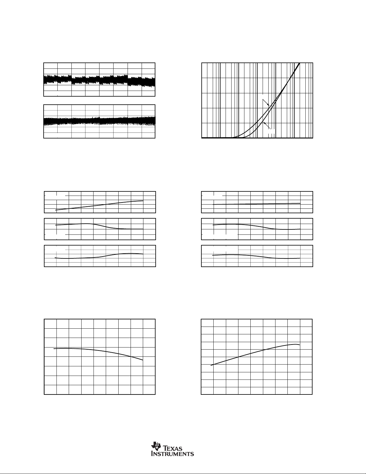
TYPICAL CHARACTERISTICS (Cont.)
At TA = +25°C, fS = 40kHz, V
3
2
1
0
–1
16-Bit (LSBs)16-Bit (LSBs)
–2
All Codes INL
–3
3
2
1
0
–1
–2
All Codes DNL
–3
0 8192 16384 24576 32768
DIG
= V
= +5V, and using internal reference and fixed resistors (see Figure 7b), unless otherwise specified.
ANA
40960 49152 57344 65535
Decimal Code
POWER-SUPPLY RIPPLE SENSITIVITY
INL/DNL DEGRADATION PER LSB OF P-P RIPPLE
1
–1
10
–2
10
–3
10
–4
10
Linearity Degradation (LSB/LSB)
–5
10
1
10
2
10
3
10
Power-Supply Ripple Frequency (Hz)
INL
DNL
4
10
5
10
6
10
7
10
3
2
BPZ Error
1
0
–1
–2
mV From Ideal
0.20
0
ENDPOINT ERRORS (20V Bipolar Range)
Percent
From Ideal
–0.20
0.20
+F
–F
Error
S
Error
S
0
Percent
From Ideal
–0.20
–75 –50 –25 0 25
50 75 100 125 150
Temperature (°C)
INTERNAL REFERENCE VOLTAGE vs TEMPERATURE
2.520
2.515
2.510
2.505
2.500
2.495
Internal Reference (V)
2.490
2.485
2.480
–75 –50 –25 0 25 50 75 100 125 150
Temperature (°C)
3
2
UPO Error
1
0
–1
–2
mV From Ideal
0.40
0.20
ENDPOINT ERRORS (Unipolar Ranges)
Percent
Percent
+F
From Ideal
0.40
0.20
From Ideal
Error (4V Range)
S
0
–F
Error (5V Range)
S
0
–75 –50 –25 0 25
50 75 100 125 150
Temperature (°C)
CONVERSION TIME vs TEMPERATURE
19.4
19.2
19
18.8
Conversion Time (µs)
18.6
–75 –50 –25 0 25 50 75 100 125 150
Temperature (°C)
6
www.ti.com
ADS7807
SBAS022B
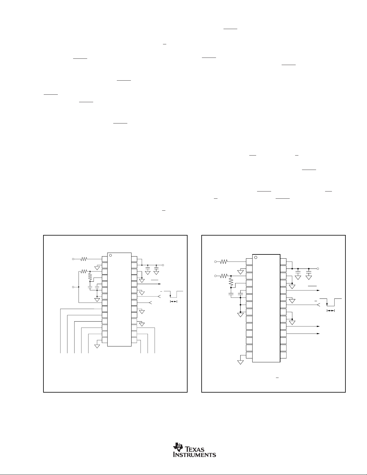
BASIC OPERATION
PARALLEL OUTPUT
Figure 1a shows a basic circuit to operate the ADS7807 with
a ±10V input range and parallel output. Taking
LOW for a minimum of 40ns (12µs max) will initiate a
conversion.
BUSY
(pin 24) will go LOW and stay LOW until
the conversion is completed and the output register is updated. If BYTE (pin 21) is LOW, the eight Most Significant
Bits (MSBs) will be valid when
BUSY
rises; if BYTE is HIGH,
the eight Least Significant Bits (LSBs) will be valid when
BUSY
rises. Data will be output in Binary Two’s Complement
(BTC) format.
BUSY
going HIGH can be used to latch the
data. After the first byte has been read, BYTE can be toggled
allowing the remaining byte to be read. All convert commands will be ignored while
BUSY
is LOW.
The ADS7807 will begin tracking the input signal at the end
of the conversion. Allowing 25µs between convert commands assures accurate acquisition of a new signal.
The offset and gain are adjusted internally to allow external
trimming with a single supply. The external resistors compensate for this adjustment and can be left out if the offset and gain
will be corrected in software (refer to the Calibration section).
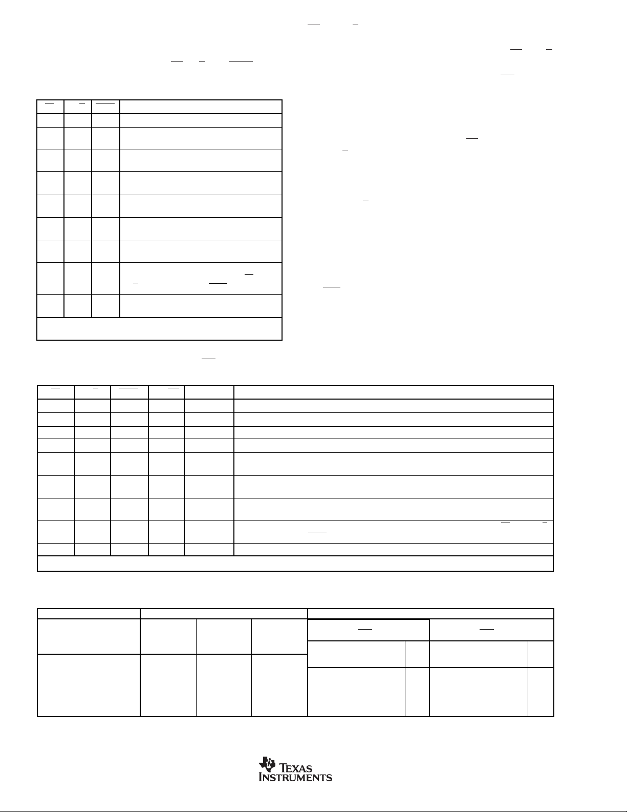
SERIAL OUTPUT
Figure 1b shows a basic circuit to operate the ADS7807 with
a ±10V input range and serial output. Taking
LOW for 40ns (12µs max) will initiate a conversion and
R/C
R/C
(pin 22)
(pin 22)
output valid data from the previous conversion on SDATA
(pin 19) synchronized to 16 clock pulses output on DATACLK
(pin 18).
BUSY
(pin 24) will go LOW and stay LOW until the
conversion is completed and the serial data has been transmitted. Data will be output in BTC format, MSB first, and will
be valid on both the rising and falling edges of the data clock.
BUSY
going HIGH can be used to latch the data. All convert
commands will be ignored while
BUSY
is LOW.
The ADS7807 will begin tracking the input signal at the end
of the conversion. Allowing 25µs between convert commands assures accurate acquisition of a new signal.
The offset and gain are adjusted internally to allow external
trimming with a single supply. The external resistors compensate for this adjustment and can be left out if the offset and
gain will be corrected in software (refer to the Calibration
section).
STARTING A CONVERSION
The combination of CS (pin 23) and
minimum of 40ns puts the sample-and-hold of the ADS7807
in the hold state and starts conversion ‘n’.
go LOW and stay LOW until conversion ‘n’ is completed and
the internal output register has been updated. All new convert commands during
or
R/C
must go HIGH before
BUSY
LOW will be ignored. CS and/
conversion will be initiated without sufficient time to acquire
a new signal.
R/C
(pin 22) LOW for a
BUSY
BUSY
goes HIGH, or a new
(pin 24) will
Parallel Output
200Ω
Pin 21
LOW
HIGH
±10V
+5V
B14 B11
(MSB)
B6 B3
66.5kΩ
2.2µF
B13 B12B15
B5 B4B7Pin 21
100Ω
2.2µF
++
1
2
3
4
5
6
7
ADS7807
8
9
10
11
12
13
14
28
27
26
25
24
23
22
21
20
19
18
17
16
15
B10 B9 B8
0.1µF
+
BUSY
BYTE
(1)
NC
B2 B1 B0
(LSB)
10µF
+
R/C
+5V
Convert Pulse
40ns min
NOTE: (1) SDATA (pin 19) is always active.
FIGURE 1a. Basic ±10V Operation, both Parallel and Serial
Output.
Serial Output
200Ω
±10V
+5V
66.5kΩ
2.2µF
100Ω
2.2µF
++
(1)
NC
(1)
NC
(1)
NC
(1)
NC
(1)
NC
1
2
3
4
5
6
7
ADS7807
8
9
10
11
12
13
14
28
0.1µF
10µF
27
+
26
25
24
23
22
21
20
19
18
17
16
15
DATACLK
(1)
NC
(1)
NC
(1)
NC
+
BUSY
SDATA
+5V
Convert Pulse
R/C
40ns min
NOTE: (1) These pins should be left unconnected.
They will be active when
R/C
is HIGH.
FIGURE 1b. Basic ±10V Operation with Serial Output.
ADS7807
SBAS022B
www.ti.com
7
The ADS7807 will begin tracking the input signal at the end
of the conversion. Allowing 25µs between convert commands assures accurate acquisition of a new signal. Refer to
Tables II and III for a summary of
CS, R/C
, and
BUSY
states,
and Figures 2 through 6 for timing diagrams.
CS R/C BUSY OPERATION
1 X X None. Databus is in Hi-Z state.
↓ 0 1 Initiates conversion ‘n’. Databus remains
0 ↓ 1 Initiates conversion ‘n’. Databus enters Hi-Z
01↑ Conversion ‘n’ completed. Valid data from
↓ 1 1 Enables databus with valid data from
↓ 1 0 Enables databus with valid data from
0 ↑ 0 Enables databus with valid data from
00↑ New conversion initiated without acquisition
X X 0 New convert commands ignored. Conversion
NOTE: (1) See Figures 2 and 3 for constraints on data valid from
conversion ‘n – 1’.
in Hi-Z state.
state.
conversion ‘n’ on the databus.
conversion ‘n’.
conversion ‘n – 1’
conversion ‘n – 1’
of a new signal. Data will be invalid. CS and/or
R/C must be HIGH when BUSY goes HIGH.
‘n’ in progress.
(1)
. Conversion n in progress.
(1)
. Conversion ‘n’ in progress.
TABLE III. Control Functions When Using Parallel Output
(DATACLK tied LOW,
EXT/INT
tied HIGH).
CS
and
R/C
are internally OR’ed and level triggered. There
is not a requirement which input goes LOW first when
initiating a conversion. If, however, it is critical that
CS
or
R/C
initiates conversion ‘n’, be sure the less critical input is LOW
at least 10ns prior to the initiating input. If
EXT/INT
(pin 8) is
LOW when initiating conversion ‘n’, serial data from conversion ‘n – 1’ will be output on SDATA (pin 19) following the
start of conversion ‘n’. See Internal Data Clock in the Reading Data section.
To reduce the number of control pins,
using
R/C
to control the read and convert modes. This will
CS
can be tied LOW
have no effect when using the internal data clock in the serial
output mode. The parallel output and the serial output (only
when using an external data clock), however, will be affected
whenever
R/C
goes HIGH. Refer to the Reading Data
section.
READING DATA
The ADS7807 outputs serial or parallel data in Straight Binary
(SB) or Binary Two’s Complement data output format. If
SB/BTC
if LOW, the output will be in BTC format. Refer to Table IV for
ideal output codes.
The parallel output can be read without affecting the internal
output registers; however, reading the data through the serial
port will shift the internal output registers one bit per data
(pin 7) is HIGH, the output will be in SB format, and
CS R/C BUSY EXT/INT DATACLK OPERATION
↓ 0 1 0 Output Initiates conversion ‘n’. Valid data from conversion ‘n – 1’ clocked out on SDATA.
0 ↓ 1 0 Output Initiates conversion ‘n’. Valid data from conversion ‘n – 1’ clocked out on SDATA.
↓ 0 1 1 Input Initiates conversion ‘n’. Internal clock still runs conversion process.
0 ↓ 1 1 Input Initiates conversion ‘n’. Internal clock still runs conversion process.
↓ 1 1 1 Input Conversion ‘n’ completed. Valid data from conversion ‘n’ clocked out on SDATA synchronized
↓ 1 0 1 Input Valid data from conversion ‘n – 1’ output on SDATA synchronized to external data clock.
0 ↑ 0 1 Input Valid data from conversion ‘n – 1’ output on SDATA synchronized to external data clock.
00↑ X X New conversion initiated without acquisition of a new signal. Data will be invalid. CS and/or R/C
X X 0 X X New convert commands ignored. Conversion ‘n’ in progress.
NOTE: (1) See Figures 4, 5, and 6 for constraints on data valid from conversion “n-1”.
to external data clock.
Conversion ‘n’ in progress.
Conversion ‘n’ in progress.
must be HIGH when BUSY goes HIGH.
TABLE III. Control Functions When Using Serial Output.
DESCRIPTION ANALOG INPUT
Full-Scale Range ±10 0V to 5V 0V to 4V
Least Significant Bit (LSB) 305µV76µV61µV
+Full-Scale (FS – 1LSB) 9.999695V 4.999924V 3.999939V 0111 1111 1111 1111 7FFF 1111 1111 1111 1111 FFFF
Midscale 0V 2.5V 2V 0000 0000 0000 0000 0000 1000 0000 0000 0000 8000
One LSB Below Midscale –305µV 2.499924V 1.999939V 1111 1111 1111 1111 FFFF 0111 1111 1111 1111 7FFF
–Full-Scale –10V 0V 0V 1000 0000 0000 0000 8000 0000 0000 0000 0000 0000
BINARY TWO’S COMPLEMENT STRAIGHT BINARY
(SB/BTC LOW) (SB/BTC HIGH)
BINARY CODE CODE BINARY CODE CODE
DIGITAL OUTPUT
HEX HEX
TABLE IV. Output Codes and Ideal Input Voltages.
8
www.ti.com
ADS7807
SBAS022B

clock pulse. As a result, data can be read on the parallel port
prior to reading the same data on the serial port, but data
cannot be read through the serial port prior to reading the
same data on the parallel port.
PARALLEL OUTPUT
To use the parallel output, tie
DATACLK (pin 18) LOW. SDATA (pin 19) should be left
unconnected. The parallel output will be active when
22) is HIGH and
of
CS
and
CS
(pin 23) is LOW. Any other combination
R/C
will tri-state the parallel output. Valid conversion data can be read in two 8-bit bytes on D7-D0 (pins 9-13
and 15-17). When BYTE (pin 21) is LOW, the 8 most significant bits will be valid with the MSB on D7. When BYTE is
HIGH, the 8 least significant bits will be valid with the LSB on
D0. BYTE can be toggled to read both bytes within one
conversion cycle.
Upon initial power up, the parallel output will contain indeterminate data.
EXT/INT
(pin 8) HIGH and
R/C
(pin
PARALLEL OUTPUT (AFTER A CONVERSION)
After conversion ‘n’ is completed and the output registers
have been updated,
BUSY
(pin 24) will go HIGH. Valid data
from conversion ‘n’ will be available on D7-D0 (pins 9-13 and
15-17).
BUSY
going high can be used to latch the data. Refer
to Table V and Figures 2 and 3 for timing constraints.
PARALLEL OUTPUT (DURING A CONVERSION)
After conversion ‘n’ has been initiated, valid data from conversion ‘n – 1’ can be read and will be valid up to 12µs after
the start of conversion ‘n’. Do not attempt to read data
beyond 12µs after the start of conversion ‘n’ until
24) goes HIGH; this may result in reading invalid data. Refer
to Table V and Figures 2 and 3 for timing constraints.
BUSY
(pin
t
1
R/C
t
BUSY
MODE
Parallel
Data Bus
BYTE
Acquire
Previous
High Byte Valid
3
t
6
Convert
t
12
t
11
Hi-Z Not Valid
t
9
Previous High
Byte Valid
t
4
t
7
Previous Low
Byte Valid
t
2
t
12
t
5
t
10
High Byte
Valid
t
12
FIGURE 2. Conversion Timing with Parallel Output (CS and DATACLK tied LOW,
R/C
CS
t
21
t
1
t
21
t
21
t
21
t
1
t
3
t
t
8
Acquire Convert
Low Byte
Valid
t
12
EXT/INT
t
21
tied HIGH).
6
t
Hi-Z
t
9
t
21
High Byte
t
12
Valid
12
BUSY
BYTE
DATA
BUS
FIGURE 3. Using
ADS7807
SBAS022B
t
3
CS
to Control Conversion and Read Timing with Parallel Outputs.
t
4
Hi-Z State
t
21
High Byte
t
12
www.ti.com
t
21
Hi-Z State Low Byte Hi-Z State
t
9
t
21
t
12
t
21
t
9
9

SYMBOL DESCRIPTION MIN TYP MAX UNITS
t
t
t
t
t
t
t
t
t
t
t
t
t
t
t
t
t
t
t
t
t
t
t7 + t
1
2
3
4
5
6
7
8
9
10
11
12
13
14
15
16
17
18
19
20
21
22
8
Convert Pulse Width 0.04 12 µs
Data Valid Delay after
BUSY
Delay from 85 ns
Start of Conversion
Bus Relinquish Time 10 83 ns
BUSY
Previous Data Valid 12 19 µs
after Start of Conversion
Bus Access Time and BYTE Delay 83 ns
Start of Conversion 1.4 µs
to DATACLK Delay
Data Valid to DATACLK 20 75 ns
Data Valid after DATACLK 400 600 ns
External DATACLK Period 100 ns
External DATACLK LOW 40 ns
External DATACLK HIGH 50 ns
CS
DATACLK Setup Time
R/C
Valid Data after DATACLK HIGH 25 ns
LOW 19 20 µs
BUSY
BUSY
Delay after 90 ns
End of Conversion
Aperture Delay 40 ns
Conversion Time 19 20 µs
Acquisition Time 5 µs
Delay after Data Valid 20 60 ns
DATACLK Period 1.1 µs
HIGH Delay
LOW Delay
and
to External 25 ns
R/C
to CS Setup Time 10 ns
Throughput Time 25 µs
LOW 19 20 µs
R/C
TABLE VI. Conversion and Data Timing. TA = –40°C to +85°C.
SERIAL OUTPUT
Data can be clocked out with the internal data clock or an
external data clock. When using serial output, be careful with
the parallel outputs, D7-D0 (pins 9-13 and 15-17), as these
pins will come out of Hi-Z state whenever
and
R/C
(pin 22) is HIGH. The serial output can not be tristated and is always active. Refer to the Applications Information section for specific serial interfaces.
CS
(pin 23) is LOW
INTERNAL DATA CLOCK
(During a Conversion)
To use the internal data clock, tie
combination of
R/C
(pin 22) and CS (pin 23) LOW will initiate
conversion ‘n’ and activate the internal data clock (typically
900kHz clock rate). The ADS7807 will output 16 bits of valid
data, MSB first, from conversion ‘n-1’ on SDATA (pin 19),
synchronized to 16 clock pulses output on DATACLK (pin 18).
The data will be valid on both the rising and falling edges of the
internal data clock. The rising edge of
used to latch the data. After the 16th clock pulse, DATACLK will
remain LOW until the next conversion is initiated, while SDATA
will go to whatever logic level was input on TAG (pin 20) during
the first clock pulse. Refer to Table VI and Figure 4.
EXT/INT
BUSY
(pin 8) LOW. The
(pin 24) can be
EXTERNAL DATA CLOCK
To use an external data clock, tie
external data clock is not a conversion clock; it can only be
used as a data clock. To enable the output mode of the
ADS7807,
CS
(pin 23) must be LOW and
be HIGH. DATACLK must be HIGH for 20% to 70% of the
total data clock period; the clock rate can be between DC and
10MHz. Serial data from conversion ‘n’ can be output on
SDATA (pin 19) after conversion ‘n’ is completed or during
conversion ‘n + 1’.
An obvious way to simplify control of the converter is to tie
CS
LOW and use
R/C
to initiate conversions.
While this is perfectly acceptable, there is a possible problem
when using an external data clock. At an indeterminate point
from 12µs after the start of conversion ‘n’ until
the internal logic will shift the results of conversion ‘n’ into the
output register. If
CS
is LOW,
clock is HIGH at this point, data will be lost. So, with
LOW, either
R/C
and/or DATACLK must be LOW during this
period to avoid losing valid data.
EXT/INT
(pin 8) HIGH. The
R/C
(pin 22) must
BUSY
R/C
HIGH, and the external
rises,
CS
t
+ t
7
(1)
CS or R/C
t
14
1
t
DATACLK
SDATA
BUSY
NOTE: (1) If controlling with CS, tie
If controlling with
13
t
15
MSB Valid
(Results from previous conversion.)
, tie CS LOW. Data bus pins will be active when
R/C
2 3 15 16
t
16
Bit 14 Valid Bit 1 ValidBit 13 Valid LSB Valid
LOW. Data bus pins will remain Hi-Z at all times.
R/C
8
is HIGH, and should be left unconnected.
R/C
FIGURE 4. Serial Data Timing Using Internal Data Clock (TAG tied LOW).
10
www.ti.com
1
MSB Valid
2
Bit 14 Valid
ADS7807
SBAS022B

20
t
Tag 1
Tag 0
Tag 17 Tag 18
Bit 0 (LSB)
Bit 14 Bit 1
22
t
20
1 2 3 4 16 17 18
19
t
17
t
18
t
0
t
21
t
Bit 15 (MSB)
Tag 1 Tag 2 Tag 15 Tag 16
Tag 0
1
t
DATACLK
EXTERNAL
CS
21
t
R/C
FIGURE 5. Conversion and Read Timing with External Clock (
ADS7807
SBAS022B
www.ti.com
3
t
BUSY
EXT/INT
SDATA
TAG
Tied HIGH) Read after Conversion.
11

EXTERNAL
DATACLK
t
17
t
18t19
t
20
CS
R/C
BUSY
DATA
TAG
t
21
t
1
t
3
Tag 0
t
22
t
20
Bit 15 (MSB)
Tag 1 Tag 16
FIGURE 6. Conversion and Read Timing with External Clock (
EXTERNAL DATA CLOCK
(After a Conversion)
After conversion ‘n’ is completed and the output registers
have been updated,
LOW and
R/C
BUSY
(pin 24) will go HIGH. With
CS
HIGH, valid data from conversion ‘n’ will be
output on SDATA (pin 19) synchronized to the external data
clock input on DATACLK (pin 18). The MSB will be valid on
the first falling edge and the second rising edge of the
external data clock. The LSB will be valid on the 16th falling
edge and 17th rising edge of the data clock. TAG (pin 20) will
input a bit of data for every external clock pulse. The first bit
input on TAG will be valid on SDATA on the 17th falling edge
and the 18th rising edge of DATACLK; the second input bit
will be valid on the 18th falling edge and the 19th rising edge,
etc. With a continuous data clock, TAG data will be output on
SDATA until the internal output registers are updated with
the results from the next conversion. Refer to Table VI and
Figure 5.
EXTERNAL DATA CLOCK
(During a Conversion)
After conversion ‘n’ has been initiated, valid data from conversion ‘n – 1’ can be read and will be valid up to 12µs after
the start of conversion ‘n’. Do not attempt to clock out data
from 12µs after the start of conversion ‘n’ until
rises; this will result in data loss. NOTE: For the best possible
performance when using an external data clock, data should
not be clocked out during a conversion. The switching noise
of the asynchronous data clock can cause digital feedthrough
degrading the converter’s performance. Refer to Table V and
Figure 6.
BUSY
(pin 24)
t
11
EXT/INT
Bit 0 (LSB)
tied HIGH) Read During a Conversion.
Tag 0
Tag 17 Tag 18
Tag 1
TAG FEATURE
TAG (pin 20) inputs serial data synchronized to the external
or internal data clock.
When using an external data clock, the serial bit stream input
on TAG will follow the LSB output on SDATA until the internal
output register is updated with new conversion results. See
Table V and Figures 5 and 6.
The logic level input on TAG for the first rising edge of the
internal data clock will be valid on SDATA after all 16 bits of
valid data have been output.
INPUT RANGES
The ADS7807 offers three input ranges: standard ±10V and
0V-5V, and a 0V-4V range for complete, single-supply systems. See Figures 7a and 7b for the necessary circuit
connections for implementing each input range and optional
offset and gain adjust circuitry. Offset and full-scale error
specifications are tested with the fixed resistors, see Figure
7b. Adjustments for offset and gain are described in the
Calibration section of this data sheet.
The offset and gain are adjusted internally to allow external
trimming with a single supply. The external resistors compensate for this adjustment and can be left out if the offset and
gain will be corrected in software (refer to the Calibration
section).
The input impedance, summarized in Table II, results from
the combination of the internal resistor network (see the front
page of this product data sheet) and the external resistors
NOTE: (1) Full-scale error includes offset and gain errors measured at both
+FS and –FS.
(1)
12
www.ti.com
ADS7807
SBAS022B

used for each input range (see Figure 8). The input resistor
divider network provides inherent over-voltage protection to
at least ±5.5V for R2
and ±12V for R1IN.
IN
Analog inputs above or below the expected range will yield
either positive full-scale or negative full-scale digital outputs,
respectively. Wrapping or folding over for analog inputs
outside the nominal range will not occur.
INPUT RANGE RANGE (mV) RANGE (mV)
OFFSET ADJUST GAIN ADJUST
±10V ±15 ±60
0 to 5V ±4 ±30
0 to 4V ±3 ±30
TABLE VI. Offset and Gain Adjust Ranges for Hardware
Calibration (see Figure 7a).
CALIBRATION
HARDWARE CALIBRATION
To calibrate the offset and gain of the ADS7807 in hardware,
install the resistors shown in Figure 7a. Table VI lists the
hardware trim ranges relative to the input for each input
range.
SOFTWARE CALIBRATION
To calibrate the offset and gain in software, no external
resistors are required. However, to get the data sheet specifications for offset and gain, the resistors shown in Figure 7b
±10V 0V-5V 0V-4V
200Ω
33.2kΩ
100Ω
50kΩ
+5V
50kΩ
+5V
1MΩ
V
IN
2.2µF
2.2µF
1
R1
IN
2
AGND1
3
R2
IN
4
CAP
+
5
REF
+
6
AGND2
50kΩ
V
+5V
50kΩ
are necessary. See the No Calibration section for more
details on the external resistors. Refer to Table VIII for the
range of offset and gain errors with and without the external
resistors.
NO CALIBRATION
Figure 7b shows circuit connections. Note that the actual
voltage dropped across the external resistors is at least two
orders of magnitude lower than the voltage dropped across
the internal resistor divider network. This should be consid-
50kΩ
1MΩ
33.2kΩ
200Ω
V
100Ω
2.2µF
2.2µF
IN
200Ω
33.2kΩ
IN
100Ω
1MΩ
2.2µF
2.2µF
1
R1
IN
2
AGND1
3
R2
IN
4
CAP
+
5
REF
+
6
AGND2
+5V
50kΩ
1
R1
IN
2
AGND1
3
R2
IN
4
CAP
+
5
REF
+
6
AGND2
FIGURE 7a. Circuit Diagrams (With Hardware Trim).
±10V 0V-5V 0V-4V
200Ω
1
R1
IN
2
AGND1
3
R2
IN
4
CAP
+
5
REF
+
6
AGND2
V
IN
+5V
66.5kΩ
100Ω
V
IN
2.2µF
2.2µF
FIGURE 7b. Circuit Diagrams (Without Hardware Trim).
ADS7807
SBAS022B
200Ω
33.2kΩ
100Ω
+
2.2µF
+
2.2µF
www.ti.com
1
2
3
4
5
6
R1
IN
AGND1
R2
IN
CAP
REF
AGND2
33.2kΩ
200Ω
V
IN
100Ω
2.2µF
2.2µF
1
R1
IN
2
AGND1
3
R2
IN
4
CAP
+
5
REF
+
6
AGND2
13

ered when choosing the accuracy and drift specifications of
the external resistors. In most applications, 1% metal-film
resistors will be sufficient.
The external resistors, see Figure 7b, may not be necessary
in some applications. These resistors provide compensation
for an internal adjustment of the offset and gain which allows
calibration with a single supply. Not using the external
resistors will result in offset and gain errors in addition to
those listed in the electrical characteristics section. Offset
refers to the equivalent voltage of the digital output when
converting with the input grounded. A positive gain error
To further analyze the effects of removing any combination of
the external resistors, consider Figure 9. The combination of
the external and the internal resistors form a voltage divider
which reduces the input signal to a 0.3125V to 2.8125V input
range at the Capacitor Digital-to-Analog Converter (CDAC).
The internal resistors are laser trimmed to high relative accuracy to meet full scale specifications. The actual input impedance of the internal resistor network looking into pin 1 or pin
3 however, is only accurate to ±20% due to process variations.
This should be taken into account when determining the
effects of removing the external resistors.
occurs when the equivalent output voltage of the digital
output is larger than the analog input. Refer to Table VII for
REFERENCE
nominal ranges of gain and offset errors with and without the
external resistors. Refer to Figure 8 for typical shifts in the
transfer functions which occur when the external resistors
are removed.
OFFSET ERROR GAIN ERROR
INPUT
RANGE (V) RANGE (mV) RANGE (mV) TYP (mV) RANGE (% FS) RANGE (% FS) TYP
±10 –10 ≤ BPZ ≤ 10 0 ≤ BPZ ≤ 35 15 –0.4 ≤ G ≤ 0.4 –0.3 ≤ G ≤ 0.5 +0.05
0 to 5 –3 ≤ UPO ≤ 3 –12 ≤ UPO ≤ –3 –7.5 –0.4 ≤ G ≤ 0.4 –1.0 ≤ G ≤ 0.1 –0.2
0 to 4 –3 ≤ UPO ≤ 3 –10.5 ≤ UPO ≤ –1.5 –6 –0.4 ≤ G ≤ 0.4 –1.0 ≤ G ≤ 0.1 –0.2
NOTE: (1) High Grade.
WITH RESISTORS WITHOUT RESISTORS WITH RESISTORS WITHOUT RESISTORS
The ADS7807 can operate with its internal 2.5V reference or
an external reference. By applying an external reference to
pin 5, the internal reference can be bypassed; REFD (pin 26)
0.15 ≤ G
0.15 ≤ G
–0.15 ≤ G
(1)
≤ 0.15 –0.1 ≤ G
(1)
≤ 0.15 –0.55 ≤ G
(1)
≤ 0.15 –0.55 ≤ G
(1)
≤ 0.2 +0.05
(1)
≤ –0.05 –0.2
(1)
≤ –0.05 –0.2
TABLE VII. Range of Offset and Gain Errors With and Without External Resistors.
(a) Bipolar
+Full-Scale
Digital Output
–Full-Scale
Analog Input
Typical Transfer Functions
With External Resistors
–Full-Scale
(b) Unipolar
Digital Output
+Full-Scale
Analog Input
Typical Transfer Functions
Without External Resistors
FIGURE 8. Typical Transfer Functions With and Without External Resistors.
14
www.ti.com
ADS7807
SBAS022B

V
IN
39.8kΩ200Ω
CDAC
(0.3125V to 2.8125V)
+5V
V
V
66.5kΩ
100Ω
+2.5V
33.2kΩ
100Ω
IN
+2.5V
IN
33.2kΩ
100Ω
+2.5V
9.9kΩ
39.8kΩ200Ω
9.9kΩ
39.8kΩ200Ω
9.9kΩ
20kΩ
20kΩ
20kΩ
FIGURE 9. Circuit Diagrams Showing External and Internal Resistors.
40kΩ
+2.5V
CDAC
(0.3125V to 2.8125V)
40kΩ
+2.5V
CDAC
(0.3125V to 2.8125V)
40kΩ
+2.5V
tied HIGH will power-down the internal reference reducing
the overall power consumption of the ADS7807 by approximately 5mW.
The internal reference has approximately an 8ppm/°C drift
(typical) and accounts for approximately 20% of the full-scale
error (FSE = ±0.5% for low grade, ±0.25% for high grade).
The ADS7807 also has an internal buffer for the reference
voltage. Figure 10 shows characteristic impedances at the
input and output of the buffer with all combinations of powerdown and reference down.
REF
REF (pin 5) is an input for an external reference or the output
for the internal 2.5V reference. A 2.2µF tantalum capacitor
should be connected as close as possible to the REF pin
from ground. This capacitor and the output resistance of REF
create a low-pass filter to bandlimit noise on the reference.
Using a smaller value capacitor will introduce more noise to
the reference, degrading the SNR and SINAD. The REF pin
should not be used to drive external AC or DC loads, as
shown in Figure 10.
The range for the external reference is 2.3V to 2.7V and
determines the actual LSB size. Increasing the reference
voltage will increase the full-scale range and the LSB size of
the converter which can improve the SNR.
Z
CAP
(Pin 4)
REF
(Pin 5)
(Ω) 1 1 200 200
Z
CAP
Z
(Ω) 6k 100M 6k 100M
REF
CAP
CDAC
Buffer
Internal
Z
REF
PWRD 0 PWRD 0 PWRD 1 PWRD 1
REFD 0 REFD 1 REFD 0 REFD 1
Reference
FIGURE 10. Characteristic Impedances of Internal Buffer.
CAP
CAP (pin 4) is the output of the internal reference buffer. A
2.2µF tantalum capacitor should be placed as close as
possible to the CAP pin from ground to provide optimum
switching currents for the CDAC throughout the conversion
ADS7807
SBAS022B
www.ti.com
15

cycle. This capacitor also provides compensation for the
output of the buffer. Using a capacitor any smaller than 1µF
can cause the output buffer to oscillate and may not have
sufficient charge for the CDAC. Capacitor values larger than
2.2µF will have little affect on improving performance. See
Figures 10 and 11.
7000
6000
5000
4000
µs
3000
2000
1000
0
0.1 1 10 100
“CAP” Pin Value (µF)
FIGURE 11. Power-Down to Power-Up Time vs Capacitor
Value on CAP.
The output of the buffer is capable of driving up to 1mA of
current to a DC load. Using an external buffer will allow the
internal reference to be used for larger DC loads and AC
loads. Do not attempt to directly drive an AC load with the
output voltage on CAP. This will cause performance degradation of the converter.
REFERENCE
AND POWER-DOWN
The ADS7807 has analog power-down and reference power
down capabilities via PWRD (pin 25) and REFD (pin 26),
respectively. PWRD and REFD HIGH will power-down all
analog circuitry maintaining data from the previous conversion in the internal registers, provided that the data has not
already been shifted out through the serial port. Typical
power consumption in this mode is 50µW. Power recovery is
typically 1ms, using a 2.2µF capacitor connected to CAP.
Figure 11 shows power-down to power-up recovery time
relative to the capacitor value on CAP. With +5V applied to
V
, the digital circuitry of the ADS7807 remains active at all
DIG
times, regardless of PWRD and REFD states.
PWRD
PWRD HIGH will power-down all of the analog circuitry
except for the reference. Data from the previous conversion
will be maintained in the internal registers and can still be
read. With PWRD HIGH, a convert command yields meaningless data.
REFD
REFD HIGH will power-down the internal 2.5V reference. All
other analog circuitry, including the reference buffer, will be
active. REFD should be HIGH when using an external
reference to minimize power consumption and the loading
effects on the external reference. See Figure 10 for the
characteristic impedance of the reference buffer’s input for
both REFD HIGH and LOW. The internal reference consumes approximately 5mW.
LAYOUT
POWER
For optimum performance, tie the analog and digital power
pins to the same +5V power supply and tie the analog and
digital grounds together. As noted in the electrical characteristics, the ADS7807 uses 90% of its power for the analog
circuitry. The ADS7807 should be considered as an analog
component.
The +5V power for the A/D converter should be separate
from the +5V used for the system’s digital logic. Connecting
V
(pin 28) directly to a digital supply can reduce converter
DIG
performance due to switching noise from the digital logic. For
best performance, the +5V supply can be produced from
whatever analog supply is used for the rest of the analog
signal conditioning. If +12V or +15V supplies are present, a
simple +5V regulator can be used. Although it is not suggested, if the digital supply must be used to power the
converter, be sure to properly filter the supply. Either using a
filtered digital supply or a regulated analog supply, both V
and V
should be tied to the same +5V source.
ANA
GROUNDING
Three ground pins are present on the ADS7807. D
digital supply ground. A
A
is the ground to which all analog signals internal to the
GND1
A/D converter are referenced. A
is the analog supply ground.
GND2
is more susceptible to
GND1
current induced voltage drops and must have the path of
least resistance back to the power supply.
All the ground pins of the A/D converter should be tied to an
analog ground plane, separated from the system’s digital
logic ground, to achieve optimum performance. Both analog
and digital ground planes should be tied to the “system”
ground as near to the power supplies as possible. This helps
to prevent dynamic digital ground currents from modulating
the analog ground through a common impedance to power
ground.
SIGNAL CONDITIONING
The FET switches used for the sample hold on many CMOS
A/D converters release a significant amount of charge injection which can cause the driving op amp to oscillate. The
GND
DIG
is the
16
www.ti.com
ADS7807
SBAS022B

amount of charge injection due to the sampling FET switch
52
FFFE
H
173
FFFF
H
581
0000
H
176
0001
H
18
0002
H
00
0003
H
FFFD
H
438
FFFE
H
1681
FFFF
H
5671
0000
H
176
0001
H
2010
182
0002
H
018
0003
H
FFFD
H
on the ADS7807 is approximately 5% to 10% of the amount
on similar A/D converters with the charge redistribution
Digital-to-Analog Converter (DAC) CDAC architecture. There
is also a resistive front end which attenuates any charge
which is released. The end result is a minimal requirement for
the drive capability on the signal conditioning preceding the
A/D converter. Any op amp sufficient for the signal in an
application will be sufficient to drive the ADS7807.
The resistive front end of the ADS7807 also provides a specified ±25V over-voltage protection. In most cases, this eliminates the need for external over-voltage protection circuitry.
INTERMEDIATE LATCHES
The ADS7807 does have tri-state outputs for the parallel
port, but intermediate latches should be used if the bus will
be active during conversions. If the bus is not active during
conversion, the tri-state outputs can be used to isolate the
A/D converter from other peripherals on the same bus.
Intermediate latches are beneficial on any monolithic A/D
converter. The ADS7807 has an internal LSB size of 38µV.
Transients from fast switching signals on the parallel port,
even when the A/D converter is tri-stated, can be coupled
through the substrate to the analog circuitry causing degradation of converter performance.
FIGURE 12. Histogram of 1000 Conversions with Input Grounded.
APPLICATIONS INFORMATION
TRANSITION NOISE
Apply a DC input to the ADS7807 and initiate 1000 conversions. The digital output of the converter will vary in output
codes due to the internal noise of the ADS7807. This is true
for all 16-bit SAR converters. The transition noise specification found in the electrical characteristics section is a statistical figure which represents the one sigma limit or rms value
of these output codes.
Using a histogram to plot the output codes, the distribution
should appear bell-shaped with the peak of the bell curve
representing the nominal output code for the input voltage
value. The ±1σ, ±2σ, and ±3σ distributions will represent
68.3%, 95.5%, and 99.7% of all codes. Multiplying TN by 6
will yield the ±3σ distribution or 99.7% of all codes. Statistically, up to 3 codes could fall outside the 5 code distribution
when executing 1000 conversions. The ADS7807 has a TN
of 0.8LSBs which yields 5 output codes for a ±3σ distribution.
Figures 12 and 13 show 1000 and 10000 conversion histogram results.
AVERAGING
The noise of the converter can be compensated by averaging the digital codes. By averaging conversion results, transition noise will be reduced by a factor of 1/
√Hz
where n is
FIGURE 13. Histogram of 10000 Conversions with Input Grounded.
the number of averages. For example, averaging four conversion results will reduce the TN by 1/2 to 0.4LSBs. Averaging should only be used for input signals with frequencies
near DC.
For AC signals, a digital filter can be used to low-pass filter
and decimate the output codes. This works in a similar
manner to averaging: for every decimation by 2, the signalto-noise ratio will improve 3dB.
ADS7807
SBAS022B
www.ti.com
17

QSPI™ INTERFACING
Figure 14 shows a simple interface between the ADS7807
and any QSPI equipped microcontroller. This interface assumes that the convert pulse does not originate from the
microcontroller and that the ADS7807 is the only serial
peripheral.
Before enabling the QSPI interface, the microcontroller must
be configured to monitor the slave select line. When a
transition from LOW to HIGH occurs on Slave Select (
from
BUSY
(indicating the end of the current conversion), the
port can be enabled. If this is not done, the microcontroller
and the A/D converter may be “out-of-sync”.
SS
QSPI™
PCS0
PCS1
SCK
MISO
ADS7807
R/C
CS
DATACLK
D7 (MSB)
+5V
EXT/INT
)
CPOL = 0
CPHA = 0
QSPI is a registered trademark of Motorola.
BYTE
Convert Pulse
QSPI™
PCS0/SS
MOSI
SCK
CPOL = 0 (Inactive State is LOW)
CPHA = 1 (Data valid on falling edge)
QSPI port is in slave mode.
QSPI is a registered trademark of Motorola.
ADS7807
R/C
BUSY
SDATA
DATACLK
CS
EXT/INT
BYTE
FIGURE 14. QSPI Interface to the ADS7807.
Figure 15 shows another interface between the ADS7807
and a QSPI equipped microcontroller which allows the
microcontroller to give the convert pulses while also allowing
multiple peripherals to be connected to the serial bus. This
interface and the following discussion assume a master clock
for the QSPI interface of 16.78MHz. Notice that the serial
data input of the microcontroller is tied to the MSB (D7) of the
ADS7807 instead of the serial output (SDATA). Using D7
instead of the serial port offers tri-state capability which
allows other peripherals to be connected to the MISO pin.
When communication is desired with those peripherals, PCS0
and PCS1 should be left HIGH; that will keep D7 tri-stated.
In this configuration, the QSPI interface is actually set to do
two different serial transfers. The first, an 8-bit transfer, causes
PCS0 (
R/C
) and PCS1 (CS) to go LOW, starting a conversion. The second, a 16-bit transfer, causes only PCS1 (
CS
) to
go LOW. This is when the valid data will be transferred.
QSPI is a registered trademark of Motorola.
FIGURE 15. QSPI Interface to the ADS7807. Processor
Initiates Conversions.
For both transfers, the DT register (delay after transfer) is
used to cause a 19µs delay. The interface is also set up to
wrap to the beginning of the queue. In this manner, the QSPI
is a state machine which generates the appropriate timing for
the ADS7807. This timing is thus locked to the crystal-based
timing of the microcontroller and not interrupt driven. So, this
interface is appropriate for both AC and DC measurements.
For the fastest conversion rate, the baud rate should be set
to 2 (4.19MHz SCK), DT set to 10, the first serial transfer set
to 8 bits, the second set to 16 bits, and DSCK disabled (in the
command control byte). This will allow for a 23kHz maximum
conversion rate. For slower rates, DT should be increased.
Do not slow SCK as this may increase the chance of
affecting the conversion results or accidently initiating a
second conversion during the first 8-bit transfer.
In addition, CPOL and CPHA should be set to zero (SCK
normally LOW and data captured on the rising edge). The
command control byte for the 8-bit transfer should be set to
20
and for the 16-bit transfer to 61H.
H
SPI™ INTERFACE
The SPI interface is generally only capable of 8-bit data
transfers. For some microcontrollers with SPI interfaces, it
might be possible to receive data in a similar manner as
shown for the QSPI interface in Figure 14. The microcontroller
will need to fetch the 8 most significant bits before the
contents are overwritten by the least significant bits.
A modified version of the QSPI interface shown in Figure 15
might be possible. For most microcontrollers with SPI interface, the automatic generation of the start-of-conversion
pulse will be impossible and will have to be done with
software. This will limit the interface to ‘DC’ applications due
to the insufficient jitter performance of the convert pulse
itself.
SPI is a registered trademark of Motorola.
18
www.ti.com
ADS7807
SBAS022B

DSP56000 INTERFACING
The DSP56000 serial interface has SPI compatibility mode
with some enhancements. Figure 16 shows an interface
between the ADS7807 and the DSP56000 which is very
Convert Pulse
DSP56000
SC1
SRD
SCO
SYN = 0 (Asychronous)
GCK = 1 (Gated clock)
SCD1 = 0 (SC1 is an input)
SHFD = 0 (Shift MSB first)
WL1 = 1 WL0 = 0 (Word length = 16 bits)
ADS7807
R/C
BUSY
SDATA
DATACLK
CS
EXT/INT
BYTE
similar to the QSPI interface seen in Figure 14. As mentioned
in the QSPI section, the DSP56000 must be programmed to
enable the interface when a LOW to HIGH transition on SC1
is observed (
BUSY
going HIGH at the end of conversion).
The DSP56000 can also provide the convert pulse by including a monostable multi-vibrator, as seen in Figure 17. The
receive and transmit sections of the interface are decoupled
(asynchronous mode) and the transmit section is set to
generate a word length frame sync every other transmit
frame (frame rate divider set to 2). The prescale modulus
should be set to 3.
The monostable multi-vibrator in this circuit will provide
varying pulse widths for the convert pulse. The pulse width
will be determined by the external R and C values used with
the multi-vibrator. The 74HCT123N data sheet shows that
the pulse width is (0.7) RC. Choosing a pulse width as close
to the minimum value specified in this data sheet will offer the
best performance. See the Starting A Conversion section of
this data sheet for details on the conversion pulse width.
The maximum conversion rate for a 20.48MHz DSP56000 is
exactly 40kHz. Note that this will not be the case for the
ADS7806. See the ADS7806 data sheet (SBAS021A) for
more information.
FIGURE 16. DSP56000 Interface to the ADS7807.
DSP56000
SC2
SC0
SRD
SYN = 0 (Asychronous)
GCK = 1 (Gated clock)
SCD2 = 1 (SC2 is an output)
SHFD = 0 (Shift MSB first)
WL1 = 1 WL0 = 0 (Word length = 16 bits)
+5V
B1
CLR1
A1
74HCT123N
+5V
R
EXT1
C
EXT1
Q1
R
C
ADS7807
R/C
DATACLK
SDATA
CS
EXT/INT
BYTE
FIGURE 17. DSP56000 Interface to the ADS7807. Processor Initiates Conversions.
ADS7807
SBAS022B
www.ti.com
19

PACKAGE OPTION ADDENDUM
www.ti.com
3-Oct-2005
PACKAGING INFORMATION
Orderable Device Status
(1)
Package
Type
Package
Drawing
Pins Package
Qty
Eco Plan
ADS7807P ACTIVE PDIP NT 28 13 TBD CU SNPB Level-NA-NA-NA
ADS7807PB ACTIVE PDIP NT 28 13 TBD CUSNPB Level-NA-NA-NA
ADS7807U ACTIVE SOIC DW 28 28 TBD CU NIPDAU Level-3-220C-168 HR
ADS7807U/1K ACTIVE SOIC DW 28 1000 TBD CU NIPDAU Level-3-220C-168 HR
ADS7807U/1KE4 ACTIVE SOIC DW 28 1000 Pb-Free
ADS7807UB ACTIVE SOIC DW 28 28 TBD CU NIPDAU Level-3-220C-168 HR
ADS7807UB/1K ACTIVE SOIC DW 28 1000 TBD CU NIPDAU Level-3-220C-168 HR
ADS7807UB/1KE4 ACTIVE SOIC DW 28 1000 Pb-Free
ADS7807UBE4 ACTIVE SOIC DW 28 28 Pb-Free
ADS7807UE4 ACTIVE SOIC DW 28 28 Pb-Free
(1)
The marketing status values are defined as follows:
ACTIVE: Product device recommended for new designs.
LIFEBUY: TI has announced that the device will be discontinued, and a lifetime-buy period is in effect.
NRND: Not recommended for new designs. Device is in production to support existing customers, but TI does not recommend using this part in
a new design.
PREVIEW: Device has been announced but is not in production. Samples may or may not be available.
OBSOLETE: TI has discontinued the production of the device.
(RoHS)
(RoHS)
(RoHS)
(RoHS)
(2)
Lead/Ball Finish MSL Peak Temp
CU NIPDAU Level-3-260C-168 HR
CU NIPDAU Level-3-260C-168 HR
CU NIPDAU Level-3-260C-168 HR
CU NIPDAU Level-3-260C-168 HR
(3)
(2)
Eco Plan - The planned eco-friendly classification: Pb-Free (RoHS) or Green (RoHS & no Sb/Br) - please check
http://www.ti.com/productcontent for the latest availability information and additional product content details.
TBD: The Pb-Free/Green conversion plan has not been defined.
Pb-Free (RoHS): TI's terms "Lead-Free" or "Pb-Free" mean semiconductor products that are compatible with the current RoHS requirements
for all 6 substances, including the requirement that lead not exceed 0.1% by weight in homogeneous materials. Where designed to be soldered
at high temperatures, TI Pb-Free products are suitable for use in specified lead-free processes.
Green (RoHS & no Sb/Br): TI defines "Green" to mean Pb-Free (RoHS compatible), and free of Bromine (Br) and Antimony (Sb) based flame
retardants (Br or Sb do not exceed 0.1% by weight in homogeneous material)
(3)
MSL, Peak Temp. -- The Moisture Sensitivity Level rating according to the JEDEC industry standard classifications, and peak solder
temperature.
Important Information and Disclaimer:The information provided on this page represents TI's knowledge and belief as of the date that it is
provided. TI bases its knowledge and belief on information provided by third parties, and makes no representation or warranty as to the
accuracy of such information. Efforts are underway to better integrate information from third parties. TI has taken and continues to take
reasonable steps to provide representative and accurate information but may not have conducted destructive testing or chemical analysis on
incoming materials and chemicals. TI and TI suppliers consider certain information to be proprietary, and thus CAS numbers and other limited
information may not be available for release.
In no event shall TI's liability arising out of such information exceed the total purchase price of the TI part(s) at issue in this document sold by TI
to Customer on an annual basis.
Addendum-Page 1

MECHANICAL DATA
MPDI004 – OCTOBER 1994
NT (R-PDIP-T**) PLASTIC DUAL-IN-LINE PACKAGE
24 PINS SHOWN
24
DIM
A MAX
A MIN
B MAX
B MIN
PINS **
24
1.260
(32,04)
1.230
(31,24)
0.310
(7,87)
0.290
(7,37)
0°–15°
28
1.425
(36,20)
1.385
(35,18)
0.315
(8,00)
0.295
(7,49)
B
A
13
0.280 (7,11)
0.250 (6,35)
1
0.070 (1,78) MAX
0.020 (0,51) MIN
0.100 (2,54)
0.021 (0,53)
0.015 (0,38)
0.010 (0,25)
M
12
0.200 (5,08) MAX
Seating Plane
0.125 (3,18) MIN
0.010 (0,25) NOM
NOTES: A. All linear dimensions are in inches (millimeters).
B. This drawing is subject to change without notice.
4040050/B 04/95
POST OFFICE BOX 655303 • DALLAS, TEXAS 75265


IMPORTANT NOTICE
Texas Instruments Incorporated and its subsidiaries (TI) reserve the right to make corrections, modifications,
enhancements, improvements, and other changes to its products and services at any time and to discontinue
any product or service without notice. Customers should obtain the latest relevant information before placing
orders and should verify that such information is current and complete. All products are sold subject to TI’s terms
and conditions of sale supplied at the time of order acknowledgment.
TI warrants performance of its hardware products to the specifications applicable at the time of sale in
accordance with TI’s standard warranty. Testing and other quality control techniques are used to the extent TI
deems necessary to support this warranty . Except where mandated by government requirements, testing of all
parameters of each product is not necessarily performed.
TI assumes no liability for applications assistance or customer product design. Customers are responsible for
their products and applications using TI components. To minimize the risks associated with customer products
and applications, customers should provide adequate design and operating safeguards.
TI does not warrant or represent that any license, either express or implied, is granted under any TI patent right,
copyright, mask work right, or other TI intellectual property right relating to any combination, machine, or process
in which TI products or services are used. Information published by TI regarding third-party products or services
does not constitute a license from TI to use such products or services or a warranty or endorsement thereof.
Use of such information may require a license from a third party under the patents or other intellectual property
of the third party, or a license from TI under the patents or other intellectual property of TI.
Reproduction of information in TI data books or data sheets is permissible only if reproduction is without
alteration and is accompanied by all associated warranties, conditions, limitations, and notices. Reproduction
of this information with alteration is an unfair and deceptive business practice. TI is not responsible or liable for
such altered documentation.
Resale of TI products or services with statements different from or beyond the parameters stated by TI for that
product or service voids all express and any implied warranties for the associated TI product or service and
is an unfair and deceptive business practice. TI is not responsible or liable for any such statements.
Following are URLs where you can obtain information on other Texas Instruments products and application
solutions:
Products Applications
Amplifiers amplifier.ti.com Audio www.ti.com/audio
Data Converters dataconverter.ti.com Automotive www.ti.com/automotive
DSP dsp.ti.com Broadband www.ti.com/broadband
Interface interface.ti.com Digital Control www.ti.com/digitalcontrol
Logic logic.ti.com Military www.ti.com/military
Power Mgmt power.ti.com Optical Networking www.ti.com/opticalnetwork
Microcontrollers microcontroller.ti.com Security www.ti.com/security
Telephony www.ti.com/telephony
Video & Imaging www.ti.com/video
Wireless www.ti.com/wireless
Mailing Address: Texas Instruments
Post Office Box 655303 Dallas, Texas 75265
Copyright 2005, Texas Instruments Incorporated

WWW.ALLDATASHEET.COM
Copyright © Each Manufacturing Company.
All Datasheets cannot be modified without permission.
This datasheet has been download from :
www.AllDataSheet.com
100% Free DataSheet Search Site.
Free Download.
No Register.
Fast Search System.
www.AllDataSheet.com
 Loading...