Texas Instruments ADS7229, ADS7230 Datasheet
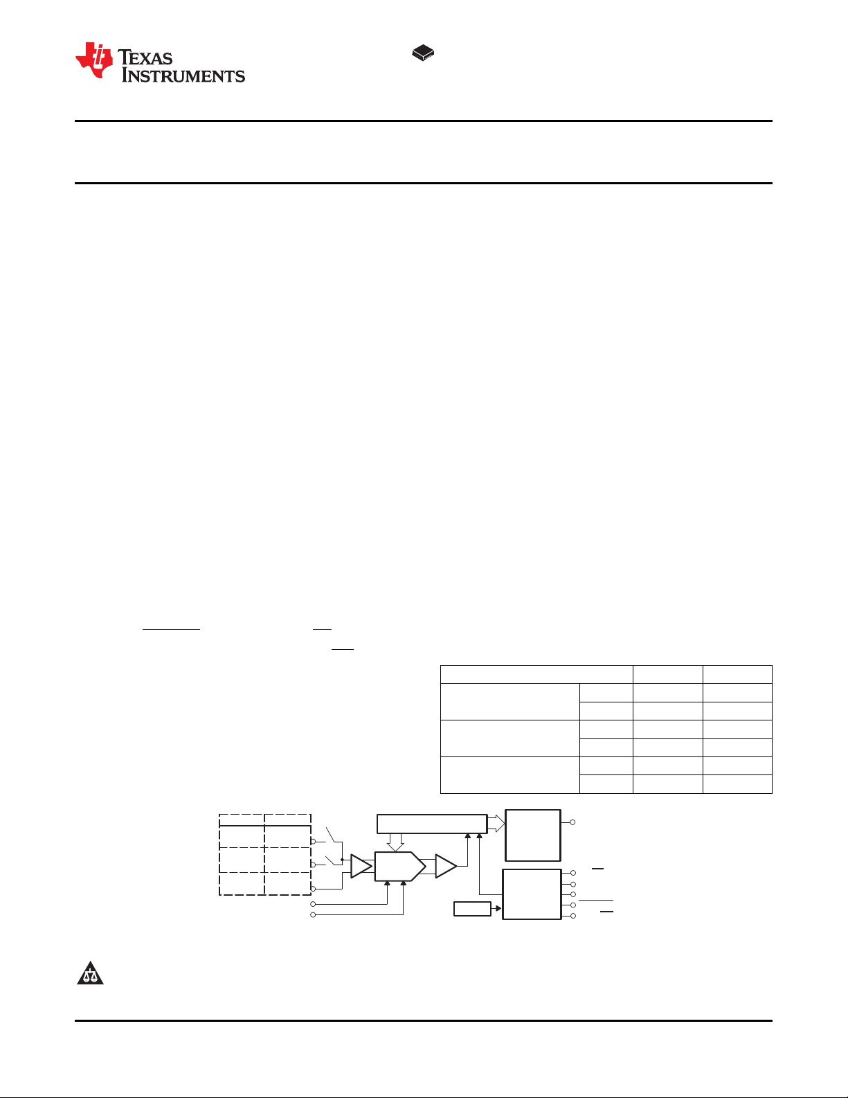
REF
+IN
REF+
SDI
SCLK
SDO
CDAC
SAR
COMPARATOR
OUTPUT
LATCH
and
TRI-STATE
DRIVER
CONVERSION
and
CONTROL
LOGIC
-IN
+IN1
+IN0
COM
NC
OSC
_
+
ADS7230 ADS7229
FS/CS
CONVST
EOC/INT/CDI
ADS7229
ADS7230
www.ti.com
............................................................................................................................................................... SBAS437A – MAY 2008 – REVISED JUNE 2009
LOW-POWER, 12-BIT, 1MHz, SINGLE/DUAL UNIPOLAR INPUT,
ANALOG-TO-DIGITAL CONVERTERS WITH SERIAL INTERFACE
1
FEATURES APPLICATIONS
23
• 2.7V to 5.5V Analog Supply, Low Power:
– 13.7mW (1MHz, +VA = 3V, +VBD = 1.8V)
• 1MHz Sampling Rate 3V ≤ +VA ≤ 5.5V,
900kHz Sampling Rate 2.7V ≤ +VA ≤ 3V
• Excellent DC Performance:
– ± 0.15LSB Typ, ± 0.5LSB Max INL
– ± 0.12LSB Typ, ± 0.5LSB Max DNL
– ± 0.8mV Max Offset Error at 3V
– ± 1.25mV Max Offset Error at 5V
• Excellent AC Performance at fI= 10kHz with
73.9dB SNR, 93.4dB SFDR, – 88.5dB THD
• Built-In Conversion Clock (CCLK)
• 1.65V to 5.5V I/O Supply:
– SPI™/DSP-Compatible Serial Interface
– SCLK up to 50MHz
• Comprehensive Power-Down Modes:
– Deep Power-Down
– Nap Power-Down
– Auto Nap Power-Down
• Unipolar Input Range: 0V to V
• Software Reset
• Global CONVST (Independent of CS)
• Programmable Status/Polarity EOC/ INT
• 4 × 4 QFN-16 and TSSOP-16 Packages
• Multi-Chip Daisy-Chain Mode
• Programmable TAG Bit Output
• Auto/Manual Channel Select Mode (ADS7230)
REF
• Communications
• Transducer Interface
• Medical Instruments
• Magnetometers
• Industrial Process Control
• Data Acquisition Systems
• Automatic Test Equipment
DESCRIPTION
The ADS7229 is a low-power, 12-bit, 1MSPS
analog-to-digital converter (ADC) with a unipolar
input. The device includes a 12-bit capacitor-based
successive approximation register (SAR) ADC with
inherent sample-and-hold.
The ADS7230 is based on the same core and
includes a 2-to-1 input MUX with a programmable
TAG bit output option. Both the ADS7229 and
ADS7230 offer a high-speed, wide voltage serial
interface and are capable of daisy-chain mode
operation when multiple converters are used.
These devices are available in 4 × 4 QFN and
TSSOP-16 packages, and are fully specified for
operation over the industrial – 40 ° C to +85 ° C
temperature range.
Low Power, High-Speed SAR Converter Family
Type/Speed 500 kSPS 1 MSPS
16-bit single-ended
14-bit single-ended
12-bit single-ended
Single ADS8327 ADS8329
Dual ADS8328 ADS8330
Single — ADS7279
Dual — ADS7280
Single — ADS7229
Dual — ADS7230
1
2 SPI is a trademark of Motorola, Inc.
3 All other trademarks are the property of their respective owners.
PRODUCTION DATA information is current as of publication date.
Products conform to specifications per the terms of the Texas
Instruments standard warranty. Production processing does not
necessarily include testing of all parameters.
Please be aware that an important notice concerning availability, standard warranty, and use in critical applications of Texas Instruments semiconductor products and disclaimers thereto appears at the end of this data sheet.
Copyright © 2008 – 2009, Texas Instruments Incorporated
ADS7229
ADS7230
SBAS437A – MAY 2008 – REVISED JUNE 2009 ...............................................................................................................................................................
www.ti.com
This integrated circuit can be damaged by ESD. Texas Instruments recommends that all integrated circuits be handled with
appropriate precautions. Failure to observe proper handling and installation procedures can cause damage.
ESD damage can range from subtle performance degradation to complete device failure. Precision integrated circuits may be more
susceptible to damage because very small parametric changes could cause the device not to meet its published specifications.
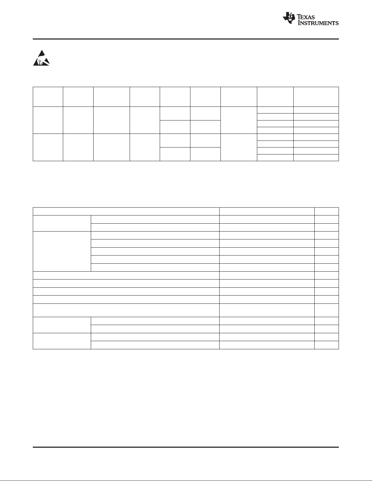
ORDERING INFORMATION
MAXIMUM MAXIMUM MAXIMUM
INTEGRAL DIFFERENTIAL OFFSET TRANSPORT
MODEL (LSB) (LSB) (mV) TYPE DESIGNATOR RANGE INFORMATION QUANTITY
ADS7229I ± 0.5 ± 0.5 ± 1.25 – 40 ° C to +85 ° C
ADS7230I ± 0.5 ± 0.5 ± 1.25 – 40 ° C to +85 ° C
LINEARITY LINEARITY ERROR PACKAGE PACKAGE TEMPERATURE ORDERING MEDIA,
4 × 4 QFN-16 RSA
TSSOP-16 PW
4 × 4 QFN-16 RSA
TSSOP-16 PW
(1)
ADS7229IRSAT Small tape and reel, 250
ADS7229IRSAR Tape and reel, 3000
ADS7229IPW Tube, 90
ADS7229IPWR Tape and reel, 2000
ADS7230IRSAT Small tape and reel, 250
ADS7230IRSAR Tape and reel, 3000
ADS7230IPW Tube, 90
ADS7230IPWR Tape and reel, 2000
(1) For the most current package and ordering information see the Package Option Addendum at the end of this document, or see the TI
web site at www.ti.com .
ABSOLUTE MAXIMUM RATINGS
(1)
Over operating free-air temperature range, unless otherwise noted.
ADS7229, ADS7230 UNIT
Voltage
Voltage range – REF to AGND – 0.3 to 0.3 V
Digital input voltage to BDGND – 0.3 to +VBD + 0.3 V
Digital output voltage to BDGND – 0.3 to +VBD + 0.3 V
T
Operating free-air temperature range – 40 to +85 ° C
A
T
Storage temperature range – 65 to +150 ° C
STG
T
J
Junction temperature +150 ° C
max
4 × 4 QFN-16
package
TSSOP-16
package
(1) Stresses beyond those listed under absolute maximum ratings may cause permanent damage to the device. These are stress ratings
only, and functional operation of the device at these or any other conditions beyond those indicated under recommended operating
conditions is not implied. Exposure to absolute-maximum-rated conditions for extended periods may affect device reliability.
+IN to AGND – 0.3 to +VA + 0.3 V
– IN to AGND – 0.3 to +VA + 0.3 V
+VA to AGND – 0.3 to 7 V
+REF to AGND – 0.3 to +VA + 0.3 V
+VBD to BDGND – 0.3 to 7 V
AGND to BDGND – 0.3 to 0.3 V
Power dissipation (TJmax – TA)/ θ
JA
θJAthermal impedance 47 ° C/W
Power dissipation (TJmax – TA)/ θ
JA
θJAthermal impedance 86 ° C/W
2 Submit Documentation Feedback Copyright © 2008 – 2009, Texas Instruments Incorporated
Product Folder Link(s): ADS7229 ADS7230
ADS7229
ADS7230
www.ti.com
............................................................................................................................................................... SBAS437A – MAY 2008 – REVISED JUNE 2009
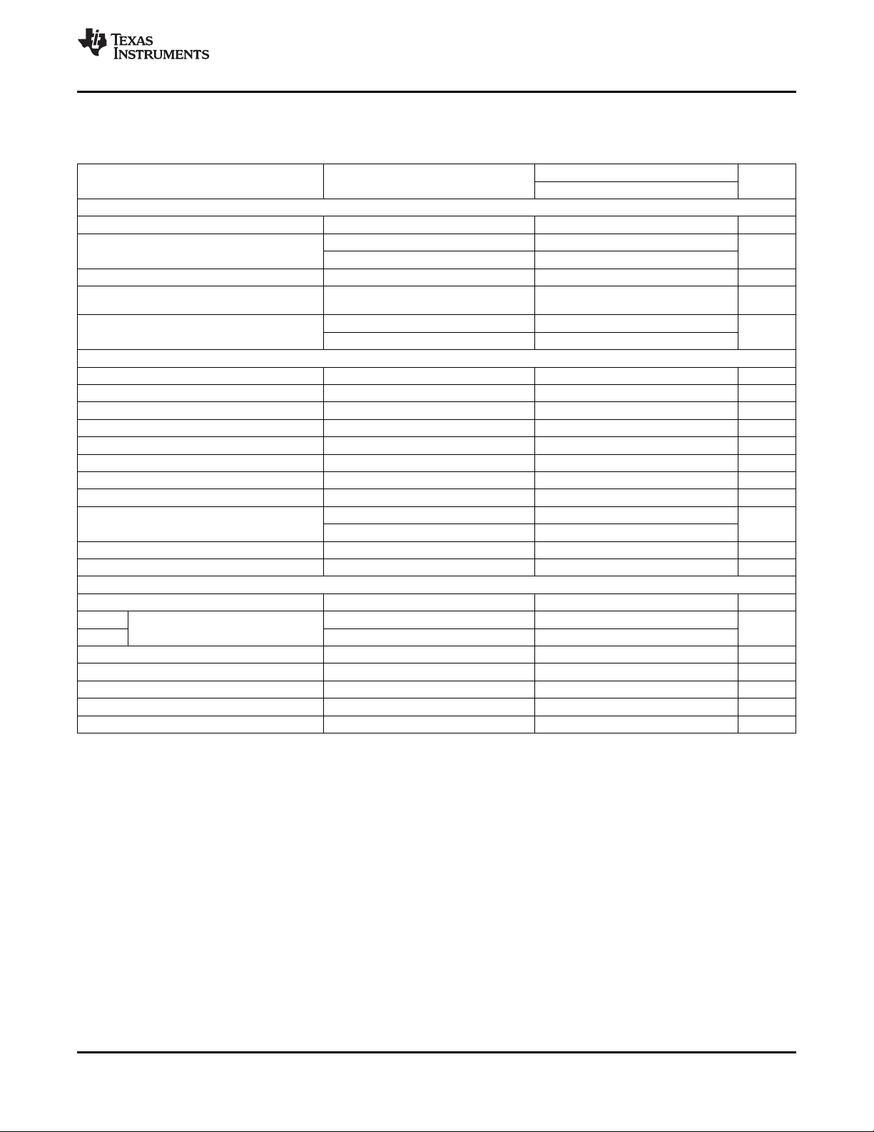
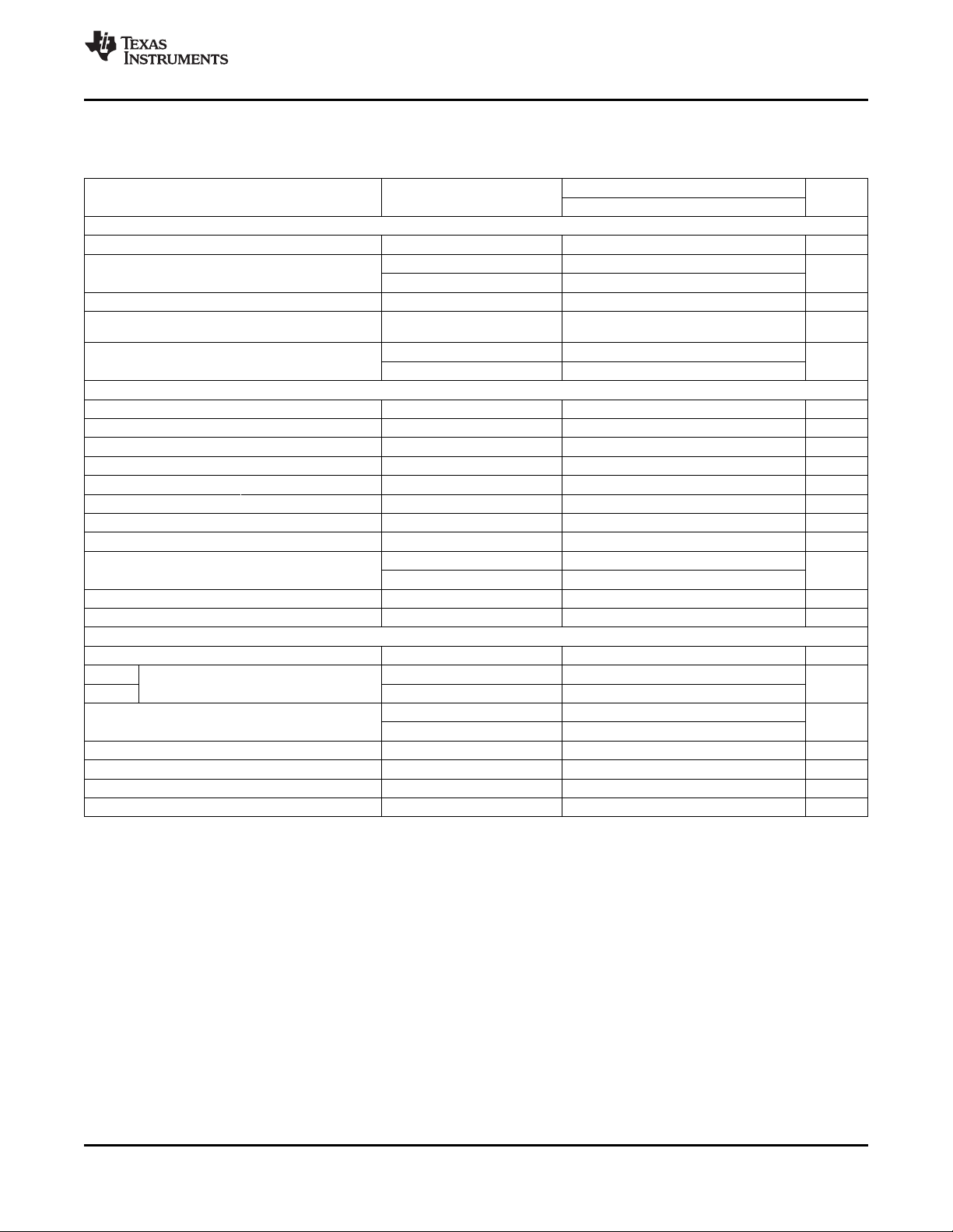
ELECTRICAL CHARACTERISTICS
At TA= – 40 ° C to +85 ° C, +VA = 4.5V to 5.5V, +VBD = +1.65V to +5.5V, V
noted.
PARAMETER TEST CONDITIONS MIN TYP MAX UNIT
ANALOG INPUT
FSR Full-scale input voltage
Absolute input voltage V
Input capacitance 45 pF
Input leakage current 50 nA
Input channel isolation, ADS7230 only dB
SYSTEM PERFORMANCE
Resolution 12 Bits
NMC No missing codes 12 Bits
INL Integral linearity – 0.5 ± 0.15 0.5 LSB
DNL Differential linearity – 0.5 ± 0.12 0.5 LSB
E
O
E
G
CMRR Common-mode rejection ratio dB
PSRR Power-supply rejection ratio At FFFFh output code
SAMPLING DYNAMICS
t
CONV
t
SAMPLE1
t
SAMPLE2
Offset error
Offset error drift FSR = 5V ± 0.2 ppm/ ° C
Gain error – 0.1 ± 0.002 0.1 %FSR
Gain error drift ± 0.5 ppm/ ° C
Noise 33 µ V
Conversion time 18 CCLK
Acquisition time CCLK
Throughput rate 1 MHz
Aperture delay 5 ns
Aperture jitter 10 ps
Step response 100 ns
Overvoltage recovery 100 ns
(3)
(1) Ideal input span; does not include gain or offset error.
(2) LSB means least significant bit.
(3) Measured relative to an ideal full-scale input [(+IN) – ( – IN)] of 4.096V when +VA = 5V.
(1)
+IN – ( – IN) or (+INx – COM) 0 V
+IN, +IN0, +IN1 AGND – 0.2 +VA + 0.2
– IN or COM AGND – 0.2 AGND + 0.2
No ongoing conversion,
dc input
At dc 109
VI= ± 1.25V
At dc 70
VI= 0.4V
Manual trigger 3
Auto trigger 3
at 50kHz 101
PP
at 1MHz 50
PP
(3)
= 5V, and f
REF
= 1MHz, unless otherwise
SAMPLE
ADS7229, ADS7230
REF
– 1.25 ± 0.3 1.25 mV
78 dB
V
(2)
(2)
RMS
Copyright © 2008 – 2009, Texas Instruments Incorporated Submit Documentation Feedback 3
Product Folder Link(s): ADS7229 ADS7230
ADS7229
ADS7230
SBAS437A – MAY 2008 – REVISED JUNE 2009 ...............................................................................................................................................................
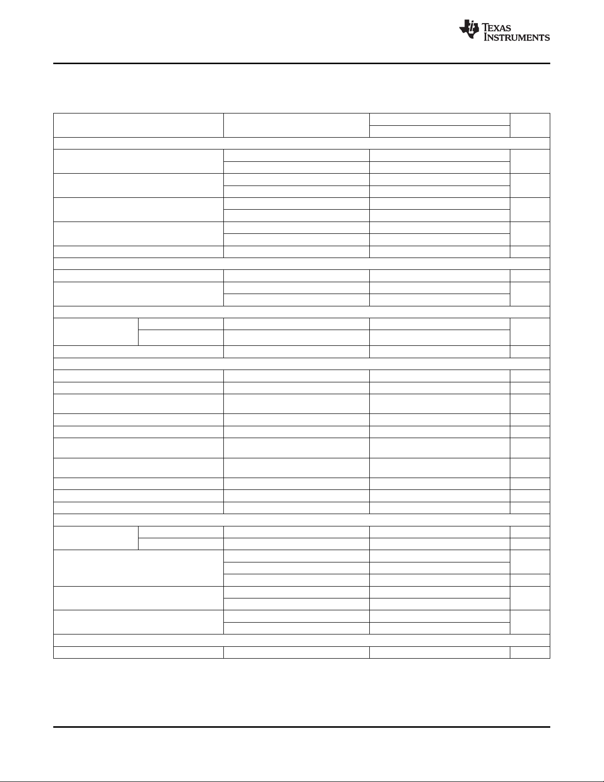
ELECTRICAL CHARACTERISTICS (continued)
At TA= – 40 ° C to +85 ° C, +VA = 4.5V to 5.5V, +VBD = +1.65V to +5.5V, V
noted.
PARAMETER TEST CONDITIONS MIN TYP MAX UNIT
DYNAMIC CHARACTERISTICS
THD Total harmonic distortion
(4)
SNR Signal-to-noise ratio dB
SINAD Signal-to-noise + distortion dB
SFDR Spurious-free dynamic range dB
VIN= 5V
VIN= 5V
VIN= 5V
VIN= 5V
VIN= 5V
VIN= 5V
VIN= 5V
VIN= 5V
– 3dB small-signal bandwidth 30 MHz
CLOCK
Internal conversion clock frequency 21 23 24.5 MHz
SCLK external serial clock MHz
Used as I/O clock only 50
As I/O clock and conversion clock 1 42
EXTERNAL VOLTAGE REFERENCE INPUT
V
REF
reference V
range
Resistance
(5)
Input V
[(REF+) – (REF – )] 0.3 +VA
REF
(REF – ) – AGND – 0.1 0.1
Reference input 40 k Ω
DIGITAL INPUT/OUTPUT
Logic family — CMOS
V
IH
V
IL
I
I
C
I
V
OH
V
OL
C
O
C
L
High-level input voltage 5.5V ≥ +VBD ≥ 4.5V 0.65 × (+VBD) +VBD + 0.3 V
Low-level input voltage 5.5V ≥ +VBD ≥ 4.5V – 0.3 V
Input current VI= +VBD or BDGND – 50 50 nA
Input capacitance 5 pF
High-level output voltage +VBD – 0.6 +VBD V
Low-level output voltage 0 0.4 V
5.5V ≥ +VBD ≥ 4.5V,
IO= 100 µ A
5.5V ≥ +VBD ≥ 4.5V,
IO= 100 µ A
Output capacitance 5 pF
Load capacitance 30 pF
Data format — straight binary
POWER-SUPPLY REQUIREMENTS
Power-supply
voltage
+VBD 1.65 3.3 5.5 V
+VA 4.5 5 5.5 V
1MHz sample rate 5.7 7.0
Supply current Nap or Auto Nap mode 0.3 0.5
Deep power-down mode 4 1 µ A
Buffer I/O supply current mA
Power dissipation mW
1MSPS, BVDD = 1.8V 0.1 0.5
1MSPS, BVDD = 3V 0.5 1.2
AVDD = 5V, BVDD = 1.8V 28.8 36.5
AVDD = 5V, BVDD = 3V 30.0 38.6
TEMPERATURE RANGE
T
A
Operating free-air temperature – 40 +85 ° C
(4) Calculated on the first nine harmonics of the input frequency.
(5) Can vary ± 30%.
at 10kHz – 88.5
PP
at 100kHz – 85.5
PP
at 10kHz 73.9
PP
at 100kHz 72 73.8
PP
at 10kHz 73.7
PP
at 100kHz 73.3
PP
at 10kHz 93.4
PP
at 100kHz 90.5
PP
= 5V, and f
REF
= 1MHz, unless otherwise
SAMPLE
ADS7229, ADS7230
0.35 ×
(+VBD)
www.ti.com
dB
mA
4 Submit Documentation Feedback Copyright © 2008 – 2009, Texas Instruments Incorporated
Product Folder Link(s): ADS7229 ADS7230
ADS7229
ADS7230
www.ti.com
............................................................................................................................................................... SBAS437A – MAY 2008 – REVISED JUNE 2009
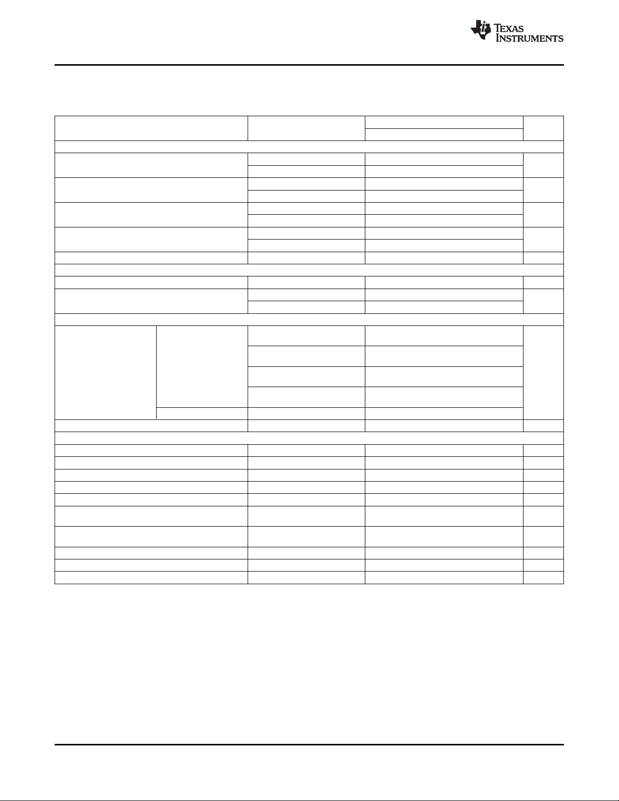
ELECTRICAL CHARACTERISTICS
At TA= – 40 ° C to +85 ° C, +VA = 2.7V to 3.6V, +VBD = 1.65V to 1.5 × (+VA), V
3.6V, and f
ANALOG INPUT
FSR Full-scale input voltage
Absolute input voltage V
Input capacitance 45 pF
Input leakage current 50 nA
Input channel isolation, ADS7230 only dB
SYSTEM PERFORMANCE
Resolution 12 Bits
No missing codes 12 Bits
INL Integral linearity – 0.5 ± 0.15 0.5 LSB
DNL Differential linearity – 0.5 ± 0.12 0.5 LSB
E
O
E
G
CMRR Common-mode rejection ratio dB
PSRR Power-supply rejection ratio At FFFFh output code
SAMPLING DYNAMICS
t
CONV
t
SAMPLE1
t
SAMPLE2
(1) Ideal input span; does not include gain or offset error.
(2) LSB means least significant bit.
(3) Measured relative to an ideal full-scale input [(+IN) – ( – IN)] of 2.5V when +VA = 3V.
Offset error
Offset error drift FSR = 2.5V ± 0.1 ppm/ ° C
Gain error – 0.1 ± 0.008 0.1 %FSR
Gain error drift ± 0.3 ppm/ ° C
Noise 33 µ V
Conversion time 18 CCLK
Acquisition time CCLK
Throughput rate MHz
Aperture delay 5 ns
Aperture jitter 10 ps
Step response 100 ns
Overvoltage recovery 100 ns
= 900kHz for 3V < +VA ≤ 2.7V using external clock, unless otherwise noted.
SAMPLE
PARAMETER TEST CONDITIONS MIN TYP MAX UNIT
(1)
(3)
+IN – ( – IN) or (+INx – COM) 0 V
+IN, +IN0, +IN1 AGND – 0.2 +VA + 0.2
– IN or COM AGND – 0.2 AGND + 0.2
No ongoing conversion,
dc Input
At dc 108
VI= ± 1.25V
At dc 70
VI= 0.4V
Manual trigger 3
Auto trigger 3
2.7V ≤ +VA < 3.0V 0.9
3.0V ≤ +VA ≤ 3.64V 1
at 50kHz 101
PP
at 1MHz 50
PP
(3)
REF
= 2.5V, f
ADS7229, ADS7230
– 0.8 ± 0.07 0.8 mV
= 1MHz for 3V ≤ +VA ≤
SAMPLE
78 dB
REF
V
(2)
(2)
RMS
Copyright © 2008 – 2009, Texas Instruments Incorporated Submit Documentation Feedback 5
Product Folder Link(s): ADS7229 ADS7230
ADS7229
ADS7230
SBAS437A – MAY 2008 – REVISED JUNE 2009 ...............................................................................................................................................................
ELECTRICAL CHARACTERISTICS (continued)
At TA= – 40 ° C to +85 ° C, +VA = 2.7V to 3.6V, +VBD = 1.65V to 1.5 × (+VA), V
3.6V, and f
DYNAMIC CHARACTERISTICS
THD Total harmonic distortion
SNR Signal-to-noise ratio dB
SINAD Signal-to-noise + distortion dB
SFDR Spurious-free dynamic range dB
– 3dB small-signal bandwidth 30 MHz
CLOCK
Internal conversion clock frequency 21 23 23.5 MHz
SCLK external serial clock MHz
EXTERNAL VOLTAGE REFERENCE INPUT
V
REF
DIGITAL INPUT/OUTPUT
V
IH
V
IL
I
I
C
I
V
OH
V
OL
C
O
C
L
(4) Calculated on the first nine harmonics of the input frequency.
(5) Can vary ± 30%.
Input reference
range 2.475 2.525
Resistance
Logic family — CMOS
High-level input voltage (+VA × 1.5)V ≥ +VBD ≥ 1.65V 0.65 × (+VBD) +VBD + 0.3 V
Low-level input voltage (+VA × 1.5)V ≥ +VBD ≥ 1.65V – 0.3 0.35 × (+VBD) V
Input current VI= +VBD or BDGND – 50 50 nA
Input capacitance 5 pF
High-level output voltage +VBD – 0.6 +VBD V
Low-level output voltage 0 0.4 V
Output capacitance 5 pF
Load capacitance 30 pF
Data format — straight binary
= 900kHz for 3V < +VA ≤ 2.7V using external clock, unless otherwise noted.
SAMPLE
PARAMETER TEST CONDITIONS MIN TYP MAX UNIT
(4)
VIN= 2.5V
VIN= 2.5V
VIN= 2.5V
VIN= 2.5V
VIN= 2.5V
VIN= 2.5V
VIN= 2.5V
VIN= 2.5V
at 10kHz – 96.8
PP
at 100kHz – 88.4
PP
at 10kHz 72 73.2
PP
at 100kHz 72
PP
at 10kHz 73.1
PP
at 100kHz 72.1
PP
at 10kHz 95.9
PP
at 100kHz 91.5
PP
Used as I/O clock only 42
As I/O clock and conversion clock 1 42
f
≤ 500kSPS,
SAMPLE
2.7V ≤ +VA < 3V
f
≤ 500kSPS,
SAMPLE
V
[(REF+) – (REF – )]
REF
3V ≤ +VA < 3.6V
f
> 500kSPS, V
SAMPLE
2.7V ≤ +VA < 3V
f
> 500kSPS,
SAMPLE
3V ≤ +VA ≤ 3.6V
(REF – ) – AGND – 0.1 0.1
(5)
Reference input 40 k Ω
(+VA × 1.5)V ≥ +VBD ≥ 1.65V,
IO= 100 µ A
(+VA × 1.5)V ≥ +VBD ≥ 1.65V,
IO= 100 µ A
REF
= 2.5V, f
= 1MHz for 3V ≤ +VA ≤
SAMPLE
ADS7229, ADS7230
0.3 2.525
0.3 3
2.475 3
www.ti.com
dB
6 Submit Documentation Feedback Copyright © 2008 – 2009, Texas Instruments Incorporated
Product Folder Link(s): ADS7229 ADS7230
ADS7229
ADS7230
www.ti.com
............................................................................................................................................................... SBAS437A – MAY 2008 – REVISED JUNE 2009
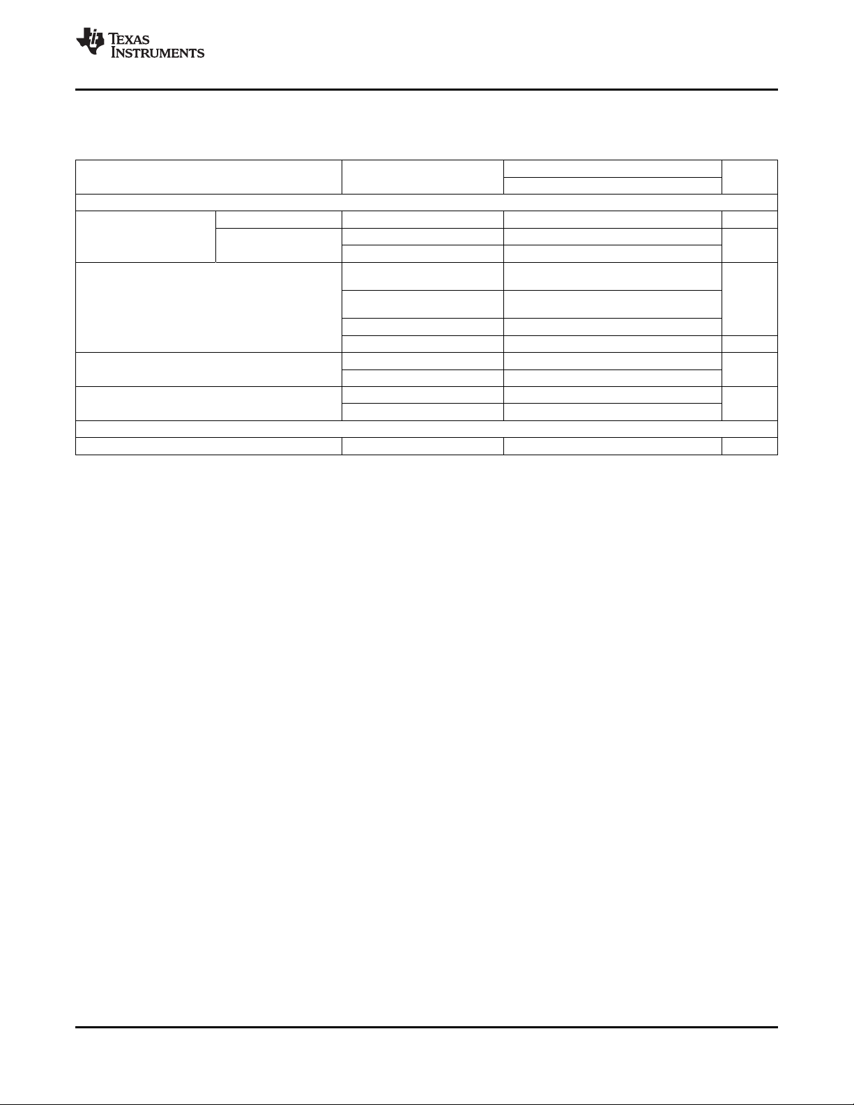
ELECTRICAL CHARACTERISTICS (continued)
At TA= – 40 ° C to +85 ° C, +VA = 2.7V to 3.6V, +VBD = 1.65V to 1.5 × (+VA), V
3.6V, and f
POWER-SUPPLY REQUIREMENTS
TEMPERATURE RANGE
T
A
Power-supply
voltage
Supply current
Buffer I/O supply current mA
Power dissipation mW
Operating free-air temperature – 40 +85 ° C
= 900kHz for 3V < +VA ≤ 2.7V using external clock, unless otherwise noted.
SAMPLE
PARAMETER TEST CONDITIONS MIN TYP MAX UNIT
+VBD 1.65 +VA 1.5 × (+VA) V
+VA V
fs≤ 1MHz 3 3.6
fs≤ 900kHz 2.7 3.6
1MHz sample rate,
3V ≤ +VA ≤ 3.6V
900kHz sample rate, mA
2.7V ≤ +VA ≤ 3V
Nap or Auto Nap mode 0.25 0.4
Deep power-down mode 0.001 1 µ A
1MSPS, BVDD = 1.8V 0.1 0.5
1MSPS, BVDD = 3V 0.5 1.2
AVDD = 3V, BVDD = 1.8V 13.7 18.9
AVDD = 3V, BVDD = 3V 15.0 21.6
REF
= 2.5V, f
= 1MHz for 3V ≤ +VA ≤
SAMPLE
ADS7229, ADS7230
4.5 6.0
4.2
Copyright © 2008 – 2009, Texas Instruments Incorporated Submit Documentation Feedback 7
Product Folder Link(s): ADS7229 ADS7230
ADS7229
ADS7230
SBAS437A – MAY 2008 – REVISED JUNE 2009 ...............................................................................................................................................................
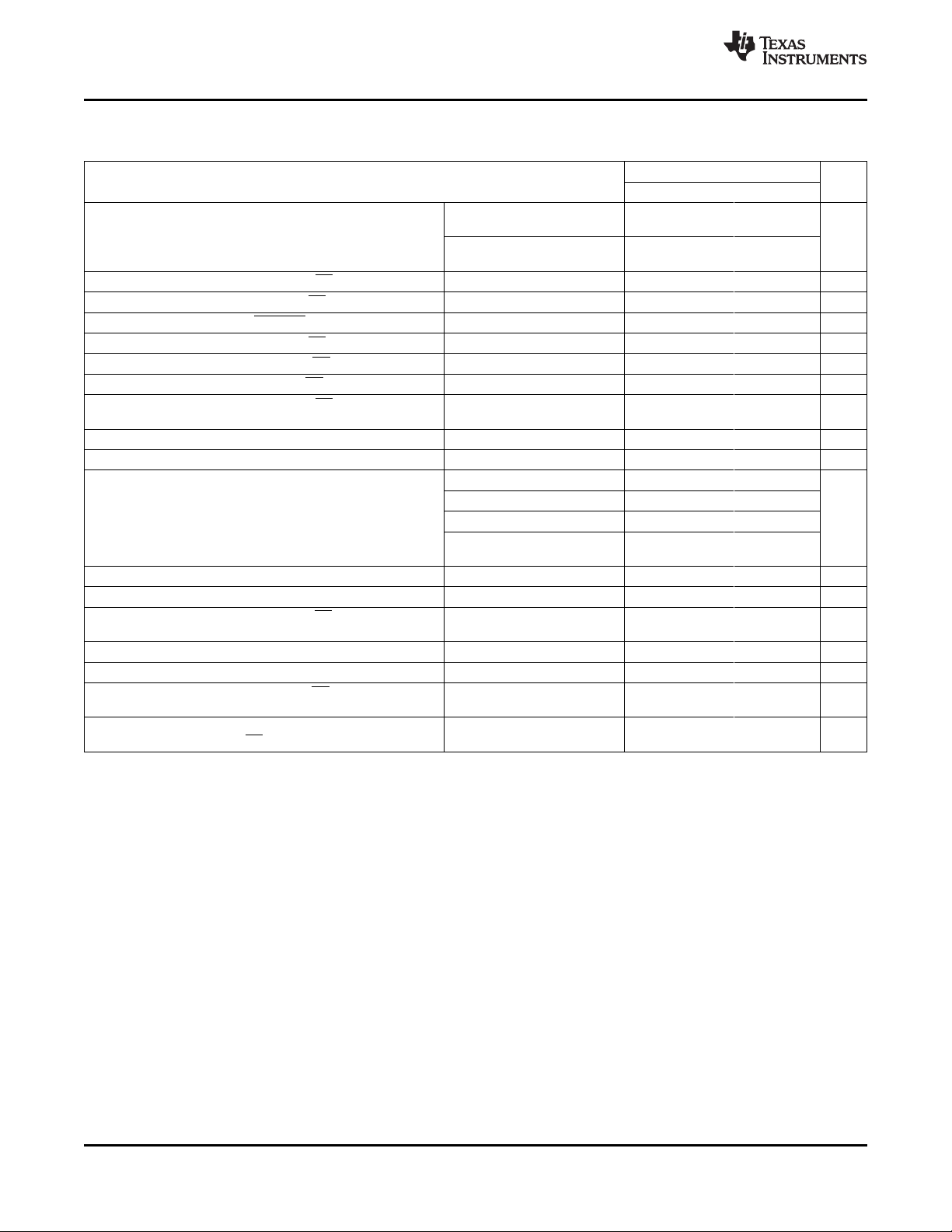
TIMING CHARACTERISTICS
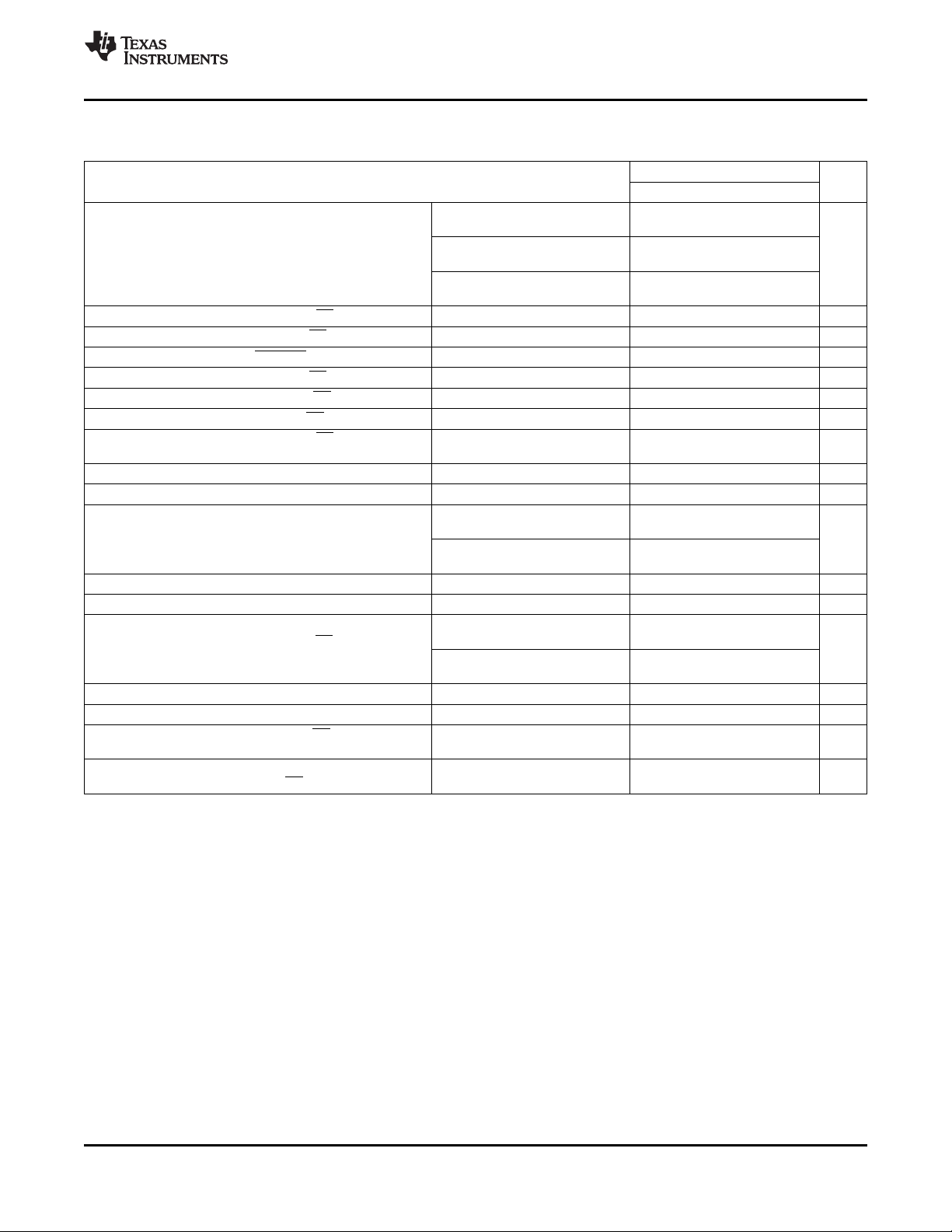
(1) (2)
: 5V
All specifications typical at – 40 ° C to +85 ° C and +VA = +VBD = 5V, unless otherwise noted.
PARAMETER MIN TYP MAX UNIT
External,
f
= 1/2 f
f
CCLK
t
1
t
2
t
CL
t
3
t
4
t
5
t
6
t
SCLKL
t
SCLKH
Frequency, conversion clock, CCLK MHz
Setup time, falling edge of CS to EOC 1 CCLK
Hold time, falling edge of CS to EOC 0 ns
Pulse duration, CONVST low 40 ns
Hold time, falling edge of CS to EOS 20 ns
Setup time, rising edge of CS to EOS 20 ns
Hold time, rising edge of CS to EOS 20 ns
Setup time, falling edge of CS to first falling
SCLK
Pulse duration, SCLK low 8 t
Pulse duration, SCLK high 8 t
CCLK
Internal,
f
CCLK
= 1/2 f
SCLK
SCLK
I/O clock only 20
I/O and conversion clock 23.8 2000
t
SCLK
Cycle time, SCLK ns
I/O clock, chain mode 20
I/O and conversion clock,
chain mode
t
H2
t
D1
t
D2
t
S1
t
H1
t
D3
t
7
Hold time, falling edge of SCLK to SDO invalid 10pF load 2 ns
Delay time, falling edge of SCLK to SDO valid 10pF load 10 ns
Delay time, falling edge of CS to SDO valid,
SDO MSB output
10pF load 8.5 ns
Setup time, SDI to falling edge of SCLK 8 ns
Hold time, SDI to falling edge of SCLK 4 ns
Delay time, rising edge of CS/FS to SDO t
3-state
D3
Setup time, 16th falling edge of SCLK before
rising edge of CS/FS
(1) All input signals are specified with tr= tf= 1.5ns (10% to 90% of VBD) and timed from a voltage level of (V
(2) See timing diagrams.
0.5 21
21 23 24.5
23.8 2000
10 ns
www.ti.com
ADS7229, ADS7230
5 ns
– 8 ns
SCLK
– 8 ns
SCLK
+ VIH)/2.
IL
5 ns
8 Submit Documentation Feedback Copyright © 2008 – 2009, Texas Instruments Incorporated
Product Folder Link(s): ADS7229 ADS7230
ADS7229
ADS7230
www.ti.com
TIMING CHARACTERISTICS
............................................................................................................................................................... SBAS437A – MAY 2008 – REVISED JUNE 2009
(1) (2)
: 1.8V
All specifications typical at – 40 ° C to 85 ° C, +VA = 2.7 V, and +VBD = 1.8V, unless otherwise noted.
PARAMETER MIN TYP MAX UNIT
External, 3V ≤ +VA ≤ 3.6V,
f
= 1/2 f
CCLK
f
CCLK
Frequency, conversion clock, CCLK 0.5 18.9 MHz
External, 2.7V ≤ +VA ≤ 3V,
f
CCLK
Internal,
f
CCLK
t
1
t
2
t
CL
t
3
t
4
t
5
t
6
t
SCLKL
t
SCLKH
Setup time, falling edge of CS to EOC 1 CCLK
Hold time, falling edge of CS to EOC 0 ns
Pulse duration, CONVST low 40 ns
Hold time, falling edge of CS to EOS 20 ns
Setup time, rising edge of CS to EOS 20 ns
Hold time, rising edge of CS to EOS 20 ns
Setup time, falling edge of CS to first t6falling
SCLK
Pulse duration, SCLK low 8 t
Pulse duration, SCLK high 8 t
All modes,
t
SCLK
Cycle time, SCLK ns
3V ≤ +VA ≤ 3.6V
All modes,
2.7V ≤ +VA < 3V
t
H2
t
D1
Hold time, falling edge of SCLK to SDO invalid 10pF load 7.5 ns
Delay time, falling edge of SCLK to SDO valid 10pF load 16 ns
10pF load,
t
D2
Delay time, falling edge of CS to SDO valid,
SDO MSB output
2.7V ≤ +VA ≤ 3V
10pF load,
3V ≤ +VA ≤ 3.6V
t
S1
t
H1
t
D3
t
7
Setup time, SDI to falling edge of SCLK 8 ns
Hold time, SDI to falling edge of SCLK 4 ns
Delay time, rising edge of CS/FS to SDO
3-state
Setup time, 16th falling edge of SCLK t
before rising edge of CS/FS
7
(1) All input signals are specified with tr= tf= 1.5ns (10% to 90% of VBD) and timed from a voltage level of (V
(2) See timing diagrams.
= 1/2 f
= 1/2 f
SCLK
SCLK
SCLK
23.8 2000
26.5 2000
ADS7229, ADS7230
0.5 21
20 22.3 23.5
5 ns
– 8 ns
SCLK
– 8 ns
SCLK
13
11
10 ns
+ VIH)/2.
IL
ns
8 ns
Copyright © 2008 – 2009, Texas Instruments Incorporated Submit Documentation Feedback 9
Product Folder Link(s): ADS7229 ADS7230
REF+(REFIN)
NC
CONVST
EOC/ /CDIINT
RESERVED
+VA
+VBD
SCLK
1
2
3
4
12
11
10
9
REF-
16
FS/
CS
5
AGND
15
SDI
6
-IN
14
SDO
7
+IN
13
BDGND
8
REF+(REFIN)
NC
CONVST
EOC/ /CDIINT
+IN1
+VA
+VBD
SCLK
1
2
3
4
12
11
10
9
REF-
16
FS/CS
5
AGND
15
SDI
6
COM
14
SDO
7
+IN0
13
BDGND
8
+VBD
SCLK
BDGND
SDO
SDI
FS/CS
EOC/INT/CDI
CONVST
+VA
RESERVED
+IN
-IN
AGND
REF-
REF+(REFIN)
NC
1
2
3
4
5
6
7
8
16
15
14
13
12
11
10
9
+VBD
SCLK
BDGND
SDO
SDI
FS/CS
EOC/INT/CDI
CONVST
+VA
+IN1
+IN0
COM
AGND
REF-
REF+(REFIN)
NC
1
2
3
4
5
6
7
8
16
15
14
13
12
11
10
9
ADS7229
ADS7230
SBAS437A – MAY 2008 – REVISED JUNE 2009 ...............................................................................................................................................................
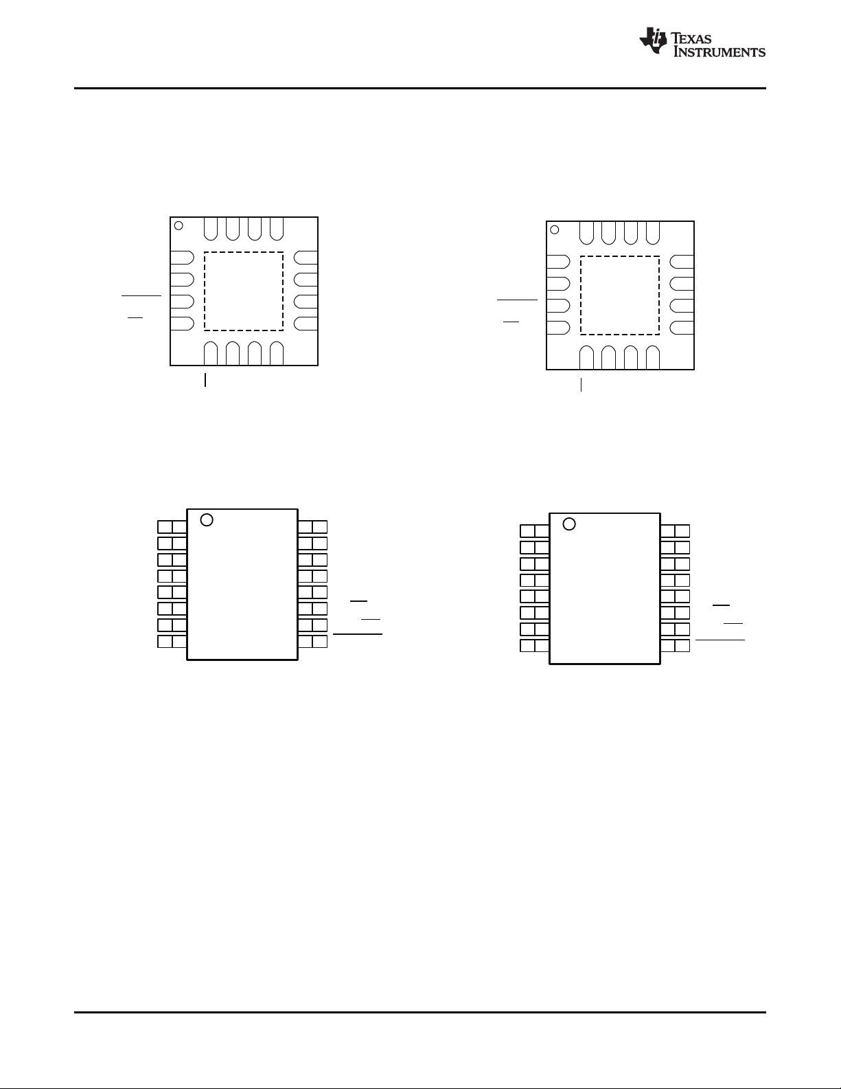
PIN ASSIGNMENTS
ADS7229
RSA PACKAGE (QFN)
(TOP VIEW)
CAUTION: The thermal pad is internally connected to the substrate. This pad can be connected to the analog
ground or left floating. Keep the thermal pad separate from the digital ground, if possible.
ADS7229
PW PACKAGE (TSSOP)
(TOP VIEW)
ADS7230
RSA PACKAGE (QFN)
(TOP VIEW)
ADS7230
PW PACKAGE (TSSOP)
(TOP VIEW)
www.ti.com
NC = No internal connection
Product Folder Link(s): ADS7229 ADS7230
10 Submit Documentation Feedback Copyright © 2008 – 2009, Texas Instruments Incorporated
ADS7229
ADS7230
www.ti.com
............................................................................................................................................................... SBAS437A – MAY 2008 – REVISED JUNE 2009
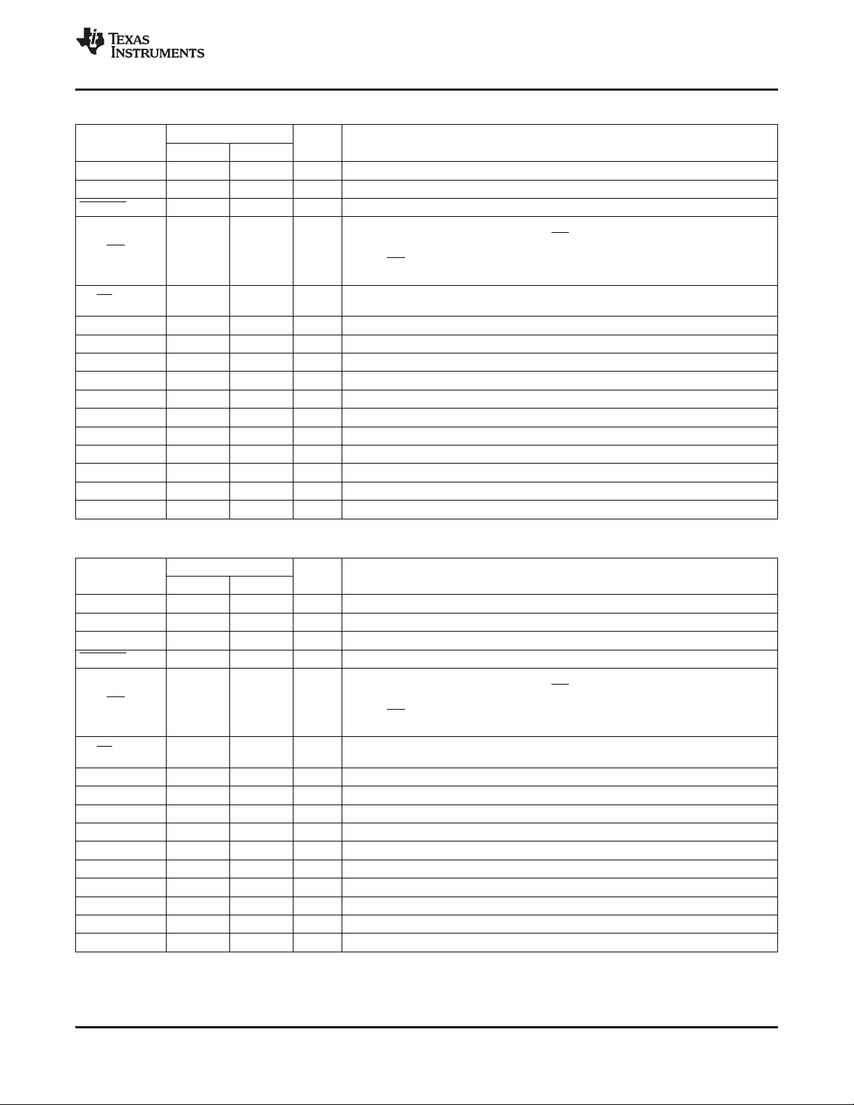
ADS7229 Terminal Functions
NO.
NAME QFN TSSOP I/O DESCRIPTION
AGND 15 5 — Analog ground
BDGND 8 14 — Interface ground
CONVST 3 9 I Freezes sample-and-hold, starts conversion with next rising edge of internal clock
Status output. If programmed as EOC, this pin is low (default) when a conversion is in
EOC/ INT/CDI 4 10 I/O duration after the end of conversion and valid data are to be output. The polarity of
FS/ CS 5 11 I
+IN 13 3 I Noninverting input
– IN 14 4 I Inverting input; usually connected to ground
NC 2 8 — No connection
REF+ (REFIN) 1 7 I External reference input
REF – 16 6 I Connect to AGND through individual via
RESERVED 12 2 I Connect to AGND or +VA
SCLK 9 15 I Clock for serial interface
SDI 6 12 I Serial data in
SDO 7 13 O Serial data out
+VA 11 1 Analog supply, +2.7V to +5.5VDC
+VBD 10 16 Interface supply
progress. If programmed as an interrupt ( INT), this pin is low for a preprogrammed
EOC or INT is programmable. This pin can also be used as a chain data input when
the device is operated in daisy-chain mode.
Frame sync signal for TMS320 DSP serial interface or chip select input for SPI
interface slave select (SS – ).
ADS7230 Terminal Functions
NO.
NAME QFN TSSOP I/O DESCRIPTION
AGND 15 5 — Analog ground
BDGND 8 14 — Interface ground
COM 14 4 I Common inverting input; usually connected to ground
CONVST 3 9 I Freezes sample-and-hold, starts conversion with next rising edge of internal clock
Status output. If programmed as EOC, this pin is low (default) when a conversion is in
EOC/ INT/CDI 4 10 I/O duration after the end of conversion and valid data are to be output. The polarity of
FS/ CS 5 11 I
+IN1 12 2 I Second noninverting input
+IN0 13 3 I First noninverting input
NC 2 8 — No connection.
REF+ (REFIN) 1 7 I External reference input
REF – 16 6 I Connect to AGND through individual via
SCLK 9 15 I Clock for serial interface
SDI 6 12 I Serial data in (conversion start and reset possible)
SDO 7 13 O Serial data out
+VA 11 1 Analog supply, +2.7V to +5.5VDC
+VBD 10 16 Interface supply
progress. If programmed as an interrupt ( INT), this pin is low for a preprogrammed
EOC or INT is programmable. This pin can also be used as a chain data input when
the device is operated in daisy-chain mode.
Frame sync signal for TMS320 DSP serial interface or chip select input for SPI
interface
Copyright © 2008 – 2009, Texas Instruments Incorporated Submit Documentation Feedback 11
Product Folder Link(s): ADS7229 ADS7230
E CO
(activelow)
CONVST
FS/CS
INT
(activelow)
SCLK
MANUAL TRIGGER/READ WhileSampling
(useinternalCCLK,EOC,and polarityprogrammedasactivelow)INT
S OD
S ID
Nth
EO
C
EO
S
EOC
Nth
Nth 1-
1………… ………… 16 1
Nth
1101b
READResult
1101b
READResult
t
4
t
SAMPLE1
=3CCLKsMin
t =
CONV
18CCLKs
t
CL
t
2
NthNth 1-
EOC
(activelow)
CONVST
FS/CS
INT
(activelow)
SCLK
MANUAL IGGE EADTR R/R WhileConverting
(useinternalCCLK,EOC,and polarityprogrammedasactivelow)
INT
SDO
SDI
Nth
EOS
EO
S
EO
C
t
SAMPLE1
=3CCLKsMin
Nth
Nth 1-
1……………………16 1
Nth
1101b
READResult
1101b
READResult
t
4
t
CONV
= 18 CCLKs
t
CL
t
3
N+1st
Nth+1
ADS7229
ADS7230
SBAS437A – MAY 2008 – REVISED JUNE 2009 ...............................................................................................................................................................
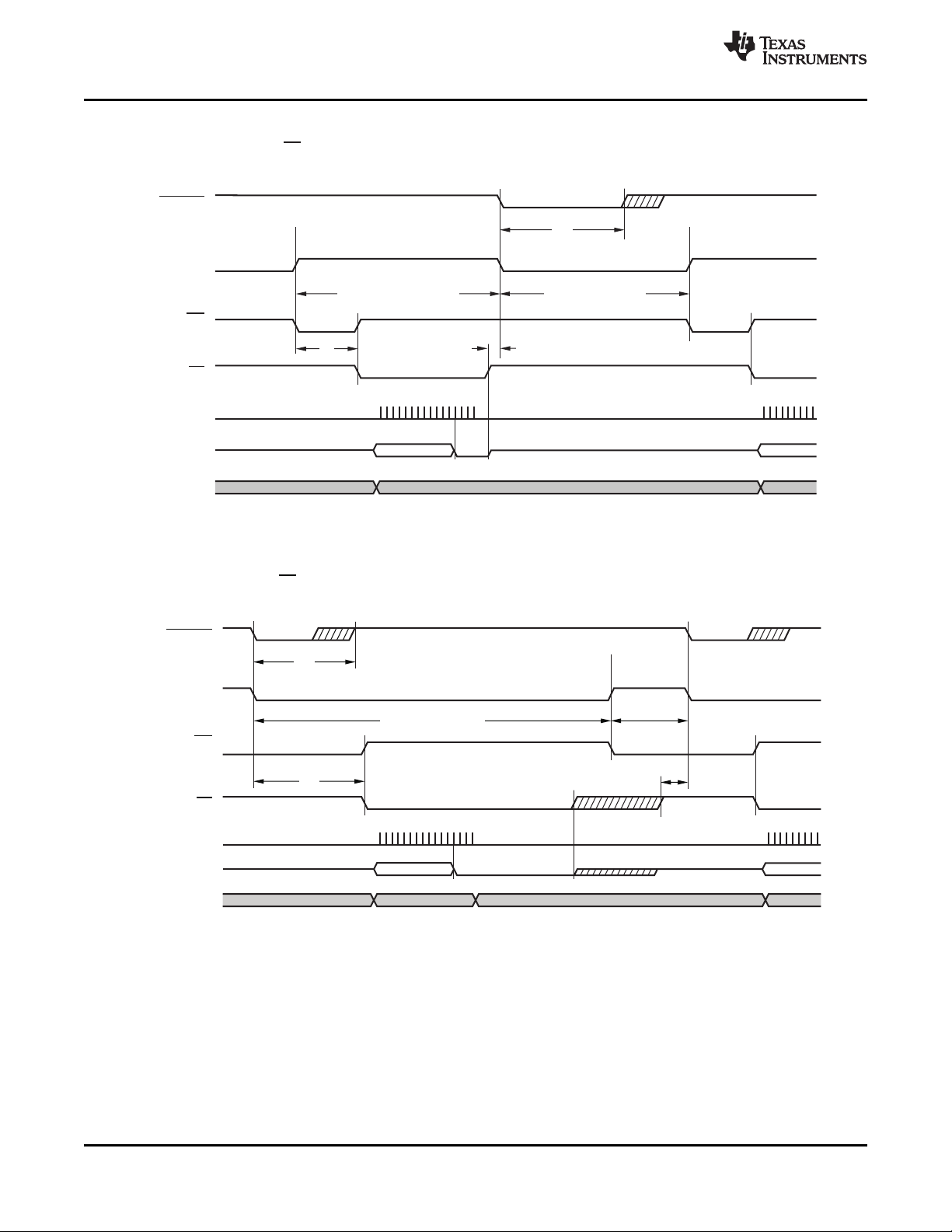
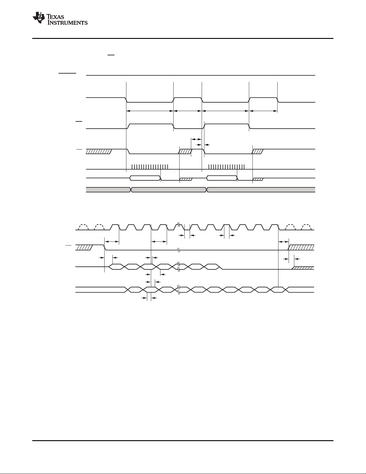
Figure 1. Timing for Conversion and Acquisition Cycles for Manual Trigger (Read While Sampling)
www.ti.com
12 Submit Documentation Feedback Copyright © 2008 – 2009, Texas Instruments Incorporated
Figure 2. Timing for Conversion and Acquisition Cycles for Manual Trigger (Read While Converting)
Product Folder Link(s): ADS7229 ADS7230
EOC
(activelow)
CONVST =1
FS/CS
INT
(activelow)
SCLK
AUTOTRIGGER/READWhileConverting
(useinternalCCLK,EOC,and polarityprogrammedasactivelow)
INT
SDO
SDI
EO
S
Nth
N - 1st
1……………………16
1101b
READResult
1……………………16
N - 2nd
EOC
EO
S
EO
C
t
SAMPLE2
=
3CCLKs
t
SAMPLE2
=
3CCLKs
N - 1th
EOS
1101b
READResult
t
4
t
3
t
CONV
=18CCLKs t
CONV
=18CCLKs
Nth
Nth+1
SCLK
FS/CS
SDO
SDIor DC I
t
H1
t
7
1 2 3 4 11 14 15 16
MSB MSB 1- MSB 2-
MSB 3-
LSB
t
6
t
D2
t
S1
LSB+4 LSB+2
LSB+3
LSB+1 LSBMSB MSB 1- MSB 2-
MSB 3-
t
H2
t
D1
t
D3
t
SCLK
t
SCLKH
t
SCLKL
1312
LSB+1
LSB+5
ADS7229
ADS7230
www.ti.com
............................................................................................................................................................... SBAS437A – MAY 2008 – REVISED JUNE 2009
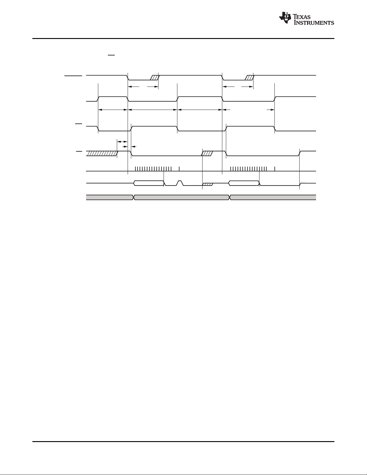
Figure 3. Timing for Conversion and Acquisition Cycles for Autotrigger (Read While Converting)
Copyright © 2008 – 2009, Texas Instruments Incorporated Submit Documentation Feedback 13
Figure 4. Detailed SPI Transfer Timing
Product Folder Link(s): ADS7229 ADS7230
EOC
(activelow)
CONVST
FS/CS
INT
(activelow)
SCLK
M ALANU TRIGGER/READ WhileConvert gin
(useinternalCCLK,EOC,and polarityprogrammedasactivelow,TAGenabled,autochannelselect)
INT
SDO
SDI
NthCH0
EOS
t
SAMPLE1
=
3CCLKsMin
t
SAMPLE1
=
3CCLKsMin
NthCH0
N 1stC- H1
1……………………16
1101b
READResult
1101b
READResult
17
EO
C
EOS
EO
C
NthCH1
NthCH1
EOC
NthCH0
1……………………16 17
TAG=1 TAG=0
High-ZHigh-ZHigh-Z
t
4
t
3
t
CONV
=18CCLKs
t
CONV
=18CCLKs
t
CL
t
CL
ADS7229
ADS7230
SBAS437A – MAY 2008 – REVISED JUNE 2009 ...............................................................................................................................................................
www.ti.com
Figure 5. Simplified Dual Channel Timing
14 Submit Documentation Feedback Copyright © 2008 – 2009, Texas Instruments Incorporated
Product Folder Link(s): ADS7229 ADS7230
Frequency(kHz)
Crosstalk(dB)
20
110
105
100
95
90
85
80
0
40 60 80 100 120 140 160 180
5V
3V
200
T °emperature( C)
DNL(LSB)
-15
0.30
0.25
0.20
0.15
0.10
0.05
0
-40
3V
5V
85
10 35 60
Temperature(°C)
INL(LSB)
-15
0.30
0.25
0.20
0.15
0.10
0.05
0
-40
3V
5V
85
10 35 60
f (MHz)
SCLK
DNL(LSB)
0.50
0.25
0
-0.25
-0.50
0.1 1001 10
+VA=5V
DNL+
DNL-
f (MHz)
SCLK
INL(LSB)
0.50
0.25
0
-0.25
-0.50
0.1 1001 10
+VA=5V
INL+
INL-
f (MHz)
SCLK
DNL(LSB)
0.50
0.25
0
-0.25
-0.50
0.1 1001 10
+VA=3V
DNL+
DNL-
ADS7229
ADS7230
www.ti.com
............................................................................................................................................................... SBAS437A – MAY 2008 – REVISED JUNE 2009
At – 40 ° C to +85 ° C, V
+VBD = 3V, f
for ac curves with 5V supply, and fI= 10kHz for ac curves with 3V supply, unless otherwise noted.
TYPICAL CHARACTERISTICS
[(REF+) – (REF – )] = 5V when +VA = +VBD = 5V or V
REF
= 42MHz, or V
SCLK
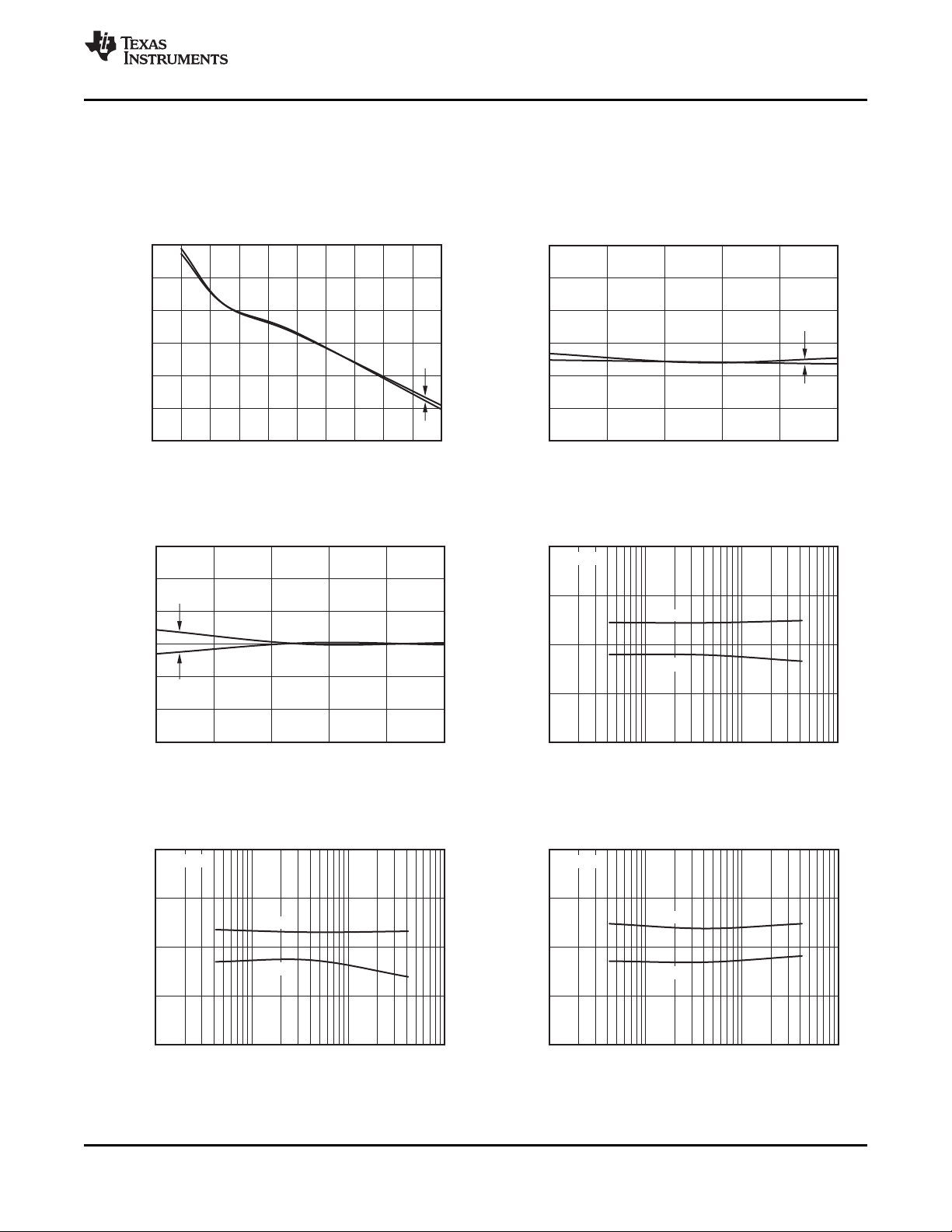
CROSSTALK DIFFERENTIAL NONLINEARITY
vs FREQUENCY vs FREE-AIR TEMPERATURE
INTEGRAL NONLINEARITY DIFFERENTIAL NONLINEARITY
vs FREE-AIR TEMPERATURE vs EXTERNAL CLOCK FREQUENCY
= 2.5 when +VA = +VBD = 2.7V, f
REF
= 37.8MHz, and fI= dc for dc curves, fI= 100kHz
SCLK
Figure 6. Figure 7.
[(REF+) – (REF – )] = 2.5V when +VA =
REF
Copyright © 2008 – 2009, Texas Instruments Incorporated Submit Documentation Feedback 15
Figure 8. Figure 9.
INTEGRAL NONLINEARITY DIFFERENTIAL NONLINEARITY
vs EXTERNAL CLOCK FREQUENCY vs EXTERNAL CLOCK FREQUENCY
Figure 10. Figure 11.
Product Folder Link(s): ADS7229 ADS7230
Temperature( C)°
OffsetVoltage(mV)
-15
0.50
0.25
0
-0.25
-0.50
-40 8510 35 60
5V
3V
f (MHz)
SCLK
INL(LSB)
0.50
0.25
0
-0.25
-0.50
0.1 1001 10
+VA=3V
INL+
INL-
Temperature( C)°
GainError(%FSR)
-15
0.050
0.025
0
-0.025
-0.050
-40
3V
5V
85
10 35 60
+VASupplyVoltage(V)
OffsetVoltage(mV)
0.5
0.4
0.3
0.2
0.1
0
-0.1
2.5 5.53.0
3.5 4.0 4.5 5.0
+VASupplyVoltage(V)
GainError(%FSR)
0.10
0.05
0
-0.05
-0.10
2.5 5.53.0 3.5 4.0 4.5 5.0
Frequency(kHz)
PSRR(dB)
-70
-72
-74
-76
-78
-80
0 10010
20 30 40 50 60 70 80 90
5V
3V
ADS7229
ADS7230
SBAS437A – MAY 2008 – REVISED JUNE 2009 ...............................................................................................................................................................
TYPICAL CHARACTERISTICS (continued)
At – 40 ° C to +85 ° C, V
+VBD = 3V, f
SCLK
for ac curves with 5V supply, and fI= 10kHz for ac curves with 3V supply, unless otherwise noted.
vs EXTERNAL CLOCK FREQUENCY vs FREE-AIR TEMPERATURE
[(REF+) – (REF – )] = 5V when +VA = +VBD = 5V or V
REF
= 42MHz, or V
= 2.5 when +VA = +VBD = 2.7V, f
REF
= 37.8MHz, and fI= dc for dc curves, fI= 100kHz
SCLK
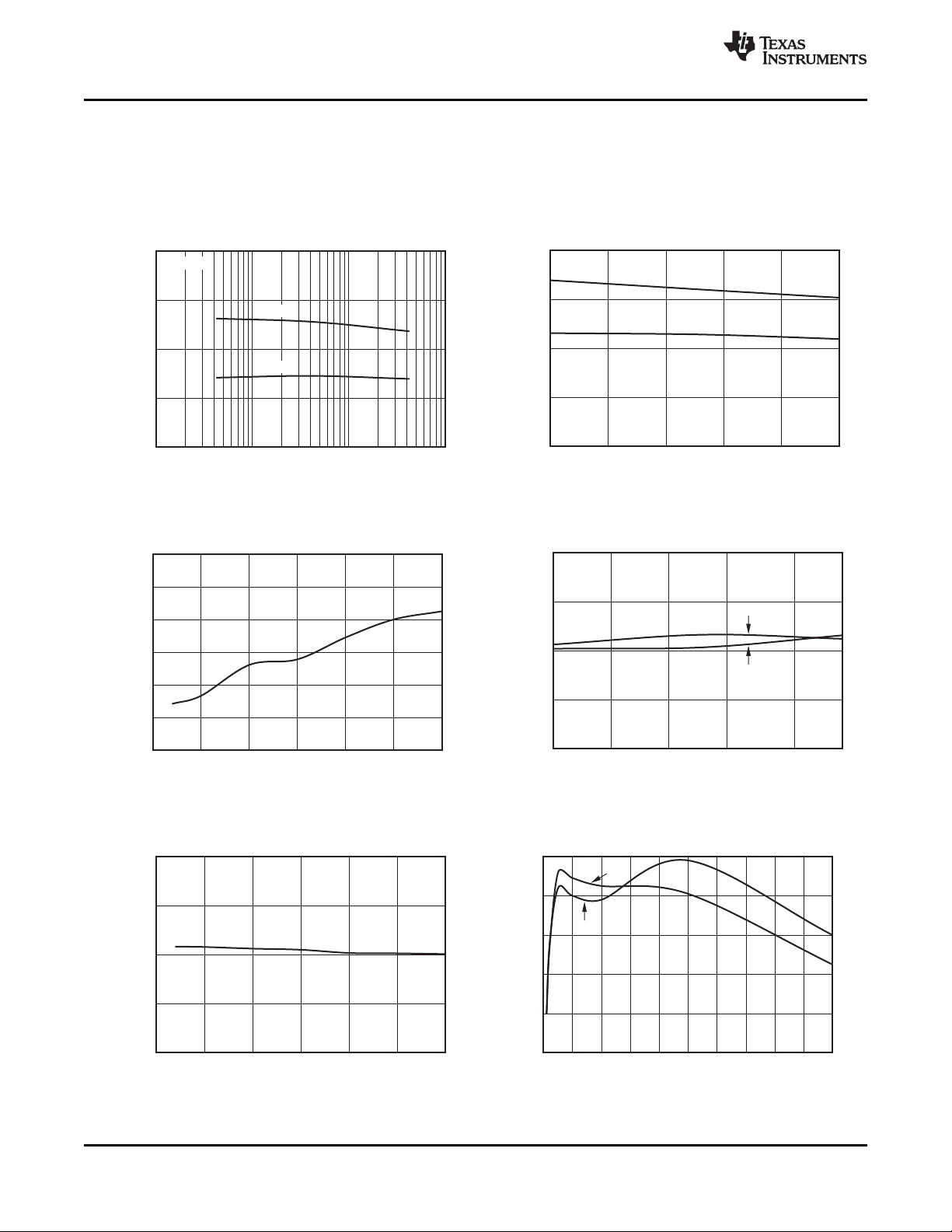
INTEGRAL NONLINEARITY OFFSET VOLTAGE
Figure 12. Figure 13.
OFFSET VOLTAGE GAIN ERROR
vs SUPPLY VOLTAGE vs FREE-AIR TEMPERATURE
[(REF+) – (REF – )] = 2.5V when +VA =
REF
www.ti.com
16 Submit Documentation Feedback Copyright © 2008 – 2009, Texas Instruments Incorporated
Figure 14. Figure 15.
GAIN ERROR POWER-SUPPLY REJECTION RATIO
vs SUPPLY VOLTAGE vs SUPPLY RIPPLE FREQUENCY
Figure 16. Figure 17.
Product Folder Link(s): ADS7229 ADS7230
 Loading...