

SAR-ADC
Oscillator and
Timing Control
I2C Interface
Conversion Result
ALERT
ADDR
SCL
SDA
AINP/AIN0
AINM/AIN1
AVDD
DVDD
GND
BUSY/RDY
Accumulator
Conversion Result [0]
«««.
Conversion Result [15]
Data Buffer
Analog Input and
Multiplexer
«««.
«««.
High/Low Threshold
± Hysteresis
Digital
Window
Comparator
I2C Address
Selector
Offset
Calibration
Product
Folder
Order
Now
Technical
Documents
Tools &
Software
Support &
Community
ADS7142-Q1
SBAS891A –NOVEMBER 2018–REVISED OCTOBER 2019
ADS7142-Q1 Automotive, 2-Channel, 12-Bit, 140-kSPS, I2C-Compatible ADC With
Programmable Threshold and Host Wake-Up Features
1 Features
1
• AEC-Q100 qualified for automotive applications:
– Device temperature grade 1:
–40°C to 125°C, T
• Small package size: 3 mm × 2 mm
• 12-bit noise-free resolution
• Up to 140-kSPS sampling rate
• Efficient host sleep and wake-up:
– Autonomous monitoring at 900 nW
– Windowed comparator for event-triggered host
wake-up
• Independent configuration and calibration:
– Dual-channel, pseudo-differential, or ground-
sense input configuration
– Programmable thresholds for calibration
– Internal calibration improves offset and drift
• False trigger prevention:
– Programmable thresholds per channel
– Programmable hysteresis for noise immunity
– Event counter for transient rejection
• I2C interface:
– Compatible from 1.65 V to 3.6 V
– 8 configurable addresses
– Up to 3.4 MHz (high speed)
• Analog supply: 1.65 V to 3.6 V
A
2 Applications
General-purpose voltage, current and temperature
monitoring in:
• Automotive camera modules
• Driver monitoring and assistance systems
• Infotainment systems and clusters
• Electric and ICE powertrain systems
3 Description
The ADS7142-Q1 is 12-bit, 140-kSPS successiveapproximation register (SAR) analog-to-digital
converter (ADC) that can autonomously monitor
signals while maximizing system power, reliability,
and performance. The device implements eventtriggered interrupts per channel using a digital
window comparator with programmable high and low
thresholds, hysteresis, and event counter. The device
includes a dual-channel analog multiplexer in front of
a SAR ADC followed by an internal data buffer for
converting and capturing data from sensors.
The ADS7142-Q1 is available in a 10-pin WSON
package and can achieve low power consumption of
only 900 nW. The small form-factor and low-power
consumption make this device suitable for spaceconstrained applications.
Device Information
PART NAME PACKAGE BODY SIZE (NOM)
ADS7142-Q1 WSON (10) 3.00 mm × 2.00 mm
(1) For all available packages, see the orderable addendum at
the end of the datasheet.
(1)
1
Block Diagram
An IMPORTANT NOTICE at the end of this data sheet addresses availability, warranty, changes, use in safety-critical applications,
intellectual property matters and other important disclaimers. PRODUCTION DATA.

ADS7142-Q1
SBAS891A –NOVEMBER 2018–REVISED OCTOBER 2019
www.ti.com
Table of Contents
1 Features.................................................................. 1
2 Applications ........................................................... 1
3 Description ............................................................. 1
4 Revision History..................................................... 2
5 Pin Configuration and Functions......................... 3
6 Specifications......................................................... 4
6.1 Absolute Maximum Ratings ...................................... 4
6.2 ESD Ratings.............................................................. 4
6.3 Recommended Operating Conditions....................... 4
6.4 Thermal Information.................................................. 4
6.5 Electrical Characteristics: All Modes......................... 5
6.6 Electrical Characteristics: Manual Mode................... 6
6.7 Electrical Characteristics: Autonomous Modes......... 7
6.8 Electrical Characteristics: High Precision Mode ....... 8
6.9 Timing Requirements................................................ 8
6.10 Switching Characteristics...................................... 10
6.11 Typical Characteristics: All Modes........................ 12
6.12 Typical Characteristics: Manual Mode.................. 13
6.13 Typical Characteristics: Autonomous Modes........ 17
6.14 Typical Characteristics: High-Precision Mode ...... 18
7 Detailed Description............................................ 19
4 Revision History
7.1 Overview................................................................. 19
7.2 Functional Block Diagram....................................... 19
7.3 Feature Description................................................. 20
7.4 Device Functional Modes........................................ 28
7.5 Programming........................................................... 39
7.6 Register Map........................................................... 42
8 Application and Implementation ........................ 59
8.1 Application Information............................................ 59
8.2 Typical Applications ................................................ 59
9 Power Supply Recommendations...................... 65
9.1 AVDD and DVDD Supply Recommendations......... 65
10 Layout................................................................... 66
10.1 Layout Guidelines ................................................. 66
10.2 Layout Example .................................................... 67
11 Device and Documentation Support................. 68
11.1 Receiving Notification of Documentation Updates 68
11.2 Community Resources.......................................... 68
11.3 Trademarks........................................................... 68
11.4 Electrostatic Discharge Caution............................ 68
11.5 Glossary................................................................ 68
12 Mechanical, Packaging, and Orderable
Information........................................................... 68
Changes from Original (November 2018) to Revision A Page
• Changed document status from advance information to production data.............................................................................. 1
2
Submit Documentation Feedback Copyright © 2018–2019, Texas Instruments Incorporated
Product Folder Links: ADS7142-Q1
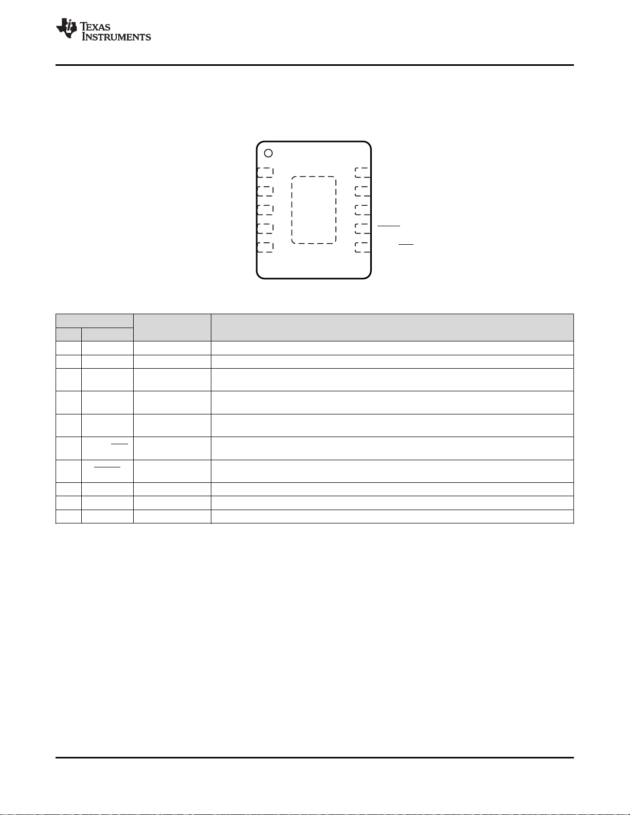
1GND 10 DVDD
2AVDD 9 SCL
3AINP/AIN0 8 SDA
4AINM/AIN1 7 ALERT
5ADDR 6 BUSY/RDY
Not to scale
Thermal
Pad
ADS7142-Q1
www.ti.com
SBAS891A –NOVEMBER 2018–REVISED OCTOBER 2019
5 Pin Configuration and Functions
DQC Package
10-Pin WSON
Top View
Pin Functions
PIN
NO. NAME
1 GND Supply Ground for power supply, all analog and digital signals are referred to this pin.
2 AVDD Supply Analog supply input, also used as the reference voltage for analog-to-digital conversion.
3 AINP/AIN0 Analog input
4 AINM/AIN1 Analog input
5 ADDR Analog Input
6 BUSY/RDY Digital output
7 ALERT Digital output
8 SDA Digital input/output Serial data input/output for the I2C interface. Connect a pullup resistor from DVDD to this pin.
9 SCL Digital input Serial clock for the I2C interface. Connect a pullup resistor from DVDD to this pin.
10 DVDD Supply Digital I/O supply voltage.
I/O DESCRIPTION
Single-channel operation: positive analog signal input.
Two-channel operation: analog signal input, channel 0.
Single-channel operation: negative analog signal input.
Two-channel operation: analog signal input, channel 1.
Input for selecting the I2C address of the device.
See the I2C Address Selection section for details.
The device pulls this pin high when scanning through channels in a sequence and brings this pin
low when the sequence is completed or aborted.
Active low, open-drain output. The status of this pin is controlled by the digital window
comparator block. Connect a pullup resistor from DVDD to this pin.
Product Folder Links: ADS7142-Q1
Submit Documentation FeedbackCopyright © 2018–2019, Texas Instruments Incorporated
3
ADS7142-Q1
SBAS891A –NOVEMBER 2018–REVISED OCTOBER 2019
www.ti.com
6 Specifications
6.1 Absolute Maximum Ratings
over operating free-air temperature range (unless otherwise noted)
ADDR to GND –0.3 AVDD + 0.3 V
AVDD to GND –0.3 3.9 V
DVDD to GND –0.3 3.9 V
AINP/AIN0 to GND –0.3 AVDD + 0.3 V
AINM/AIN1 to GND –0.3 AVDD + 0.3 V
Input current on any pin except supply pins –10 10 mA
Digital input to GND –0.3 DVDD + 0.3 V
Junction temperature, T
Storage temperature, T
J
stg
(1) Stresses beyond those listed under Absolute Maximum Rating may cause permanent damage to the device. These are stress ratings
only, which do not imply functional operation of the device at these or any other conditions beyond those indicated under Recommended
Operating Condition. Exposure to absolute-maximum-rated conditions for extended periods may affect device reliability.
6.2 ESD Ratings
Human-body model (HBM), per AEC Q100-002
V
(ESD)
(1) AEC Q100-002 indicates that HBM stressing shall be in accordance with the ANSI/ESDA/JEDEC JS-001 specification.
Electrostatic discharge
Charged-device model (CDM), per AEC
Q100-011
(1)
MIN MAX UNIT
–40 150 °C
–60 150 °C
VALUE UNIT
(1)
Corner pins (1, 5, 6, and
10)
±2000
±750
V
All other pins ±500
6.3 Recommended Operating Conditions
over operating free-air temperature range (unless otherwise noted)
MIN NOM MAX UNIT
AVDD Analog supply voltage range 1.65 3.6 V
DVDD Digital supply voltage range 1.65 3.6 V
T
A
Ambient temperature –40 125 °C
6.4 Thermal Information
ADS7142-Q1
THERMAL METRIC
R
θJA
R
θJC(top)
R
θJB
Ψ
JT
Ψ
JB
R
θJC(bot)
Junction-to-ambient thermal resistance 61.8 °C/W
Junction-to-case (top) thermal resistance 66.3 °C/W
Junction-to-board thermal resistance 29.8 °C/W
Junction-to-top characterization parameter 2.1 °C/W
Junction-to-board characterization parameter 29.7 °C/W
Junction-to-case (bottom) thermal resistance 6.1 °C/W
(1) For more information about traditional and new thermal metrics, see the Semiconductor and IC Package Thermal Metrics application
report.
(1)
UNITDQC (WSON)
10 PINS
4
Submit Documentation Feedback Copyright © 2018–2019, Texas Instruments Incorporated
Product Folder Links: ADS7142-Q1
ADS7142-Q1
www.ti.com
SBAS891A –NOVEMBER 2018–REVISED OCTOBER 2019
6.5 Electrical Characteristics: All Modes
at TA= -40°C to 125°C, AVDD = 3 V, DVDD = 1.65 V to 3.6 V, All Channel Configurations (unless otherwise noted)
PARAMETER TEST CONDITIONS MIN TYP MAX UNIT
ANALOG INPUT (Two-Channel Single-Ended Configuration)
Full-scale input voltage
(1)
span
Absolute input voltage
range
ANALOG INPUT (Single-Channel Single-Ended Configuration with Remote Ground Sense)
Full-scale input voltage
(1)
span
Absolute input voltage
range
ANALOG INPUT (Single-Channel Pseudo-Differential Configuration with Remote Ground Sense)
Full-scale input voltage
(1)
span
Absolute input voltage
range
INTERNAL OSCILLATOR
t
HSO
t
LPO
Time period for highspeed oscillator
Time period for low-power
oscillator
DIGITAL INPUT/OUTPUT (SCL, SDA)
V
V
V
I
OL
I
OL
I
I
C
High-level input voltage 0.7 × DVDD DVDD V
IH
Low-level input voltage 0 0.3 × DVDD V
IL
Low-level output voltage
OL
Low-level output current
(sink)
Low-level output current
(sink)
Input current on pin 10 µA
Input capacitance on pin 10 pF
I
DIGITAL OUTPUT (BUSY/RDY)
V
V
High-level output voltage I
OH
Low-level output voltage I
OL
DIGITAL OUTPUT (ALERT)
I
OL
V
Low-level output current VOL< 0.25 V 5 mA
Low-level output voltage I
OL
POWER-SUPPLY REQUIREMENTS
AVDD Analog supply voltage 1.65 3.6 V
DVDD Digital I/O supply voltage 1.65 3.6 V
(1) Ideal Input span, does not include gain or offset error.
AINP/AIN0 to GND or AINM/AIN1 to GND 0 AVDD V
AINP/AIN0 to GND or AINM/AIN1 to GND –0.1 AVDD + 0.1 V
AINP/AIN0 to AINM/AIN1 0 AVDD V
AINP/AIN0 to GND –0.1 AVDD + 0.1
AINM/AIN1 to GND –0.1 0.1
AINP/AIN0 to AINM/AIN1 –AVDD/2 AVDD/2 V
AINP/AIN0 to GND –0.1 AVDD + 0.1
AINM/AIN1 to GND AVDD/2–0.1 AVDD/2+0.1
50 110 ns
95.2 300 µs
With 3 mA sink current and DVDD > 2 V 0 0.4
With 3 mA sink current and 1.65 V < DVDD <
2 V
VOL= 0.4 V for standard and fast mode (100,
400 kHz)
0 0.2 × DVDD
3
VOL= 0.6 V for fast mode (400 kHz) 6
VOL= 0.4 V fast mode Plus (1 MHz) 20
VOL= 0.4 V high speed (1.7 MHz, 3.4 MHz) 25 mA
= 2 mA 0.7 × DVDD DVDD V
source
= 2 mA 0 0.3 × DVDD V
sink
= 5 mA 0 0.25 V
sink
(1)
V
V
V
mA
Product Folder Links: ADS7142-Q1
Submit Documentation FeedbackCopyright © 2018–2019, Texas Instruments Incorporated
5
ADS7142-Q1
SBAS891A –NOVEMBER 2018–REVISED OCTOBER 2019
www.ti.com
6.6 Electrical Characteristics: Manual Mode
at TA= -40°C to 125°C, AVDD = 3 V, DVDD = 1.65 V to 3.6 V, All Channel Configurations (unless otherwise noted)
PARAMETER TEST CONDITIONS MIN TYP MAX UNIT
SAMPLING DYNAMICS
t
conv
t
acq
t
cycle
DC SPECIFICATIONS
NMC No missing codes AVDD = 1.65 V to 3.6 V 12 Bits
DNL Differential nonlinearity AVDD = 1.65 V to 3.6 V –0.99 ±0.3 1 LSB
INL Integral nonlinearity –2.75 ±0.5 2.75 LSB
E
O
dVOS/dT Offset drift with temperature Post offset calibration 5 ppm/°C
E
G
AC SPECIFICATIONS
(2)
SNR
(2)(3)
THD
SINAD
SFDR
BW –3-dB small-signal bandwidth 25 MHz
POWER CONSUMPTION
I
AVDD
I
DVDD
I
AVDD
I
DVDD
(1) LSB means least significant byte. See the ADC Transfer Function for details.
(2) All specifications expressed in decibels (dB) refer to the full-scale input (FSR) and are tested with an input signal 0.5 dB below full-scale,
unless otherwise specified.
(3) Calculated on the first nine harmonics of the input frequency.
Conversion time AVDD = 1.65 V to 3.6 V 1.8 µs
Acquisition time AVDD = 1.65 V to 3.6 V 18 T
Cycle time AVDD = 1.65 V to 3.6 V, SCL = 3.4 MHz 7.1 µs
Resolution 12 Bits
Offset error Post offset calibration –4 ±0.5 4 LSB
Gain error –0.1 ±0.03 0.1 %FSR
Gain error drift with
temperature
Signal-to-noise ratio
Total harmonic distortion
(2)
Signal-to-noise and distortion
(2)
Spurious-free dynamic range
Analog supply current
Digital supply current
fIN= 2 kHz, AVDD = 3 V,
f
= 140 kSPS
SAMPLE
68.75 70
fIN= 2 kHz, AVDD = 1.8 V,
f
= 140 kSPS
SAMPLE
fIN= 2 kHz, AVDD = 3 V,
f
= 140 kSPS
SAMPLE
fIN= 2 kHz, AVDD = 1.8 V,
f
= 140 kSPS
SAMPLE
fIN= 2 kHz, AVDD = 3 V,
f
= 140 kSPS
SAMPLE
68.5 69.5
fIN= 2 kHz, AVDD = 1.8 V,
f
= 140 kSPS
SAMPLE
fIN= 2 kHz, AVDD = 3 V,
f
= 140 kSPS
SAMPLE
f
= 140 kSPS, SCL = 3.4 MHz 265 300
SAMPLE
f
= 5.5 kSPS, SCL = 100 kHz 8
SAMPLE
f
= 140 kSPS, SCL = 3.4 MHz, AVDD
SAMPLE
= 1.8 V
f
= 5.5 kSPS, SCL = 100 kHz, AVDD
SAMPLE
= 1.8 V
f
= 140 kSPS, SCL = 3.4 MHz, SDA =
SAMPLE
AAA0h
f
= 5.5 kSPS, SCL = 100 kHz, SDA =
SAMPLE
AAA0h
f
= 140 kSPS, SCL = 3.4 MHz, AVDD
SAMPLE
= 1.8 V, SDA = AAA0h
5 ppm/°C
68
–85
–80
67.5
90 dB
160
5
25
2
15
Static analog supply current No activity on SCL and SDA 6 nA
Static digital supply current No activity on SCL and SDA 2 nA
(1)
SCL
(1)
dB
dB
dB
µA
µA
6
Submit Documentation Feedback Copyright © 2018–2019, Texas Instruments Incorporated
Product Folder Links: ADS7142-Q1
ADS7142-Q1
www.ti.com
SBAS891A –NOVEMBER 2018–REVISED OCTOBER 2019
6.7 Electrical Characteristics: Autonomous Modes
at TA= -40°C to 125°C, AVDD = 3 V, DVDD = 1.65 V to 3.6 V, All Channel Configurations (unless otherwise noted)
PARAMETER TEST CONDITIONS MIN TYP MAX UNIT
SAMPLING DYNAMICS
t
conv
t
acq
t
cycle
Conversion time
Acquisition time
Cycle time
DC SPECIFICATIONS
Resolution 12 Bits
E
E
Offset error Post offset calibration ±0.5 LSB
O
Gain error ±0.03 %FSR
G
POWER CONSUMPTION
I
AVDD
I
DVDD
I
AVDD
I
DVDD
Analog supply current
Digital supply current
Static analog supply current No activity on SCL and SDA 5 nA
Static digital supply current No activity on SCL and SDA 0.6 nA
High-speed oscillator 14 t
Low-power oscillator 14 t
High-speed oscillator 7 t
Low-power oscillator 4 t
High-speed oscillator nCLK t
Low-power oscillator nCLK t
With low-power oscillator, nCLK = 18 0.75
With low-power oscillator, AVDD = 1.8 V,
nCLK = 18
0.45
With low-power oscillator, nCLK = 250 0.5
With low-power oscillator, nCLK = 21 940
With low-power oscillator, nCLK = 18, DVDD
= 3.3 V
With low-power oscillator, DVDD = 1.8 V,
nCLK = 18
With low-power oscillator, nCLK = 250,
DVDD = 3.3 V
With high-power oscillator, nCLK = 21,
DVDD = 3.3 V
0.15
0.25
0.15
0.15
HSO
LPO
HSO
LPO
HSO
LPO
µA
µA
Product Folder Links: ADS7142-Q1
Submit Documentation FeedbackCopyright © 2018–2019, Texas Instruments Incorporated
7
ADS7142-Q1
SBAS891A –NOVEMBER 2018–REVISED OCTOBER 2019
6.8 Electrical Characteristics: High Precision Mode
at TA= -40°C to 125°C, AVDD = 3 V, DVDD = 1.65 V to 3.6 V, All Channel Configurations (unless otherwise noted)
PARAMETER TEST CONDITIONS MIN TYP MAX UNIT
DC SPECIFICATIONS
Resolution
ENOB Effective number of bits With DC input of AVDD / 2
E
E
Offset error Post offset calibration ±10 LSB
O
Gain error ±0.03 %FSR
G
POWER CONSUMPTION
I
AVDD
I
DVDD
I
AVDD
I
DVDD
Analog supply current
Digital supply current
Static analog supply current No activity on SCL and SDA 5 nA
Static analog supply current No activity on SCL and SDA 0.7 nA
(1) Sampling dynamics for high precision mode are same as for autonomous modes.
(2) See Equation 5
(3) For DC input, ENOB = Ln[FSR/Standard deviation of Codes]/Ln[2]. See
(2)
(3)
16
15.4
With low-power oscillator, nCLK = 18 0.6
With low-power oscillator, AVDD = 1.8 V,
nCLK = 18
0.3
With low-power oscillator, nCLK = 250 0.5
With high-speed oscillator, nCLK = 21 980
With low-power oscillator, nCLK = 21, DVDD
= 3.3 V
With low-power oscillator, DVDD = 1.8 V,
nCLK = 21
With low-power oscillator, nCLK = 250,
DVDD = 3.3 V
With high-speed oscillator, nCLK = 21,
DVDD = 3.3 V
0.2
0.25
0.2
0.2
www.ti.com
(1)
Bits
µA
µA
6.9 Timing Requirements
at TA= -40°C to 125°C, AVDD = 3 V, DVDD = 1.65 V to 3.6 V, All Channel Configurations (unless otherwise noted)
PARAMETER MIN MAX UNIT
STANDARD MODE (100 kHz)
f
SCL
t
HD-STA
t
LOW
t
HIGH
t
SU-STA
(2)(3)
t
HD-DAT
t
SU-DAT
t
SU-STO
t
BUF
C
b
FAST MODE (400 kHz)
f
SCL
t
HD-STA
t
LOW
t
HIGH
(1) All values referred to V
(2) t
(3) The maximum t
8
is the data hold time that is measured from the falling edge of SCL and applies to data in transmission and the acknowledge.
HD-DAT
t
by a transition time. This maximum must only be met if the device does not stretch the LOW period (t
VD-ACK
the clock is streched, the data must be valid by the setup time before being released.
Submit Documentation Feedback Copyright © 2018–2019, Texas Instruments Incorporated
SCL clock frequency 0 100 kHz
Hold time (repeated) START condition 4 µs
Low period of SCL 4.7 µs
High period of SCL 4 µs
Setup time for a repeated start condition 4.7 µs
Data hold time 0 µs
Data setup time 250 ns
Data setup time 4 µs
Bus free time between a STOP and START
condition
4.7 µs
Capacitive load on each line 400 pF
SCL clock frequency 0 400 kHz
Hold time (repeated) START condition 0.6 µs
Low period of SCL 1.3 µs
High period of SCL 0.6 µs
(0.7 DVDD) and V
IH(min)
can be 3.45 µs and 0.9 µs for standard-mode and fast-mode, but must be less than the maximum of t
HD-DAT
IL(max)
(0.3 DVDD).
) of the SCL signal. If
LOW
Product Folder Links: ADS7142-Q1
(1)
VD-DAT
or
ADS7142-Q1
www.ti.com
SBAS891A –NOVEMBER 2018–REVISED OCTOBER 2019
Timing Requirements (continued)
at TA= -40°C to 125°C, AVDD = 3 V, DVDD = 1.65 V to 3.6 V, All Channel Configurations (unless otherwise noted)
PARAMETER MIN MAX UNIT
t
SU-STA
t
HD-DAT
t
SU-DAT
t
SU-STO
t
BUF
C
b
FAST MODE PLUS (1000 kHz)
f
SCL
t
HD-STA
t
LOW
t
HIGH
t
SU-STA
t
HD-DAT
t
SU-DAT
t
SU-STO
t
BUF
C
b
HIGH SPEED MODE (1.7 MHz, Cb= 400 pF max)
f
SCLH
t
HD-STA
t
LOW
t
HIGH
t
SU-STA
t
HD-DAT
t
SU-DAT
t
SU-STO
C
b
HIGH SPEED MODE (3.4 MHz, Cb= 100 pF max)
f
SCLH
t
HD-STA
t
LOW
t
HIGH
t
SU-STA
t
HD-DAT
t
SU-DAT
t
SU-STO
C
b
Setup time for a repeated start condition 0.6 µs
Data hold time 0 µs
Data setup time 100 ns
Data setup time 0.6 µs
Bus free time between a STOP and START
condition
1.3 µs
Capacitive load on each line 400 pF
SCL clock frequency 0 1000 kHz
Hold time (repeated) START condition 0.26 µs
Low period of SCL 0.5 µs
High period of SCL 0.26 µs
Setup time for a repeated start condition 0.26 µs
Data hold time 0 µs
Data setup time 50 ns
Data setup time 0.26 µs
Bus free time between a STOP and START
condition
0.5 µs
Capacitive load on each line 550 pF
SCLH clock frequency 0 1.7 MHz
Hold time (repeated) START condition 160 ns
Low period of SCL 320 ns
High period of SCL 120 ns
Setup time for a repeated start condition 160 ns
Data hold time 0 150 ns
Data setup time 10 ns
Data setup time 160 ns
Capacitive load on each line 100 pF
SCLH clock frequency 0 3.4 MHz
Hold time (repeated) START condition 160 ns
Low period of SCL 160 ns
High period of SCL 60 ns
Setup time for a repeated start condition 160 ns
Data hold time 0 70 ns
Data setup time 10 ns
Data setup time 160 ns
Capacitive load on each line 100 pF
(1)
Product Folder Links: ADS7142-Q1
Submit Documentation FeedbackCopyright © 2018–2019, Texas Instruments Incorporated
9
ADS7142-Q1
SBAS891A –NOVEMBER 2018–REVISED OCTOBER 2019
6.10 Switching Characteristics
at TA= -40°C to 125°C, AVDD = 3 V, DVDD = 1.65 V to 3.6 V, All Channel Configurations (unless otherwise noted)
PARAMETER TEST CONDITIONS MIN MAX UNIT
STANDARD MODE (100 kHz)
t
rCL
t
rDA
t
fCL
t
fDA
(2)
t
VD-DAT
(2)
t
VD-ACK
FAST MODE (400 kHz)
t
rCL
t
rDA
t
fCL
t
fDA
t
VD-DAT
t
VD-ACK
(3)
t
SP
FAST MODE PLUS (1000 kHz)
t
rCL
t
rDA
t
fCL
t
fDA
t
VD-DAT
t
VD-ACK
t
SP
HIGH SPEED MODE (1.7 MHz, Cb= 400 pF max)
t
rCL
t
rCL1
t
rDA
t
fCL
t
fDA
t
SP
HIGH SPEED MODE (3.4 MHz, Cb= 100 pF max)
t
rCL
t
rCL1
t
rDA
t
fCL
t
fDA
t
SP
Rise time of SCL 1000 ns
Rise time of SDA 1000 ns
Fall time of SCL 300 ns
Fall time of SDA 300 ns
Data valid time 3.45 µs
Data hold time 3.45 µs
Rise time of SCL 20 300 ns
Rise time of SDA 20 300 ns
Fall time of SCL 20 × DVDD/3.6 300 ns
Fall time of SDA 20 × DVDD/3.6 300 ns
Data valid time 0.9 µs
Data hold time 0.9 µs
Pulse duration of spikes suppressed by the
input filter
0 50 ns
Rise time of SCL 120 ns
Rise time of SDA 120 ns
Fall time of SCL 20 × DVDD/3.6 120 ns
Fall time of SDA 20 × DVDD/3.6 120 ns
Data valid time 0.45 µs
Data hold time 0.45 µs
Pulse duration of spikes suppressed by the
input filter
0 50 ns
Rise time of SCLH 20 80 ns
Rise time of SCLH after a repeated start
condition and after an acknowledge bit
20 160 ns
Rise time of SDAH 20 160 ns
Fall time of SCLH 20 80 ns
Fall time of SDAH 20 160 ns
Pulse duration of spikes suppressed by the
input filter
0 10 ns
Rise time of SCLH 10 40 ns
Rise time of SCLH after a repeated start
condition and after an acknowledge bit
10 80 ns
Rise time of SDAH 10 80 ns
Fall time of SCLH 10 40 ns
Fall time of SDAH 10 80 ns
Pulse duration of spikes suppressed by the
input filter
0 10 ns
www.ti.com
(1)
(1) All values referred to V
(2) t
(3) Input filters on the SDA and SCL inputs suppress noise spikes of less than 50 ns.
10
= time for data signal from SCL LOW to SDA output.
VD-DAT
Submit Documentation Feedback Copyright © 2018–2019, Texas Instruments Incorporated
( 0.7 DVDD ) and V
IH(min)
IL(max)
( 0.3 DVDD ).
Product Folder Links: ADS7142-Q1
Sr
t
fDA
t
rDA
t
HD-DAT
t
SU-DAT
SDAH or SDA
t
SU-STA
t
HD-STA
SCLH or SCL
t
rCL1
t
HIGH
t
LOW
t
FCL
t
rCL
t
LOW
t
HIGH
t
rCL1
t
SU-STO
Sr P
0.7 x V
DD
0.3 x V
DD
0.7 x V
DD
0.3 x V
DD
= MCS current source pull-up
= Rp resistor pull-up
(1)
(1)
t
f
t
r
t
SU-DAT
t
HD-DAT
t
VD-DAT
«
cont.
«
cont.
9th clock
SDA
SCL
70%
30%
70%
30%
70%
30% 30%
70%
70%
30%
70%
30%
t
HIGH
t
LOW
t
HD-STA
S
1/f
SCL
1st clock cycle
. . . SDA
. . . SCL
t
r
t
SU-STA
t
HD-STA
Sr
t
SP
t
VD-ACK
70%
30%
9th clock
t
BUF
S
P
t
SU-STO
VIL = 0.3V
DD
VIH = 0.7V
DD
t
f
www.ti.com
ADS7142-Q1
SBAS891A –NOVEMBER 2018–REVISED OCTOBER 2019
Figure 1. Timing Diagram for Standard Mode, Fast Mode, and Fast Mode Plus
(1) First rising edge of the SCLH signal after Sr and after each acknowledge bit.
Figure 2. Timing Diagram for High-Speed Mode
Product Folder Links: ADS7142-Q1
11
Submit Documentation FeedbackCopyright © 2018–2019, Texas Instruments Incorporated
Free-Air Temperature (qC)
Time Period (ns)
-40 -7 26 59 92 125
40
44
48
52
56
60
ADS7
Free-Air Temperature (qC)
Time Period (Ps)
-40 -7 26 59 92 125
60
80
100
120
140
160
ADS7
ADS7142-Q1
SBAS891A –NOVEMBER 2018–REVISED OCTOBER 2019
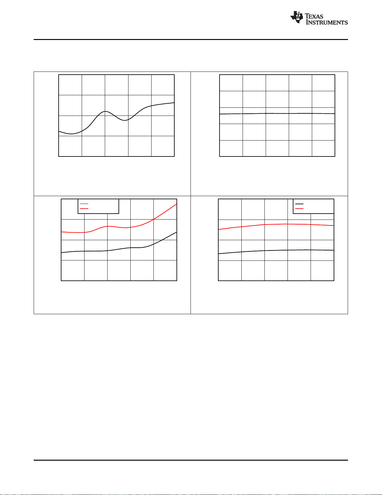
6.11 Typical Characteristics: All Modes
at TA= 25°C, AVDD = 3 V, DVDD = 3.3 V, and two-channel single-ended configuration (unless otherwise noted)
Figure 3. High-Speed Oscillator Time Period vs Temperature Figure 4. Low-Power Oscillator Time Period vs Temperature
www.ti.com
12
Submit Documentation Feedback Copyright © 2018–2019, Texas Instruments Incorporated
Product Folder Links: ADS7142-Q1
Free-Air Temperature (qC)
THD (dB)
-40 -7 26 59 92 125
-90
-88.4
-86.8
-85.2
-83.6
-82
ADS7
Free-Air Temperature (qC)
SFDR (dB)
-40 -7 26 59 92 125
88
88.6
89.2
89.8
90.4
91
ADS7
Free-Air Temperature (qC)
Amplitude (dB)
-40 -7 26 59 92 125
68
69
70
71
72
73
ADS7
SNR
SINAD
Free-Air Temperature (qC)
Amplitude (dB)
1.8 2.16 2.52 2.88 3.24 3.6
67
68
69
70
71
72
ADS7
SNR
SINAD
fIN, Input Frequency (Hz)
Amplitude (dB)
0 10000 20000 30000 40000 50000
-160
-140
-120
-100
-80
-60
-40
-20
0
ADS7
fIN, Input Frequency (Hz)
Amplitude (dB)
0 10000 20000 30000 40000 50000
-180
-160
-140
-120
-100
-80
-60
-40
-20
0
ADS7
www.ti.com
SBAS891A –NOVEMBER 2018–REVISED OCTOBER 2019
6.12 Typical Characteristics: Manual Mode
at TA= 25°C, AVDD = 3 V, DVDD = 3.3 V, and two-channel single-ended configuration (unless otherwise noted)
ADS7142-Q1
SNR = 69.6 dB, THD = –84 dB, ENOB = 11.2,
f
= 140 kSPS, SFDR = 87 dB, AVDD = 1.8 V
sample
Figure 5. Typical FFT in Manual Mode
f
= 140 kSPS
sample
Figure 7. SNR and SINAD in Manual Mode vs Temperature
SNR = 71.3 dB, THD = –87 dB, ENOB = 11.5,
f
= 140 kSPS, SFDR = 89.3 dB, AVDD = 3 V
sample
Figure 6. Typical FFT in Manual Mode
f
= 140 kSPS
sample
Figure 8. SNR and SINAD in Manual Mode vs AVDD
Figure 9. THD in Manual Mode vs Temperature
f
sample
= 140 kSPS
Figure 10. SFDR in Manual Mode vs Temperature
Product Folder Links: ADS7142-Q1
f
sample
Submit Documentation FeedbackCopyright © 2018–2019, Texas Instruments Incorporated
= 140 kSPS
13
Free-Air Temperature (qC)
Gain Error (FSR)
-40 -7 26 59 92 125
-0.05
-0.03
-0.01
0.01
0.03
0.05
ADS7
AVDD (V)
Gain Error (FSR)
1.8 2.16 2.52 2.88 3.24 3.6
-0.02
-0.002
0.016
0.034
0.052
0.07
ADS7
Free-Air Temperature (qC)
Offset Error (LSB)
-40 -7 26 59 92 125
1
1.4
1.8
2.2
2.6
3
ADS7
AVDD (V)
Offset Error (LSB)
1.8 2.16 2.52 2.88 3.24 3.6
0.5
0.9
1.3
1.7
2.1
2.5
ADS7
AVDD (V)
THD (dB)
1.8 2.16 2.52 2.88 3.24 3.6
-93
-90
-87
-84
-81
-78
ADS7
Output Code
Number of Hits
0
20000
40000
60000
2047 2048 2049
3790
3046
ADS7
ADS7142-Q1
SBAS891A –NOVEMBER 2018–REVISED OCTOBER 2019
Typical Characteristics: Manual Mode (continued)
at TA= 25°C, AVDD = 3 V, DVDD = 3.3 V, and two-channel single-ended configuration (unless otherwise noted)
www.ti.com
f
= 140 kSPS
sample
Figure 11. THD in Manual Mode vs AVDD
Mean code = 2047.9, standard deviation = 0.32
Figure 12. Typical DC Code Spread in Manual Mode
Figure 13. Offset Error in Manual Mode vs Temperature Figure 14. Offset Error in Manual Mode vs AVDD
14
Figure 15. Gain Error in Manual Mode vs Free-Air
Temperature
Submit Documentation Feedback Copyright © 2018–2019, Texas Instruments Incorporated
Product Folder Links: ADS7142-Q1
Figure 16. Gain Error in Manual Mode vs AVDD
Free-Air Temperature (qC)
Differential Nonlinearity (LSB)
-40 -7 26 59 92 125
-1
-0.6
-0.2
0.2
0.6
1
ADS7
Maximum
Minimum
AVDD (V)
Differential Nonlinearity (LSB)
1.8 2.16 2.52 2.88 3.24 3.6
-1
-0.6
-0.2
0.2
0.6
1
ADS7
Maximum
Minimum
Output Code
Integral Nonlinearity (LSB)
0 819 1638 2457 3276 4095
-1.2
-0.6
0
0.6
1.2
ADS7
Output Code
Integral Nonlinearity (LSB)
0 819 1638 2457 3276 4095
-1
-0.6
-0.2
0.2
0.6
1
ADS7
Output Code
Differential Nonlinearity (LSB)
0 819 1638 2457 3276 4095
-0.5
-0.3
-0.1
0.1
0.3
0.5
ADS7
Output Code
Differential Nonlinearity (LSB)
0 819 1638 2457 3276 4095
-0.5
-0.3
-0.1
0.1
0.3
0.5
ADS7
www.ti.com
SBAS891A –NOVEMBER 2018–REVISED OCTOBER 2019
Typical Characteristics: Manual Mode (continued)
at TA= 25°C, AVDD = 3 V, DVDD = 3.3 V, and two-channel single-ended configuration (unless otherwise noted)
ADS7142-Q1
AVDD = 3 V
Figure 17. Typical DNL in Manual Mode
AVDD = 3 V
Figure 19. Typical INL in Manual Mode
AVDD = 1.8 V
Figure 18. Typical DNL in Manual Mode
AVDD = 1.8 V
Figure 20. Typical INL in Manual Mode
Figure 21. DNL in Manual Mode vs Temperature Figure 22. DNL in Manual Mode vs AVDD
Product Folder Links: ADS7142-Q1
Submit Documentation FeedbackCopyright © 2018–2019, Texas Instruments Incorporated
15
SCL (kHz)
I
DVDD
(PA)
0 500 1000 1500 2000 2500 3000 3500
0
2.5
5
7.5
10
12.5
15
17.5
20
ADS7
Free-Air Temperature (qC)
I
AVDD
(PA)
-40 -7 26 59 92 125
-0.2
0
0.2
0.4
0.6
0.8
ADS7
AVDD = 1.8 V
AVDD = 3 V
AVDD (V)
I
AVDD
(PA)
1.8 2.16 2.52 2.88 3.24 3.6
100
150
200
250
300
350
ADS7
Free-Air Temperature (qC)
I
AVDD
(PA)
-40 -7 26 59 92 125
230
236
242
248
254
260
ADS7
Free-Air Temperature (qC)
Integral Nonlinearity (LSB)
-40 -7 26 59 92 125
-1.5
-1
-0.5
0
0.5
1
ADS7
Maximum
Minimum
AVDD (V)
Integral Nonlinearity (LSB)
1.8 2.16 2.52 2.88 3.24 3.6
-2
-1.4
-0.8
-0.2
0.4
1
ADS7
Maximum
Minimum
ADS7142-Q1
SBAS891A –NOVEMBER 2018–REVISED OCTOBER 2019
Typical Characteristics: Manual Mode (continued)
at TA= 25°C, AVDD = 3 V, DVDD = 3.3 V, and two-channel single-ended configuration (unless otherwise noted)
Figure 23. INL in Manual Mode vs Temperature Figure 24. INL in Manual Mode vs AVDD
www.ti.com
f
= 140 kSPS, SCL = 3.4 MHz
Sample
Figure 25. I
16
Figure 27. I
Submit Documentation Feedback Copyright © 2018–2019, Texas Instruments Incorporated
in Manual Mode vs AVDD Figure 26. I
AVDD
DVDD = 1.8 V
in Manual Mode vs SCL
DVDD
Figure 28. Static I
Product Folder Links: ADS7142-Q1
in Manual Mode vs Temperature
AVDD
No activity on SCL and SDA
in Manual Mode vs Temperature
AVDD
Free-Air Temperature (qC)
I
AVDD
(nA)
-40 -7 26 59 92 125
0
300
600
900
1200
1500
ADS7
AVDD = 1.8 V
AVDD = 3 V
Free-Air Temperature (qC)
I
AVDD
(PA)
-40 -7 26 59 92 125
0
300
600
900
1200
1500
Auto
AVDD = 1.8 V
AVDD = 3 V
nCLK
Analog Input Current (PA)
0 45 90 135 180 225 270
0
3
6
9
12
ADS7
nCLK
Analog Input Current (nA)
0 45 90 135 180 225 270
0
1.6
3.2
4.8
6.4
8
AINC
www.ti.com
SBAS891A –NOVEMBER 2018–REVISED OCTOBER 2019
6.13 Typical Characteristics: Autonomous Modes
at TA= 25°C, AVDD = 3 V, DVDD = 3.3 V, and two-channel single-ended configuration (unless otherwise noted)
ADS7142-Q1
Input voltage = 1.5 V, CH0, high-speed oscillator, stop burst mode
Figure 29. Analog Input Current in Autonomous Modes vs
nCLK
Stop burst mode, low-power oscillator, nCLK = 25
Figure 31. I
in Autonomous Modes vs Temperature
AVDD
Input voltage = 1.5 V, CH0, low-power oscillator, stop burst mode
Figure 30. Analog Input Current in Autonomous Modes vs
nCLK
Stop burst mode, high-speed oscillator, nCLK = 25
Figure 32. I
in Autonomous Modes vs Temperature
AVDD
Product Folder Links: ADS7142-Q1
Submit Documentation FeedbackCopyright © 2018–2019, Texas Instruments Incorporated
17
Free-Air Temperature (qC)
I
AVDD
(nA)
-40 -7 26 59 92 125
0
300
600
900
1200
ADS7
AVDD = 1.8 V
AVDD = 3 V
Free-Air Temperature (qC)
I
AVDD
(PA)
-40 -7 26 59 92 125
0
300
600
900
1200
AVDD = 1.8 V
AVDD = 3 V
Free-Air Temperature (qC)
Offset Error (LSB)
-40 -7 26 59 92 125
-2
1
4
7
10
Offs
Free-Air Temperature(qC)
Gain Error (FSR)
-40 -7 26 59 92 125
-0.03
-0.018
-0.006
0.006
0.018
0.03
Gain
ADS7142-Q1
SBAS891A –NOVEMBER 2018–REVISED OCTOBER 2019
6.14 Typical Characteristics: High-Precision Mode
at TA= 25°C, AVDD = 3 V, DVDD = 3.3 V, and two-channel single-ended configuration (unless otherwise noted)
www.ti.com
Figure 33. Offset Error in High-Precision Mode vs
Temperature
Low-power oscillator, nCLK = 25
Figure 35. I
in High-Precision Mode vs Temperature
AVDD
Figure 34. Gain Error in High-Precision Mode vs
Temperature
High-speed oscillator, nCLK = 25
Figure 36. I
in High-Precision Mode vs Temperature
AVDD
18
Submit Documentation Feedback Copyright © 2018–2019, Texas Instruments Incorporated
Product Folder Links: ADS7142-Q1
SAR-ADC
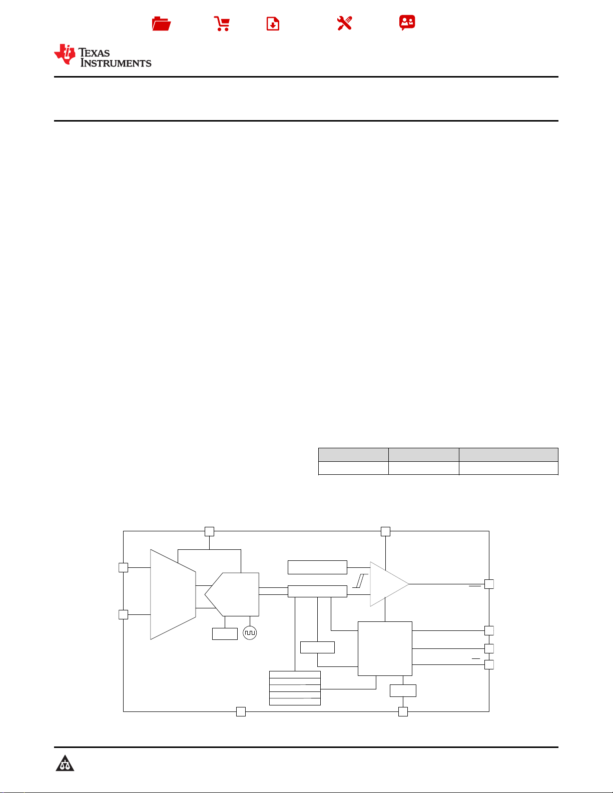
Oscillator and
Timing Control
I2C Interface
Conversion Result
ALERT
ADDR
SCL
SDA
AINP/AIN0
AINM/AIN1
AVDD
DVDD
GND
BUSY/RDY
Accumulator
Conversion Result [0]
«««.
Conversion Result [15]
Data Buffer
Analog Input and
Multiplexer
«««.
«««.
High/Low Threshold
± Hysteresis
Digital
Window
Comparator
I2C Address
Selector
Offset
Calibration
ADS7142-Q1
www.ti.com
SBAS891A –NOVEMBER 2018–REVISED OCTOBER 2019
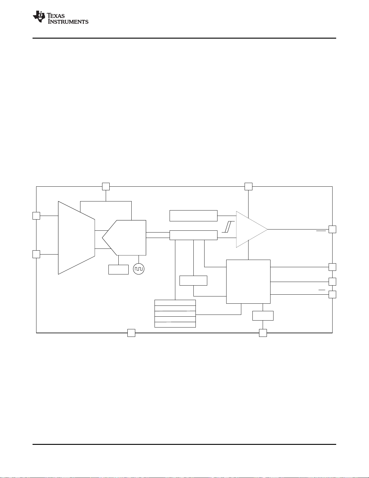
7 Detailed Description
7.1 Overview
The ADS7142-Q1 is a small size, dual-channel, 12-bit programmable sensor monitor with an integrated analogto-digital converter (ADC), input multiplexer, digital comparator, data buffer, accumulator and internal oscillator.
The input multiplexer can be either configured as two single-ended channels, one single-ended channel with
remote ground sensing, or one pseudo-differential channel where the input can swing to approximately AVDD /
2. The device includes a digital window comparator with a dedicated output pin, which can be used to alert the
host when a programmed high or low threshold is crossed. The device address is configured by the I2C address
selector block. The device uses internal oscillators (high speed or low power) for conversion. The start of
conversion is controlled by the host in manual mode and by the device in the autonomous modes.
The device also features a data buffer and an accumulator. The data buffer can store up to 16 conversion results
of the ADC in the autonomous modes and the accumulator can accumulate up to 16 conversion results of the
ADC in high-precision mode.
The device includes an offset calibration to calibration its own offset.
7.2 Functional Block Diagram
Product Folder Links: ADS7142-Q1
Submit Documentation FeedbackCopyright © 2018–2019, Texas Instruments Incorporated
19
AINP/AIN0
AINM/AIN1
AVDD
GND
GND + 100mV
GND -100mV
GND
C
s1
C
s
2
V_BIAS
SW
1
R
s1
R
s2
GND
SW
2
MUX
CHANNEL_INPUT_CFG_REG
AINP/AIN0
AINM/AIN1
AVDD
GND
AVDD/2 + 100mV
AVDD/2-100mV
AVDD/2
C
s1
C
s
2
V_BIAS
SW
1
R
s1
R
s2
GND
SW
2
MUX
CHANNEL_INPUT_CFG_REG
AVDD/2
C
s1
C
s
2
AVDD
AVDD
V_BIAS
AINP/AIN0
AINM/AIN1
SW
1
R
s1
R
s2
GND
SW
2
MUX
CHANNEL_INPUT_CFG_REG
AVDD
GND
AVDD
GND
CH0
CH1
C
s1
C
s
2
V_BIAS
AINP/AIN0
AINM/AIN1
SW
1
R
s
1
R
s2
GND
SW
2
MUX
CHANNEL_INPUT_CFG_REG
CH0
CH1
ADS7142-Q1
SBAS891A –NOVEMBER 2018–REVISED OCTOBER 2019
www.ti.com
7.3 Feature Description
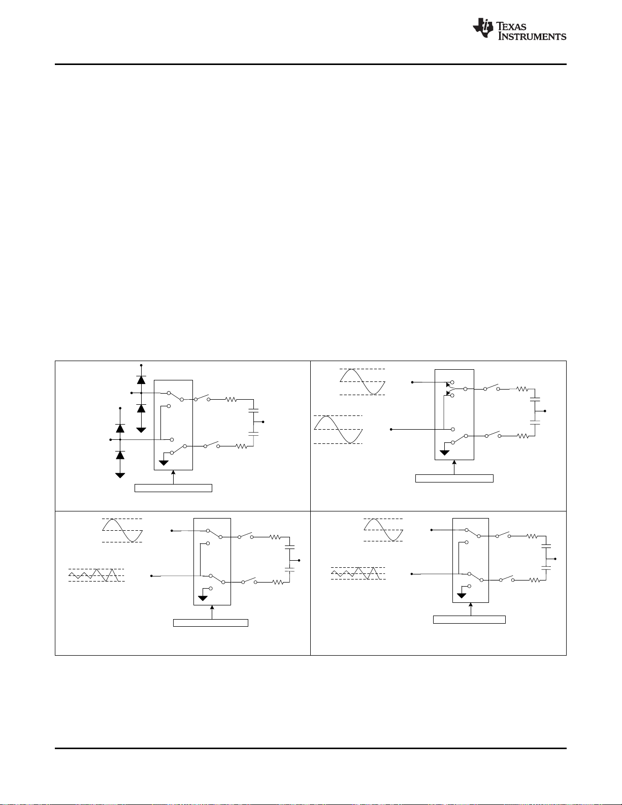
7.3.1 Analog Input and Multiplexer
Figure 37 shows a small-signal equivalent circuit for the analog input pins. The device includes a two-channel
analog multiplexer with each input pin having ESD protection diodes to AVDD and GND. The sampling switches
are represented by ideal switches SW1and SW2in series with resistors Rs1and Rs2(typically 150 Ω). The
sampling capacitors, Cs1and Cs2, are typically 15 pF. The multiplexer configuration is set by the
CH_INPUT_CFG register.
During acquisition, switches SW1and SW2are closed to allow the input signal to charge the internal sampling
capacitors.
During conversion, switches SW1and SW2are opened to disconnect the input signal from the sampling
capacitors.
The analog input of the device are optimized to be driven by high impedance source (up-to 100 kΩ) in
Autonomous Modes or in High Precision Mode mode with low power oscillator. It is recommended to drive the
analog input of the device with an external amplifier when in Autonomous Modes or in High Precision Mode
mode with a high-speed oscillator. Figure 29 and Figure 30 provide the analog input current for CH0 and CH1 of
the device.
Figure 38, Figure 39 and Figure 40 provide a simplified circuit for analog input for input configurations described
in Two-Channel, Single-Ended Configuration, Single-Channel, Single-Ended Configuration and Single-Channel,
Pseudo-Differential Configuration respectively. The analog multiplexer supports following input configurations (set
by writing into the CH_INPUT_CFG register).
Figure 37. Equivalent Circuit for Analog Input
Figure 38. Two-Channel, Single-Ended Configuration
Figure 39. Single-Channel, Single-Ended Configuration
With Remote Ground Sensing
7.3.1.1 Two-Channel, Single-Ended Configuration
Figure 38 shows a simplified block diagram showing a two-channel, single-ended configuration. Set the
CH0_CH1_IP_CFG bits = 00b or 11b to select this configuration. This configuration is also the default for the
device after power up. In this configuration, CS2always samples the GND pin and CS1samples the input signal
provided on channel 0 (AINP/AIN0) or channel 1 (AINM/AIN1) based on the channel selection. Each analog input
channel can accept input signals in the range 0 V to AVDD V.
20
Submit Documentation Feedback Copyright © 2018–2019, Texas Instruments Incorporated
Product Folder Links: ADS7142-Q1
Figure 40. Single-Channel, Pseudo-Differential
Configuration

ADS7142-Q1
www.ti.com
SBAS891A –NOVEMBER 2018–REVISED OCTOBER 2019
Feature Description (continued)
On power-up, the device wakes up in manual mode with two-channel, single-ended configuration and samples
CH0 only. This configuration can also be set by setting OPMODE_SEL to 000b or 001b,
The device can be configured to sample either CH0 or CH1 or both channels by setting bits in the
AUTO_SEQ_CHEN register to select the channels.
• To select a channel in AUTO sequence, set AUTO_SEQ_CHx bit in the AUTO_SEQ_CHEN register to 1.
• Set the bits in the OPMODE_SEL register to 100b or 101b for manual mode with AUTO sequence.
• Set the bits in the OPMODE_SEL register to 110b for Autonomous Modes with AUTO sequence.
• Set the bits in the OPMODE_SEL register to 111b for High Precision Mode with AUTO sequence.
7.3.1.2 Single-Channel, Single-Ended Configuration
See Figure 39 for a simplified block diagram showing a single-channel, single ended configuration. Set
CH0_CH1_IP_CFG bits = 01b to select this configuration. In this configuration, CS1samples the input signal
provided on the AINP/AIN0 pin whereas CS2samples input signal provided on the AINM/AIN1 pin. AINP/AIN0 pin
can accept input signals in the range 0 V to AVDD V and AINM/AIN1 pin can accept input signals in the range
–100 mV to +100 mV. This input configuration is useful in systems where the sensor and/or the signal
conditioning block is placed far from the device and there could be a small difference between the ground
potentials. In this channel configuration, remove channel 1 from AUTO sequence by setting the
AUTO_SEQ_CH1 bit to 0. Selecting channel 1 in AUTO sequence leads to an error condition and the device
sets an error flag in the SEQUENCE_STATUS register.
7.3.1.3 Single-Channel, Pseudo-Differential Configuration
See Figure 40 for a simplified block diagram showing a single-channel, pseudo-differential configuration. Set
CH0_CH1_IP_CFG bits = 10b to select this configuration. In this configuration, CS1samples the input signal
provided on the AINP/AIN0 pin whereas CS2samples input signal provided on the AINM/AIN1 pin. AINP/AIN0 pin
can accept input signals in the range 0 V to AVDD V and AINM/AIN1 pin can accept input signals in the range
(AVDD/2) - 100 mV to (AVDD/2) + 100 mV. This input configuration is useful to interface with sensors that
provide pseudo-differential signal with negative output as AVDD/2 like an electrochemical gas sensor. In this
channel configuration, remove channel 1 from AUTO sequence by setting the AUTO_SEQ_CH1 bit to 0.
Selecting channel 1 in AUTO sequence leads to an error condition and the device sets an error flag in
SEQUENCE_STATUS register.
7.3.2 OFFSET Calibration
The offset can be calibrated by setting the TRIG_OFFCAL bit in the OFFSET_CAL register. During offset
calibration, the sampling switches are open (Figure 37) and the device keeps BUSY/RDY pin high. The device
calculates its offset error and corrects for this error for subsequent conversions. The device calibrates the offset
on power up. To nullify the change in offset due to change in temperature or in AVDD voltage, it is recommended
to perform this calibration periodically.
7.3.3 Reference
The device uses the analog supply voltage (AVDD) as a reference for the analog-to-digital conversion process. It
is recommended to place a 220-nF, low-ESR ceramic decoupling capacitor between the AVDD pin and the GND
pin, close to the AVDD Pin. See Power Supply Recommendations section.
7.3.4 ADC Transfer Function
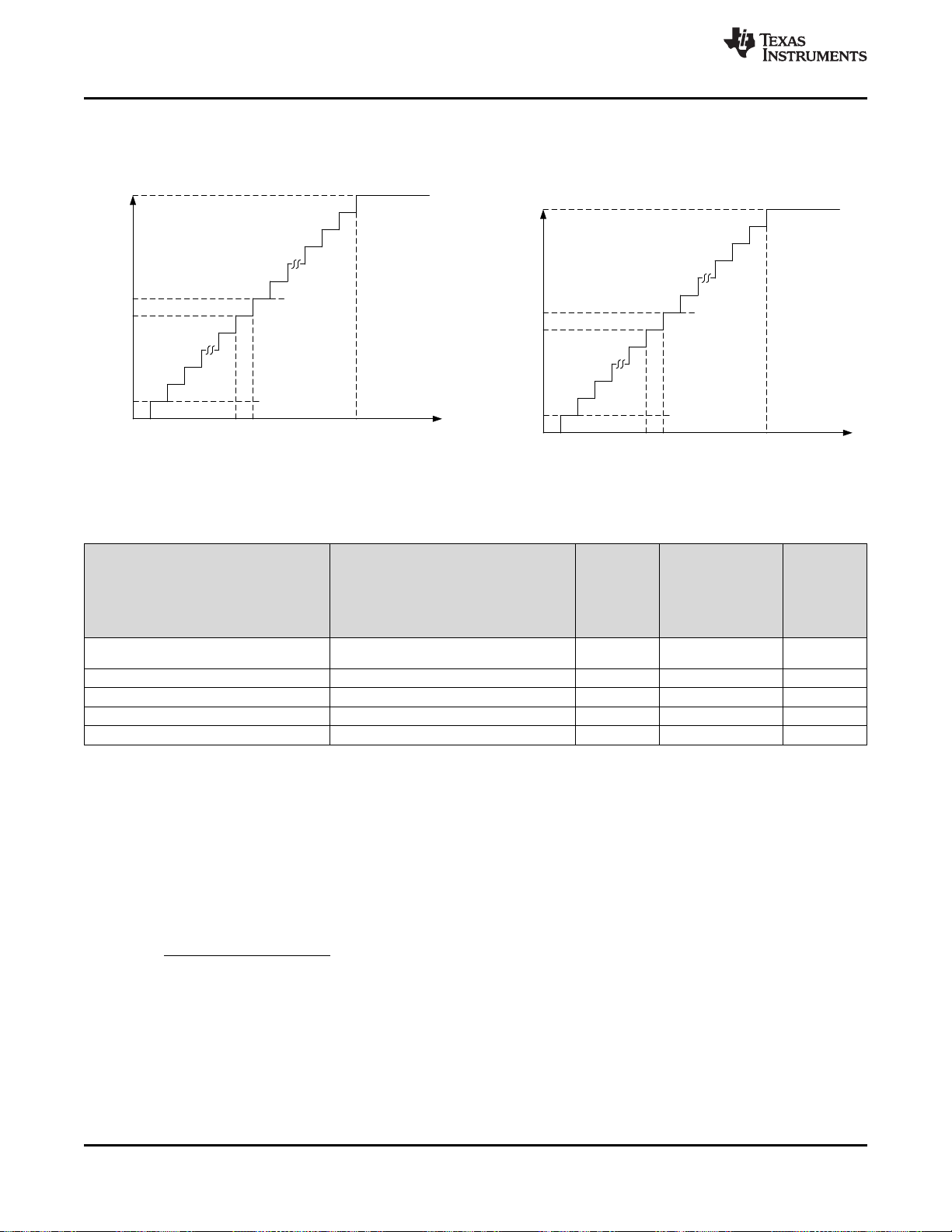
The ADC provides data in straight binary format. The ADC resolution can be computed by Equation 1:
1 LSB = V
REF
/ 2
N
where:
• V
• N = 12 for Autonomous Monitoring Modes and Manual Mode (1)
REF
= AVDD
Product Folder Links: ADS7142-Q1
Submit Documentation FeedbackCopyright © 2018–2019, Texas Instruments Incorporated
21
nCLK
frequencyOscillator
f
S
NFSC+1
PFSC
MC + 1
MC
ADC Code (Hex)
V
IN
NFSC
(V
REF
/2 ± 1 LSB)
1 LSB0(-V
REF
/2 + 1 LSB)
NFSC+1
PFSC
MC + 1
MC
ADC Code (Hex)
V
IN
NFSC
1 LSB
(V
REF
± 1 LSB)
(V
REF
/2 + 1 LSB)V
REF
/2
ADS7142-Q1
SBAS891A –NOVEMBER 2018–REVISED OCTOBER 2019
www.ti.com
Feature Description (continued)
Figure 41 and Figure 42 show the ideal transfer characteristics for single-ended input and pseudo-differential
input, respectively. Table 1 show the digital output codes for the transfer functions.
Figure 41. Ideal Transfer Characteristics for
Single-Ended Configurations
Figure 42. Ideal Transfer Characteristics for
Pseudo-Differential Configuration
Table 1. Transfer Characteristics
IDEAL
OUTPUT
INPUT VOLTAGE FOR SINGLE-ENDED INPUT
INPUT VOLTAGE FOR PSEUDO
DIFFERENTIAL INPUT
CODE DESCRIPTION
CODE
(Autonomous
Monitoring
Mode or
Manual Mode)
Negative full-scale
code
000
(V
REF
(V
/ 2) + 1 LSB to (V
REF
≤1 LSB ≤ (–V
1 LSB to 2 LSBs (–V
/ 2) to (V
≥ V
/ 2) + 1 LSB 0 LSB to 1 LSB MC Mid code 800
REF
/ 2) + 2 LSBs 1 LSB to 2 LSB MC + 1 — 801
REF
– 1 LSB ≥ V
REF
/ 2 + 1) to (–V
REF
/ 2 + 1) LSB NFSC
REF
/ 2 + 2) LSB NFSC + 1 — 001
REF
/ 2 – 1 LSB PFSC Positive full-scale code FFF
REF
7.3.5 Oscillator and Timing Control
The device uses one of the two internal oscillators (low power oscillator or high speed oscillator) for converting
the analog input voltage into a digital output code.
The steps for selecting the oscillator and setting the sampling speed are listed below:
1. Select the low power oscillator (OSC_SEL = 1b) to monitor slow moving signals (< 300 Hz) at extremely low
power consumption and sampling speeds (< 600 SPS). Select the high speed oscillator (OSC_SEL = 0b) to
scan the sensor signals with faster sampling speed (> 50 kHz).
2. Set sampling speed by programming the NCLK_SEL register:
22
• fs= Sampling speed
• Oscillator frequency = 1 / t
1 / t
HSO
or 1 / t
LPO
HSO
or 1 / t
depending on the OSC_SEL bit; see the Specifications section for
LPO
• nCLK is number of clocks in one conversion cycle (see the NCLK_SEL register) (2)
Submit Documentation Feedback Copyright © 2018–2019, Texas Instruments Incorporated
Product Folder Links: ADS7142-Q1
Copyright © 2017, Texas Instruments Incorporated
R1
R2
AVDD
ADDR
ADS7142-Q1
www.ti.com
SBAS891A –NOVEMBER 2018–REVISED OCTOBER 2019
7.3.6 I2C Address Selector
The I2C address for the device is determined by connecting external resistors on ADDR pin. The device address
are selected on power-up based on the resistor values. The device retains this address until the next power up,
or until next device reset, or until the device receives a command to program its own address (General Call With
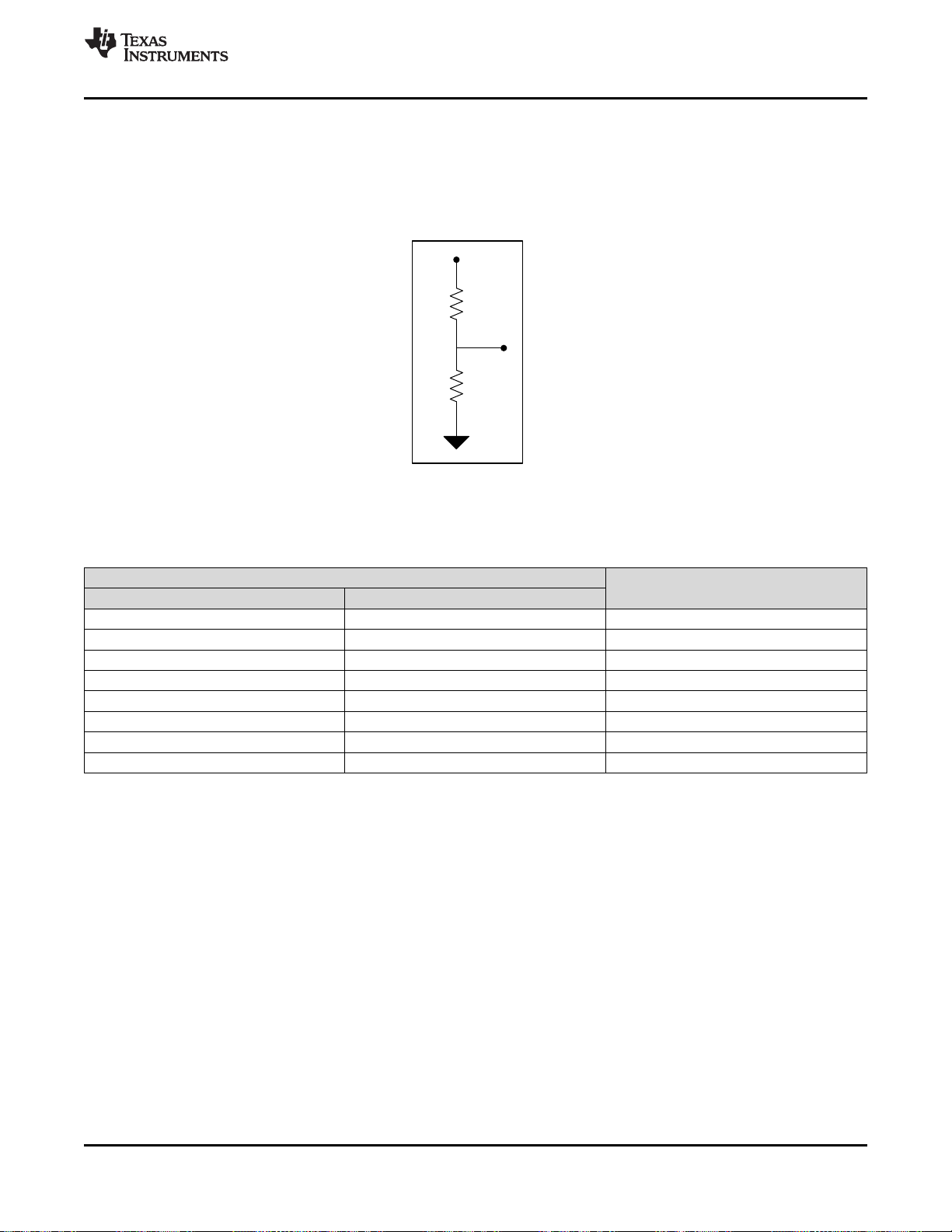
Write Software Programmable Part of Slave Address). Figure 43 provides the connection diagram for the ADDR
pin and Table 2 provides the resistor values for selecting different addresses of the device.
Figure 43. External Resistor Connection Diagram for ADDR Pin
Table 2. I2C Address Selection
(1)
R1
0 Ω DNP
11 kΩ DNP
33 kΩ DNP
100 kΩ DNP
(2)
DNP
(2)
DNP
(2)
DNP
(2)
DNP
(1) Tolerance for R1, R2 < ±5%.
(2) DNP = Do not populate.
RESISTORS
(1)
R2
(2)
(2)
(2)
(2)
0Ω or DNP
(2)
11 kΩ 0011001b (19h)
33 kΩ 0011010b (1Ah)
100 kΩ 0011011b (1Bh)
ADDRESS
0011111b (1Fh)
0011110b (1Eh)
0011101b (1Dh)
0011100b (1Ch)
0011000b (18h)
7.3.7 Data Buffer
When operating in autonomous monitoring mode, the device can use the internal data buffer for data storage.
The internal data buffer is 16-bit wide and 16-word deep and follows the first-in, first-out (FIFO) approach.
Product Folder Links: ADS7142-Q1
Submit Documentation FeedbackCopyright © 2018–2019, Texas Instruments Incorporated
23
Device Address (7 Bits) MSB for Data Buffer Entry 0 A LSB for Data Buffer Entry 0
LSB for Data Buffer Entry 15
R A A
P/Sr
Data from Host to Device
Data from Device to Host
S
N
MSB for Data Buffer Entry 1 A
ADS7142-Q1
SBAS891A –NOVEMBER 2018–REVISED OCTOBER 2019
www.ti.com
7.3.7.1 Filling of the Data Buffer
The write operation to the data buffer starts and stops as per the settings in the DATA_BUFFER_OPMODE
register. The DATA_BUFFER_STATUS register provides the number of entries filled in the data buffer and this
register can be read during an active sequence to get the current status of the data buffer.
The time between two consecutive conversions is set by the NCLK_SEL register and Equation 3 provides the
relationship for time between two consecutive conversions of the same channel and nCLK parameter.
tcc= k x nCLK x OscillatorTimePeriod
where
• tcc= Time between two consecutive conversions of same channel, tcc= k × t
• k = Number of channels enabled in the device sequence
• nCLK = Number of clocks used by device for one conversion cycle
• Oscillator timer period = t
or t
HSO
LPO
or t
depending on the OSC_SEL value; see the Specifications section for t
HSO
cycle
LPO
(3)
The format of the 16-bit contents of each entry in the data buffer are set by programming the
DOUT_FORMAT_CFG register. The DATA_OUT_CFG register enables the channel ID and DATA_VALID flag in
data buffer. Channel ID represents the channel number for the data entry in the data buffer. DATA_VALID is set
to zero in either of the following conditions:
• If the entry in the data buffer is not filled after the last start of sequence.
• If the I2C master tries to read more than 16 entries from the data buffer, the device provides zeros with
DATA_VALID set to zero
At the end of the write operation, the data buffer always has results of 16 (or lesser) consecutive conversions.
The data buffer is filled in the order that the data is converted by the ADC. The channels converted by the ADC
are controlled by the AUTO_SEQ_CHEN register. The entries that are not filled during an active sequence are
filled with zeros.
7.3.7.2 Reading Data From the Data Buffer
The device brings the BUSY/RDY pin low after completion of the sequence or after the SEQ_ABORT bit is set.
As illustrated in Figure 44, the device provides the contents of the data buffer (in FIFO fashion) on receiving I2C
read frame, which consists of the device address and the read bit set to 1.
Figure 44. Reading Data Buffer (16 Bit Words × 16 Words)
The device returns zeroes with DATA VALID flag set to zero for all I2C read frames received after all the valid
data words from the data buffer are read or when a I2C read frame is issued during an active sequence
(indicated by high on the BUSY/RDY pin). The I2C master needs to provide a NACK followed by a STOP or
RESTART condition in an I2C frame to finish the reading process. The data buffer is reset by setting the
SEQ_START bit or after resetting the device.
24
Submit Documentation Feedback Copyright © 2018–2019, Texas Instruments Incorporated
Product Folder Links: ADS7142-Q1

Conversion Result for CH0
(High Side Threshold, Hysteresis)
for CH0
(Low Side Threshold, Hysteresis)
for CH0
High Latched Flag for CH0
Low Latched Flag for CH0
High Side
Counter
Low Side
Counter
High Side Comparator
Low Side Comaparator
ADC
S
R
Q
R
S
Q
Write Bit to
Reset
OR
ALERT_EN_CH0
ALERT
End of
Conversion
OR
Channel 1
Channel 0
DWC_BLOCK_EN
ALERT_EN_CH1
16
2
AVDD
LSB
¦
16
1k
CHxfor Result[k]ConversionCHxfor DataPrecision High
ADS7142-Q1
www.ti.com
SBAS891A –NOVEMBER 2018–REVISED OCTOBER 2019
7.3.8 Accumulator
When operating in High Precision Mode, the device offers a 16-bit internal accumulator per channel. The
Accumulator for a channel is enabled only if that channel is selected in the channel scanning sequence. The
accumulator adds sixteen 12-bit conversion results. The result of adding 16 twelve bit words is one 16 bit word
that has an effective resolution of an 16-bit ADC. The time between two consecutive conversions for
accumulation is controlled by the NCLK_SEL register and Equation 3 provides the relationship for time between
two consecutive conversions of same channel and nCLK parameter.
The accumulated data can be read from the ACC_CHx_MSB and ACC_CHx_LSB registers in the device. The
ACCUMULATOR_STATUS register provides the number of accumulations done in the accumulator since last
conversion. This register can be read during an active sequence to get the current status of the accumulator.
The accumulator is reset on setting the SEQ_START bit and on resetting the device.
Equation 4 provides the relationship between high precision data and ADC conversion results.
(4)
Equation 5 provides the value of LSB in high precision mode for the accumulated result.
(5)
7.3.9 Digital Window Comparator
The internal digital window comparator is available in all modes. In Autonomous Modes with Thresholds
monitoring and Diagnostics, the digital window comparator controls the filling of the data and the output of the
alert pin and in other modes, it only controls the output of the ALERT pin. Figure 45 provides the block diagram
for digital window comparator.
Figure 45. Digital Comparator Block Diagram
The low side threshold, high side threshold, and hysteresis parameters are independently programmable for
each input channel. Figure 46 shows the comparison thresholds and hysteresis for the two comparators. A prealert event counter after each comparator counts the output of the comparator and sets the latched flags. The
pre-alert event counter settings are common to the two channels.
Submit Documentation FeedbackCopyright © 2018–2019, Texas Instruments Incorporated
Product Folder Links: ADS7142-Q1
25

NOTE: PRE_ALT_MAX_EVENT_COUNT = 70h
(waits for 8 counts to set alert)
1
2
1
2
3
4
5
6
7
8
Counter Reset because the high-side-comparator reset
before 8.
ALERT
High Side Comparator
(Internal Only Signal)
Low Side Comparator
(Internal Only Signal)
3
4
5
6
1
2
3
4
5
6
7
Low Threshold
Low Threshold + Hysteresis
High Threshold
High Threshold - Hysteresis
Counter Reset because the high-side-comparator reset
before 8.
ADS7142-Q1
SBAS891A –NOVEMBER 2018–REVISED OCTOBER 2019
www.ti.com
The DWC_BLOCK_EN bit in ALERT_DWC_EN register enables/disables the complete digital window
comparator block (disabled at power-up) and ALERT_EN_CHx bits in the ALERT_CHEN register enables digital
window comparator for individual channels. When enabled, whenever a new conversion result is available:
1. The output of the high side comparator transitions to logic high when the conversion result is greater than the
26
Figure 46. Thresholds, Hysteresis and Event Counter for Digital Window Comparator
high threshold. This comparator resets when the conversion result is less than the high threshold –
hysteresis.
Submit Documentation Feedback Copyright © 2018–2019, Texas Instruments Incorporated
Product Folder Links: ADS7142-Q1

ADS7142-Q1
www.ti.com
SBAS891A –NOVEMBER 2018–REVISED OCTOBER 2019
2. The output of the low side comparator transitions to logic high when the conversion result is less than the low
threshold. This comparator resets when the conversion result is greater than the low threshold + hysteresis.
3. A different threshold and hysteresis can be used for each channel.
4. When the output of either the high side or low side comparator transitions high the pre-alert event counter
begins to increment for each subsequent conversion. This counter continues to increment until it reaches the
value stored in the PRE_ALT_MAX_EVENT_COUNT register. When it reaches
PRE_ALT_MAX_EVENT_COUNT, the alert becomes active and sets the latched flags. If the comparator
output becomes zero before counter reaches PRE_ALT_MAX_EVENT_COUNT, then the event counter is
reset to zero, Alert does not be set and latched flag is not set.
Therefore, the latched flags (high and low) for the channel are updated only if the respective comparator output
remains 1 for the specified number of consecutive conversions (set by PRE_ALT_MAX_EVENT_COUNT).
The latched flags can be read from the ALERT_LOW_FLAGS and ALERT_HIGH_FLAGS registers. To clear a
latched flag, write 1 to the applicable bit location. The ALERT pin status is re-evaluated whenever an applicable
latched flag gets set or is cleared.
The response time for ALERT pin can be estimated by Equation 6
t
= [1 + k x (PRE_ALT_MAX_EVENT_COUNT + 1) ] x nCLK x Oscillator TimePeriod
response
where
• k = Number of channels enabled in device sequence
• nCLK = Number of clocks used by device for one conversion cycle
• Oscillator timer period = t
or t
HSO
LPO
or t
depending on the OSC_SEL value; see the Specifications section for t
HSO
LPO
(6)
7.3.10 I2C Protocol Features
7.3.10.1 General Call
On receiving a general call (00h), the device provides an ACK.
7.3.10.2 General Call With Software Reset
On receiving a general call (00h) followed with Software Reset (06h), the device resets itself.
7.3.10.3 General Call With Write Software Programmable Part of Slave Address
On receiving a general call (00h) followed by 04h, the device configures its own I2C address configured by the
ADDR pin. During this operation, the device keeps BUSY/RDY Pin high and does not respond to other I2C
commands except general call.
7.3.10.4 Configuring the Device Into High-Speed I2C Mode
The device can be configured in high-speed I2C mode by providing an I2C frame with one of the HS-mode
master codes (08h to 0Fh).
After receiving one of the HS-mode master codes, the device sets the HS_MODE bit in the
OPMODE_I2CMODE_STATUS register and remains in high-speed I2C mode until a STOP condition is received
in an I2C frame.
7.3.10.5 Bus Clear
If the SDA line is stuck low because of an incomplete I2C frame, providing nine clocks on SCL is recommended.
The device releases the SDA line within these nine clocks, and then the next I2C frame can be started.
Product Folder Links: ADS7142-Q1
Submit Documentation FeedbackCopyright © 2018–2019, Texas Instruments Incorporated
27

Device Power Up or
Reset
OFFSET Calibration
on Power Up
(1)
Select the Channel
Input
Configurations
(2)
Select the Operation
Mode of the device
(3)
Autonomous Modes
(5)
High Precision
Mode
(5)
Manual Mode
(5)
Set the I2C Mode to
High Speed
(Optional)
(4)
ADS7142-Q1
SBAS891A –NOVEMBER 2018–REVISED OCTOBER 2019
www.ti.com
7.4 Device Functional Modes
The device has below functional modes:
• Manual mode
• Autonomous modes:
– Autonomous mode with threshold monitoring and diagnostics
– Autonomous mode with burst data
• High-precision mode
Device powers up in manual mode and can be configured into one of the other modes of these modes by writing
the configuration registers for the desired mode. Steps for configuring device into different modes are illustrated
in Figure 47
(1) Offset can also be calibrated anytime during normal operation by setting the bit in the OFFSET_CAL register.
(2) Configure the CH_INPUT_CFG register.
(3) Configure the OPMODE_SEL register for the desired operation mode.
(4) See the Configuring the Device Into High-Speed I2C Mode section.
(5) Operating mode is selected by configuring the OPMODE_SEL register in step 3.
(6) For reading and writing registers, see the Programming section.
Figure 47. Configuring Device Into Different Modes
7.4.1 Device Power Up and Reset
On power up, the device calibrates its own offset and calculates the address from the resistors connected on
ADDR pin. During this time, the device keeps BUSY/RDY high.
The device can be reset by recycling power on AVDD pin, by general call (00h) followed by software reset (06h),
or by writing the WKEY register followed by setting the bit in the DEVICE_RESET register.
Recycling power on the AVDD pin and on general call (00h) followed by software reset (06h), all the device
configurations are reset, and the device initiates offset calibration and re-evaluates its I2C address.
When setting the bit in DEVICE_RESET register, all the device configurations except latched flags for the digital
window comparator and the WKEY register are reset, The device does not initiate offset calibration and does not
re-evaluate its I2C address.
28
Submit Documentation Feedback Copyright © 2018–2019, Texas Instruments Incorporated
Product Folder Links: ADS7142-Q1

> @
kT
f
SCL
S
u 18
1000
ADS7142-Q1
www.ti.com
SBAS891A –NOVEMBER 2018–REVISED OCTOBER 2019
Device Functional Modes (continued)
7.4.2 Manual Mode
On power-up, the device is in Manual Mode using the single ended and dual channel configuration and starts by
sampling the analog input applied on channel 0. In this mode, the device uses the high frequency oscillator for
conversions. Manual mode allows the external host processor to directly request and control when the data is
sampled. The data capture is initiated by an I2C command from the host processor and the data is then returned
over the I2C bus at a throughput rate of up to 140-kSPS. Applications that can take advantage of this type of
functionality include traditional ADC applications that require 1 or 2 channels of continuous data output.
After setting the operation mode to manual mode as illustrated in Figure 47, steps for operating the device to be
in manual mode and reading data are illustrated in Figure 48. The host can either configure the device to scan
through one channel or both channels by configuring the CH_INPUT_CFG register and AUTO_SEQ_CHEN
register.
7.4.2.1 Manual Mode With CH0 Only
Set the OPMODE_SEL register to 000b or 001b for manual mode with channel 0 only. The host must provide the
device address and read bit to start the conversions. To continue with conversions and reading data to the host
must provide continuous SCL (Figure 49). In this mode, a NACK followed by a STOP condition in I2C frame is
required to abort the operation. Then the device operation mode can be changed to another operation mode.
7.4.2.2 Manual Mode With AUTO Sequence
Set the OPMODE_SEL register to 100b or 101b for manual mode with AUTO Sequence. The host must set the
SEQ_START bit in the START_SEQUENCE register and provide the device address and read bit to start the
conversions. To continue with conversions and reading data, the host must provide continuous SCL (Figure 49).
In this mode, the SEQ_ABORT bit in the ABORT_SEQUENCE register must be set to abort the operation. Then
the device operation mode can be changed to another operation mode. In this mode, a register read aborts the
AUTO sequence.
In manual mode, the device always uses the high-speed oscillator and the nCLK parameter has no effect. The
maximum scan rate is given by Equation 7:
• fs= Maximum sampling speed in kSPS
• T
• if T
• if T
= Time period of SCL clock (in µs)
SCL
SCL-LOW
not applicable for standard I2C mode (100 kHz)
SCL-LOW
(Low period of SCL) < 1.8.µs, k = (1.8 - T
(low period of SCL) ≥ 1.8.µsec, k = 0 and the device does not stretch clock in manual mode (7)
Product Folder Links: ADS7142-Q1
) and the device stretches clock in manual mode;
SCL-LOW
Submit Documentation FeedbackCopyright © 2018–2019, Texas Instruments Incorporated
29

No
Manual Mode
(1)
Yes
Provide Device Address
and Read Bit to Start
Conversions
(4)
Continue with
conversions and
reading data
Scan CH0
Only
Set SEQ_START Bit
(3)
No
CH0 Only (Default)
Provide Device Address
and Read Bit to Start
Conversions
(4)
Continue with
conversions and
reading data
Exit to another Operation Mode
(6)
Yes
No
Set SEQ_ABORT Bit
(5)
Continue in
same Operation
Mode
Provide STOP
Condition on I2C Bus
(4)
Yes
Continue in
same Operation
Mode
Yes
No
No
No
Provide Continuous
SCL to the device
(4)
Provide Continuous
SCL to the device
(4)
Yes
Select Manual Mode
with AUTO Sequence
and Select Channels
in AUTO Sequence
(2)
AUTO
Sequence
ADS7142-Q1
SBAS891A –NOVEMBER 2018–REVISED OCTOBER 2019
Device Functional Modes (continued)
www.ti.com
30
(1) For setting the operation mode to manual mode, see Figure 47.
(2) Select manual mode with AUTO sequence in OPMODE_SEL register. Select channels in the AUTO_SEQ_CHEN
register.
(3) Set the bit SEQ_START bit in the START_SEQUENCE register.
(4) See Figure 49.
(5) Set the bit SEQ_ABORT bit in the ABORT_SEQUENCE register.
(6) Select another operation mode in the OPMODE_SEL register.
(7) For reading and writing registers, see the Programming section.
Submit Documentation Feedback Copyright © 2018–2019, Texas Instruments Incorporated
Figure 48. Device Operation in Manual Mode
Product Folder Links: ADS7142-Q1

S
A
6
SDA
A5A4A3A2A1A0R
ACK
1 2 3 4 5 6 7 8 9
SCL
1 2 3 4 5 6 7 8 9
D11D10D9D8D7D6D5D
4
ACK
10 11 12 13 14 15 16 17 18
D3D2D1D00 0 0 0
ACK
1 2 17 18
D11D
10
0
NA
CK
Device in Acquisition
Optional
Clock
Stretch
Device in Acquisition
Optional
Clock
Stretch
Device in Acquisition
Device I2C Address from Host
ADC Data for Sample A ADC Data for Sample A ADC Data for Sample A+1
Sample A
Sample A+1 Sample A+2
Data from Host to Device
Data from Device to Host
ADS7142-Q1
www.ti.com
SBAS891A –NOVEMBER 2018–REVISED OCTOBER 2019
Device Functional Modes (continued)
Data can be read from the device by providing a device address and read bit followed by continuous SCL as
shown in Figure 49.
(1) See Equation 7 for sampling speed in manual mode.
(2) If the device scans both channels in AUTO sequence, first data (for sample A) is from channel 0 and second data (for
sample A +1) is from channel 1.
Figure 49. Starting Conversion and Reading Data in Manual Mode
7.4.3 Autonomous Modes
In autonomous mode, the device can be programmed to monitor the voltage applied on the analog input pins of
the device and generate a signal on the ALERT pin when the programmable high or low threshold values are
crossed and store the conversion results in the data buffer before or after the crossing a threshold or before
setting the SEQ_ABORT bit (start burst) in the ABORT_SEQUENCE register or after setting the
START_SEQUENCE bit in the START_SEQUENCE register.
In autonomous mode, the device generates the start of conversion using the internal oscillator. The first start of
conversion must be provided by the host and the device generates the subsequent start of conversions.
After configuring the operation mode to autonomous mode (set the OPMODE_SEL register to 110b) as
illustrated in Figure 47, steps for operating the device to be in different autonomous modes are illustrated in
Figure 50.
Submit Documentation FeedbackCopyright © 2018–2019, Texas Instruments Incorporated
Product Folder Links: ADS7142-Q1
31

Autonomous Modes
(1)
Select the Oscillator
& Set the nCLK value
(3)
Select the Data Buffer Configuration
(4)
Set the
Thresholds,
Hysteresis and
Enable Alert
(5)
Set the
Thresholds,
Hysteresis and
Enable Alert
(5)
Set the
SEQ_START Bit
(6)
Set the
SEQ_START Bit
(6)
Pre Alert Post Alert Start Burst
Stop Burst
Set the
SEQ_START Bit
(6)
Device Starts
conversions and
starts Filling Data
Buffer
No
Yes
Is Alert Set or
SEQ_ABORT bit
set ?
Device Stops
Conversions &
Stops Filling Data
Buffers
Set the SEQ_Start
Bit
(6)
Device Starts
Conversions
No
Yes
Is Alert Set?
Device Starts
Filling Data Buffer
No
Yes
Is Data Buffer
Filled or
SEQ_ABORT
bit Set?
Device Stops
Conversions &
Stops Filling Data
Buffers
Read the Data Buffer
(9)
Device Starts
conversions and
starts Filling Data
Buffer
No
Yes
Is Data Buffer
Filled or
SEQ_ABORT
bit Set?
Device Stops
Conversions &
Stops Filling Data
Buffer
Device Starts
conversions and
starts Filling Data
Buffer
Is
SEQ_ABORT
Bit Set ?
Device Stops
Conversions &
Stops Filling Data
Buffer
No
Yes
Continue in
same operation
mode
Set the
SEQ_START Bit
(6)
Yes
No
Exit to another
Operation Mode
(10)
Read the latched
flags of Digital
Window
Comparator
(7)
Read the latched
flags of Digital
Window
Comparator
(7)
Reset the latched
flags by writing 1
(8)
Reset the latched
flags by writing 1
(8)
Select the Channels in AUTO
Sequence
(2)
Autonomous Mode with Threshold Monitoring and Diagnostics
Autonomous Mode with Burst Data
Yes
ADS7142-Q1
SBAS891A –NOVEMBER 2018–REVISED OCTOBER 2019
Device Functional Modes (continued)
www.ti.com
32
(1) For setting the operation mode to Autonomous modes, see Figure 47.
(2) Select channels in the AUTO_SEQ_CHEN register.
(3) Select the oscillator by configuring the OSC_SEL register and configure the NCLK_SEL register.
(4) Select the data buffer mode in the DATA_BUFFER_OPMODE register.
(5) Configure the thresholds in the DWC_xTH_CHx_xxx registers and hysteresis in the DWC_HYS_CHx registers.
Enable the alert for channels in the ALERT_CHEN register and set the DWC_BLOCK_EN bit in the
ALERT_DWC_EN register.
(6) Set the bit SEQ_START bit in the START_SEQUENCE register.
(7) Read the ALERT_LOW_FLAGS and/or ALERT_HIGH_FLAGS registers.
(8) Reset the ALERT_LOW_FLAGS and/or ALERT_HIGH_FLAGS registers by writing 03h.
(9) See the Reading Data From the Data Buffer section.
(10) Select another operation mode in the OPMODE_SEL register.
(11) For reading and writing registers, see the Programming section.
Submit Documentation Feedback Copyright © 2018–2019, Texas Instruments Incorporated
Figure 50. Configuring Device in Autonomous Modes
Product Folder Links: ADS7142-Q1

High Threshold
High Threshold - Hysteresis
Sets the Output of the Comparator
Device stops conversions and Sets the Latched
flag and alert pin after count(=4) is reached
Conversion [0] for CHx
Conversion [N+ 15] for CHx
Hysteresis
Conversion [N] for CHx
Conversion [N + 15] for CHx
Conversion [N + 14] for CHx
Conversion [N] for CHx
Data Buffer
SEQ_START bit is set
by user
BUSY/RDY
Time
ADC Conversion Result
t
CC
High Threshold
Sets the Output of the
Comparator
Conversion [0] for CHx
Conversion [N+ 15] for CHy
Conversion [N] for CHx
Conversion [N] for CHx
Data Buffer
SEQ_START bit is set
by user
BUSY/RDY
Time
t
CC
ADC Conversion Result
Device stops conversions and
stops storing data in the buffer
after the count is reached
Conversion [1] for CHy
Conversion [N+1] for CHy
Conversion [N + 1] for CHy
Conversion [N + 15] for CHy
Conversion [N + 14] for CHx
CHy is the channel which first triggered the ALERT
ADS7142-Q1
www.ti.com
SBAS891A –NOVEMBER 2018–REVISED OCTOBER 2019
Device Functional Modes (continued)
TI recommends aborting the present sequence by setting the SEQ_ABORT bit in the ABORT_SEQUENCE
register before changing the device operation mode or device configuration.
7.4.3.1 Autonomous Mode With Threshold Monitoring and Diagnostics
The threshold monitoring mode automatically scans the input voltage on the input channels and generates a
signal when the programmable high or low threshold values are crossed. This mode is useful for applications
where the output of the sensor must be continuously monitored and action only taken when the sensor output
deviates outside of an acceptable range. Applications that could take advantage of this type of functionality
include wireless sensor nodes, environmental sensors, smoke and heat detectors, motion detectors, and so on.
In this mode, the data buffer can be configured to store the conversion results of the ADC in two different ways.
7.4.3.1.1 Autonomous Mode With Pre Alert Data
In this mode, the device stores the sixteen conversion prior to the activation of the alert. Upon activation of
ALERT, conversion stops. For this mode, set DATA_BUFFER_OPMODE to 100b. In this mode, the device starts
converting and stores the data on setting the SEQ_START bit in the START_SEQUENCE register and continues
to store the data into the data buffer until one of the digital comparator flags is set for crossing a high threshold or
a low threshold for the channels selected in the sequence. If the SEQ_ABORT bit is set before the data buffer is
filled, the device aborts the sequence and stops storing the conversion results. If more than 16 conversions occur
between start of sequence and alert output, the first entries written into the data buffer are over-written.
Figure 51 and Figure 52 show the filling of data buffer in autonomous mode with Pre alert Data.
Figure 51. Pre Alert Data for Single Channel
Configurations
Figure 52. Pre Alert Data for Dual Channel
Product Folder Links: ADS7142-Q1
Configuration
Submit Documentation FeedbackCopyright © 2018–2019, Texas Instruments Incorporated
33

High Threshold
High Threshold - Hysteresis
Sets the Output of the
Comparator
Device Starts storing data in
buffer and sets the Latched flag
and alert pin after count(=4) is
reached
Conversion [0] for CHx
Conversion [N+ 15] for CHx
Hysteresis
Conversion [N] for CHx
Conversion [N + 15] for CHx
Conversion [N + 14] for CHx
Conversion [N] for CHx
Data Buffer
SEQ_START bit is set
by user
BUSY/RDY
Time
t
CC
ADC Conversion Result
Device stops conversions and
stops storing data in buffer after
the data buffer is filled
High Threshold
Sets the Output of the
Comparator
Device Starts storing data in
buffer and sets the Latched flag
and alert pin after the count is
reached
Conversion [0] for CHx
Conversion [N+ 14] for CHx
Conversion [N] for CHx
Conversion [N + 15] for CHy
Conversion [N + 14] for CHx
Conversion [N] for CHx
Data Buffer
SEQ_START bit is set
by user
BUSY/RDY
Time
ADC Conversion Result
Device stops conversions and
stops storing data in the buffer
after the data buffer is filled
Conversion [1] for CHy
Conversion [N+1] for CHy
Conversion [N+ 15] for CHy
Conversion [N + 1] for CHy
t
CC
CHx is the channel which first triggered the ALERT
ADS7142-Q1
SBAS891A –NOVEMBER 2018–REVISED OCTOBER 2019
7.4.3.1.2 Autonomous Mode With Post Alert Data
www.ti.com
In this mode, the device captures the next sixteen conversion results after the Alert is active. Once these sixteen
conversions are stored in the data buffer, all conversion stops. For this mode, Set DATA_BUFFER_OPMODE to
110b. In this mode, the device starts converting the data on setting the SEQ_START bit and stores the data in
the data buffer when one of the digital comparator flags is set after the crossing a high threshold or a low
threshold for the channels selected in the sequence. if the SEQ_ABORT bit is set before the data buffer is filled,
the device aborts the sequence and stops storing the conversion results.
Figure 53 and Figure 54 show the filling of the data buffer in autonomous mode with Post Alert Data.
Figure 54. Post Alert Data for Dual Channel
Configuration
Figure 53. Post Alert Data for Single Channel
Configurations
34
Submit Documentation Feedback Copyright © 2018–2019, Texas Instruments Incorporated
Product Folder Links: ADS7142-Q1

Conversion [15] for CHx
Conversion [14] for CHx
Conversion [0] for CHx
Data Buffer
Device stops conversions and stops filling
the data buffer after the buffer is filled
Conversion [0] for CHx
SEQ_START bit is set
by user
BUSY/RDY
Time
ADC Conversion Result
Conversion [15] for CHx
t
CC
Conversion [0] for CH0
Conversion [14] for CH0
Conversion [15] for CH1
Conversion [14] for CH0
Conversion [0] for CH0
Data Buffer
Device starts
conversions and starts
storing data in the buffer
on setting the
SEQ_START bit
BUSY/RDY
Time
ADC Conversion Result
Device stops conversions and
stops storing data after the data
buffer is filled
Conversion [1] for CH1
Conversion [1] for CH1
Conversion [15] for CH1
t
CC
ADS7142-Q1
www.ti.com
SBAS891A –NOVEMBER 2018–REVISED OCTOBER 2019
7.4.3.2 Autonomous Mode With Burst Data
In this mode, the device can be configured to store up-to 16 conversion results in the data buffer based on user
command. Applications that could take advantage of this mode are remote data loggers, environmental sensing
and patient monitors. In this mode, the user can either start the burst or stop the burst of data as described in the
following sections:
7.4.3.2.1 Autonomous Mode With Start Burst
For this mode, set DATA_BUFFER_OPMODE to 001b. With Start Burst, the user can configure the device to
start the filling of data buffer with conversion results by setting the SEQ_START bit and the device stops
converting data and filling the data buffer after the data buffer is filled.
Figure 56. Start Burst with Dual Channel
Figure 55. Start Burst with Single Channel
Configuration
Configurations
Submit Documentation FeedbackCopyright © 2018–2019, Texas Instruments Incorporated
35
Product Folder Links: ADS7142-Q1

Conversion [0] for CH0
Conversion [N+ 14] for CH0
Conversion [N] for CH0
Conversion [N + 15] for CH1
Conversion [N + 14] for CH0
Conversion [N] for CH0
Data Buffer
SEQ_START bit is set
by user
BUSY/RDY
Time
t
CC
ADC Conversion Result
Device stops conversions and
stops storing data on setting the
SEQ_ABORT bit
Conversion [1] for CH1
Conversion [N+1] for CH1
Conversion [N + 1] for CH1
Conversion [N+ 15] for CH1
Device stops conversions and stops filling the
data buffer on setting the SEQ_ABORT bit
Conversion [0] for CHx
Conversion [N+ 15] for CHx
Conversion [N] for CHx
Conversion [N + 15] for CHx
Conversion [N + 14] for CHx
Conversion [N] for CHx
Data Buffer
SEQ_START bit is set
by user
BUSY/RDY
Time
ADC Conversion Result
t
CC
ADS7142-Q1
SBAS891A –NOVEMBER 2018–REVISED OCTOBER 2019
7.4.3.2.2 Autonomous Mode With Stop Burst
www.ti.com
For this mode, Set DATA_BUFFER_OPMODE to 000b. With Stop Burst, the user can configure the device to
stop filling the data buffer with conversion results by setting the SEQ_ABORT bit. If more than 16 conversions
occur between start of sequence and abort of sequence, the entries first written into the data buffer are overwritten. Figure 57 and Figure 58 illustrate the filling of the data buffer in autonomous mode with Stop Burst.
Figure 57. Stop Burst with Single Channel
Configurations
Figure 58. Stop Burst with Dual Channel
Configuration
7.4.4 High Precision Mode
The High Precision Mode increases the accuracy of the data measurement to 16-bit accuracy. This is useful for
applications where the level of precision required to accurately measure the sensor output needs to be higher
than 12 bits. Applications that could take advantage of this type of functionality include gas detectors, air quality
testers, water quality testers, and so on.
For this mode, Set the OPMODE_SEL register to 111b. In this mode, the device starts converting and starts
accumulating the conversion results in an accumulator on setting the SEQ_START bit. The device stops
accumulating the conversion results in accumulator after 16 conversions or when the SEQ_ABORT bit is set.
Upon accumulating 16 twelve bit conversions, the accumulator contains one 16 bit conversion result. The device
has an accumulator for each channel and the device accumulates conversion results from each channel into the
respective accumulator. If the operation of the device is aborted in high precision mode before the BUSY/RDY
pin goes low, the device provides invalid data. In this mode, on providing a device address and read bit for
reading data buffer (Figure 44), the device provides zeroes as output. In this mode, the BUSY/RDY can be used
to wake up the MCU or host from sleep or hibernation on completion of accumulation. The steps for configuring
the device into High Precision Mode are illustrated in Figure 59 .
36
Submit Documentation Feedback Copyright © 2018–2019, Texas Instruments Incorporated
Product Folder Links: ADS7142-Q1

High Precision Mode
(1)
Select the Oscillator
& Set the nCLK value
(3)
Enable the accumulator
(4)
Set the SEQ_START Bit
(5)
Device Starts Conversions
& Starts Accumulating Data
Check Busy/RDY
pin to see if 16
accumulations are
completed
Read the Accumulated Results
(6)
Continue in High
Presicion Mode
Exit to another Operation Mode
(7)
No
Yes
Yes
No
Select the Channels in AUTO
Sequence
(2)
www.ti.com
ADS7142-Q1
SBAS891A –NOVEMBER 2018–REVISED OCTOBER 2019
(1) For setting the operation mode to High Precision mode, Refer to Figure 47
(2) Select the channels in the AUTO_SEQ_CHEN register.
(3) Select the oscillator by configuring the OSC_SEL register and configure the NCLK_SEL register.
(4) Enable the accumulator by setting bits in the ACC_EN register.
(5) Set the bit SEQ_START bit in the START_SEQUENCE register.
(6) Read the ACC_CHx_xxx registers.
(7) Select another operation mode in the OPMODE_SEL register.
(8) For reading and writing registers, Refer to Programming section.
TI recommends aborting the present sequence by setting the SEQ_ABORT bit before changing the device
operation mode or device configuration.
Figure 59. Configuring Device in High Precision Mode
Submit Documentation FeedbackCopyright © 2018–2019, Texas Instruments Incorporated
37
Product Folder Links: ADS7142-Q1

Conversion [0]
for CH0
Device starts
accumulating on setting
the SEQ_START bit
Time
t
CC
ADC Conversion Result
BUSY/RDY
Conversion [15] for CH0
Conversion [0] for CH1
Conversion [15] for CH1
Device stops after
accumulating 16
conversion results
Accumulated in
Accumulator for CH1
Accumulated in
Accumulator for CH0
Conversion [0] for CHx
Device starts
accumulating on setting
the SEQ_START bit
Time
t
CC
ADC Conversion Result
BUSY/RDY
Conversion [15] for CHx
Device stops after
accumulating 16
conversion results
ADS7142-Q1
SBAS891A –NOVEMBER 2018–REVISED OCTOBER 2019
Figure 60 and Figure 61 show the accumulation of conversion results in high-precision mode.
www.ti.com
Figure 60. High-Precision Mode With Single-Channel Configurations
Figure 61. High-Precision Mode With Dual-Channel Configurations
38
Submit Documentation Feedback Copyright © 2018–2019, Texas Instruments Incorporated
Product Folder Links: ADS7142-Q1

Device Address (7 Bits)
Register Read or Block Read
Opcode (8 Bits)
A Register Address (8 Bits)W A A P/Sr
Data from Host to Device
Data from Device to Host
S
www.ti.com
7.5 Programming
Table 3 provides the acronyms for different conditions in an I2C Frame.
Table 3. I2C Frame Acronyms
SYMBOL DESCRIPTION
S START condition for I2C frame
Sr RESTART condition for I2C frame
P STOP condition for I2C frame
A ACK (low)
N NACK (high)
R Read bit (high)
W Write bit (low)
Table 4. Opcodes for Commands
OPCODE COMMAND DESCRIPTION
00010000b Single register read
00001000b Single register write
00011000b Set bit
00100000b Clear bit
00110000b Reading a continuous block of registers
00101000b Writing a continuous block of registers
ADS7142-Q1
SBAS891A –NOVEMBER 2018–REVISED OCTOBER 2019
7.5.1 Reading Registers
The I2C master can either read a single register or a continuous block registers from the device as described in
Single Register Read and in Reading a Continuous Block of Registers.
7.5.1.1 Single Register Read
To read a single register from the device, the I2C master has to first provide an I2C command with three frames
(of 8-bits each) to set the address as illustrated in Figure 62. The register address is the address of the register
which must be read. The opcode for register read command is listed in Table 4.
Figure 62. Setting Register Address for Reading Registers
After this, the I2C master has to provide another I2C frame containing the device address and read bit as
illustrated in Figure 63. After this frame, the device provides register data. If the host provides more clocks, the
device provides same register data. To end the register read command, the master has to provide a STOP or a
RESTART condition in the I2C frame.
Product Folder Links: ADS7142-Q1
Submit Documentation FeedbackCopyright © 2018–2019, Texas Instruments Incorporated
39

Device Address (7 Bits)
Write Register or Set Bit or Clear Bit
Opcode (8 Bits)
A Register Address (8 Bits) Register Data (8 Bits)W A A P/Sr
Data from Host to Device
Data from Device to Host
S A
Device Address (7 Bits) Register Data (8 Bits) for Register NA Register Data (8 Bits) for Register N+1
Register Data (8 Bits) for Register N+k
R A A
P/Sr
Data from Host to Device
Data from Device to Host
S
A
Register Data (8 Bits) for Register N+2 A
Device Address (7 Bits) Register Data (8 Bits)AR A P/Sr
Data from Host to Device
Data from Device to Host
S
ADS7142-Q1
SBAS891A –NOVEMBER 2018–REVISED OCTOBER 2019
www.ti.com
Figure 63. Reading Register Data
7.5.1.2 Reading a Continuous Block of Registers
To read a continuous block of registers, the I2C master has to first provide an I2C command to set the address as
illustrated in Figure 62. The register address is the address of the first register in the block which must be read.
The opcode for reading a continuous block of register is listed in Table 4.
Next, the I2C master has to provide another I2C frame containing the device address and read bit as illustrated in
Figure 64. After this frame, the device provides register data. On providing more clocks, the device provides data
for next register. On reading data from addresses which does not exist in the Register Map of the device, the
device returns zeros. If the device does not have any further registers to provide the data, it provides zeros. To
end the register read command, the master has to provide a STOP or a RESTART condition in the I2C frame.
Figure 64. Reading a Continuous Block of Registers
7.5.2 Writing Registers
The I2C master can either write a single register or a continuous block registers to the device. It can also set a
few bits in a register or clear a few bits in a register.
7.5.2.1 Single Register Write
To write to a single register in the device, the I2C master has to provide an I2C command with four frames as
illustrated in Figure 65. The register address is the address of the register which must be written and register
data is the value that must be written. The opcode for single register write is listed in Table 4. To end the register
write command, the master has to provide a STOP or a RESTART condition in the I2C frame.
40
Submit Documentation Feedback Copyright © 2018–2019, Texas Instruments Incorporated
Figure 65. Writing a Single Register
Product Folder Links: ADS7142-Q1

Device Address (7 Bits) Block Write Opcode (8 Bits)A Register Address (8 Bits)
Register Data (8 Bits) for Register N+k
W A A
P/Sr
Data from Host to Device
Data from Device to Host
S
A
Register Data (8 Bits) for Register N A
Register Data (8 Bits) for Register N+1 A
ADS7142-Q1
www.ti.com
SBAS891A –NOVEMBER 2018–REVISED OCTOBER 2019
7.5.2.2 Set Bit
To set bits in a register without changing the other bits, the I2C master has to provide an I2C command with four
frames as illustrated in Figure 65. The register address is the address of the register in which the bits needs to
be set and register data is the value representing the bits which need to be set. Bits with value as 1 in register
data are set and bits with value as 0 in register data are not changed. The opcode for set bit is listed in Table 4.
To end this command, the master has to provide a STOP or RESTART condition in the I2C frame.
7.5.2.3 Clear Bit
To clear bits in a register without changing the other bits, the I2C master has to provide an I2C command with
four frames as illustrated in Figure 65. The register address is the address of the register in which the bits needs
to be cleared and register data is the value representing the bits which need to be cleared. Bits with value as 1 in
register data are cleared and bits with value as 0 in register data are not changed. The opcode for clear bit is
listed in Table 4. To end this command, the master has to provide a STOP or a RESTART condition in the I2C
frame.
7.5.2.4 Writing a Continuous Block of Registers
To write to a continuous block of registers, the I2C master has to provide an I2C command as illustrated in
Figure 66. The register address is the address of the first register in the block which needs to be written. The I2C
master has to provide data for registers in subsequent I2C frames in an ascending order of register addresses.
Writing data to addresses which do not exist in the Register Map of the device has no effect. The opcode for
writing a continuous block of registers is listed in Table 4. If the data provided by the I2C master exceeds the
address space of the device, the device neglects the data beyond the address space. To end the register write
command, the master has to provide a STOP or a RESTART condition in the I2C frame.
Figure 66. Writing a Continuous Block of Registers
Product Folder Links: ADS7142-Q1
Submit Documentation FeedbackCopyright © 2018–2019, Texas Instruments Incorporated
41

ADS7142-Q1
SBAS891A –NOVEMBER 2018–REVISED OCTOBER 2019
www.ti.com
7.6 Register Map
7.6.1 ADS7142-Q1 Registers
Table 5 lists the ADS7142-Q1 registers. All register offset addresses not listed in Table 5 should be considered
as reserved locations and the register contents should not be modified.
Table 5. ADS7142-Q1 Registers
Offset Acronym Register Name Section
0h OPMODE_I2CMODE_STATUS Device operation mode register OPMODE_I2CM
1h DATA_BUFFER_STATUS Data buffer status register DATA_BUFFER_
2h ACCUMULATOR_STATUS Status of ADC accumulator ACCUMULATOR
3h ALERT_TRIG_CHID Alert trigeer channel ID ALERT_TRIG_C
4h SEQUENCE_STATUS Sequence status register SEQUENCE_ST
8h ACC_CH0_LSB CH0 accumulator data register (LSB) ACC_CH0_LSB
9h ACC_CH0_MSB CH0 accumulated data register (MSB) ACC_CH0_MSB
Ah ACC_CH1_LSB CH1 accumulated data register (LSB) ACC_CH1_LSB
Bh ACC_CH1_MSB CH1 accumulated data register (MSB) ACC_CH1_MSB
Ch ALERT_LOW_FLAGS Alert low flags register ALERT_LOW_FL
Eh ALERT_HIGH_FLAGS Alert high flags register ALERT_HIGH_FL
14h DEVICE_RESET Device reset register DEVICE_RESET
15h OFFSET_CAL Offset calibration register OFFSET_CAL
17h WKEY Write key for writing into DEVICE_RESET register WKEY Register
18h OSC_SEL Oscillator selection register OSC_SEL
ODE_STATUS
Register (Offset =
0h) [reset = 0h]
STATUS Register
(Offset = 1h)
[reset = 0h]
_STATUS
Register (Offset =
2h) [reset = 0h]
HID Register
(Offset = 3h)
[reset = 0h]
ATUS Register
(Offset = 4h)
[reset = 0h]
Register (Offset =
8h) [reset = 0h]
Register (Offset =
9h) [reset = 0h]
Register (Offset =
Ah) [reset = 0h]
Register (Offset =
Bh) [reset = 0h]
AGS Register
(Offset = Ch)
[reset = 0h]
AGS Register
(Offset = Eh)
[reset = 0h]
Register (Offset =
14h) [reset = 0h]
Register (Offset =
15h) [reset = 0h]
(Offset = 17h)
[reset = 0h]
Register (Offset =
18h) [reset = 0h]
42
Submit Documentation Feedback Copyright © 2018–2019, Texas Instruments Incorporated
Product Folder Links: ADS7142-Q1

ADS7142-Q1
www.ti.com
SBAS891A –NOVEMBER 2018–REVISED OCTOBER 2019
Table 5. ADS7142-Q1 Registers (continued)
Offset Acronym Register Name Section
19h NCLK_SEL nCLK selection register NCLK_SEL
1Ch OPMODE_SEL Device operation mode selection OPMODE_SEL
1Eh START_SEQUENCE Start channel scanning sequence register START_SEQUEN
1Fh ABORT_SEQUENCE Abort channel sequence register ABORT_SEQUE
20h AUTO_SEQ_CHEN Auto sequencing channel select register AUTO_SEQ_CH
24h CH_INPUT_CFG Channel input configuration register CH_INPUT_CFG
28h DOUT_FORMAT_CFG Data buffer word configuration register DOUT_FORMAT
2Ch DATA_BUFFER_OPMODE Data buffer operation mode register DATA_BUFFER_
30h ACC_EN Accumulator control register ACC_EN
34h ALERT_CHEN Alert channel enable register ALERT_CHEN
36h PRE_ALT_MAX_EVENT_COUNT Pre-alert count register PRE_ALT_MAX_
37h ALERT_DWC_EN Alert digital window comparator register ALERT_DWC_E
38h DWC_HTH_CH0_LSB CH0 high threshold LSB register DWC_HTH_CH0
39h DWC_HTH_CH0_MSB CH0 high threshold MSB register DWC_HTH_CH0
3Ah DWC_LTH_CH0_LSB CH0 low threshold LSB register DWC_LTH_CH0_
3Bh DWC_LTH_CH0_MSB CH0 low threshold MSB register DWC_LTH_CH0_
Register (Offset =
19h) [reset = 0h]
Register (Offset =
1Ch) [reset = 0h]
(Offset = 1Eh)
NCE Register
(Offset = 1Fh)
(Offset = 20h)
Register (Offset =
24h) [reset = 0h]
_CFG Register
(Offset = 28h)
Register (Offset =
2Ch) [reset = 1h]
Register (Offset =
30h) [reset = 0h]
Register (Offset =
34h) [reset = 0h]
EVENT_COUNT
Register (Offset =
36h) [reset = 0h]
N Register (Offset
= 37h) [reset =
_LSB Register
(Offset = 38h)
_MSB Register
(Offset = 39h)
LSB Register
(Offset = 3Ah)
MSB Register
(Offset = 3Bh)
CE Register
[reset = 0h]
[reset = 0h]
EN Register
[reset = 3h]
[reset = 0h]
OPMODE
0h]
[reset = 0h]
[reset = 0h]
[reset = 0h]
[reset = 0h]
Product Folder Links: ADS7142-Q1
Submit Documentation FeedbackCopyright © 2018–2019, Texas Instruments Incorporated
43

ADS7142-Q1
SBAS891A –NOVEMBER 2018–REVISED OCTOBER 2019
Table 5. ADS7142-Q1 Registers (continued)
Offset Acronym Register Name Section
3Ch DWC_HTH_CH1_LSB CH1 high threshold LSB register DWC_HTH_CH1
_LSB Register
(Offset = 3Ch)
3Dh DWC_HTH_CH1_MSB CH1 high threshold MSB register DWC_HTH_CH1
_MSB Register
(Offset = 3Dh)
3Eh DWC_LTH_CH1_LSB CH1 low threshold LSB register DWC_LTH_CH1_
LSB Register
(Offset = 3Eh)
3Fh DWC_LTH_CH1_MSB CH1 low threshold MSB register DWC_LTH_CH1_
MSB Register
(Offset = 3Fh)
40h DWC_HYS_CH0 CH0 comparator hysterisis register DWC_HYS_CH0
Register (Offset =
40h) [reset = 0h]
41h DWC_HYS_CH1 CH1 comparator hysterisis register DWC_HYS_CH1
Register (Offset =
41h) [reset = 0h]
www.ti.com
[reset = 0h]
[reset = 0h]
[reset = 0h]
[reset = 0h]
Complex bit access types are encoded to fit into small table cells. Table 6 shows the codes that are used for
access types in this section.
Table 6. ADS7142-Q1 Access Type Codes
Access Type Code Description
Read Type
R R Read
Write Type
W W Write
Reset or Default Value
-n Value after reset or the default
Register Array Variables
i,j,k,l,m,n When these variables are used in
y When this variable is used in a
value
a register name, an offset, or an
address, they refer to the value of
a register array where the register
is part of a group of repeating
registers. The register groups form
a hierarchical structure and the
array is represented with a
formula.
register name, an offset, or an
address it refers to the value of a
register array.
7.6.1.1 OPMODE_I2CMODE_STATUS Register (Offset = 0h) [reset = 0h]
OPMODE_I2CMODE_STATUS is shown in Figure 67 and described in Table 7.
Return to the Summary Table.
Device operation mode register
44
Submit Documentation Feedback Copyright © 2018–2019, Texas Instruments Incorporated
Product Folder Links: ADS7142-Q1

www.ti.com
SBAS891A –NOVEMBER 2018–REVISED OCTOBER 2019
Figure 67. OPMODE_I2CMODE_STATUS Register
7 6 5 4 3 2 1 0
RESERVED HS_MODE DEV_OPMODE[1:0]
R-00000b R-0b R-00b
Table 7. OPMODE_I2CMODE_STATUS Register Field Descriptions
Bit Field Type Reset Description
7-3 RESERVED R 00000b Reserved bits. Read returns 00000b.
2 HS_MODE R 0b This bit indicates when device is in high speed mode for I2C
1-0 DEV_OPMODE[1:0] R 00b These bits indicate funtional mode of the device.
Interface.
0b = 1 : Device is not in high speed mode for I2C Interface.
1b = 2 : Device is in high speed mode for I2C Interface.
00b = 1 : Device is operating in manual mode.
01b = 2 : Not used.
10b = 3 : Device is operating in autonomous monitoring mode.
11b = 4 : Device is operating in high precision mode.
7.6.1.2 DATA_BUFFER_STATUS Register (Offset = 1h) [reset = 0h]
DATA_BUFFER_STATUS is shown in Figure 68 and described in Table 8.
Return to the Summary Table.
Data buffer status register
ADS7142-Q1
Figure 68. DATA_BUFFER_STATUS Register
7 6 5 4 3 2 1 0
RESERVED DATA_WORDCOUNT[4:0]
R-000b R-00000b
Table 8. DATA_BUFFER_STATUS Register Field Descriptions
Bit Field Type Reset Description
7-5 RESERVED R 000b Reserved bits. Read returns 000b.
4-0 DATA_WORDCOUNT[4:0]R 00000b DATA_WORDCOUNT [00000] to [10000] = Number of entries filled
in data buffer (0 to 16)
7.6.1.3 ACCUMULATOR_STATUS Register (Offset = 2h) [reset = 0h]
ACCUMULATOR_STATUS is shown in Figure 69 and described in Table 9.
Return to the Summary Table.
Status of ADC accumulator
Figure 69. ACCUMULATOR_STATUS Register
7 6 5 4 3 2 1 0
RESERVED ACC_COUNT[3:0]
R-0000b R-0000b
Table 9. ACCUMULATOR_STATUS Register Field Descriptions
Bit Field Type Reset Description
7-4 RESERVED R 0000b Reserved bits. Read returns 0000b.
3-0 ACC_COUNT[3:0] R 0000b ACC_COUNT = Number of accumulation completed till last finished
conversion.
Product Folder Links: ADS7142-Q1
Submit Documentation FeedbackCopyright © 2018–2019, Texas Instruments Incorporated
45

ADS7142-Q1
SBAS891A –NOVEMBER 2018–REVISED OCTOBER 2019
7.6.1.4 ALERT_TRIG_CHID Register (Offset = 3h) [reset = 0h]
ALERT_TRIG_CHID is shown in Figure 70 and described in Table 10.
Return to the Summary Table.
Alert trigeer channel ID
Figure 70. ALERT_TRIG_CHID Register
7 6 5 4 3 2 1 0
ALERT_TRIG_CHID[3:0] RESERVED
R-0000b R-0000b
Table 10. ALERT_TRIG_CHID Register Field Descriptions
Bit Field Type Reset Description
7-4 ALERT_TRIG_CHID[3:0] R 0000b These bits provide the channel ID of channel which was first to set
the alert output.
0000b = 1 : Channel 0.
0001b = 2 : Channel 1.
3-0 RESERVED R 0000b Reserved bits. Reads returns 0000b.
7.6.1.5 SEQUENCE_STATUS Register (Offset = 4h) [reset = 0h]
SEQUENCE_STATUS is shown in Figure 71 and described in Table 11.
Return to the Summary Table.
Sequence status register
www.ti.com
Figure 71. SEQUENCE_STATUS Register
7 6 5 4 3 2 1 0
RESERVED SEQ_ERR_ST[1:0] RESERVED
R-00000b R-00b R-0b
Table 11. SEQUENCE_STATUS Register Field Descriptions
Bit Field Type Reset Description
7-3 RESERVED R 00000b Reserved bits. Read returns 00000b.
2-1 SEQ_ERR_ST[1:0] R 00b These bits give status of device sequence.
00b = 1 : Auto sequencing disabled, no error.
01b = 2 : Auto sequencing enabled, no error.
10b = 3 : Not used.
11b = 4 : Auto sequencing enabled, device in error.
0 RESERVED R 0b Reserved bit. Read returns 0b.
7.6.1.6 ACC_CH0_LSB Register (Offset = 8h) [reset = 0h]
ACC_CH0_LSB is shown in Figure 72 and described in Table 12.
Return to the Summary Table.
CH0 accumulator data register (LSB)
Figure 72. ACC_CH0_LSB Register
7 6 5 4 3 2 1 0
CH0_LSB[7:0]
R-00000000b
46
Submit Documentation Feedback Copyright © 2018–2019, Texas Instruments Incorporated
Product Folder Links: ADS7142-Q1

www.ti.com
SBAS891A –NOVEMBER 2018–REVISED OCTOBER 2019
Table 12. ACC_CH0_LSB Register Field Descriptions
Bit Field Type Reset Description
7-0 CH0_LSB[7:0] R 00000000b LSB of accumulated data for CH0.
7.6.1.7 ACC_CH0_MSB Register (Offset = 9h) [reset = 0h]
ACC_CH0_MSB is shown in Figure 73 and described in Table 13.
Return to the Summary Table.
CH0 accumulated data register (MSB)
Figure 73. ACC_CH0_MSB Register
7 6 5 4 3 2 1 0
CH0_MSB[7:0]
R-00000000b
Table 13. ACC_CH0_MSB Register Field Descriptions
Bit Field Type Reset Description
7-0 CH0_MSB[7:0] R 00000000b MSB of accumulated data for CH0.
7.6.1.8 ACC_CH1_LSB Register (Offset = Ah) [reset = 0h]
ACC_CH1_LSB is shown in Figure 74 and described in Table 14.
Return to the Summary Table.
CH1 accumulated data register (LSB)
ADS7142-Q1
Figure 74. ACC_CH1_LSB Register
7 6 5 4 3 2 1 0
CH1_LSB[7:0]
R-00000000b
Table 14. ACC_CH1_LSB Register Field Descriptions
Bit Field Type Reset Description
7-0 CH1_LSB[7:0] R 00000000b LSB of accumulated data for CH1.
7.6.1.9 ACC_CH1_MSB Register (Offset = Bh) [reset = 0h]
ACC_CH1_MSB is shown in Figure 75 and described in Table 15.
Return to the Summary Table.
CH1 accumulated data register (MSB)
Figure 75. ACC_CH1_MSB Register
7 6 5 4 3 2 1 0
CH1_MSB[7:0]
R-00000000b
Table 15. ACC_CH1_MSB Register Field Descriptions
Bit Field Type Reset Description
7-0 CH1_MSB[7:0] R 00000000b MSB of accumulated data for CH1.
Product Folder Links: ADS7142-Q1
Submit Documentation FeedbackCopyright © 2018–2019, Texas Instruments Incorporated
47

ADS7142-Q1
SBAS891A –NOVEMBER 2018–REVISED OCTOBER 2019
7.6.1.10 ALERT_LOW_FLAGS Register (Offset = Ch) [reset = 0h]
ALERT_LOW_FLAGS is shown in Figure 76 and described in Table 16.
Return to the Summary Table.
Alert low flags register
Figure 76. ALERT_LOW_FLAGS Register
7 6 5 4 3 2 1 0
RESERVED ALERT_LOW_
CH1
R-000000b R/W-0b R/W-0b
Table 16. ALERT_LOW_FLAGS Register Field Descriptions
Bit Field Type Reset Description
7-2 RESERVED R 000000b Reserved bits. Read returns 000000b.
1 ALERT_LOW_CH1 R/W 0b This bit indicates alert on low side comparator for CH1.
0b = 1 : Alert is not set for low side comparator for CH1.
1b = 2 : Alert is set for low side comparator for CH1.
0 ALERT_LOW_CH0 R/W 0b This bit indicates alert on low side comparator for CH0.
0b = 1 : Alert is not set for low side comparator for CH0.
1b = 2 : Alert is set for low side comparator for CH0.
www.ti.com
ALERT_LOW_
CH0
7.6.1.11 ALERT_HIGH_FLAGS Register (Offset = Eh) [reset = 0h]
ALERT_HIGH_FLAGS is shown in Figure 77 and described in Table 17.
Return to the Summary Table.
Alert high flags register
Figure 77. ALERT_HIGH_FLAGS Register
7 6 5 4 3 2 1 0
RESERVED ALERT_HIGH_
CH1
R-000000b R/W-0b R/W-0b
Table 17. ALERT_HIGH_FLAGS Register Field Descriptions
Bit Field Type Reset Description
7-2 RESERVED R 000000b Reserved bits. Read returns 000000b.
1 ALERT_HIGH_CH1 R/W 0b This bit indicates alert on high side comparator of CH1.
0b = 1 : Alert is not set for high side comparator for CH1.
1b = 2 : Alert is set for high side comparator for CH1.
0 ALERT_HIGH_CH0 R/W 0b This bit indicates alert on high side comparator for CH0.
0b = 1 : Alert is not set for high side comparator for CH0.
1b = 2 : Alert is set for high side comparator for CH0.
7.6.1.12 DEVICE_RESET Register (Offset = 14h) [reset = 0h]
DEVICE_RESET is shown in Figure 78 and described in Table 18.
Return to the Summary Table.
Device reset register
ALERT_HIGH_
CH0
48
Submit Documentation Feedback Copyright © 2018–2019, Texas Instruments Incorporated
Product Folder Links: ADS7142-Q1

www.ti.com
SBAS891A –NOVEMBER 2018–REVISED OCTOBER 2019
Figure 78. DEVICE_RESET Register
7 6 5 4 3 2 1 0
RESERVED DEV_RST
R-0000000b W-0b
Table 18. DEVICE_RESET Register Field Descriptions
Bit Field Type Reset Description
7-1 RESERVED R 0000000b Reserved bits. Read returns 0000000b.
0 DEV_RST W 0b Writing 1 to this bit resets the device.
7.6.1.13 OFFSET_CAL Register (Offset = 15h) [reset = 0h]
OFFSET_CAL is shown in Figure 79 and described in Table 19.
Return to the Summary Table.
Offset calibration register
Figure 79. OFFSET_CAL Register
7 6 5 4 3 2 1 0
RESERVED TRIG_OFFCAL
R-0000000b W-0b
ADS7142-Q1
Table 19. OFFSET_CAL Register Field Descriptions
Bit Field Type Reset Description
7-1 RESERVED R 0000000b Reserved bits. Read returns 0000000b.
0 TRIG_OFFCAL W 0b Writing 1 into this bit triggers internal offset calibration.
7.6.1.14 WKEY Register (Offset = 17h) [reset = 0h]
WKEY is shown in Figure 80 and described in Table 20.
Return to the Summary Table.
Write key for writing into DEVICE_RESET register
Figure 80. WKEY Register
7 6 5 4 3 2 1 0
RESERVED WKEY[3:0]
R-0000b R/W-0000b
Table 20. WKEY Register Field Descriptions
Bit Field Type Reset Description
7-4 RESERVED R 0000b Reserved bits. Do not write. Read returns 0000b.
3-0 WKEY[3:0] R/W 0000b Write 1010b into these bits to get write access for the
DEVICE_RESET and OFFSET_CAL register. WKEY register is not
reset to default value on device reset (see Reset section). After
coming out of device reset, write 00h to the WKEY register to
prevent erroneous reset.
7.6.1.15 OSC_SEL Register (Offset = 18h) [reset = 0h]
OSC_SEL is shown in Figure 81 and described in Table 21.
Return to the Summary Table.
Oscillator selection register
Product Folder Links: ADS7142-Q1
Submit Documentation FeedbackCopyright © 2018–2019, Texas Instruments Incorporated
49

ADS7142-Q1
SBAS891A –NOVEMBER 2018–REVISED OCTOBER 2019
Figure 81. OSC_SEL Register
7 6 5 4 3 2 1 0
RESERVED HSZ_LP
R-0000000b R/W-0b
Table 21. OSC_SEL Register Field Descriptions
Bit Field Type Reset Description
7-1 RESERVED R 0000000b Reserved bits. Read returns 0000000b.
0 HSZ_LP R/W 0b This bit selects oscillator used for the conversion process and cycle
time for a single conversion.
0b = 1 : Device uses high speed oscillator.
1b = 2 : Device uses low power oscillator.
7.6.1.16 NCLK_SEL Register (Offset = 19h) [reset = 0h]
NCLK_SEL is shown in Figure 82 and described in Table 22.
Return to the Summary Table.
nCLK selection register
Figure 82. NCLK_SEL Register
7 6 5 4 3 2 1 0
NCLK[7:0]
R/W-00000000b
www.ti.com
Table 22. NCLK_SEL Register Field Descriptions
Bit Field Type Reset Description
7-0 NCLK[7:0] R/W 00000000b Sets number of clocks of the oscillator that the device uses for one
conversion cycle. When using the High Speed Oscillator: For Value x
written into the nCLK register • if x ≤ 21, nCLK is set to 21
(00010101b) • if x > 21, nCLK is set to x When using the Low Power
Oscillator, For Value x written into the nCLK register: • if x ≤ 18,
nCLK is set to 18 (00010010b) • if x > 18, nCLK is set to x
7.6.1.17 OPMODE_SEL Register (Offset = 1Ch) [reset = 0h]
OPMODE_SEL is shown in Figure 83 and described in Table 23.
Return to the Summary Table.
Device operation mode selection
Figure 83. OPMODE_SEL Register
7 6 5 4 3 2 1 0
RESERVED SEL_OPMODE[2:0]
R-00000b R/W-000b
50
Submit Documentation Feedback Copyright © 2018–2019, Texas Instruments Incorporated
Product Folder Links: ADS7142-Q1

www.ti.com
SBAS891A –NOVEMBER 2018–REVISED OCTOBER 2019
Table 23. OPMODE_SEL Register Field Descriptions
Bit Field Type Reset Description
7-3 RESERVED R 00000b Reserved bits. Read returns 00000b
2-0 SEL_OPMODE[2:0] R/W 000b These bits set the functional mode for the device.
000b = 1 : Manual mode with CH0 only (Default mode).
001b = 2 : Manual mode with CH0 only (Default mode).
010b = 3 : Reserved. Do not use.
011b = 4 : Reserved. Do not use.
100b = 5 : Manual mode with AUTO Sequencing enabled.
101b = 6 : Manual Mode with AUTO Sequencing enabled.
110b = 7 : Autonomous monitoring mode with AUTO sequencing
enabled.
111b = 8 : High precision mode with AUTO sequencing enabled.
7.6.1.18 START_SEQUENCE Register (Offset = 1Eh) [reset = 0h]
START_SEQUENCE is shown in Figure 84 and described in Table 24.
Return to the Summary Table.
Start channel scanning sequence register
Figure 84. START_SEQUENCE Register
ADS7142-Q1
7 6 5 4 3 2 1 0
RESERVED SEQ_START
R-0000000b W-0b
Table 24. START_SEQUENCE Register Field Descriptions
Bit Field Type Reset Description
7-1 RESERVED R 0000000b Reserved bits. Read returns 0000000b.
0 SEQ_START W 0b Setting this bit to 1 brings the BUSY/RDY pin high and starts the first
conversion in the sequence.
7.6.1.19 ABORT_SEQUENCE Register (Offset = 1Fh) [reset = 0h]
ABORT_SEQUENCE is shown in Figure 85 and described in Table 25.
Return to the Summary Table.
Abort channel sequence register
Figure 85. ABORT_SEQUENCE Register
7 6 5 4 3 2 1 0
RESERVED SEQ_ABORT
R-0000000b W-0b
Table 25. ABORT_SEQUENCE Register Field Descriptions
Bit Field Type Reset Description
7-1 RESERVED R 0000000b Reserved bits. Read returns 0000000b.
0 SEQ_ABORT W 0b Setting this bit to 1 aborts the ongoing conversion and brings the
BUSY/RDY pin low.
Product Folder Links: ADS7142-Q1
Submit Documentation FeedbackCopyright © 2018–2019, Texas Instruments Incorporated
51

ADS7142-Q1
SBAS891A –NOVEMBER 2018–REVISED OCTOBER 2019
7.6.1.20 AUTO_SEQ_CHEN Register (Offset = 20h) [reset = 3h]
AUTO_SEQ_CHEN is shown in Figure 86 and described in Table 26.
Return to the Summary Table.
Auto sequencing channel select register
Figure 86. AUTO_SEQ_CHEN Register
7 6 5 4 3 2 1 0
RESERVED AUTOSEQ_EN
_CH1
R-000000b R/W-1b R/W-1b
Table 26. AUTO_SEQ_CHEN Register Field Descriptions
Bit Field Type Reset Description
7-2 RESERVED R 000000b Reserved bits. Read returns 000000b.
1 AUTOSEQ_EN_CH1 R/W 1b This bit selects CH1 for auto sequencing.
0b = 1 : Channel 1 is not selected for auto sequencing.
1b = 2 : Channel 1 is selected for auto sequencing.
0 AUTOSEQ_EN_CH0 R/W 1b This bit selects CH0 for auto sequencing.
0b = 1 : Channel 0 is not selected for auto sequencing.
1b = 2 : Channel 0 is selected for auto sequencing.
www.ti.com
AUTOSEQ_EN
_CH0
7.6.1.21 CH_INPUT_CFG Register (Offset = 24h) [reset = 0h]
CH_INPUT_CFG is shown in Figure 87 and described in Table 27.
Return to the Summary Table.
Channel input configuration register
Figure 87. CH_INPUT_CFG Register
7 6 5 4 3 2 1 0
RESERVED CH0_CH1_IP_CFG[1:0]
R-000000b R/W-00b
Table 27. CH_INPUT_CFG Register Field Descriptions
Bit Field Type Reset Description
7-2 RESERVED R 000000b Reserved bits. Read returns 000000b.
1-0 CH0_CH1_IP_CFG[1:0] R/W 00b This bit selects configuration for the input pins.
00b = 1 : Two-channel, single-ended configuration.
01b = 2 : Single-channel, single-ended configuration with remote
ground sensing.
10b = 3 : Single-channel, pseudo-differential configuration.
11b = 4 : Two-channel, single-ended configuration.
7.6.1.22 DOUT_FORMAT_CFG Register (Offset = 28h) [reset = 0h]
DOUT_FORMAT_CFG is shown in Figure 88 and described in Table 28.
Return to the Summary Table.
Data buffer word configuration register
52
Submit Documentation Feedback Copyright © 2018–2019, Texas Instruments Incorporated
Product Folder Links: ADS7142-Q1

ADS7142-Q1
www.ti.com
SBAS891A –NOVEMBER 2018–REVISED OCTOBER 2019
Figure 88. DOUT_FORMAT_CFG Register
7 6 5 4 3 2 1 0
RESERVED DOUT_FORMAT[1:0]
R-000000b R/W-00b
Table 28. DOUT_FORMAT_CFG Register Field Descriptions
Bit Field Type Reset Description
7-2 RESERVED R 000000b Reserved bits. Read returns 000000b.
1-0 DOUT_FORMAT[1:0] R/W 00b These bits select 16-bit content of the data word in the data buffer.
00b = 1 : 12-bit conversion result followed by 0000b.
01b = 2 : 12-bit conversion result followed by 3-bit channel ID (000b
for CH0, 001b for CH1).
10b = 3 : 12-bit conversion result followed by 3-bit channel ID (000b
for CH0, 001b for CH1) followed by DATA_VALID bit.
11b = 4 : 12-bit conversion result followed by 0000b.
7.6.1.23 DATA_BUFFER_OPMODE Register (Offset = 2Ch) [reset = 1h]
DATA_BUFFER_OPMODE is shown in Figure 89 and described in Table 29.
Return to the Summary Table.
Data buffer operation mode register
Figure 89. DATA_BUFFER_OPMODE Register
7 6 5 4 3 2 1 0
RESERVED STARTSTOP_CNTRL[2:0]
R-00000b R/W-001b
Table 29. DATA_BUFFER_OPMODE Register Field Descriptions
Bit Field Type Reset Description
7-3 RESERVED R 00000b Reserved bits. Read returns 00000b.
2-0 STARTSTOP_CNTRL[2:0] R/W 001b These bits select data buffer mode of operation.
000b = 1 : Stop burst mode.
001b = 2 : Start burst mode, default.
010b = 3 : Reserved, do not use.
011b = 4 : Reserved, do not use.
100b = 5 : Pre alert data mode.
101b = 6 : Reserved, do not use.
110b = 7 : Post alert data mode.
111b = 8 : Reserved, do not use.
7.6.1.24 ACC_EN Register (Offset = 30h) [reset = 0h]
ACC_EN is shown in Figure 90 and described in Table 30.
Return to the Summary Table.
Accumulator control register
Figure 90. ACC_EN Register
7 6 5 4 3 2 1 0
RESERVED EN_ACC[3:0]
R-0000b R/W-0000b
Submit Documentation FeedbackCopyright © 2018–2019, Texas Instruments Incorporated
Product Folder Links: ADS7142-Q1
53

ADS7142-Q1
SBAS891A –NOVEMBER 2018–REVISED OCTOBER 2019
Table 30. ACC_EN Register Field Descriptions
Bit Field Type Reset Description
7-4 RESERVED R 0000b Reserved bits. Read returns 0000b.
3-0 EN_ACC[3:0] R/W 0000b These bits enable accumulator function of device. 0001b to 1110b
settings are reserved. Do not use.
0000b = 1 : Accumulator is enabled.
7.6.1.25 ALERT_CHEN Register (Offset = 34h) [reset = 0h]
ALERT_CHEN is shown in Figure 91 and described in Table 31.
Return to the Summary Table.
Alert channel enable register
Figure 91. ALERT_CHEN Register
7 6 5 4 3 2 1 0
RESERVED ALERT_EN_CH1ALERT_EN_C
R-000000b R/W-0b R/W-0b
Table 31. ALERT_CHEN Register Field Descriptions
Bit Field Type Reset Description
7-2 RESERVED R 000000b Reserved bits. Read returns 000000b.
1 ALERT_EN_CH1 R/W 0b This bit enables alert functionality of CH1.
0b = 1 : Alert is disabled for CH1, default.
1b = 2 : Alert is enabled for CH1.
0 ALERT_EN_CH0 R/W 0b This bit enables alert functionality for CH0.
0b = 1 : Alert is disabled for CH0, default.
1b = 2 : Alert is enabled for CH0.
www.ti.com
H0
7.6.1.26 PRE_ALT_MAX_EVENT_COUNT Register (Offset = 36h) [reset = 0h]
PRE_ALT_MAX_EVENT_COUNT is shown in Figure 92 and described in Table 32.
Return to the Summary Table.
Pre-alert count register
Figure 92. PRE_ALT_MAX_EVENT_COUNT Register
7 6 5 4 3 2 1 0
PREALERT_COUNT[3:0] RESERVED
R/W-0000b R-0000b
Table 32. PRE_ALT_MAX_EVENT_COUNT Register Field Descriptions
Bit Field Type Reset Description
7-4 PREALERT_COUNT[3:0] R/W 0000b These bits set the Pre-Alert Event Count = PREALERT_COUNT
3-0 RESERVED R 0000b Reserved bits. Read returns 0000b.
[7:4] + 1
7.6.1.27 ALERT_DWC_EN Register (Offset = 37h) [reset = 0h]
ALERT_DWC_EN is shown in Figure 93 and described in Table 33.
Return to the Summary Table.
Alert digital window comparator register
54
Submit Documentation Feedback Copyright © 2018–2019, Texas Instruments Incorporated
Product Folder Links: ADS7142-Q1

www.ti.com
SBAS891A –NOVEMBER 2018–REVISED OCTOBER 2019
Figure 93. ALERT_DWC_EN Register
7 6 5 4 3 2 1 0
RESERVED DWC_BLOCK_
R-0000000b R/W-0b
Table 33. ALERT_DWC_EN Register Field Descriptions
Bit Field Type Reset Description
7-1 RESERVED R 0000000b Reserved bits. Read returns 0000000b.
0 DWC_BLOCK_EN R/W 0b This bit enables digital window comparator block.
0b = 1 : Disables digital window comparator.
1b = 2 : Enables digital window comparator.
7.6.1.28 DWC_HTH_CH0_LSB Register (Offset = 38h) [reset = 0h]
DWC_HTH_CH0_LSB is shown in Figure 94 and described in Table 34.
Return to the Summary Table.
CH0 high threshold LSB register
Figure 94. DWC_HTH_CH0_LSB Register
7 6 5 4 3 2 1 0
HTH_CH0_LSB[7:0]
R/W-00000000b
ADS7142-Q1
EN
Table 34. DWC_HTH_CH0_LSB Register Field Descriptions
Bit Field Type Reset Description
7-0 HTH_CH0_LSB[7:0] R/W 00000000b These are 8 least significant bits of high threshold for CH0.
7.6.1.29 DWC_HTH_CH0_MSB Register (Offset = 39h) [reset = 0h]
DWC_HTH_CH0_MSB is shown in Figure 95 and described in Table 35.
Return to the Summary Table.
CH0 high threshold MSB register
Figure 95. DWC_HTH_CH0_MSB Register
7 6 5 4 3 2 1 0
RESERVED HTH_CH0_MSB[3:0]
R-0000b R/W-0000b
Table 35. DWC_HTH_CH0_MSB Register Field Descriptions
Bit Field Type Reset Description
7-4 RESERVED R 0000b Reserved bits. Read returns 0000b.
3-0 HTH_CH0_MSB[3:0] R/W 0000b These are 4 most significant bits of high threshold for CH0.
7.6.1.30 DWC_LTH_CH0_LSB Register (Offset = 3Ah) [reset = 0h]
DWC_LTH_CH0_LSB is shown in Figure 96 and described in Table 36.
Return to the Summary Table.
CH0 low threshold LSB register
Product Folder Links: ADS7142-Q1
Submit Documentation FeedbackCopyright © 2018–2019, Texas Instruments Incorporated
55

ADS7142-Q1
SBAS891A –NOVEMBER 2018–REVISED OCTOBER 2019
Figure 96. DWC_LTH_CH0_LSB Register
7 6 5 4 3 2 1 0
LTH_CH0_LSB[7:0]
R/W-00000000b
Table 36. DWC_LTH_CH0_LSB Register Field Descriptions
Bit Field Type Reset Description
7-0 LTH_CH0_LSB[7:0] R/W 00000000b These are 8 least significant bits of low threshold for CH0.
7.6.1.31 DWC_LTH_CH0_MSB Register (Offset = 3Bh) [reset = 0h]
DWC_LTH_CH0_MSB is shown in Figure 97 and described in Table 37.
Return to the Summary Table.
CH0 low threshold MSB register
Figure 97. DWC_LTH_CH0_MSB Register
7 6 5 4 3 2 1 0
RESERVED LTH_CH0_MSB[3:0]
R-0000b R/W-0000b
Table 37. DWC_LTH_CH0_MSB Register Field Descriptions
Bit Field Type Reset Description
7-4 RESERVED R 0000b Reserved bits. Read returns 0000b.
3-0 LTH_CH0_MSB[3:0] R/W 0000b These are 4 most significant bits of low threshold for CH0.
www.ti.com
7.6.1.32 DWC_HTH_CH1_LSB Register (Offset = 3Ch) [reset = 0h]
DWC_HTH_CH1_LSB is shown in Figure 98 and described in Table 38.
Return to the Summary Table.
CH1 high threshold LSB register
Figure 98. DWC_HTH_CH1_LSB Register
7 6 5 4 3 2 1 0
HTH_CH1_LSB[7:0]
R/W-00000000b
Table 38. DWC_HTH_CH1_LSB Register Field Descriptions
Bit Field Type Reset Description
7-0 HTH_CH1_LSB[7:0] R/W 00000000b These are 8 least significant bits of high threshold for CH1.
7.6.1.33 DWC_HTH_CH1_MSB Register (Offset = 3Dh) [reset = 0h]
DWC_HTH_CH1_MSB is shown in Figure 99 and described in Table 39.
Return to the Summary Table.
CH1 high threshold MSB register
Figure 99. DWC_HTH_CH1_MSB Register
7 6 5 4 3 2 1 0
RESERVED HTH_CH1_MSB[3:0]
R-0000b R/W-0000b
56
Submit Documentation Feedback Copyright © 2018–2019, Texas Instruments Incorporated
Product Folder Links: ADS7142-Q1

www.ti.com
SBAS891A –NOVEMBER 2018–REVISED OCTOBER 2019
Table 39. DWC_HTH_CH1_MSB Register Field Descriptions
Bit Field Type Reset Description
7-4 RESERVED R 0000b Reserved bits. Read returns 0000b.
3-0 HTH_CH1_MSB[3:0] R/W 0000b These are 4 most significant bits of high threshold for CH1.
7.6.1.34 DWC_LTH_CH1_LSB Register (Offset = 3Eh) [reset = 0h]
DWC_LTH_CH1_LSB is shown in Figure 100 and described in Table 40.
Return to the Summary Table.
CH1 low threshold LSB register
Figure 100. DWC_LTH_CH1_LSB Register
7 6 5 4 3 2 1 0
LTH_CH1_LSB[7:0]
R/W-00000000b
Table 40. DWC_LTH_CH1_LSB Register Field Descriptions
Bit Field Type Reset Description
7-0 LTH_CH1_LSB[7:0] R/W 00000000b These are 8 least significant bits of low threshold for CH1.
ADS7142-Q1
7.6.1.35 DWC_LTH_CH1_MSB Register (Offset = 3Fh) [reset = 0h]
DWC_LTH_CH1_MSB is shown in Figure 101 and described in Table 41.
Return to the Summary Table.
CH1 low threshold MSB register
Figure 101. DWC_LTH_CH1_MSB Register
7 6 5 4 3 2 1 0
RESERVED LTH_CH1_MSB[3:0]
R-0000b R/W-0000b
Table 41. DWC_LTH_CH1_MSB Register Field Descriptions
Bit Field Type Reset Description
7-4 RESERVED R 0000b Reserved bits. Read returns 0000b.
3-0 LTH_CH1_MSB[3:0] R/W 0000b These are 4 most significant bits of low threshold for CH1.
7.6.1.36 DWC_HYS_CH0 Register (Offset = 40h) [reset = 0h]
DWC_HYS_CH0 is shown in Figure 102 and described in Table 42.
Return to the Summary Table.
CH0 comparator hysterisis register
Figure 102. DWC_HYS_CH0 Register
7 6 5 4 3 2 1 0
RESERVED HYS_CH0[5:0]
R-00b R/W-000000b
Submit Documentation FeedbackCopyright © 2018–2019, Texas Instruments Incorporated
Product Folder Links: ADS7142-Q1
57

ADS7142-Q1
SBAS891A –NOVEMBER 2018–REVISED OCTOBER 2019
Table 42. DWC_HYS_CH0 Register Field Descriptions
Bit Field Type Reset Description
7-6 RESERVED R 00b Reserved bits. Read returns 00b.
5-0 HYS_CH0[5:0] R/W 000000b These bits set hysteresis for both comparators for CH0.
7.6.1.37 DWC_HYS_CH1 Register (Offset = 41h) [reset = 0h]
DWC_HYS_CH1 is shown in Figure 103 and described in Table 43.
Return to the Summary Table.
CH1 comparator hysterisis register
Figure 103. DWC_HYS_CH1 Register
7 6 5 4 3 2 1 0
RESERVED HYS_CH1[5:0]
R-00b R/W-000000b
Table 43. DWC_HYS_CH1 Register Field Descriptions
Bit Field Type Reset Description
7-6 RESERVED R 00b Reserved bits. Read returns 00b.
5-0 HYS_CH1[5:0] R/W 000000b These bits set hysteresis for both comparators for CH1.
www.ti.com
58
Submit Documentation Feedback Copyright © 2018–2019, Texas Instruments Incorporated
Product Folder Links: ADS7142-Q1

+
+
+V
DD
R
L
R
No 1
V
REF(UPPER)
V
OUT
V
IN
R
R
V
REF(LOWER)
A
1
A
2
Copyright © 2017, Texas Instruments Incorporated
ADS7142-Q1
www.ti.com
SBAS891A –NOVEMBER 2018–REVISED OCTOBER 2019
8 Application and Implementation
NOTE
Information in the following applications sections is not part of the TI component
specification, and TI does not warrant its accuracy or completeness. TI’s customers are
responsible for determining suitability of components for their purposes. Customers should
validate and test their design implementation to confirm system functionality.
8.1 Application Information
In an increasing number of industrial applications, data acquisition sub-systems are collecting more data about
the environment in which the system is operating and applying deep learning algorithms in order to improve
system reliability, implement preventative maintenance, and/or enhance the quality of data collected by the
system. The ADS7142-Q1 can be used to connect to a variety of sensors and can provide deeper data analytics
at lower power levels than existing solutions. The depth of analysis that can be performed on the data collected
by the ADS7142-Q1 is enhanced by the internal data buffer, programmable alarm thresholds and hysteresis,
event counter, and internal calibration circuitry. The applications circuits described in this section highlight
specific use-cases of the ADS7142-Q1 for data collection that can further increase the depth and quality of the
data being measured by the system.
8.2 Typical Applications
8.2.1 ADS7142-Q1 as a Programmable Comparator With False Trigger Prevention and Diagnostics
Figure 104. Analog Window Comparator
8.2.1.1 Design Requirements
In many automotive sensor monitors there is a need to make a decision at the system-level when the input signal
crosses a predefined threshold. Analog window comparators are being used extensively in such applications.
An analog window comparator has a set of comparators. The external input signal is connected to the inverting
terminal of one comparator and the noninverting terminal of the other comparator. The remaining input of each
comparator is connected to the internal reference. The outputs are tied together and are often connected to a
reset or general-purpose input of a processor (such as a digital signal processor, field-programmable gate array,
or application-specific integrated circuit) or the enable input of a voltage regulator (such as a DC-DC or lowdropout regulator). Figure 104 shows the circuit diagram for an analog window comparator.
Though analog comparators are easy to design, there are certain disadvantages associated with analog
comparators.
• Higher Power Consumption: If the voltage that is monitored is greater than the window comparator supply
voltage, then there is a need for a resistive divider ladder to scale down that voltage. This resistive ladder
Submit Documentation FeedbackCopyright © 2018–2019, Texas Instruments Incorporated
Product Folder Links: ADS7142-Q1
59

SCL
SDA
ALERT
3V3
Host MCU
GND
C
BUSY/RDY
GND
GND
AIN0
AIN1
ADS7142-Q1
+
Sensor 1
GND
+
GND
Sensor 2
GND
C
R
FLT
R
FLT
ADS7142-Q1
SBAS891A –NOVEMBER 2018–REVISED OCTOBER 2019
www.ti.com
Typical Applications (continued)
draws a constant current and adds to the power consumption of the system. In battery powered applications,
this becomes a challenge and can adversely affect the battery life.
• Fixed Threshold Voltages: The window comparator thresholds cannot be changed on-the-fly since these are
set by hardware (typically with a resistive ladder). This may add a limitation if user wants to change the
comparator thresholds during operation without switching in a new resistor ladder.
Automotive systems often require a device which monitors either critical voltage rails, temperature of the critical
blocks or sensors and gives an alert/interrupt to the host MCU only when the input that being monitored falls
crosses a predefined, programmable threshold. The ADS7142-Q1 is an excellent fit for such system level
monitoring due to its ability to autonomously monitor sensor output and wake up the host controller whenever the
sensor output crosses pre-defined thresholds. Additionally, the ADS7142-Q1 has an internal data buffer which
can store 16 sample data which the user can read in case further analysis is required. Figure 105 shows typical
block diagram of ADS7142-Q1 as sensor monitor. As is shown in this figure, the sensor can be connected
directly to the input of the ADC (depending on the sensor output signal characteristics).
Figure 105. Sensor Monitor Circuit with ADS7142-Q1
8.2.1.2 Detailed Design Procedure
8.2.1.2.1 Programmable Thresholds and Hysteresis
The ADS7142-Q1 can be programmed to monitor sensor output voltages and generate an ALERT signal for the
host controller if the sensor output voltage crosses a threshold.
The device can be configured to monitor for signals rising above a programmed threshold. Figure 106 illustrates
the operation of the device when monitoring for signal crossings on the low threshold by setting the high
threshold to 0xFFF. In this case, the output of the low-side comparator is set whenever the ADC conversion
result is less than or equal to the low threshold, and the output of the high-side comparator is only set when the
ADC conversion result is equal to 0xFFF.
The device can also be configured to monitor for signals falling below a programmed threshold. Figure 107
illustrates the operation of the device when monitoring for signal crossings on the high threshold by setting the
low threshold to 0x000. In this case, the output of high-side comparator is set whenever the ADC conversion
result is greater than or equal to the high threshold and the output of the low-side comparator will only be set
when the ADC conversion result is equal to 0x000.
60
Submit Documentation Feedback Copyright © 2018–2019, Texas Instruments Incorporated
Product Folder Links: ADS7142-Q1

+
±
+
±
Low Threshold
High Threshold
Low Threshold + Hysteresis
High Threshold - Hysteresis
Conversion [N] for CHx
Conversion [N+12] for CHx
High Side Comparator
Low Side Comparator
Hysteresis
Conversion [N+7] for CHx
(Internal Signal Only)
Low Side Comparator Output
(Internal Signal Only)
ALERT
PRE_ALT_MAX_EVENT_COUNT = 50h
+
±
+
±
Low Threshold = 0x000
High Threshold
Low Threshold + Hysteresis
High Threshold - Hysteresis
Conversion [N] for CHx
Conversion [N+9] for CHx
High Side Comparator
Low Side Comparator
Hysteresis
PRE_ALT_MAX_EVENT_COUNT = 50h
(Internal Signal Only)
Low Side Comparator Output
(Internal Signal Only)
ALERT
Conversion [N+4] for CHx
+
±
+
±
Low Threshold
High Threshold = 0xFFF
Low Threshold + Hysteresis
High Threshold - Hysteresis
Conversion [N] for CHx
Conversion [N+10] for CHx
High Side Comparator
Low Side Comparator
Hysteresis
High Side Comparator Output
(Internal Signal Only)
(Internal Signal Only)
ALERT
PRE_ALT_MAX_EVENT_COUNT = 50h
Conversion [N+5] for CHx
www.ti.com
Typical Applications (continued)
Figure 106. Low Alert with ADS7142-Q1
ADS7142-Q1
SBAS891A –NOVEMBER 2018–REVISED OCTOBER 2019
Figure 107. High Alert with ADS7142-Q1
The device can also be configured to monitor for signals falling outside of a programmed window. Figure 108
illustrates the operation of the device for an out-of-range alert where the signal leaves the pre-defined window
and crosses either the high or low threshold. In this case, the output of low side comparator is set whenever the
ADC conversion result is less than or equal to the low threshold, and the output of high side comparator is set
when the ADC conversion result is greater than or equal to the high threshold.
Figure 108. Out of Range Alert with ADS7142-Q1
Product Folder Links: ADS7142-Q1
Submit Documentation FeedbackCopyright © 2018–2019, Texas Instruments Incorporated
61

ADS7142-Q1
SBAS891A –NOVEMBER 2018–REVISED OCTOBER 2019
www.ti.com
Typical Applications (continued)
8.2.1.2.2 False Trigger Prevention with Event Counter
The Pre-Alert event counter in the Digital Window Comparator helps to prevent false triggers. The alert output is
not set until the output of the comparator remains set for a pre-defined number (count) of consecutive
conversions.
8.2.1.2.3 Fault Diagnostics with Data Buffer
The modes which are specifically designed for autonomous sensor monitor applications are Pre-Alert mode and
Post-Alert mode. In Pre-Alert mode, the ADS7142-Q1 can be configured to monitor sensor outputs and
continuously fill the internal data buffer until a threshold crossing occurs. The ADS7142-Q1 will generate an
ALERT signal when the sensor output falls outside of the predefined window of operation. In this particular mode,
the ADS7142-Q1 stops filling the data buffer when the threshold is crossed and provides the last 16 samples (15
sample data preceding the sample at which the ALERT is generated and 1 sample data for which the ALERT is
generated). Figure 109 shows the ADS7142-Q1 operation in Pre-Alert mode showing 16 data samples before the
sensor output crosses the low threshold. This is useful for applications where the state of the signal before the
threshold is crossed is important to capture. Using the data captured before the alert, deep data analysis can be
performed to determine the state of the system before the alert. This type of data is not available with analog
comparators.
In Post-Alert mode, ADS7142-Q1 can be configured to monitor sensor outputs and start filling the internal data
buffer after a threshold crossing occurs. The ADS7142-Q1 generates an ALERT signal when the sensor output
falls outside of the predefined window of operation. In this particular mode, the ADS7142-Q1 continues to fill the
data buffer after the threshold is crossed for a total of 16 samples (1 sample data for which ALERT is generated
and 15 sample data after the sample at which ALERT is generated). Figure 110 shows the ADS7142-Q1
operation in Post-Alert mode showing 16 data samples after the sensor output crosses the high threshold. This is
useful for applications where the state of the signal after the threshold is crossed is important to capture. Using
the data captured after the alert, deep data analysis can be performed for to determine the state of the system
after the alert to detect system-level events such as saturation. This data is not available with analog
comparators.
62
Submit Documentation Feedback Copyright © 2018–2019, Texas Instruments Incorporated
Product Folder Links: ADS7142-Q1

www.ti.com
Typical Applications (continued)
8.2.1.3 Application Curves
ADS7142-Q1
SBAS891A –NOVEMBER 2018–REVISED OCTOBER 2019
Figure 109. Pre-Alert Data Capture
Figure 110. Post Alert Data Capture
Product Folder Links: ADS7142-Q1
Submit Documentation FeedbackCopyright © 2018–2019, Texas Instruments Incorporated
63

IMAGER
FPD
LINK
DC-DC
OR
LDO
HOST
CONTROLLER
(Image
Processing)
FPD
LINK
VBAT
DC/DC
OR
LDO
NTC
I2C
ADS7142-Q1
CO-AXIAL CABLE
I2C
Serializer
De-Serializer
ADS7142-Q1
SBAS891A –NOVEMBER 2018–REVISED OCTOBER 2019
Typical Applications (continued)
8.2.2 Voltage and Temperature Monitoring in Remote Camera Modules Using the ADS7142-Q1
Figure 111. Voltage and Temperature Sensing in Remote Camera Modules Using the ADS7142-Q1
www.ti.com
8.2.2.1 Design Requirements
Camera modules are an integral part of advanced driver assistance systems (ADAS), which are designed to
make cars safer. Automotive cameras and camera modules are often assist in blind spot detection, nap
prevention, lane and border detection, surround view and parking. Based on application, there are multiple types
of camera modules available such as front camera, rear camera, night vision camera. Figure 111 shows the
typical block diagram of camera module used in an automotive environment with key electronics building blocks
in the system.
The camera module is usually situated externally at front, back or either side of the vehicle. Many times the main
controller that does the data processing can not be used on camera module side due to size constraints. The
camera module unit communicates with central processor over co-axial cable. The camera module data is
transmitted over co-axial cable using a serializer. On data processing unit, De-serializer is used to communicate
this data with host processor. The power to the camera module is also transmitted over co-axial cable. As the
camera module is remotely placed and power is transferred over co-axial cable which can be few meters long,
voltage received by camera module and critical voltage rails powering image sensors are often monitored against
permissible variations. Also the difference between camera lens and external ambient temperature can introduce
dampness and degrade video quality. To ensure optimal video quality camera lens temperature is often
monitored for any possible correction. The device monitoring these system level parameters has to be small size
due to limited board space available on the camera module side. Also I2C interface is preferred as it enables
user to connect multiple monitoring and sensing devices on the same I2C bus. ADS7142-Q1 small footprint (2mm
x3mm, QFN package) and its I2C interface capable of working over wide digital I/O voltages enable this device in
camera module monitoring application without demanding extra board space.
64
Submit Documentation Feedback Copyright © 2018–2019, Texas Instruments Incorporated
Product Folder Links: ADS7142-Q1

AVDD
GND
DVDD
C
AVDD
C
DVDD
Copyright © 2016, Texas Instruments Incorporated
ADS7142-Q1
www.ti.com
SBAS891A –NOVEMBER 2018–REVISED OCTOBER 2019
9 Power Supply Recommendations
9.1 AVDD and DVDD Supply Recommendations
The ADS7142-Q1 has two separate power supplies: AVDD and DVDD. The device operates on AVDD; DVDD is
used for the interface circuits. AVDD and DVDD can be independently set to any value within the permissible
ranges. The AVDD supply also defines the full-scale input range of the device. Always set the AVDD supply to
be greater than or equal to the maximum input signal to avoid saturation of codes. Decouple the AVDD and
DVDD pins respectively with C
Figure 112.
= 220 nF and C
AVDD
= 100 nF ceramic decoupling capacitors, as shown in
DVDD
Figure 112. Power-Supply Decoupling
Product Folder Links: ADS7142-Q1
Submit Documentation FeedbackCopyright © 2018–2019, Texas Instruments Incorporated
65

2
3
4
5
6
7
8
9
BUSY/RDY
AINP/AIN0
AINM/AIN1
ALERT
SDA
ADDR
SCL
R
FLT1
R
ADDR1
R
ADDR2
C
FLT0
C
FLT1
AVDD
R
SCL
R
SDA
R
ALERT
C
DVDD
To I2C Master or Host
From Sensor
Output
ADS7142-Q1
To I2C Master or Host
To I2C Master or Host
To I2C Master or Host
From Sensor
Output
1 10
AVDD
GND
DVDD
C
AVDD
PAD
ADS7142-Q1
SBAS891A –NOVEMBER 2018–REVISED OCTOBER 2019
www.ti.com
10 Layout
10.1 Layout Guidelines
• Use a solid ground plane underneath the device and partition the PCB into analog and digital sections.
• Avoid crossing digital lines with the analog signal path and keep the analog input signals and the reference
input signals away from noise sources.
• The power sources to the device must be clean and well-bypassed. Use C
proximity to the analog (AVDD) power supply pin.
• Use a C
decoupling capacitor close to the digital (DVDD) power-supply pin.
DVDD
• Avoid placing vias between the AVDD and DVDD pins and the bypass capacitors.
• Connect the ground pin to the ground plane using a short, low-impedance path. Thermal pad should also be
connected to the ground plane.
• Place the charge kickback filter components close to the device.
Among ceramic surface-mount capacitors, COG (NPO) ceramic capacitors are recommended because these
components provide the most stable electrical properties over voltage, frequency, and temperature changes.
Figure 113 shows the typical connection diagram of ADS7142-Q1.
decoupling capacitors in close
AVDD
66
Figure 113. Example Schematic
Product Folder Links: ADS7142-Q1
Submit Documentation Feedback Copyright © 2018–2019, Texas Instruments Incorporated

www.ti.com
10.2 Layout Example
ADS7142-Q1
SBAS891A –NOVEMBER 2018–REVISED OCTOBER 2019
Figure 114. Example Layout
Product Folder Links: ADS7142-Q1
Submit Documentation FeedbackCopyright © 2018–2019, Texas Instruments Incorporated
67

ADS7142-Q1
SBAS891A –NOVEMBER 2018–REVISED OCTOBER 2019
www.ti.com
11 Device and Documentation Support
11.1 Receiving Notification of Documentation Updates
To receive notification of documentation updates, navigate to the device product folder on ti.com. In the upper
right corner, click on Alert me to register and receive a weekly digest of any product information that has
changed. For change details, review the revision history included in any revised document.
11.2 Community Resources
TI E2E™ support forums are an engineer's go-to source for fast, verified answers and design help — straight
from the experts. Search existing answers or ask your own question to get the quick design help you need.
Linked content is provided "AS IS" by the respective contributors. They do not constitute TI specifications and do
not necessarily reflect TI's views; see TI's Terms of Use.
11.3 Trademarks
E2E is a trademark of Texas Instruments.
All other trademarks are the property of their respective owners.
11.4 Electrostatic Discharge Caution
This integrated circuit can be damaged by ESD. Texas Instruments recommends that all integrated circuits be handled with
appropriate precautions. Failure to observe proper handling and installation procedures can cause damage.
ESD damage can range from subtle performance degradation to complete device failure. Precision integrated circuits may be more
susceptible to damage because very small parametric changes could cause the device not to meet its published specifications.
11.5 Glossary
SLYZ022 — TI Glossary.
This glossary lists and explains terms, acronyms, and definitions.
12 Mechanical, Packaging, and Orderable Information
The following pages include mechanical packaging and orderable information. This information is the most
current data available for the designated devices. This data is subject to change without notice and revision of
this document. For browser-based versions of this data sheet, refer to the left-hand navigation.
68
Submit Documentation Feedback Copyright © 2018–2019, Texas Instruments Incorporated
Product Folder Links: ADS7142-Q1

www.ti.com
ADS7142-Q1
SBAS891A –NOVEMBER 2018–REVISED OCTOBER 2019
Product Folder Links: ADS7142-Q1
Submit Documentation FeedbackCopyright © 2018–2019, Texas Instruments Incorporated
69

ADS7142-Q1
SBAS891A –NOVEMBER 2018–REVISED OCTOBER 2019
www.ti.com
70
Submit Documentation Feedback Copyright © 2018–2019, Texas Instruments Incorporated
Product Folder Links: ADS7142-Q1

www.ti.com
ADS7142-Q1
SBAS891A –NOVEMBER 2018–REVISED OCTOBER 2019
Product Folder Links: ADS7142-Q1
Submit Documentation FeedbackCopyright © 2018–2019, Texas Instruments Incorporated
71

PACKAGE OPTION ADDENDUM
www.ti.com
16-Apr-2021
PACKAGING INFORMATION
Orderable Device Status
ADS7142QDQCRQ1 ACTIVE WSON DQC 10 3000 RoHS & Green SN Level-3-260C-168 HR -40 to 125 1AU
(1)
The marketing status values are defined as follows:
ACTIVE: Product device recommended for new designs.
LIFEBUY: TI has announced that the device will be discontinued, and a lifetime-buy period is in effect.
NRND: Not recommended for new designs. Device is in production to support existing customers, but TI does not recommend using this part in a new design.
PREVIEW: Device has been announced but is not in production. Samples may or may not be available.
OBSOLETE: TI has discontinued the production of the device.
Package Type Package
(1)
Drawing
Pins Package
Qty
Eco Plan
(2)
Lead finish/
Ball material
(6)
MSL Peak Temp
(3)
Op Temp (°C) Device Marking
(4/5)
(2)
RoHS: TI defines "RoHS" to mean semiconductor products that are compliant with the current EU RoHS requirements for all 10 RoHS substances, including the requirement that RoHS substance
do not exceed 0.1% by weight in homogeneous materials. Where designed to be soldered at high temperatures, "RoHS" products are suitable for use in specified lead-free processes. TI may
reference these types of products as "Pb-Free".
RoHS Exempt: TI defines "RoHS Exempt" to mean products that contain lead but are compliant with EU RoHS pursuant to a specific EU RoHS exemption.
Green: TI defines "Green" to mean the content of Chlorine (Cl) and Bromine (Br) based flame retardants meet JS709B low halogen requirements of <=1000ppm threshold. Antimony trioxide based
flame retardants must also meet the <=1000ppm threshold requirement.
(3)
MSL, Peak Temp. - The Moisture Sensitivity Level rating according to the JEDEC industry standard classifications, and peak solder temperature.
(4)
There may be additional marking, which relates to the logo, the lot trace code information, or the environmental category on the device.
(5)
Multiple Device Markings will be inside parentheses. Only one Device Marking contained in parentheses and separated by a "~" will appear on a device. If a line is indented then it is a continuation
of the previous line and the two combined represent the entire Device Marking for that device.
(6)
Lead finish/Ball material - Orderable Devices may have multiple material finish options. Finish options are separated by a vertical ruled line. Lead finish/Ball material values may wrap to two
lines if the finish value exceeds the maximum column width.
Important Information and Disclaimer:The information provided on this page represents TI's knowledge and belief as of the date that it is provided. TI bases its knowledge and belief on information
provided by third parties, and makes no representation or warranty as to the accuracy of such information. Efforts are underway to better integrate information from third parties. TI has taken and
continues to take reasonable steps to provide representative and accurate information but may not have conducted destructive testing or chemical analysis on incoming materials and chemicals.
TI and TI suppliers consider certain information to be proprietary, and thus CAS numbers and other limited information may not be available for release.
In no event shall TI's liability arising out of such information exceed the total purchase price of the TI part(s) at issue in this document sold by TI to Customer on an annual basis.
OTHER QUALIFIED VERSIONS OF ADS7142-Q1 :
Samples
Addendum-Page 1

PACKAGE OPTION ADDENDUM
www.ti.com
Catalog : ADS7142
•
NOTE: Qualified Version Definitions:
Catalog - TI's standard catalog product
•
16-Apr-2021
Addendum-Page 2

PACKAGE MATERIALS INFORMATION
www.ti.com 8-Jan-2021
TAPE AND REEL INFORMATION
*All dimensions are nominal
Device Package
ADS7142QDQCRQ1 WSON DQC 10 3000 180.0 8.4 2.3 3.2 1.0 4.0 8.0 Q1
Type
Package
Drawing
Pins SPQ Reel
Diameter
(mm)
Reel
Width
W1 (mm)
A0
(mm)B0(mm)K0(mm)P1(mm)W(mm)
Pin1
Quadrant
Pack Materials-Page 1

PACKAGE MATERIALS INFORMATION
www.ti.com 8-Jan-2021
*All dimensions are nominal
Device Package Type Package Drawing Pins SPQ Length (mm) Width (mm) Height (mm)
ADS7142QDQCRQ1 WSON DQC 10 3000 213.0 191.0 35.0
Pack Materials-Page 2


PACKAGE OUTLINE
PIN 1 INDEX AREA
SCALE 4.500
WSON - 0.8mm max heightDQC0010B
PLASTIC SMALL OUTLINE - NO LEAD
B
2.1
1.9
A
3.1
2.9
(0.05)
A-A30.000
SECTION A-A
TYPICAL
0.3
0.2
0.35
0.25
OPTIONAL TERMINAL
TYPICAL
0.1 MIN
2.4 0.1
0.8 MAX
2X
2
PIN 1 ID
X0.2)(45
C
SEATING PLANE
0.08
0.84 0.1
SYMM
5
A A
11
1
0.35
10X
0.25
6
SYMM
10
8X 0.5
SEE OPTIONAL
TERMINAL
DETAIL
10X
0.3
0.2
0.1 C A B
0.05
C
(0.2) TYP
0.05
0.00
4224405/A 06/2018
NOTES:
1. All linear dimensions are in millimeters. Any dimensions in parenthesis are for reference only. Dimensioning and tolerancing
per ASME Y14.5M.
2. This drawing is subject to change without notice.
3. The package thermal pad must be soldered to the printed circuit board for thermal and mechanical performance.
www.ti.com

10X (0.5)
10X (0.25)
EXAMPLE BOARD LAYOUT
WSON - 0.8mm max heightDQC0010B
PLASTIC SMALL OUTLINE - NO LEAD
(0.84)
( 0.2) TYP
VIA
1
10
(0.95)
SYMM
8X (0.5)
(R0.05) TYP
ALL AROUND
5
0.07 MAX
11
SYMM
(1.9)
LAND PATTERN EXAMPLE
SCALE: 30X
ALL AROUND
METAL
(2.4)
6
0.07 MIN
SOLDER MASK
OPENING
NON SOLDER MASK
DEFINED
(PREFERRED)
SOLDER MASK
OPENING
SOLDER MASK
DEFINED
METAL
SOLDER MASK DETAILS
4224405/A 06/2018
NOTES: (continued)
4. This package is designed to be soldered to a thermal pad on the board. For more information, see Texas Instruments literature
number SLUA271 (www.ti.com/lit/slua271).
5. Vias are optional depending on application, refer to device data sheet. If any vias are implemented, refer to their locations shown
on this view. It is recommended that vias under paste be filled, plugged or tented.
www.ti.com

10X (0.5)
EXAMPLE STENCIL DESIGN
WSON - 0.8mm max heightDQC0010B
PLASTIC SMALL OUTLINE - NO LEAD
(0.8)
10X (0.25)
SYMM
8X (0.5)
METAL
TYP
(R0.05) TYP
1
11
5
SYMM
(1.9)
10
(0.64)
6
SOLDER PASTE EXAMPLE
BASED ON 0.125 mm THICK STENCIL
EXPOSED PAD 11:
86% PRINTED SOLDER COVERAGE BY AREA UNDER PACKAGE
SCALE: 30X
(1.08)
4224405/A 06/2018
NOTES: (continued)
6. Laser cutting apertures with trapezoidal walls and rounded corners may offer better paste release. IPC-7525 may have alternate
design recommendations.
www.ti.com

IMPORTANT NOTICE AND DISCLAIMER
TI PROVIDES TECHNICAL AND RELIABILITY DATA (INCLUDING DATASHEETS), DESIGN RESOURCES (INCLUDING REFERENCE
DESIGNS), APPLICATION OR OTHER DESIGN ADVICE, WEB TOOLS, SAFETY INFORMATION, AND OTHER RESOURCES “AS IS”
AND WITH ALL FAULTS, AND DISCLAIMS ALL WARRANTIES, EXPRESS AND IMPLIED, INCLUDING WITHOUT LIMITATION ANY
IMPLIED WARRANTIES OF MERCHANTABILITY, FITNESS FOR A PARTICULAR PURPOSE OR NON-INFRINGEMENT OF THIRD
PARTY INTELLECTUAL PROPERTY RIGHTS.
These resources are intended for skilled developers designing with TI products. You are solely responsible for (1) selecting the appropriate
TI products for your application, (2) designing, validating and testing your application, and (3) ensuring your application meets applicable
standards, and any other safety, security, or other requirements. These resources are subject to change without notice. TI grants you
permission to use these resources only for development of an application that uses the TI products described in the resource. Other
reproduction and display of these resources is prohibited. No license is granted to any other TI intellectual property right or to any third party
intellectual property right. TI disclaims responsibility for, and you will fully indemnify TI and its representatives against, any claims, damages,
costs, losses, and liabilities arising out of your use of these resources.
TI’s products are provided subject to TI’s Terms of Sale (https:www.ti.com/legal/termsofsale.html) or other applicable terms available either
on ti.com or provided in conjunction with such TI products. TI’s provision of these resources does not expand or otherwise alter TI’s
applicable warranties or warranty disclaimers for TI products.IMPORTANT NOTICE
Mailing Address: Texas Instruments, Post Office Box 655303, Dallas, Texas 75265
Copyright © 2021, Texas Instruments Incorporated
 Loading...