

Page 1

ADS64XX EVM User's Guide
User's Guide
April 2007
SLAU196
Page 2

2 SLAU196 – April 2007
Submit Documentation Feedback
Page 3

Contents
1 Overview .................................................................................................................... 5
1.1 ADS64XX EVM Quick-Start Procedure ....................................................................... 5
2 Circuit Description ...................................................................................................... 7
2.1 Schematic Diagram .............................................................................................. 7
2.2 ADC Circuit Function ............................................................................................ 7
2.3 Deserialization and the TSW1200 ............................................................................. 9
3 ADC Evaluation ......................................................................................................... 10
3.1 Hardware Selection ............................................................................................ 10
3.2 Coherent Input Frequency Selection ......................................................................... 11
4 Physical Description .................................................................................................. 13
4.1 PCB Layout ...................................................................................................... 13
4.2 Bill of Materials .................................................................................................. 19
4.3 PCB Schematics ................................................................................................ 21
Important Notices ............................................................................................................... 26
SLAU196 – April 2007 Table of Contents 3
Submit Documentation Feedback
Page 4

List of Figures
1 ................................................................................................................................. 8
2 ................................................................................................................................. 8
3 ADS64XX EVM Setup ..................................................................................................... 12
4 Layer 1, Top Silkscreen ................................................................................................... 13
5 Layer 2, Top Side .......................................................................................................... 14
6 Layer 3, Gound Plane ..................................................................................................... 15
7 Layer 4, Power Plane ...................................................................................................... 16
8 Layer 5, Bottom Side ...................................................................................................... 17
9 Layer 6, Bottom Silkscreen ............................................................................................... 18
10 Sheet 1 of 5 ................................................................................................................. 21
11 Sheet 2 of 5 ................................................................................................................. 22
12 Sheet 3 of 5 ................................................................................................................. 23
13 Sheet 4 of 5 ................................................................................................................. 24
14 Sheet 5 of 5 ................................................................................................................. 25
List of Tables
1 Three-Pin Jumper List ....................................................................................................... 5
2 Surface Mount Jumpers..................................................................................................... 9
3 ADS64XXEVM Bill of Materials ........................................................................................... 19
4 List of Figures SLAU196 – April 2007
Submit Documentation Feedback
Page 5

1 Overview
This user's guide gives a general overview of the evaluation module (EVM) and provides a general
description of the features and functions to be considered while using this module. This manual is
applicable to the ADS6445, ADS6444, ADS6443, ADS6425, ADS6424, and ADS6423, which collectively
are referred to as ADS64XX. The ADS64XX EVM provides a platform for evaluating the quad-channel
ADS64XX 14- and 12-bit analog-to-digital converters (ADC) under various signal, reference, and supply
conditions. In certain instances, the user's guide may offer directions for only the 14-bit ADC family, which
is referred to as the ADS644X, or only the 12-bit ADC family, which is referred to as the ADS642X. In
addition, this user's guide explains the procedure for hooking up the ADS64XX EVM to TI's high-speed
LVDS deserializer, the TSW1200.
This document should be used in combination with the respective ADC datasheet.
1.1 ADS64XX EVM Quick-Start Procedure
Using the quick-start procedure, many users can begin evaluating the ADC in a minimal amount of time.
The quick-start procedure includes details on how to set up the ADS64XX EVM used in conjunction with
TI's high-speed LVDS deserializer. A complete listing of all EVM features follows in Section 2 . The
quick-start instructions are delineated as ADS64XX, which refers to instructions pertaining to the ADC
EVM; or TSW1200, which refers to instructions pertaining to the high-speed LVDS deserializer.
1. ADS64XX: Verify all jumper settings against the schematic jumper list in Table 1 :
User's Guide
SLAU196 – April 2007
Table 1. Three-Pin Jumper List
JUMPER FUNCTION ADS644X DEFAULT ADS642X DEFAULT
J16 Sets ADC coarse gain mode and ADC reference mode. Use 0-dB gain, internal 0-dB gain, internal
J17
J18 Sets ADC output serialization to either 14X or 16X and sets 16X, rising edge 14X, rising edge
J19
J20
(1)
The high-speed LVDS deserializer requires data in a certain output format. Changing these to values other than the default
would require a recompilation of the FPGA source code with the appropriate format decoding options and an update to the
FPGA PROM with the compiled file. Changing the default values without loading in a new FPGA design results in improper
operation. By default, the PROM stores two FPGA files, one for 12-bit ADCs and one for 14-bit ADCs.
(2)
The silkscreen on the EVM only refers to the modes of the ADS644X. When an ADS642X, or 12-bit ADC, is being evaluated,
the silkscreen 14X refers to the 12X serialization mode and the silkscreen 16X refers to the 14X serialization mode.
silkscreen for configuration. references references
(1)
Sets ADC output mode to either 1-wire, 2-wire, SDR, or DDR. DDR, 2-wire DDR, 2-wire
Use silkscreen for configuration.
data formatting to rising edge or falling edge when the ADC is
used in SDR mode. Use silkscreen for configuration.
(1)
This is an ADC reserved pin and should always be set to Divide by 1 Divide by 1
divide by 1.
(1)
Selects the data output format as MSB- or LSB-first and MSB-first, 2s-complement MSB-first, 2s-complement
2s-complement or offset-binary.
2. ADS64XX: Connect 3.3-V dc supplies to P1 and P3, with the returns to P2 and P4, respectively. The
grounds can be shorted together.
3. TSW1200: Connect 5 V dc to J15 and the return to J14.
4. TSW1200: If evaluating the 12-bit ADC, or ADS642X, verify that jumper J11 is set to short pins 1–2,
which configures the FPGA for deserialization of a 12-bit ADC serial data stream. On J11, short pins
2–3 for evaluating an ADS644X EVM.
5. Connect the two boards together by connecting J9 on the TSW1200 circuit board to J15 of the
Samtec is a trademark of Samtec, Inc.
Xilinx is a trademark of Xilinx, Inc.
All other trademarks are the property of their respective owners.
(2)
SLAU196 – April 2007 5
Submit Documentation Feedback
Page 6

www.ti.com
Overview
ADS64XX EVM.
6. ADS64XX and TSW1200: Switch power supplies on.
7. ADS64XX: Using a low-phase-noise, filtered frequency generator with 50- Ω source output impedance,
generate a 0-V offset, 1.5-Vrms sine-wave clock into J12. The frequency of the clock must be within
the specification for the device speed grade. TI uses an Agilent 8644B with a crystal MCF filter as a
clock source.
8. TSW1200: Depress SW4 (FPGA reset). This resets the logic inside the FPGA and must be done every
time one changes the ADC clock frequency.
9. ADS64XX: Using a low-phase-noise, filtered frequency generator with a 50- Ω source output
impedance, generate a 10-MHz, 0-V offset, –1-dBFS-amplitude sine-wave signal into either J10 (input
channel A) or J11 (input channel B). This provides a transformer-coupled differential input signal to the
ADC. TI uses an Agilent 8644B with an LC filter as a signal source.
10. TSW1200: The deserialized parallel output data can be probed using a logic analyzer on J5 for inputs
to ADC channel A and on J4 for inputs to ADC channel B. On both output headers, the clock can be
found on the respective output header on pin 2, and the LSB can be found on pin 6.
Note: Any time the clock frequency of the ADC changes during the ADC evaluation, one must reset
the FPGA deserializer by depressing SW4. This allows the deserializer to re-align the ADC
data capture to the new output clock frequency.
6 SLAU196 – April 2007
Submit Documentation Feedback
Page 7

www.ti.com
2 Circuit Description
2.1 Schematic Diagram
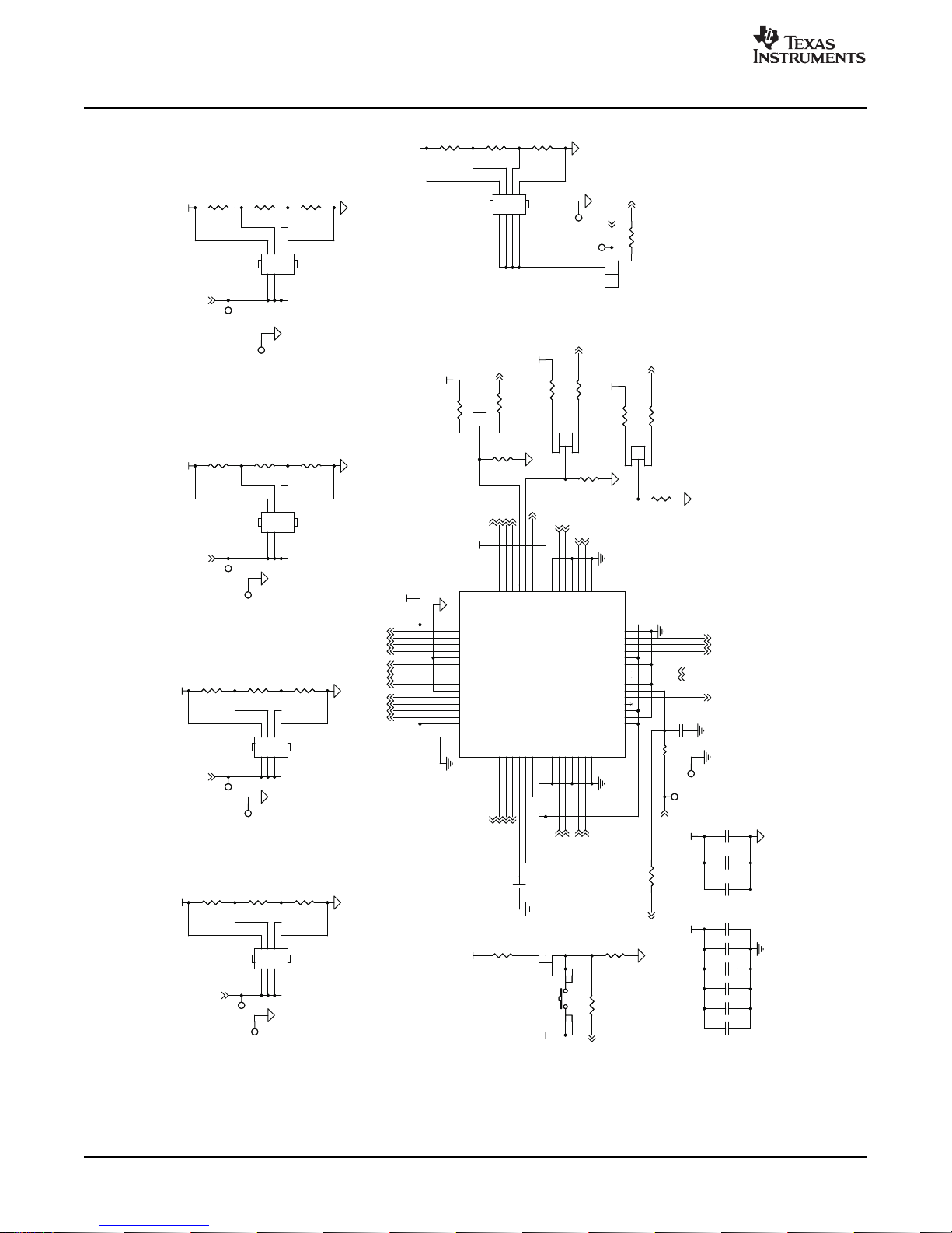
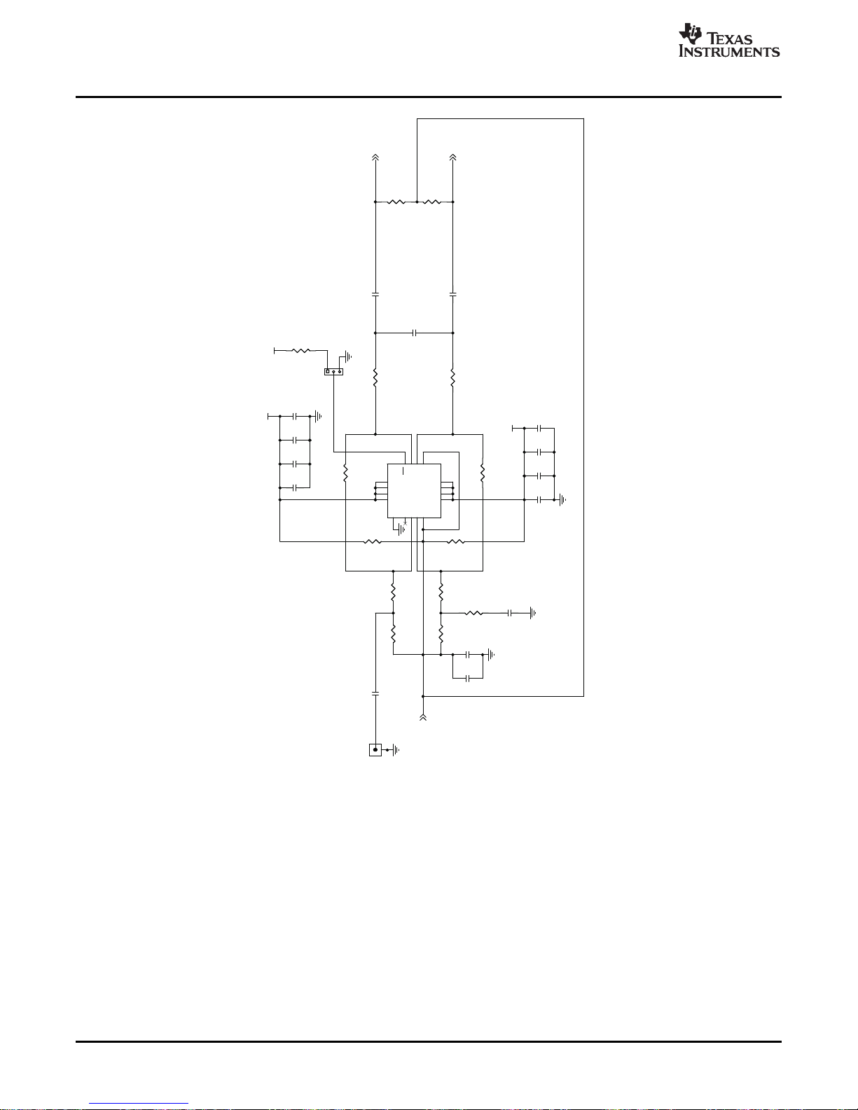
The schematic diagram for the EVM is in Section 4.3 .
2.2 ADC Circuit Function
The following sections describe the function of individual circuits. Refer to the relevant data sheet for
device operating characteristics.
2.2.1 ADC Operational Mode
By default, the ADC is configured to operate in parallel-mode operation, because the surface-mount
jumper asserts a 3.3-V state to the ADC reset pin. Consequenty, the SW1 reset pushbutton must be
pressed only when the device is configured into serial operational mode. Because the ADC is in parallel
operation mode, voltages are used to set the ADC modes. Users can use the EVM silkscreen to set the
operation modes.
2.2.2 ADC Power
Power is supplied to the EVM via banana jack sockets. Separate connections are provided for a 3.3-V
digital buffer supply (P1) and 3.3-V analog supply (P3). In most cases, these can be shorted together for
ADC evaluation. When using the amplifier evaluation path, users must connect the positive rail to J21 and
the negative rail to J22. The voltages depend on the coupling method and connection to the ADC. If the
ADC VCM is not supplied to the amplifier and the amplifier is connected to the ADC in a dc-coupled
fashion, users should set J21 to 4 V and J22 to –1 V. In ac-coupled configurations where the ADC VCM
biases the ADC inputs, users can connect J21 to 5 V and J22 to GND.
Circuit Description
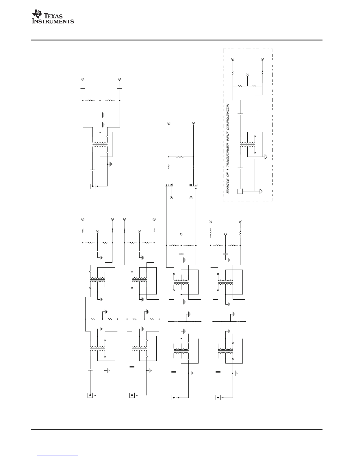
2.2.3 ADC Analog Inputs
The EVM is configured to accept a single-ended input souce and convert it to an ac-coupled differential
signal using a transformer. The inputs to the ADC must be dc-biased, which is accomplished by using the
ADC VCM output. The inputs are provided via SMA connectors J10 for ADC channel A, J11 for ADC
channel B, J13 for ADC channel C, and J14 for ADC channel D. ADC input channel C also includes the
option for ADC evaluation using an amplifier signal chain.
TI has tested this ADC with a variety of transformer brands, transorfmer configurations and terminations.
For many applications, a single low-cost transformer can be used in the input signal chain to a very high
degree of performance. Customers should select a transformer configuration based on their ADC input
bandwidth frequency. To assist in this process, TI has swept the analog input frequency and plotted the
resulting ADC SFDR performance with various transformers. Figure 1 and Figure 2 show the ADC
performance using the Mini-Circuits TC1-1T, Mini-Circuits TC4-1W, and Coilcraft WBC1-1TLB in one- and
two-tranformer configurations, respectively. In both plots, the results were taken on an ADS6443, sampling
at 80 MSPS and on the same input channel. The termination was changed according to the impedance
ratio of the transfomer used.
Using SMA input J2, users can evaluate the ADC using a THS4509 amplifier, which converts a
single-ended input into a differential signal while providing 10 dB of signal gain. Users should enable the
amplifier path by connecting JP6 1–2 and by shorting positions 1–2 on both surface-mount jumpers JP1
and JP2. At low input frequencies, the ADC represents a high input impedance and R10, R19, and C45
form a low-pass filter with a 3-db cutoff frequency of 70 MHz. Users should change these component
values depending on the bandwidth of the signal they are digitizing to band-limit the input noise into the
ADC. Using an excessively high cutoff frequency degrades the SNR of the system. Before users begin
evaluation of the amplifier path, one most choose whether to dc-couple or ac-couple to the amplifier path.
In a dc-coupled system, users should replace C46 and C47 with 0- Ω resistors and remove R9 and R18.
The ADC VCM should be used to set the CM input of the amplifier by making sure R84 is populated with a
0- Ω resistor. Because the ADC has a common-mode voltage of 1.5 V, and because the THS4509 is not a
rail-to-rail amplifier, users should adjust VCC to 4 V and –VCC to –1 V, which can be done by applying the
respective voltages to J21 and J22.
SLAU196 – April 2007 7
Submit Documentation Feedback
Page 8

www.ti.com
45
50
55
60
65
70
75
80
85
90
95
100
f − Frequency − MHz
SFDR − Spurious−Free Dynamic Range − dBc
G001
9.97 30.13 50.13 69.59 89.75 130.13 230.53 301.13 401.13 501.13
Mini Circuits
TC4−1W
Mini Circuits
TC1−1T
Coilcraft
WBC1−1TLB
45
50
55
60
65
70
75
80
85
90
95
100
f − Frequency − MHz
SFDR − Spurious−Free Dynamic Range − dBc
G002
9.97 30.13 50.13 69.59 89.75 130.13 230.53 301.13 401.13 501.13
Mini Circuits
TC4−1W
Mini Circuits
TC1−1T
Coilcraft
WBC1−1TLB
Circuit Description
For an ac-coupled system, users should use the voltage divider R9 and R18 to set the common-mode
input of the amplifier, which should be set to the midpoint of the amplifier supply. C46 and C47 ac-couple
the system, and the ADC inputs can then be biased by the R14 and R15 combination. Another ac-coupled
approach, not supported on this EVM, would be to use a transformer at the outputs of the THS4509. In
this case, the transformer would provide for ac-coupling, and one could bias the inputs of the ADC by
feeding the ADC VCM to the transformer center tap on the secondary.
It should be noted that the THS4509 used on this EVM is pinout-compatible with the THS4508, THS4511,
THS4513, and THS4520. Users can easily interchange the amplifier on this EVM and should pick the
appropriate amplifier based on commmon mode range, power supplies, and frequency of operation. TI
application engineers can assist in the best selection of these amplifiers based on the user requirements.
SFDR vs Frequency Using a Single Transformer
SFDR vs Frequency Using a Dual Transformer
8 SLAU196 – April 2007
Figure 1.
Figure 2.
Submit Documentation Feedback
Page 9

www.ti.com
2.2.4 ADC Clock Input
Users should connect a filtered, low-phase-noise clock input to J12. A transformer, T5, provides the
conversion from a single-ended clock signal into a differential clock signal. When selecting the clock signal
level, users should account for the transformer having an impedance ratio of 4, with a voltage step-up
of 2.
2.2.5 ADC Digital Outputs
The ADS64XX ADC outputs serialized data, a bit clock (DCLK), and a frame clock (FCLK). These signals
are brought to a high-density Samtec™ connector, J15. Users have three options in processing the ADC
data.
1. Customers can use the mating logic analyzer breakout board and capture the ADC data using a logic
analyzer. Users would be required to perform a software deserialization of the digital data before
conducting analysis. Contact the factory for a breakout board for your logic analyzer.
2. Customers can create their own digital interface card which directly interfaces to the ADC. In this case,
customers would design their mating digital interface board with the Samtec part number
QSH-060-01-F-D-A, which is the companion part number to the EVM connector.
3. In most cases, customers can use a hardware deserialization solution such as the TSW1200. The
TSW1200 features a powerful Xilinx™ Virtex 4 that comes preloaded with both 12-bit and 14-bit
deserialization routines. In addition, customers can use the FPGA to develop their own deserializer and
digital prototypes. The digital output of the TSW1200 easily plugs into logic analyzers or TI's own
digital capture and analysis solution, the TSW1100.
Circuit Description
2.2.6 Surface-Mount Jumper Selections
The EVM features surface-mount jumpers in cases where either the signal integrity is important or the
functions are not often used. Table 2 summarizes these options.
ADC Reference Designator Default Selection Optional Selection
Signal
RESET J7 2–3, parallel mode operation 1–2, serial mode
SCLK J6 Not populated, pin tied low 1–2, TSW1200 control
SDATA J8 Not populated, pin tied low 1–2, TSW1200 control
SEN J5 2–3: EVM J16 controls parallel operation modes 1–2, TSW1200 control
PD J9 Not populated, pin tied low, device operational 1–2, TSW1200 control
INC_M JP1 2–3, Transformer-coupled analog input to channel C 1–2, Amplifier-coupled
INC_P JP2 2–3, Transformer-coupled analog input to channel C 1–2, Amplifier-coupled
2.3 Deserialization and the TSW1200
While the specifics of the deserializer are out of the scope of this user's guide, TI has partnered up with
Xilinx to deliver an open-source deserializer solution with application note documentation. When designing
the deserializer, users should consult Xilinx application note XAPP866, hosted on the Xilinx website. In
addition, TI has provided a guide to understanding the different digital output modes of the ADC and how
to pick the most appropriate digital output mode for deserialization. Users should consult Demystifying the
Digital Output Choices of the ADS6XXX, TI application note SLAA348 .
Table 2. Surface Mount Jumpers
operation
over SCLK
over SDATA
over SEN
over PD
path to channel C
path to channel C
SLAU196 – April 2007 9
Submit Documentation Feedback
Page 10

www.ti.com
ADC Evaluation
3 ADC Evaluation
This chapter describes how to set up a typical ADC evaluation system that is similar to what TI uses to
perform testing for datasheet generation. Consequently, the information in this section is generic in nature
and is applicable to all high-speed, high-resolution ADC evaluations. This chapter covers signal tone
analysis, which yields ADC datasheet figures of merit such as signal-to-noise ratio (SNR) and spurious
free dynamic range (SFDR).
3.1 Hardware Selection
To reveal the true performance of the ADC under evaluation, tremendous care should be taken in
selecting both the ADC signal source and ADC clocking source. The hardware setup that TI uses for its
analysis is shown graphically in Figure 3 .
3.1.1 Analog Input Signal Generator
When choosing the quality of the ADC analog input source, one should consider both harmonic distortion
performance of the signal generator and the noise performance of the source.
In many cases, the harmonic distortion performance of the signal generator is inferior to that of the ADC,
and additional filtering is needed if users expect to reproduce the ADC SFDR numbers found in the data
sheet. Users can easily evaluate the harmonic distortion of their signal generator by hooking it directly to a
spectrum analyzer and measuring the power of the output signal and comparing that to the power of the
integer multiples of the output signal's frequency. If the harmonic distortion is worse then the ADC under
evaluation, the ADC digitizes the performance of the signal generator and the ADC's true SFDR is
masked. To alleviate this, it is recommended that users provide additional LC filtering after the signal
generator output.
Another important metric when deciding on a signal generator is its noise performance. As with the
distortion performance, if the noise performance is worse than that of the ADC under evaluation, the ADC
digitizes the performance of the source. Noise can be broken into two components, broadband noise and
close-in phase noise. Broadband noise can be improved by the LC filter added to improve distortion
performance; however, the close-in phase noise typically cannot be improved by additional filtering.
Therefore, when selecting an analog signal source it is extremely important to review the manufacturer's
phase noise plots, and great care should be taken to choose a signal generator with the best phase-noise
performance.
3.1.2 Clock Signal Generator
Equally important in the high-performance ADC evaluation setup is the selection of the clocking source.
Most modern ADCs, the ADS64XX included, accept either a sinusoidal or a square-wave clock input. The
key metric in selecting a clocking source is selecting a source with the lowest jitter. This becomes
increasingly important as the ADC's input frequency (Fin) increases, because the ADC SNR evaluation
setups can become jitter-limited (Tj) as shown by the following equation.
SNR (dBc) = 20 log (2 π × Fin × Tj(rms))
In theory, a square-wave source with femtosecond jitter would be ideal for an ADC evaluation setup.
However, in practical terms, most commercially available square-wave generators offer jitter measured in
picoseconds, which is too great for high-resolution ADC evaluation setups. Therefore, most evaluation
setups rely on the ADC's internal clock buffer to convert a sinusoidal input signal into a ultralow-jitter
square wave. When selecting a sinusoidal clocking source, it has been shown that phase noise has a
direct impact on jitter performance. Consequently, great scrutiny should be applied to the phase-noise
performance of the clocking signal generator. TI has found that high-Q monolithic crystal filters can
improve the phase noise of the signal generator, and they become essential elements of the evaluation
setup when high ADC input frequencies are being evaluated.
10 SLAU196 – April 2007
Submit Documentation Feedback
Page 11

www.ti.com
3.2 Coherent Input Frequency Selection
Typical ADC analysis requires users to collect the resulting time-domain data and perform a Fourier
transform to analyze the data in the frequency domain. A stipulation of the Fourier transform is that the
signal must be continuous-time; however, this is not practical when looking at a finite set of ADC samples,
usually collected from a logic analyzer. Consequently, users typically apply a window function to minimize
the time-domain discontinuities that arise when analyzing a finite set of samples. For ADC analysis,
window functions have their own frequency signatures or lobes that distort both SNR and SFDR
measurements fo the ADC.
TI uses the concept of coherent sampling to work around the use of a window function. The central
premise of coherent sampling entails that the input signal into the ADC is carefully chosen such that when
a continuous-time signal is reconstructed from a finite sample set; no time-domain discontinuities exist. To
achieve this, the input frequency must be an integer multiple of the ratio of the ADC's sample rate (fs) and
the number of samples collected from the logic analyzer (N
the fundamental frequency (ff). Determining the ADC input frequency is a two-step process. First, the
users select the frequency of interest for evaluating the ADC; then they divide this by the fundamental
frequency. This typically yields a non-integer value, which should be rounded to the nearest odd,
preferably prime, integer. Once that integer, or frequency bin (f
this with the fundamental frequency to obtain a coherent frequency to program into their ADC input signal
generator. The procedure is summarized as follows.
ff= fs/N
f
Coherent frequency = ff× f
s
= Odd_round(f
bin
ADC Evaluation
). The ratio of fsto N
s
), has been determined, users multiply
bin
/ff)
desired
bin
is typically referred to as
s
SLAU196 – April 2007 11
Submit Documentation Feedback
Page 12

www.ti.com
ADC Evaluation
12 SLAU196 – April 2007
Figure 3. ADS64XX EVM Setup
Submit Documentation Feedback
Page 13

www.ti.com
4 Physical Description
K001
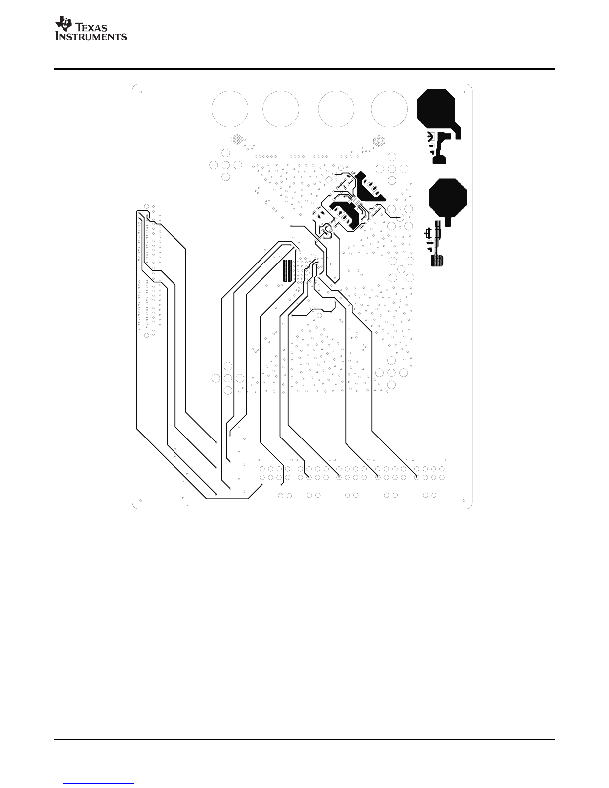
4.1 PCB Layout
Physical Description
This chapter describes the physical characteristics and PCB layout of the EVM.
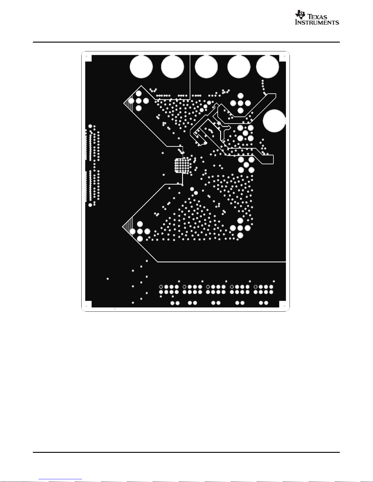
The EVM comprises six layers and is 62 mils thick. The EVM features a split ground plane, which can be
shorted together under the ADC by using the two exposed gold-plated strips seen in Figure 8 to make a
low-impedance connection between ground planes. By default, the ground planes are not connected
together and should be connected at the power supply. Although this board uses separate ground planes
between analog and digital supplies, it should be noted that TI has conducted experiments with both
single and split ground planes and found the performance to be identical. The ADC features a
constant-current LVDS output, which minimizes the coupling of digital output switching noise back to the
analog inputs.
SLAU196 – April 2007 13
Submit Documentation Feedback
Figure 4. Layer 1, Top Silkscreen
Page 14

www.ti.com
K002
Physical Description
14 SLAU196 – April 2007
Figure 5. Layer 2, Top Side
Submit Documentation Feedback
Page 15

www.ti.com
K003
Physical Description
SLAU196 – April 2007 15
Submit Documentation Feedback
Figure 6. Layer 3, Gound Plane
Page 16
www.ti.com
K004
Physical Description
16 SLAU196 – April 2007
Figure 7. Layer 4, Power Plane
Submit Documentation Feedback
Page 17
www.ti.com
K005
Physical Description
SLAU196 – April 2007 17
Submit Documentation Feedback
Figure 8. Layer 5, Bottom Side
Page 18

www.ti.com
K006
Physical Description
18 SLAU196 – April 2007
Figure 9. Layer 6, Bottom Silkscreen
Submit Documentation Feedback
Page 19

www.ti.com
4.2 Bill of Materials
Physical Description
Table 3 is the bill of materials for the ADS64XXEVM.
Table 3. ADS64XXEVM Bill of Materials
Reference Quantity Part Part Number Manufacturer
C1, C5, C8, C10 4 22 µ F ECS-T1CC226R Panasonic
C2, C9 2 10 µ F ECS-H1CC106R Panasonic
C3, C6 2 1 µ F ECJ-1VB1A105K Panasonic
C4, C7, C12, C13, C14, C15,
C16, C17, C18, C19, C20,
C21, C22, C23, C24, C25, 24 0.1 µ F GRM188R71H104KA93D Murata
C26, C27, C28, C29, C30,
C31, C32, C33
C11 1 2000 pF GRM1885C1H202JA01D Murata
C34, C37, C40, C42, C56,
C57
C35, C36, C38, C39, C41,
C43, C46, C47 C48, C53, 11 0.1 µ F ECJ-1VB1C104K Panasonic
C55
C44 1 0.22 µ F ECJ-1VB1A224K Panasonic
C45 1 18 pF ECJ-1VC1H180J Panasonic
C52, C54 2 33 µ F TPSB336K016R0350 EPCOS Inc.
D1, D2 2 Green LNJ312G8TRA Panasonic
J2, J10, J11, J12, J13, J14 6 SMA 142-0701-201 Johnson Components
J5, J7 2 SMD3P_BRIDGE
J6, J8, J9 3 SMD3P_BRIDGE No part Leave as is
J15 1 CONN_QTH_30X2-D-A QTH-60-02-F-D-A
J16, J17, J18, J19, J20 5 Header 4x2 90131-0124 Molex
JP1, JP2 2 Jumper_1x3_SMT No part
JP6 1 Jumper_1x3 929400-01-36 3M
L1, L2 2 Bead, 220– Ω EXC-3BB221H Panasonic
L8, L9 2 68 EXC-ML32A680U Panasonic
MP2 4 PMS 440 0038 PH Building Fasteners
MP3 4 1902C Keystone Electronic
P1, P3, J21, J22 4 Banana jack, red 845R SPC Technology
P2, P4 2 Banana jack, black 845B SPC Technology
R1, R2 2 750 Ω ERJ-3EKF7500V Panasonic
R8, R22 2 348 Ω ERJ-3EKF3480V Panasonic
R9, R18 2 499 Ω ERJ-3EKF4990V Panasonic
R10, R19, R21, R48, R49,
R54, R56, R62, R63, R68, 11 49.9 Ω ERJ-3EKF49R9V Panasonic
R69
R13, R16 2 69.8 Ω ERJ-3EKF69R8V Panasonic
R12, R17, R31, R35, R37,
R38, R39, R42, R43, R55, 11 100 Ω ERJ-3EKF1000V Panasonic
R59
R14, R15, R20 0 200 Ω ERJ-3EKF2000V Panasonic
6 10 µ F ECJ-2FB1A106K Panasonic
Not
Installed
Short pins 2 and 3
using 0 Ω
Short pins 2 and 3
using 0 Ω
Screw machine, PH 4-40
× 3/8
Stand-off hex
.5/4-40THR
Not
installed
SLAU196 – April 2007 19
Submit Documentation Feedback
Page 20

www.ti.com
Physical Description
Table 3. ADS64XXEVM Bill of Materials (continued)
Reference Quantity Part Part Number Manufacturer
R28, R29, R32, R36, R72,
R73, R74, R75, R76, R77, 15 1 k Ω ERJ-3EKF1001V Panasonic
R78, R79, R80, R81, R82
R30, R84 2 0 Ω ERJ-3GEY0R00V Panasonic
R33, R34, R40, R41, R44,
R83
R45, R46, R51, R52, R58,
R60, R65, R66, R71
R47, R50, R53, R57, R61,
R64, R67, R70
SW1 1 Switch, pushbutton KT11P3JM C & K Switch
T1, T2, T3, T4, T5, T6, T7,
T8, T9
TP1, TP2, TP3, TP4, TP9,
TP12
TP5, TP6, TP7, TP8, TP10,
TP11
U1 1 ADS64XX
U2 1 THS4509 THS4509RGTT TI
6 10 k Ω ERJ-3EKF1002V Panasonic
9 10 Ω ERJ-3EKF10R0V Panasonic
8 200 Ω ERJ-3EKF2000V Panasonic
9 WBC1-1TLB WBC1-1TLB Coilcraft
6 Test point, black 5001 Keystone
6 Test point, white 5002 Keystone
5 Conn. jumper, shorting S9000-ND Digi-Key
Not
Installed
20 SLAU196 – April 2007
Submit Documentation Feedback
Page 21
www.ti.com
PWR_IN1
PWR_IN2
+5V_IN
-5V_IN
+3.3VA
+3.3VD
+5V_AMP
-5V_AMP
+
C54
33UF
16V
+
C54
33UF
16V
12
+
C8
22uF
+
C8
22uF
12
+
C2
10uF
+
C2
10uF
12
P1
Bananajackred
P1
Bananajackred
1
1
C57
10uF
10V
C57
10uF
10V
12
C55
.1uF
16V
C55
.1uF
16V
L2
Bead220ohm
L2
Bead220ohm
1
2
+
C1
22uF
+
C1
22uF
12
+
C10
22uF
+
C10
22uF
12
P2
Bananajackblack
P2
Bananajackblack
1
1
L968L9
68
1
2
L868L8
68
1
2
C7
.1uFC7.1uF
12
P3
Bananajackred
P3
Bananajackred
1
1
+
C5
22uF
+
C5
22uF
12
C6
1uFC61uF
12
+
C52
33UF
16V
+
C52
33UF
16V
12
P4
Bananajackblack
P4
Bananajackblack
1
1
D1
GREEND1GREEN
12
J21
Bananajackred
+5V_AMP
J21
Bananajackred
+5V_AMP
L1
Bead220ohm
L1
Bead220ohm
1
2
C4
.1uFC4.1uF
12
+
C9
10uF
+
C9
10uF
12
C53
.1uF
16V
C53
.1uF
16V
D2
GREEND2GREEN
12
R1
750R1750
12
C56
10uF
10V
C56
10uF
10V
1 2
C3
1uFC31uF
12
J22
Bananajackred
-5V_AMP
J22
Bananajackred
-5V_AMP
R2
750R2750
12
S001
Physical Description
4.3 PCB Schematics
Figure 10. Sheet 1 of 5
SLAU196 – April 2007 21
Submit Documentation Feedback
Page 22
www.ti.com
ICLKP
ICLKM
CAP
SCLK
SDA
TA
RESET
PDN
+3.3V
A
+3.3VD
+3.3VA
+3.3VD
+3.3VD
+3.3VD
+3.3VD
+3.3VD
+3.3VD
+3.3VA
+3.3VD
+3.3VD
+3.3VD
+3.3VD
+3.3VD
INA_M
INA_P
INB_M
INB_P
IND_M
IND_P
INC_M
INC_P
ICLKP
ICLKM
CM
DA1_P
DA1_M
DA0_P
DA0_M
DD0_M
DD1_P
DD1_M
DD0_P
DC1_P
DC1_M
DC0_P
DC0_M
DB1_P
DB1_M
DB0_P
DB0_M
DCLK_M
DCLK_P
FCLK_M
FCLK_P
CFG4
CFG3
CFG2
CFG1
FPGA_SDATA
FPGA_PDN
FPGA_SCLK
CFG1
CFG2
CFG3
CFG4
SEN
SEN
FPGA_SEN
FPGA_RST
AMP_VCM
PARALLELINTERFACE
SERIALINTERFACE
R791KR79
1K
12
R281KR28
1K
12
R811KR81
1K
12
R30
0OHM
R30
0OHM
R35 100R35 100
1
2
J5J5
123
R42 100R42 100
1
2
R291KR29
1K
12
R821KR82
1K
12
C11
2000pF
C11
2000pF
1
2
R45 10R45 10
R44
10K
R44
10K
12
TP7TP7
J17J17
246
8
135
7
TP9TP9
J6J6
123
R43 100R43 100
1
2
R361KR36
1K
12
R40
10K
R40
10K
12
C19
.1uF
C19
.1uF
12
U1
ADS64XXU1ADS64XX
DA1_P1DA1_M2DA0_P3DA0_M4CAP5RESET6LVDD7AGND8AVDD9AGND10INA_M11INA_P12AGND13INB_M14INB_P15AGND
16
AVDD
17
AGND
18
AVDD
19
NC
20
CFG4
21
CM
22
AGND
23
CLKP
24
CLKM
25
AGND
26
AVDD
27
CFG3
28
CFG2
29
CFG1
30
AGND
31
AVDD
32
AGND
33
INC_P
34
INC_M
35
AGND
36
IND_P
37
IND_M
38
AGND
39
AVDD
40
PDN
41
SEN
42
SDATA
43
SCLK
44
DD1_P
45
DD1_M
46
DD0_P
47
DD0_M
48
LVDD
49
DC1_P
50
DC1_M
51
DC0_P
52
DC0_M
53
LGND
54
FCLK_P
55
FCLK_M
56
DCLK_P
57
DCLK_M
58
LGND
59
DB1_P
60
DB1_M
61
DB0_P
62
DB0_M
63
LVDD
64
GND
65
TP4TP4
TP2TP2
R321KR32
1K
12
J18J18
246
8
135
7
J7J7
123
J9J9
123
SW1SW1
C21
.1uF
C21
.1uF
12
C20
.1uF
C20
.1uF
12
J19J19
246
8
135
7
TP11TP11
TP6TP6
TP1TP1
R721KR72
1K
12
TP10TP10
R38 100R38 100
1
2
J20J20
246
8
135
7
R34
10K
R34
10K
12
TP12TP12
R741KR74
1K
12
R771KR77
1K
12
R37 100R37 100
1
2
R39
100
R39
100
1
2
C18
.1uF
C18
.1uF
12
J8J8
123
C17
.1uF
C17
.1uF
12
R731KR73
1K
12
J16J16
246
8
135
7
R33
10K
R33
10K
12
TP3TP3
C16
.1uF
C16
.1uF
12
C12
.1uF
C12
.1uF
12
C15
.1uF
C15
.1uF
12
C14
.1uF
C14
.1uF
12
R751KR75
1K
12
TP8TP8
C13
.1uF
C13
.1uF
12
R781KR78
1K
12
R801KR80
1K
12
TP5TP5
R31 100R31 100
1
2
R41
10K
R41
10K
12
R84
ZERO
5%
1/8W
R84
ZERO
5%
1/8W
R761KR76
1K
12
S002
Physical Description
22 SLAU196 – April 2007
Figure 11. Sheet 2 of 5
Submit Documentation Feedback
Page 23
www.ti.com
SIGNAL_INA
SIGNAL_INB
SIGNAL_INC
SIGNAL_IND
INA_P
INA_M
CM
ICLKP
ICLKM
INB_P
INB_M
CM
CM
CM
INC_P
INC_M
IND_P
IND_M
AMP+
AMP-
CM
IN_P
IN_M
DoNotInstall
.1uF
1:1
1:1 1:1
1:1
1:1
1:1
1:1 1:1
.1uF
.1uF
EXAMPLEOF1TRANSFORMERINPUTCONFIGURATION
49.9
49.9
10
10
SMA
C22
.1uF
C22
.1uF
1
2
R46 10R46 10
R64
49.9
R64
49.9
C31
.1uF
C31
.1uF
1
2
R56
49.9
R56
49.9
T2
WBC1-1TLBT2WBC1-1TLB
3
2
1
6
5
4
R20
200
R20
200
C32
.1uF
C32
.1uF
1
2
MS
A
DEN
J10
SMA
MS
A
DEN
J10
SMA
1
5234
R70
49.9
R70
49.9
R61
49.9
R61
49.9
C25
.1uF
C25
.1uF
1
2
R55
100
R55
100
R54
49.9
R54
49.9
T1
WBC1-1TLBT1WBC1-1TLB
3
2
1
6
5
4
MS
A
DEN
J12
SMA
MS
A
DEN
J12
SMA
1
5234
T7
WBC1-1TLBT7WBC1-1TLB
3
2
1
6
5
4
R67
49.9
R67
49.9
R63
49.9
R63
49.9
T9
WBC1-1TLBT9WBC1-1TLB
3
2
1
6
5
4
R62
49.9
R62
49.9
R58 10R58 10
R69
49.9
R69
49.9
R48
49.9
R48
49.9
R68
49.9
R68
49.9
R52 10R52 10
C27
.1uF
C27
.1uF
1
2
R65 10R65 10
R49
49.9
R49
49.9
C29
.1uF
C29
.1uF
1
2
C26
.1uF
C26
.1uF
1
2
R71 10R71 10
1:11:1
3
2
1
6
5
4
T3
WBC1-1TLBT3WBC1-1TLB
3
2
1
6
5
4
R6010R60
10
C30
.1uF
C30
.1uF
1
2
R47
49.9
R47
49.9
R66 10R66 10
T6
WBC1-1TLBT6WBC1-1TLB
3
2
1
6
5
4
T8
WBC1-1TLBT8WBC1-1TLB
3
2
1
6
5
4
R5110R51
10
MS
A
DEN
J11
SMA
MS
A
DEN
J11
SMA
1
5234
JP2JP2
1
3
2
C33
.1uF
C33
.1uF
1
2
JP1JP1
1
3
2
C28
.1uF
C28
.1uF
1
2
C23
.1uF
C23
.1uF
1
2
MS A
DEN
J13
SMA
MS A
DEN
J13
SMA
1
5234
C24
.1uF
C24
.1uF
1
2
MS A
DEN
J14
SMA
MS A
DEN
J14
SMA
1
5234
R57
49.9
R57
49.9
R53
49.9
R53
49.9
T5
TC4-1WT5TC4-1W
3
2
1
6
5
4
R50
49.9
R50
49.9
R59
100
R59
100
T4
WBC1-1TLBT4WBC1-1TLB
3
2
1
6
5
4
S003
Physical Description
SLAU196 – April 2007 23
Submit Documentation Feedback
Figure 12. Sheet 3 of 5
Page 24
www.ti.com
PD
AMP_VCM
+5V_AMP
-5V_AMP
+5V_AMP
AMP_VCM
AMP+
AMP-
Default:Short2-3
DoNotInstall
DoNotInstall
MS A
DEN
J2
AMP
MS A
DEN
J2
AMP
1
5234
C40
10uF
10V
C40
10uF
10V
12
C37
10uF
10V
C37
10uF
10V
12
R14
200
R14
200
R19
49.9
R19
49.9
R21
49.9
R21
49.9
R18
499
R18
499
C41
.1uF
16V
C41
.1uF
16V
C46
.1uF
C46
.1uF
C48
.1uF
16V
C48
.1uF
16V
C38
.1uF
16V
C38
.1uF
16V
C42
10uF
10V
C42
10uF
10V
12
C34
10uF
10V
C34
10uF
10V
12
JP6JP6
1
3
2
R15
200
R15
200
R16
69.8
R16
69.8
R10
49.9
R10
49.9
C43
.1uF
16V
C43
.1uF
16V
C35
.1uF
16V
C35
.1uF
16V
R17
100
R17
100
R83
10K
1/10W
1%
R83
10K
1/10W
1%
R22
348
R22
348
R12
100
R12
100
R8
348R8348
C44
.22uF
C44
.22uF
R9
499R9499
U2
THS4509U2THS4509
NC1VIN-2CM1
4
VS+
5
VS+
6
VOUT+3VS+
7
VS+
8
CM2
9
VOUT
-
10
VIN+
11
PD
12
VS-
13
VS-
14
VS-
15
VS-
16
P
AD
17
C39
.1uF
16V
C39
.1uF
16V
C36
.1uF
16V
C36
.1uF
16V
C45
18pF
C45
18pF
C47
.1uF
C47
.1uF
R13
69.8
R13
69.8
S004
Physical Description
24 SLAU196 – April 2007
Figure 13. Sheet 4 of 5
Submit Documentation Feedback
Page 25
www.ti.com
DA0_M
DA0_P
DA1_M
DA1_P
DB0_M
DB0_P
DB1_M
DB1_P
DCLK_M
DCLK_P
FCLK_M
FCLK_P
DC0_M
DC0_P
DC1_M
DC1_P
DD0_M
DD0_P
DD1_M
DD1_P
FPGA_PDN
FPGA_SCLK
FPGA_SDA
TA
FPGA_SEN
FPGA_RST
J15
CONN_QTH_30X2-D-A
J15
CONN_QTH_30X2-D-A
246
8
101214161820222426283032343638
40
135791113151719212325272931333537
39
G1G2G3G4G5G6G7
G8
4142434445464748495051525354555657585960616263646566676869707172737475767778798081828384858687888990919293949596979899
100
101
102
103
104
105
106
107
108
109
110
111
112
113
114
115
116
117
118
119
120
S005
Figure 14. Sheet 5 of 5
Physical Description
SLAU196 – April 2007 25
Submit Documentation Feedback
Page 26

EVALUATION BOARD/KIT IMPORTANT NOTICE
Texas Instruments (TI) provides the enclosed product(s) under the following conditions:
This evaluation board/kit is intended for use for ENGINEERING DEVELOPMENT, DEMONSTRATION, OR EVALUATION PURPOSES
ONLY and is not considered by TI to be a finished end-product fit for general consumer use. Persons handling the product(s) must have
electronics training and observe good engineering practice standards. As such, the goods being provided are not intended to be complete
in terms of required design-, marketing-, and/or manufacturing-related protective considerations, including product safety and environmental
measures typically found in end products that incorporate such semiconductor components or circuit boards. This evaluation board/kit does
not fall within the scope of the European Union directives regarding electromagnetic compatibility, restricted substances (RoHS), recycling
(WEEE), FCC, CE or UL, and therefore may not meet the technical requirements of these directives or other related directives.
Should this evaluation board/kit not meet the specifications indicated in the User’s Guide, the board/kit may be returned within 30 days from
the date of delivery for a full refund. THE FOREGOING WARRANTY IS THE EXCLUSIVE WARRANTY MADE BY SELLER TO BUYER
AND IS IN LIEU OF ALL OTHER WARRANTIES, EXPRESSED, IMPLIED, OR STATUTORY, INCLUDING ANY WARRANTY OF
MERCHANTABILITY OR FITNESS FOR ANY PARTICULAR PURPOSE.
The user assumes all responsibility and liability for proper and safe handling of the goods. Further, the user indemnifies TI from all claims
arising from the handling or use of the goods. Due to the open construction of the product, it is the user’s responsibility to take any and all
appropriate precautions with regard to electrostatic discharge.
EXCEPT TO THE EXTENT OF THE INDEMNITY SET FORTH ABOVE, NEITHER PARTY SHALL BE LIABLE TO THE OTHER FOR ANY
INDIRECT, SPECIAL, INCIDENTAL, OR CONSEQUENTIAL DAMAGES.
TI currently deals with a variety of customers for products, and therefore our arrangement with the user is not exclusive.
TI assumes no liability for applications assistance, customer product design, software performance, or infringement of patents or
services described herein.
Please read the User’s Guide and, specifically, the Warnings and Restrictions notice in the User’s Guide prior to handling the product. This
notice contains important safety information about temperatures and voltages. For additional information on TI’s environmental and/or
safety programs, please contact the TI application engineer or visit www.ti.com/esh .
No license is granted under any patent right or other intellectual property right of TI covering or relating to any machine, process, or
combination in which such TI products or services might be or are used.
FCC Warning
This evaluation board/kit is intended for use for ENGINEERING DEVELOPMENT, DEMONSTRATION, OR EVALUATION PURPOSES
ONLY and is not considered by TI to be a finished end-product fit for general consumer use. It generates, uses, and can radiate radio
frequency energy and has not been tested for compliance with the limits of computing devices pursuant to part 15 of FCC rules, which are
designed to provide reasonable protection against radio frequency interference. Operation of this equipment in other environments may
cause interference with radio communications, in which case the user at his own expense will be required to take whatever measures may
be required to correct this interference.
EVM WARNINGS AND RESTRICTIONS
It is important to operate this EVM within the input voltage range of –0.3 V to 3.8 V and the output voltage range of –0.3 V to 3.8 V.
Exceeding the specified input range may cause unexpected operation and/or irreversible damage to the EVM. If there are questions
concerning the input range, please contact a TI field representative prior to connecting the input power.
Applying loads outside of the specified output range may result in unintended operation and/or possible permanent damage to the EVM.
Please consult the EVM User's Guide prior to connecting any load to the EVM output. If there is uncertainty as to the load specification,
please contact a TI field representative.
During normal operation, some circuit components may have case temperatures greater than 25 ° C. The EVM is designed to operate
properly with certain components above 50 ° C as long as the input and output ranges are maintained. These components include but are
not limited to linear regulators, switching transistors, pass transistors, and current sense resistors. These types of devices can be identified
using the EVM schematic located in the EVM User's Guide. When placing measurement probes near these devices during operation,
please be aware that these devices may be very warm to the touch.
Mailing Address: Texas Instruments, Post Office Box 655303, Dallas, Texas 75265
Copyright 2008, Texas Instruments Incorporated
Page 27

IMPORTANT NOTICE
Texas Instruments Incorporated and its subsidiaries (TI) reserve the right to make corrections, modifications, enhancements, improvements,
and other changes to its products and services at any time and to discontinue any product or service without notice. Customers should
obtain the latest relevant information before placing orders and should verify that such information is current and complete. All products are
sold subject to TI’s terms and conditions of sale supplied at the time of order acknowledgment.
TI warrants performance of its hardware products to the specifications applicable at the time of sale in accordance with TI’s standard
warranty. Testing and other quality control techniques are used to the extent TI deems necessary to support this warranty. Except where
mandated by government requirements, testing of all parameters of each product is not necessarily performed.
TI assumes no liability for applications assistance or customer product design. Customers are responsible for their products and
applications using TI components. To minimize the risks associated with customer products and applications, customers should provide
adequate design and operating safeguards.
TI does not warrant or represent that any license, either express or implied, is granted under any TI patent right, copyright, mask work right,
or other TI intellectual property right relating to any combination, machine, or process in which TI products or services are used. Information
published by TI regarding third-party products or services does not constitute a license from TI to use such products or services or a
warranty or endorsement thereof. Use of such information may require a license from a third party under the patents or other intellectual
property of the third party, or a license from TI under the patents or other intellectual property of TI.
Reproduction of TI information in TI data books or data sheets is permissible only if reproduction is without alteration and is accompanied
by all associated warranties, conditions, limitations, and notices. Reproduction of this information with alteration is an unfair and deceptive
business practice. TI is not responsible or liable for such altered documentation. Information of third parties may be subject to additional
restrictions.
Resale of TI products or services with statements different from or beyond the parameters stated by TI for that product or service voids all
express and any implied warranties for the associated TI product or service and is an unfair and deceptive business practice. TI is not
responsible or liable for any such statements.
TI products are not authorized for use in safety-critical applications (such as life support) where a failure of the TI product would reasonably
be expected to cause severe personal injury or death, unless officers of the parties have executed an agreement specifically governing
such use. Buyers represent that they have all necessary expertise in the safety and regulatory ramifications of their applications, and
acknowledge and agree that they are solely responsible for all legal, regulatory and safety-related requirements concerning their products
and any use of TI products in such safety-critical applications, notwithstanding any applications-related information or support that may be
provided by TI. Further, Buyers must fully indemnify TI and its representatives against any damages arising out of the use of TI products in
such safety-critical applications.
TI products are neither designed nor intended for use in military/aerospace applications or environments unless the TI products are
specifically designated by TI as military-grade or "enhanced plastic." Only products designated by TI as military-grade meet military
specifications. Buyers acknowledge and agree that any such use of TI products which TI has not designated as military-grade is solely at
the Buyer's risk, and that they are solely responsible for compliance with all legal and regulatory requirements in connection with such use.
TI products are neither designed nor intended for use in automotive applications or environments unless the specific TI products are
designated by TI as compliant with ISO/TS 16949 requirements. Buyers acknowledge and agree that, if they use any non-designated
products in automotive applications, TI will not be responsible for any failure to meet such requirements.
Following are URLs where you can obtain information on other Texas Instruments products and application solutions:
Products Applications
Amplifiers amplifier.ti.com Audio www.ti.com/audio
Data Converters dataconverter.ti.com Automotive www.ti.com/automotive
DSP dsp.ti.com Broadband www.ti.com/broadband
Clocks and Timers www.ti.com/clocks Digital Control www.ti.com/digitalcontrol
Interface interface.ti.com Medical www.ti.com/medical
Logic logic.ti.com Military www.ti.com/military
Power Mgmt power.ti.com Optical Networking www.ti.com/opticalnetwork
Microcontrollers microcontroller.ti.com Security www.ti.com/security
RFID www.ti-rfid.com Telephony www.ti.com/telephony
RF/IF and ZigBee® Solutions www.ti.com/lprf Video & Imaging www.ti.com/video
Mailing Address: Texas Instruments, Post Office Box 655303, Dallas, Texas 75265
Copyright 2008, Texas Instruments Incorporated
Wireless www.ti.com/wireless
Page 28

Mouser Electronics
Authorized Distributor
Click to View Pricing, Inventory, Delivery & Lifecycle Information:
Texas Instruments:
ADS6423EVM ADS6443EVM
 Loading...