

Page 1

ADS61xx and ADS61B23EVM
User's Guide
Literature Number: SLAU206B
September 2007 – Revised April 2008
Page 2

2 SLAU206B – September 2007 – Revised April 2008
Submit Documentation Feedback
Page 3

Contents
1 Overview ............................................................................................................................. 5
1.1 ADS61xx/ADS61B23 EVM Quick-Start Procedure ................................................................... 5
2 Circuit Description ............................................................................................................... 6
2.1 Schematic Diagram ....................................................................................................... 6
2.2 ADC Circuit Function ..................................................................................................... 6
3 TI ADC SPI Control Interface ................................................................................................ 10
3.1 Installing the ADC SPI Control Software ............................................................................. 10
3.2 Setting Up the EVM for ADC SPI Control ............................................................................ 11
3.3 Using the TI ADC SPI Interface Software ............................................................................ 11
4 Connecting to FPGA Platforms ............................................................................................ 13
4.1 TSW1100 ................................................................................................................. 13
4.2 TSW1200 ................................................................................................................. 13
5 ADC Evaluation .................................................................................................................. 14
5.1 Hardware Selection ..................................................................................................... 14
5.2 Coherent Input Frequency Selection .................................................................................. 15
6 Physical Description ........................................................................................................... 16
6.1 PCB Layout ............................................................................................................... 16
6.2 Bill of Materials ........................................................................................................... 21
6.3 EVM Schematics ........................................................................................................ 23
Important Notices ............................................................................................................... 29
SLAU206B – September 2007 – Revised April 2008 Table of Contents 3
Submit Documentation Feedback
Page 4

www.ti.com
List of Figures
1 TI ADC SPC Interface Screen ........................................................................................... 10
2 Top Silkscreen .............................................................................................................. 16
3 Component Side ............................................................................................................ 17
4 Ground Plane 1 ............................................................................................................. 18
5 Power Plane 1 .............................................................................................................. 19
6 Bottom Side ................................................................................................................. 20
7 EVM Schematic, Sheet 1 .................................................................................................. 23
8 EVM Schematic, Sheet 2 .................................................................................................. 24
9 EVM Schematic, Sheet 3 .................................................................................................. 25
10 EVM Schematic, Sheet 4 .................................................................................................. 26
11 EVM Schematic, Sheet 5 .................................................................................................. 27
12 Breakout Board Schematic, Sheet 6 ..................................................................................... 28
List of Tables
1 Breakout Board Pin Assignments.......................................................................................... 8
2 Jumpers ....................................................................................................................... 9
3 Surface-Mount Jumpers .................................................................................................... 9
4 ADS61xx Frequently Used Registers .................................................................................... 12
5 Bill of Materials ............................................................................................................. 21
4 List of Figures SLAU206B – September 2007 – Revised April 2008
Submit Documentation Feedback
Page 5

1 Overview
This user's guide gives a general overview of the evaluation module (EVM) and provides a general
description of the features and functions to be considered while using this module. This manual is
applicable to the ADS6122, ADS6123, ADS6124, ADS6125, ADS6142, ADS6143, ADS6144, ADS6145,
and ADS61B23, which collectively are referred to as ADS61xx and ADS61B23. The ADS61xx/ADS61B23
EVM provides a platform for evaluating the low-power, single-channel ADS61xx/ADS61B23 12- and 14-bit
analog-to-digital converters (ADC), and the ADS61B23 12-bit ADC with buffered analog input under
various signal, reference, and supply conditions.
This document should be used in combination with the respective ADC data sheet.
1.1 ADS61xx/ADS61B23 EVM Quick-Start Procedure
Using the quick-start procedure, many users can begin evaluating the ADC in a short time. The quick-start
procedure uses the default conditions of the EVM as shipped from the factory. In addition, the quick-start
guide configures the ADC in a CMOS offset binary data format. Users who have modified the board may
find the quick-start procedure to be ineffective.
1. Supply 3.3 V to J11 while connecting the return to a shorted J11 and J14. Power on the device.
2. Confirm jumper J6 is shorted 1–2 and jumpers J2, J3, and J7 have positions 2–3 shorted.
3. Use the silkscreen to confirm jumper J1 is set to Offset Binary, CMOS output.
4. Use the silkscreen to confirm jumper J4 is set to 0dB Gain, Int Ref.
5. Supply a –1-dBFS filtered, low-phase-noise, 10-MHz CW tone into J8.
6. Supply a filtered, low-phase-noise clock to J9.
7. Use the accompanying breakout board and monitor the digital output (see Table 1 ).
User's Guide
SLAU206B – September 2007 – Revised April 2008
Windows is a registered trademark of Microsoft Corporation.
Samtec is a trademark of Samtec, Inc.
Xilinx, Virtex are trademarks of Xilinx, Inc.
All other trademarks are the property of their respective owners.
SLAU206B – September 2007 – Revised April 2008 5
Submit Documentation Feedback
Page 6

Circuit Description
2 Circuit Description
2.1 Schematic Diagram
The schematic diagram for the EVM is in Section 6.3 .
2.2 ADC Circuit Function
The following sections describe the function of individual circuits. See the relevant data sheet for device
operating characteristics.
2.2.1 ADC Operational Mode
By default, the ADC is configured to operate in parallel-mode operation, because jumper (J3) asserts a
3.3-V state to the ADC reset pin. Consequently, the SW1 reset pushbutton must be pressed only when the
device is configured in serial operation mode. Because the ADC is in parallel operation mode, voltages
are used to set the ADC configuration modes. Users can use the EVM silkscreen to set the operation
modes.
2.2.2 EVM Power Connections
Power is supplied to the EVM by banana jack sockets. Separate connections are provided for a 3.3-V
digital buffer supply (J11) and 3.3-V analog supply (J13); however, by default these are shorted together
using R65, a 0- Ω resistor. Consequently, users can supply power to either J11 or J13 to power the ADC.
The separate connections allow users to separate analog and digital supplies by removing R65. When
using the amplifier evaluation path, connect the positive rail to J20 and the negative rail to J16. The
voltages depend on the coupling method and connection to the ADC. If the ADC VCM is not supplied to
the amplifier and the amplifier is connected to the ADC in a dc-coupled fashion, set J20 to 4 V and J16 to
–1 V. In ac-coupled configurations where the ADC VCM biases the ADC inputs, connect J20 to 5 V and
J16 to GND. The ADC SPI interface and CDCP1803 also are powered through J20, which should be set
to 5 V for operation of those circuits.
www.ti.com
2.2.3 ADC Analog Inputs
The EVM is configured to accept a single-ended input source and convert it to an ac-coupled differential
signal using a transformer. The inputs to the ADC must be dc-biased, which is accomplished by using the
ADC VCM output. The input is provided by the SMA connector J8.
Using SMA input J10, users can evaluate the ADC using a THS4509 amplifier, which converts a
single-ended input into a differential signal while providing 10 dB of signal gain. Users should enable the
amplifier path by connecting JP7 1–2 and by shorting positions 2–3 on both surface-mount jumpers JP5
and JP6. At low input frequencies, the ADC represents a high-input impedance and R38, R46, and C76
form a low-pass filter with a 3-db cutoff frequency of 70 MHz. Users can change these component values
depending on the bandwidth of the signal they are digitizing to band-limit the input noise into the ADC.
Using an excessively high cutoff frequency degrades the SNR of the system. Before beginning evaluation
of the amplifier path, a user must choose whether to dc-couple or ac-couple the amplifier path.
In a dc-coupled system, replace C75 and C77 with 0- Ω resistors and remove R37 and R45. Use the ADC
VCM to set the CM input of the amplifier by ensuring that R21 is populated with a 0- Ω resistor. Because
the ADC has a common-mode voltage of 1.5 V and because the THS4509 is not a rail-to-rail amplifier,
adjust VCC to 4 V and –VCC to –1 V, which can be done by applying the respective voltages to J20 and
J16.
For an ac-coupled system, use the voltage divider R37 and R45 to set the common-mode input of the
amplifier, which should be set to the midpoint of the amplifier supply. Alternatively, users can leave R37
and R45 unpopulated and the amplifier sets its own common voltage to (VCC – VEE)/2. Capacitors C75
and C77 provide ac-coupling of the system, and the ADC inputs then can be biased by the R41 and R42
combination. Another ac-coupled approach, not supported on this EVM, is to use a transformer at the
outputs of the THS4509. In this case, the transformer provides for ac-coupling, and the inputs of the ADC
can be biased by feeding the ADC VCM to the transformer center tap on the secondary.
6 SLAU206B – September 2007 – Revised April 2008
Submit Documentation Feedback
Page 7

www.ti.com
Note that the THS4509 used on this EVM is pinout compatible with the THS4508 , THS4511 , THS4513 ,
and THS4520 . Users can easily interchange the amplifier on this EVM and pick the appropriate amplifier
based on common-mode range, power supplies, and frequency of operation. Contact your local Texas
Instruments (TI) sales representative for assistance in selection of these amplifiers.
2.2.4 ADC Clock Input
Connect a filtered, low-phase-noise clock input to J9. A transformer, T3, provides the conversion from a
single-ended clock signal into a differential clock signal.
The EVM also provides a clock distribution path using the CDCP1803. The CDCP1803 provides for a 1:3
LVDS fanout helpful when clocking multiple ADCs from the same clocking source. Users selecting this
input path should use a low-jitter square-wave input. In addition, the CDCP1803 jitter performance makes
this a valid clocking solution only for input frequencies in the first Nyquist zone, as jitter degrades SNR for
frequencies much above the first Nyquist zone. To use this path, change jumper JP8 to short 1–2, and
JP2, JP3, and JP4 to short pins 2–3.
2.2.5 ADC Digital Outputs
The ADS61xx/ADS61B23 ADC parallel digital outputs are brought to J10, a high-density Samtec™
connector. Several options are available in processing the ADC data.
1. The mating logic analyzer breakout board can capture the ADC data using a logic analyzer. Users who
choose this option should use the companion breakout board and Table 1 for the connection details.
Users lacking access to a logic analyzer can use the TSW1100 to capture the digital data. See the
connection guidelines in Section 4.1 .
2. Users can create their own digital interface board which directly interfaces to the ADC. In this case,
they design their mating digital interface board with the Samtec part number QSO-060-01-F-D-A, which
is the companion part number to the EVM connector.
Circuit Description
SLAU206B – September 2007 – Revised April 2008 7
Submit Documentation Feedback
Page 8

Circuit Description
www.ti.com
Table 1. Breakout Board Pin Assignments
J4 PIN ADS6142/43/44/45 DESCRIPTION
1 GND GND
2 CLK CLK
3 GND GND
4 NC NC
5 GND GND
6 NC Data bit 0 (LSB)
7 GND GND
8 NC Data bit 1
9 GND GND
10 Data bit 0 (LSB) Data bit 2
11 GND GND
12 Data bit 1 Data bit 3
13 GND GND
14 Data bit 2 Data bit 4
15 GND GND
16 Data bit 3 Data bit 5
17 GND GND
18 Data bit 4 Data bit 6
19 GND GND
20 Data bit 5 Data bit 7
21 GND GND
22 Data bit 6 Data bit 8
23 GND GND
24 Data bit 7 Data bit 9
25 GND GND
26 Data bit 8 Data bit 10
27 GND GND
28 Data bit 9 Data bit 11
29 GND GND
30 Data bit 10 Data bit 12
31 GND GND
32 Data bit 11 (MSB) Data bit 13 (MSB)
33 GND GND
34 NC NC
35 GND GND
36 NC NC
37 GND GND
38 NC NC
39 GND GND
40 NC NC
ADS6122/23/B23/24/25
DESCRIPTION
2.2.6 Jumper Selections
The EVM features several jumpers whose functions are described in Table 2 . The EVM also features
surface-mount jumpers in cases where either the signal integrity is important or the functions are rarely
used. Table 3 summarizes these options.
8 SLAU206B – September 2007 – Revised April 2008
Submit Documentation Feedback
Page 9

www.ti.com
Circuit Description
Table 2. Jumpers
Description Reference Designator Default Selection Optional Selection
Parallel mode: SEN pin J1 5–6, Offset binary, CMOS output Multiple choices
voltage bias
SEN control J2 2–3, EVM controlled 1–2, USB or FPGA
ADC control mode J3 2–3, Parallel mode 1–2, serial mode
Parallel mode: SCLK pin J4 1–2, 0-dB Gain, Int Ref Multiple choices
voltage bias
ADS61xx/ADS61B23 J5 1–2, ADS61xx/ADS61B23 powered on 2–3, ADS61xx/ADS61B23
power down powered off
SDATA control J6 1–2, USB or FPGA controlled 2–3, EVM controlled
SCLK control J7 2–3, EVM controlled 2–3, USB or FPGA
controlled
controlled
Table 3. Surface-Mount Jumpers
Description Reference Designator Default Selection Optional Selection
JP1 Probe point for CDCP1803 output
Clock input path selection JP2 1–2, transformer coupled path 2–3, CDCP1803 path
Clock input path selection JP3 1–2, transformer coupled path 2–3, CDCP1803 path
Clock input path selection JP4 1–2, transformer coupled path 2–3, CDCP1803 path
Analog input path JP5 1–2, transformer coupled input path 2–3, THS4509 path
Analog input path JP6 1–2, transformer coupled input path 2–3, THS4509 path
THS4509 power down JP7 2–3, THS4509 powered down 1–2, THS4509 powered
CDCP1803 power down JP8 2–3, CDCP1803 powered down 1–2, CDCP1803 powered
on
on
SLAU206B – September 2007 – Revised April 2008 9
Submit Documentation Feedback
Page 10
TI ADC SPI Control Interface
3 TI ADC SPI Control Interface
This section describes the software features accompanying the EVM kit. The TI ADC SPI control software
provides full control of the SPI interface, allowing users to write to any of the ADC registers found in the
ADC data sheet. For most ADS61xx/ADS61B23 performance evaluations, users do not need to use the TI
SPI control software to get evaluation results. Users only need to use the ADC SPI control software when
the desired feature is inaccessible because the ADC is in parallel interface mode.
3.1 Installing the ADC SPI Control Software
The ADC SPI control software can be installed on a personal computer by running the setup.exe file
located on the CD. This file installs the graphical user interface (GUI) along with the USB drivers needed
to communicate to the USB port that resides on the EVM. After the software is installed and the USB
cable has been plugged in for the first time, the user is prompted to complete the installation of the USB
drivers. When prompted, users should allow the Windows
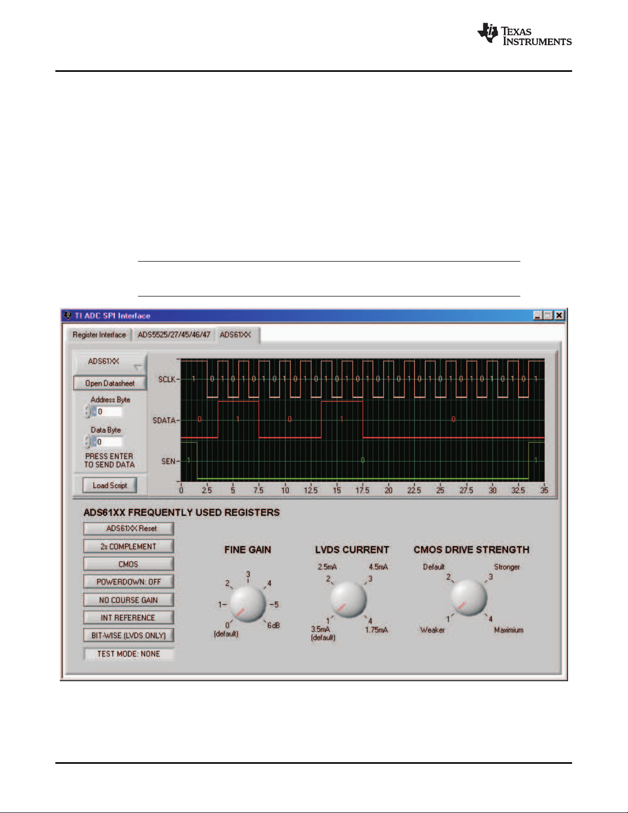
and it should automatically find the TI ADC SPI interface drivers. See Figure 1 .
Note: Before plugging in the USB cable for the first time, install the TI ADC SPI software. The
software installs the drivers necessary for USB communication.
®
operating system to search for device drivers,
www.ti.com
Figure 1. TI ADC SPC Interface Screen
10 SLAU206B – September 2007 – Revised April 2008
Submit Documentation Feedback
Page 11

www.ti.com
3.2 Setting Up the EVM for ADC SPI Control
Users who wish to use the ADC SPI interface must supply 5 VDC to J20, which provides power to the
USB circuit. By default, the EVM comes with the ADC configured in parallel mode. In order to use the SPI
interface to control the ADC modes of operation, users must move several jumpers.
• Move jumper J3 to short positions 1–2, which places the ADC into serial operation mode.
• Move jumper J7 to short positions 1–2, which allows the USB circuit to control SCLK.
• Move jumper J6 to short positions 1–2, which allows the USB circuit to control SDATA.
• Move jumper J2 to short positions 1–2, which allows the USB circuit to control SEN.
3.3 Using the TI ADC SPI Interface Software
Once the software is installed and the USB cable is connected, three primary modes of operating the
software are available: SPI Register Writes, SPI Register Write Using a Script File, and
ADS61xx/ADS61B23 Frequently Used Registers.
3.3.1 SPI Register Writes
The most basic mode of operation allows full control of writing to individual register addresses. In the top
left corner of the interface screen (Figure 1 ), select the ADS61xx ADC from the ADC SPI Protocol
drop-down list. Next, type the Address Bytes(s) in hexadecimal (hex) and Data Byte(s) in hex, which can
be found in the device data sheet. When you are ready to send this command to the ADC, press "Enter"
on your keyboard. The graph indicator is updated with the patterns sent to the ADC. The default inputs to
both the Address Byte(s) and Data Byte(s) fields are hex inputs as designated by the small x in the
control. Users can change the default input style by clicking on the "x" to binary, decimal, octal, or hex.
Multiple register writes can be written simply by changing the contents of the Address Byte(s) and Data
Byte(s) field and pressing Enter again.
TI ADC SPI Control Interface
3.3.2 SPI Register Write Using a Script File
For situations where the same multiple registers must be written on a frequent basis, users can easily use
a text editor to create a script file containing all ADC register writes. An example script file is located in the
\\Install Directory\Script Files\ADS6145_LVDS_CourseGain.txt. Users who wish to take advantage of
writing their own script files should start by using the ADS6145_LVDS_CourseGain.txt as a template file.
When ready to write the contents of the script file to the ADC, users can press the Load Script button and
they will be prompted for the file location of their script file. The commands are sent to the ADC when the
user acknowledges the selection of the file.
3.3.2.1 ADS61xx Frequently Used Registers
For ease of use, several buttons have been added that allow one-click register writes of commonly used
features found in Table 4 . These are found in the ADS61xx tab, as these commands are specific to the
ADS61xx ADC only. The software writes to the ADC both the contents of the associated address and data
when the button is clicked. When the ADS61xx Reset button is pressed, it issues a software reset to the
ADC, and it resets the button values to match the contents inside of the ADC. The graph indicator plots
the SPI commands written to the ADC when a button has been depressed.
SLAU206B – September 2007 – Revised April 2008 11
Submit Documentation Feedback
Page 12

TI ADC SPI Control Interface
ADS61xx Reset
2s Complement Straight Binary
CMOS DDR LVDS
Powerdown: OFF Powerdown On
No Course Gain 3.5-dB Course Gain
INT Reference EXT Reference
Bit-Wise (LVDS Only) Byte-Wise
Test Mode: None Multiple Options
www.ti.com
Table 4. ADS61xx Frequently Used Registers
Default Value Alternate Value
12 SLAU206B – September 2007 – Revised April 2008
Submit Documentation Feedback
Page 13

www.ti.com
4 Connecting to FPGA Platforms
The ADS61xx/ADS61B23 EVM provides several connection options to mate the EVM to various FPGA
development platforms and FPGA-based capture boards.
4.1 TSW1100
Using the accompanying CMOS breakout board, users can easily mate TI's TSW1100 capture board to
the ADS61xx/ADS61B23 EVM. Simply connect the breakout board to the J2 (Channel 2) connector on the
TSW1100. From an orientation standpoint, the Xilinx™ FPGA faces the ADC when correctly configured.
Before using the TSW1100 to capture ADC data for the first time, users should update the TSW1100
Supported_ADCs.txt file. They should explore the accompanying ADS61xx/ADS61B23 software CD and
replace the installed TSW1100 Supported_ADC.txt file with the one found on the CD; this file adds
TSW1100 support for both the ADS612x and ADS614x.
Finally, users should ensure that the ADC61xxEVM is configured in CMOS output mode. In addition, the
TSW1100 represents a load greater than 5 pF and as such, users should consider boosting the CMOS
drive strength by using the TI SPI Control software. In many cases, the boosting of the drive strength is
not required to perform valid data captures when using the TSW1100; this is an optional step.
4.2 TSW1200
The ADS61xx/ADS61B23 natively plugs into the TSW1200 FPGA platform. In most circumstances, the
TSW1200 functions as a deserializer. However, the Virtex™-4 FPGA can be reprogrammed to allow the
ultimate in flexible solution prototyping. For users wishing to apply FPGA control over the
ADS61xx/ADS61B23 SPI interface, move the surface-mount jumpers into the following positions.
• Move the jumper on J2 (SEN) to the 1–2 position, and remove R7 and populate R62 with a 0- Ω
resistor.
• Move the jumper on J7 (SCLK) to the 1–2 position, and remove R20 while installing the 0- Ω resistor to
R63.
• Move the jumper on J6 (SDATA) to the 1–2 position, and remove R19 while installing the 0- Ω resistor
to R64.
• Remove R18.
• Move the jumper on J3 to position 1–2 to configure the ADC into the SPI operation mode (serial
interface mode).
Connecting to FPGA Platforms
SLAU206B – September 2007 – Revised April 2008 13
Submit Documentation Feedback
Page 14

ADC Evaluation
5 ADC Evaluation
This section describes how to set up a typical ADC evaluation system that is similar to what TI uses to
perform testing for data-sheet generation. Consequently, the information in this section is generic in nature
and is applicable to all high-speed, high-resolution ADC evaluations. This section covers signal tone
analysis, which yields ADC data-sheet figures of merit such as signal-to-noise ratio (SNR) and spurious
free dynamic range (SFDR).
5.1 Hardware Selection
To reveal the true performance of the ADC under evaluation, great care should be taken in selecting both
the ADC signal source and ADC clocking source.
5.1.1 Analog Input Signal Generator
When choosing the quality of the ADC analog input source, consider both harmonic distortion performance
of the signal generator and the noise performance of the source.
In many cases, the harmonic distortion performance of the signal generator is inferior to that of the ADC,
and additional filtering is needed if users expect to reproduce the ADC SFDR numbers found in the data
sheet. Users can easily evaluate the harmonic distortion of the signal generator by hooking it directly to a
spectrum analyzer, measuring the power of the output signal, and comparing that to the power of the
integer multiples of the output signal frequency. If the harmonic distortion is worse than the ADC under
evaluation, the ADC digitizes the performance of the signal generator and the true SFDR of the ADC is
masked. To alleviate this, it is recommended that users provide additional LC filtering after the signal
generator output.
Another important metric when deciding on a signal generator is its noise performance. As with the
distortion performance, if the noise performance is worse than that of the ADC under evaluation, the ADC
digitizes the performance of the source. Noise can be broken into two components, broadband noise and
close-in phase noise. Broadband noise can be improved by the LC filter added to improve distortion
performance; however, the close-in phase noise typically cannot be improved by additional filtering.
Therefore, when selecting an analog signal source, it is important to review the manufacturer's phase
noise plots and take care to choose a signal generator with the best phase-noise performance.
www.ti.com
5.1.2 Clock Signal Generator
Equally important in the high-performance ADC evaluation setup is the selection of the clocking source.
Most modern ADCs, the ADS61xx/ADS61B23 included, accept either a sinusoidal or a square-wave clock
input. The key metric in selecting a clocking source is selecting a source with the lowest jitter. This
becomes increasingly important as the ADC input frequency (fin) increases, because the ADC SNR
evaluation setups can become jitter-limited (tj) as shown by the following equation.
In theory, a square-wave source with femtosecond jitter would be ideal for an ADC evaluation setup.
However, in practical terms, most commercially available square-wave generators offer jitter measured in
picoseconds, which is too great for high-resolution ADC evaluation setups. Therefore, most evaluation
setups rely on the ADC internal clock buffer to convert a sinusoidal input signal into a ultralow-jitter square
wave. When selecting a sinusoidal clocking source, it has been shown that phase noise has a direct
impact on jitter performance. Consequently, great scrutiny should be applied to the phase-noise
performance of the clocking signal generator. TI has found that high-Q monolithic crystal filters can
improve the phase noise of the signal generator, and these filters become essential elements of the
evaluation setup when high ADC input frequencies are being evaluated.
SNR (dBc) = 20 log (2 π × fin× tj(rms))
14 SLAU206B – September 2007 – Revised April 2008
Submit Documentation Feedback
Page 15

www.ti.com
5.2 Coherent Input Frequency Selection
Typical ADC analysis requires users to collect the resulting time-domain data and perform a Fourier
transform to analyze the data in the frequency domain. A stipulation of the Fourier transform is that the
signal must be continuous-time; however, this is impractical when looking at a finite set of ADC samples,
usually collected from a logic analyzer. Consequently, users typically apply a window function to minimize
the time-domain discontinuities that arise when analyzing a finite set of samples. For ADC analysis,
window functions have their own frequency signatures or lobes that distort both SNR and SFDR
measurements of the ADC.
TI uses the concept of coherent sampling to work around the use of a window function. The central
premise of coherent sampling entails that the input signal into the ADC is carefully chosen such that when
a continuous-time signal is reconstructed from a finite sample set, no time-domain discontinuities exist. To
achieve this, the input frequency must be an integer multiple of the ratio of the ADC sample rate (fs) and
the number of samples collected from the logic analyzer (N
the fundamental frequency (ff). Determining the ADC input frequency is a two-step process. First, the
users select the frequency of interest for evaluating the ADC; then, they divide this by the fundamental
frequency. This typically yields a non-integer value, which should be rounded to the nearest odd,
preferably prime, integer. Once that integer, or frequency bin (f
this with the fundamental frequency to obtain a coherent frequency to program into their ADC input signal
generator. The procedure is summarized as follows.
ff= fs/N
f
Coherent frequency = ff× f
s
= Odd_round(f
bin
ADC Evaluation
). The ratio of fsto N
s
), has been determined, users multiply
bin
/ff)
desired
bin
is typically referred to as
s
SLAU206B – September 2007 – Revised April 2008 15
Submit Documentation Feedback
Page 16

Physical Description
6 Physical Description
6.1 PCB Layout
www.ti.com
This section describes the physical characteristics and PCB layout of the EVM.
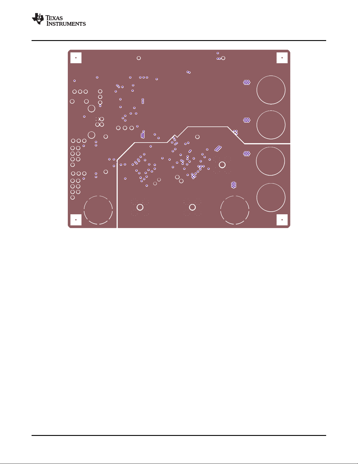
The EVM is constructed on a four-layer, 0.062-inch thick PCB using FR-4 material. The individual layers
are shown in Figure 2 through Figure 6 . The layout features a split ground plane; however, similar
performance can be obtained with careful layout using a common ground plane.
Figure 2. Top Silkscreen
16 SLAU206B – September 2007 – Revised April 2008
Submit Documentation Feedback
Page 17
www.ti.com
Physical Description
Figure 3. Component Side
SLAU206B – September 2007 – Revised April 2008 17
Submit Documentation Feedback
Page 18

Physical Description
www.ti.com
Figure 4. Ground Plane 1
18 SLAU206B – September 2007 – Revised April 2008
Submit Documentation Feedback
Page 19

www.ti.com
Physical Description
Figure 5. Power Plane 1
SLAU206B – September 2007 – Revised April 2008 19
Submit Documentation Feedback
Page 20

Physical Description
www.ti.com
Figure 6. Bottom Side
20 SLAU206B – September 2007 – Revised April 2008
Submit Documentation Feedback
Page 21

www.ti.com
6.2 Bill of Materials
Table 5. Bill of Materials
Qty Reference Not Part Foot Print Part Number Manufacturer
5 C1, C5, C8, C52, 33 µ F TANT_B B45196H2336M209 Kemet
C54
5 C2, C9, C30, C56, 10 µ F 805 ECJ-2FB0J106K Panasonic
C57
3 C3, C6, C31 1 µ F 603 ECJ-1VB1A105K Panasonic
43 C4, C7, 0.1 µ F 603 ECJ-1VB1C104K Panasonic
C11–C29,C32–C35,
C53, C55, C66,
C67, C70, C72,C74,
C75, C77–C79,C81,
C83, C85,
C87–C89, C92
4 C71, C73, C82, C84 10 µ F 805 ECJ-2FB1A106K Panasonic
1 C76 18 pF 603 ECJ-1VC1H180J Panasonic
1 C80 0.22 µ F 603 ECJ-1VB1A224K Panasonic
1 C86 10 µ F TANT_A T491A106M010AT Kemet
2 C90,C91 27 pF 603 GRM1885C2A270JA01D Murata
1 C93 0.01 µ F 603 C0603C103K1RACTU Kemet
0 JP1 Not HEADER 2/SM JUMPER2 NO PART
5 JP2–JP6 Jumper_1x3_SMT, Short pin SJP3_JUMPER NO PART
1 JP8 Jumper_1x3_SMT, Short pin SJP3_JUMPER NO PART
2 J1, J4 HEADER 4x2 hdr4X2_100ctr 90131-0124 Molex
4 J2, J3, J7, JP7 HMTSW-103-07-G-S-.240 HDR_THVT_1x3_100_M HMTSW-103-07-G-S-.240 Samtec
1 J6 HMTSW-103-07-G-S-.240 HDR_THVT_1x3_100_M HMTSW-103-07-G-S-.240 Samtec
1 J5 SMD3P_BRIDGE, Short pin smd_bridge_0603 NO PART
3 J8, J9, J15 SMA SMA_THVT_320x320 142-0701-201 Johnson Components
1 J10 CONN_QTH_30X2-D-A conn_QTH_30X2-D-A QTH-060-02-F-D-A Samtec
4 J11, J13, J16, J20 RED Banana Jack ST-351A ALLIED
2 J12, J14 BLK Banana Jack ST-351B ALLIED
1 J17 CONN USB TYP B FEM conn_usb_typb_fem 897-30-004-90-000 Milmax
5 L1–L3, L8, L9 68 603 MI0603J680R-10 Steward
1 L10 1 k at 100 MHz 805 BLM21AG102SN1D Murata
6 R3–R5, R9, R11, 1 k Ω 603 ERJ-3EKF1001V Panasonic
R14
5 R6, R10, R15, R18, 10 k Ω 603 ERJ-3EKF1002V Panasonic
R35
4 R7, R26, R57, 0 Ω 603 ERJ-3GEY0R00V Panasonic
8 R8, R12, R13, R17, 100 Ω 603 ERJ-3EKF1000V Panasonic
1 R16 10 Ω 603 ERJ-3EKF10R0V Panasonic
2 R22, R25 200 Ω 603 ERJ-3EKF2000V Panasonic
2 R23, R24 39 Ω 603 RC0603FR-0739RL Panasonic
0 R27, R28 Not 121 Ω 603 ERJ-3EKF1210V Panasonic
5 R29, R31, R38, 49.9 Ω 603 ERJ-3EKF49R9V Panasonic
1 R30 60.4 k Ω 603 ERJ-3EKF6042V Panasonic
2 R32, R34 10 Ω 603 ERJ-3EKF10R0V Panasonic
(1)
(1)
R66
R19, R20, R40, R44
R46, R47
Remove R66 for the ADS61B23 EVM.
Installed
installed
1 and 2 with 0 Ω
2 and 3 with 0 Ω
1 and 2 with 0 Ω
installed
Physical Description
ELECTRONICS
ELECTRONICS
SLAU206B – September 2007 – Revised April 2008 21
Submit Documentation Feedback
Page 22

Physical Description
Table 5. Bill of Materials (continued)
Qty Reference Not Part Foot Print Part Number Manufacturer
0 R33 Not 200 Ω 402 ERJ-2RKF2000X Panasonic
2 R36, R48 348 Ω 603 ERJ-3EKF3480V Panasonic
0 R37, R45 Not 499 Ω 603 ERJ-3EKF4990V Panasonic
2 R39, R43 69.8 Ω 603 ERJ-3EKF69R8V Panasonic
0 R41, R42 Not 200 Ω 603 ERJ-3EKF2000V Panasonic
1 R49 10 k Ω 603 ERJ-3GEYJ103V Panasonic
1 R50 2.21 k Ω 603 ERJ-3EKF2211V Panasonic
1 R51 4.7 k Ω 603 ERJ-3EKF4R71V Panasonic
0 R52 Not 10 k Ω 603 ERJ-3EKF1002V Panasonic
1 R53 1.5 k Ω 603 ERJ-3EKF1501V Panasonic
0 R21, R54, R62–R64 Not 0 Ω 603 ERJ-3GEY0R00V Panasonic
2 R55, R56 26.7 Ω 603 ERJ-3EKF26R7V Panasonic
2 R58, R60 130 Ω 603 ERJ-3EKF1300V Panasonic
2 R59, R61 82.5 Ω 603 ERJ-3EKF82R5V Panasonic
1 R65 0 Ω 1206 ERJ-S080R00V Panasonic
1 SW1 SW PUSHBUTTON SW_RESET_PTS635 PTS635SL43 C & K Switch
3 TP1, TP3, TP6 Test Point Black testpoint 5001 Keystone
3 TP2, TP4, TP5 Test Point White testpoint 5002 Keystone
0 TP7–TP9 Not T POINT R TESTPOINT 5002 Keystone
2 T1, T2 TC4-1W XFMR_TC4-1W TC4-1W Mini Circuits
1 T3 TC1-1T XFMR_TC4-1W TC1-1T Mini Circuits
1 U1 ADS614X QFN32 TI
1 U2 CDCP1803 mlf_qfn_24 CDCP1803RGET TI
1 U10 TPS73233 DBV5 TPS73233DBVT TI
1 U11 THS4509 QFN16 THS4509RGTT TI
1 U13 93C66B TSSOP8 93C66B Microchip
1 U14 FT245BM PQFP32 FT245BM Future Technology
1 Y1 6.0000MHz smd_csm-7_xtal ECS-60-32-5PDN-TR ECS
4 MP2 Screw machine, ph 4-40 × PMS 440 0038 PH Building Fasteners
4 MP3 Stand-off hex .5/4-40THR 1902C Keystone Electronic
Installed
installed
installed
installed
installed
installed
installed
3/8
www.ti.com
Devices
22 SLAU206B – September 2007 – Revised April 2008
Submit Documentation Feedback
Page 23

PD
VREF1
SIGNAL_IN
+5V_AMP
-VSS_AMP
+5V_AMP
AGND
AMP+
AMP-
AMP+
AMP-
VREF
SH2
IN_M
SH2
IN_P SH2
VREF
SH2
Default:Short2-3
Default:Short1-2
Default:Short1-2
R26
0OHM
R26
0OHM
R44
100
R44
100
C76
18pF
C76
18pF
T1
TC4-1WT1TC4-1W
3
2
1
6
5
4
C34
.1uF
C34
.1uF
1
2
R43
69.8
R43
69.8
R37
499
DoNotInstall
R37
499
DoNotInstall
R46
49.9
R46
49.9
C71
10uF
10V
C71
10uF
10V
12
C70
.1uF
16V
C70
.1uF
16V
C35
.1uF
C35
.1uF
1
2
R35
10K
1/10W
1%
R35
10K
1/10W
1%
C79
.1uF
16V
C79
.1uF
16V
C77
.1uF
C77
.1uF
R45
499
DoNotInstall
R45
499
DoNotInstall
R66
0OHM
R66
0OHM
C14
.1uF
C14
.1uF
1
2
R36
348
R36
348
C80
.22uF
C80
.22uF
R33
200
DoNotInstall
R33
200
DoNotInstall
C75
.1uF
C75
.1uF
MS A
DEN
J8
AIN
MS A
DEN
J8
AIN
1
5234
C74
.1uF
16V
C74
.1uF
16V
R47
49.9
R47
49.9
R57
0OHM
R57
0OHM
R39
69.8
R39
69.8
R32
10
1/16W
1%
R32
10
1/16W
1%
JP7JP7
1
3
2
U11
THS4509
U11
THS4509
NC1VIN-2CM1
4
VS+
5
VS+
6
VOUT+
3
VS+
7
VS+
8
CM2
9
VOUT-
10
VIN+
11
PD
12
VS-
13
VS-
14
VS-
15
VS-
16
PAD
17
R24
39
1/10W
1%
R24
39
1/10W
1%
R40
100
R40
100
T2
TC4-1WT2TC4-1W
3
2
1
6
5
4
MS A
DEN
J15
AMP
MS A
DEN
J15
AMP
1
5234
C15
.1uF
16V
C15
.1uF
16V
C72
.1uF
16V
C72
.1uF
16V
C82
10uF
10V
C82
10uF
10V
12
R25
200
R25
200
C73
10uF
10V
C73
10uF
10V
12
R48
348
R48
348
R22
200
R22
200
C78
.1uF
16V
C78
.1uF
16V
R38
49.9
R38
49.9
R42
200
DoNotInstall
R42
200
DoNotInstall
R34
10
1/16W 1%
R34
10
1/16W 1%
C81
.1uF
16V
C81
.1uF
16V
JP6JP6
1
3
2
JP5JP5
1
3
2
R21
0OHM
DoNotInstall
R21
0OHM
DoNotInstall
R41
200
DoNotInstall
R41
200
DoNotInstall
C84
10uF
10V
C84
10uF
10V
12
C83
.1uF
16V
C83
.1uF
16V
R23
39
1/10W
1%
R23
39
1/10W
1%
RemoveR66
for ADS61B23
www.ti.com
Physical Description
6.3 EVM Schematics
Figure 7. EVM Schematic, Sheet 1
SLAU206B – September 2007 – Revised April 2008 23
Submit Documentation Feedback
Page 24

ICLKP
ICLKM
SEN
SDA
SCLOCK
PDWN
SEN
RESET
SCLOCK
+3.3VD
+3.3VA
+3.3VD
+3.3VD
+3.3VD
+3.3VD
+3.3VD
+3.3VD
IN_M
SH1
IN_P
SH1
D2_D3_P SH4
D0_D1_P SH4
D0_D1_M SH4
D2_D3_M SH4
D4_D5_P SH4
D4_D5_M
SH4
D6_D7_P SH4
D6_D7_M
SH4
ICLKP
SH3
ICLKM
SH3
ADCRESETSH5
SDATASH5
VREF
SH1
PDN SH5
CS SH5
SCLK SH5
FPGA_SEN SH4
FPGA_SCLK SH4
FPGA_SDATASH4
CLKOUTP
SH4
CLKOUTM
SH4
D8_D9_P
SH4
D8_D9_M
SH4
D10_D11_P
SH4
D10_D1
1_M
SH4
D12_D13_P
SH4
D12_D13_M
SH4
PARALLELINTERFACE
SERIALINTERFACE
Default:Shunt2-3
Default:Shunt1-2
Default:Shunt2-3
Default:Shunt2-3
R17
100
R17
100
1
2
R111KR11
1K
12
R10
10K
R10
10K
12
TP5TP5
R6
10KR610K
12
R20
100
R20
100
1
2
SW1SW1
C13
.1uF
C13
.1uF
12
J4J4
246
8
135
7
R141KR14
1K
12
R8
100R8100
1
2
J2J2
123
U1
ADS614XU1ADS614X
DRVDD1RESET2SCLK3SDATA4SEN5AGND6CLKP7CLKM
8
AGND
9
INP
10
INM
11
AGND
12
AVDD
13
CM_REFIN
14
AVDD_FVDD
15
PDN
16
D0_D1_M
17
D0_D1_P
18
D2_D3_M
19
D2_D3_P
20
D4_D5_M
21
D4_D5_P
22
D6_D7_M
23
D6_D7_P
24
CLKOUTM
25
CLKOUTP
26
D8_D9_M
27
D8_D9_P
28
D10_D11_M
29
D10_D11_P
30
D12_D13_M
31
D12_D13_P
32
DRVSS(GNDPAD)
33
R64
0OHM
DoNotInstall
R64
0OHM
DoNotInstall
J7J7
123
TP6TP6
R7
0OHMR70OHM
R91KR9
1K
12
R18
10K
R18
10K
12
C12
.1uF
C12
.1uF
12
TP1TP1
R19
100
R19
100
1
2
R13
100
R13
100
1 2
TP3TP3
TP2TP2
R15
10K
R15
10K
12
C85
.1uF
C85
.1uF
12
R62
0OHM
DoNotInstall
R62
0OHM
DoNotInstall
J1J1
246
8
135
7
J3J3
123
TP4TP4
C11
.1uF
C11
.1uF
12
J6J6
123
R31KR3
1K
12
R12
100
R12
100
1
2
R51KR5
1K
12
J5J5
123
R63
0OHM
DoNotInstall
R63
0OHM
DoNotInstall
R41KR4
1K
12
R1610R16
10
Physical Description
www.ti.com
Figure 8. EVM Schematic, Sheet 2
24 SLAU206B – September 2007 – Revised April 2008
Submit Documentation Feedback
Page 25

ADCCLK-
CLKOUT\
CLKOUT
ADCCLK+
CLK-
CLK+
+3.3V_AUX
+3.3V_AUX
+3.3V_AUX
CDC_CLKM SH4
CDC_CLKP SH4
ICLKP
SH2
ICLKM SH2
Default:Short2-3
Default:Short1-2
Default:Short1-2
Default:Short1-2
R29
49.9
1/10W
1%
R29
49.9
1/10W
1%
C16
.1uF
16V
C16
.1uF
16V
1
2
R60
130
R60
130
1 2
C32
.1uF
16V
C32
.1uF
16V
1
2
R31
49.9
R31
49.9
JP8JP8
123
R28
121
1/10W
DoNotInstall
1%
R28
121
1/10W
DoNotInstall
1%
R58
130
R58
130
1 2
MSA
D EN
J9
CLK
MSA
D EN
J9
CLK
1
5234
C19
.1uF
16V
C19
.1uF
16V
C29
.1uF
C29
.1uF
1 2
C28
.1uF
C28
.1uF
1 2
C27
.1uF
C27
.1uF
1 2
C20
.1uF
C20
.1uF
1
2
C26
.1uF
C26
.1uF
1 2
C25
.1uF
C25
.1uF
1 2
JP4JP4
123
R27
121
1/10W
DoNotInstall
1%
R27
121
1/10W
DoNotInstall
1%
C24
.1uF
C24
.1uF
1 2
R59
82.5
R59
82.5
U2
CDCM1803
U2
CDCM1803
IN
4
VSS
7
VDDPECL
5
Y115Y1
16
VDD117VDD1
14
EN1VDDPECL2IN
3
VSS
13
VBB
6
VDD2
8
Y2
9
Y2
10
VDD2
11
NC
12
S0
18
S1
19
VDD0
20
Y0
21
Y0
22
VDD0
23
S2
24
GND
25
C23
.1uF
C23
.1uF
1 2
T3
TC1-1TT3TC1-1T
3
2
1
6
5
4
C18
.1uF
16V
C18
.1uF
16V
1
2
C33
.1uF
16V
C33
.1uF
16V
1
2
C22
.1uF
C22
.1uF
1 2
C21
.1uF
C21
.1uF
1 2
JP3JP3
123
R30
60.4K
R30
60.4K
JP2JP2
123
R61
82.5
R61
82.5
C17
.1uF
16V
C17
.1uF
16V
JP1
DoNotInstall
JP1
DoNotInstall
1
2
www.ti.com
Physical Description
Figure 9. EVM Schematic, Sheet 3
SLAU206B – September 2007 – Revised April 2008 25
Submit Documentation Feedback
Page 26

D12_D13_PSH2
D12_D13_MSH2
D10_D11_PSH2
D10_D11_MSH2
D8_D9_PSH2
D8_D9_MSH2
CLKOUTPSH2
CLKOUTMSH2
D6_D7_PSH2
D6_D7_MSH2
D4_D5_PSH2
D4_D5_MSH2
D2_D3_PSH2
D2_D3_MSH2
D0_D1_PSH2
D0_D1_MSH2
CDC_CLKPSH3
CDC_CLKMSH3
FPGA_SCLK SH2
FPGA_SEN SH2
FPGA_SDATA SH2
J10
CONN_QTH_30X2-D-A
J10
CONN_QTH_30X2-D-A
2
4
6
8
10
12
14
16
18
20
22
24
26
28
30
32
34
36
38
40
1
3
5
7
9
11
13
15
17
19
21
23
25
27
29
31
33
35
37
39
G1G2
G3G4
G5G6
G7G8
4142
4344
4546
4748
4950
5152
5354
5556
5758
5960
6162
6364
6566
6768
6970
7172
7374
7576
7778
7980
8182
8384
8586
8788
8990
9192
9394
9596
9798
99100
101102
103104
105106
107108
109110
111112
113114
115116
117118
119120
Physical Description
26 SLAU206B – September 2007 – Revised April 2008
Figure 10. EVM Schematic, Sheet 4
Submit Documentation Feedback
www.ti.com
Page 27

+3.3VD_IN
5V_IN
+3.3VA_IN
+3.3V
A
+3.3VD
5V
+5V_AMP
C3
1uFC31uF
12
C4
.1uFC4.1uF
12
J13
RED
+3.3VA_IN
J13
RED
+3.3VA_IN
C30
10uF
6.3V
C30
10uF
6.3V
12
L168L1
68
1
2
+
C8
33uF+C8
33uF
12
+
C52
33UF
10V
+
C52
33UF
10V
12
+
C1
33uF+C1
33uF
12
L268L2
68
1
2
C53
.1uF
16V
C53
.1uF
16V
+
C5
33uF+C5
33uF
12
J20
RED
+5V_IN
J20
RED
+5V_IN
C31
1uF
10V
C31
1uF
10V
12
C6
1uFC61uF
12
J11
RED
+3.3VD_IN
J11
RED
+3.3VD_IN
R65
0OHM
R65
0OHM
J14
BLK
GND
J14
BLK
GND
C7
.1uFC7.1uF
12
C9
10uF
6.3V
C9
10uF
6.3V
12
L868L8
68
1
2
C57
10uF
6.3V
C57
10uF
6.3V
12
L368L3
68
1
2
J12
BLK
GND
J12
BLK
GND
C2
10uF
6.3V
C2
10uF
6.3V
12
-5V_IN
+3.3V_AUX
5V
-VSS_AMP
C67
.1uF
16V
C67
.1uF
16V
C55
.1uF
16V
C55
.1uF
16V
C66
.1uF
16V
C66
.1uF
16V
J16
RED
-VSS_AMP
J16
RED
-VSS_AMP
L968L9
68
1
2
U10
TPS73233
U10
TPS73233
EN
3
IN1GND
2
OUT
5
NC/FB
4
C56
10uF
6.3V
C56
10uF
6.3V
1 2
+
C54
33UF
10V
+
C54
33UF
10V
12
www.ti.com
Physical Description
Figure 11. EVM Schematic, Sheet 5
SLAU206B – September 2007 – Revised April 2008 27
Submit Documentation Feedback
Page 28
GND
D6
D9
D1
D3
D7
D5
CLK
D13
D0
D2
D8
D10
D12
D11
D4
D7
D6
D5
D4
D3
D2
D1
D0
D13
D12
D11
D10
D9
D8
CLK
J1
CONN_QSH_30X2-D-A
J1
CONN_QSH_30X2-D-A
2
4
6
8
10
12
14
16
18
20
22
24
26
28
30
32
34
36
38
40
1
3
5
7
9
11
13
15
17
19
21
23
25
27
29
31
33
35
37
39
G1G2
G3G4
G5G6
G7G8
4142
4344
4546
4748
4950
5152
5354
5556
5758
5960
6162
6364
6566
6768
6970
7172
7374
7576
7778
7980
8182
8384
8586
8788
8990
9192
9394
9596
9798
99100
101102
103104
105106
107108
109110
111112
113114
115116
117118
119120
J2
40PINIDC
DATA_OUT
J2
40PINIDC
DATA_OUT
1 2
4
6
8
10
12
14
16
18
20
22
24
26
28
30
32
3
5
7
9
11
13
15
17
19
21
23
25
27
29
31
33 34
35 36
37 38
39 40
Physical Description
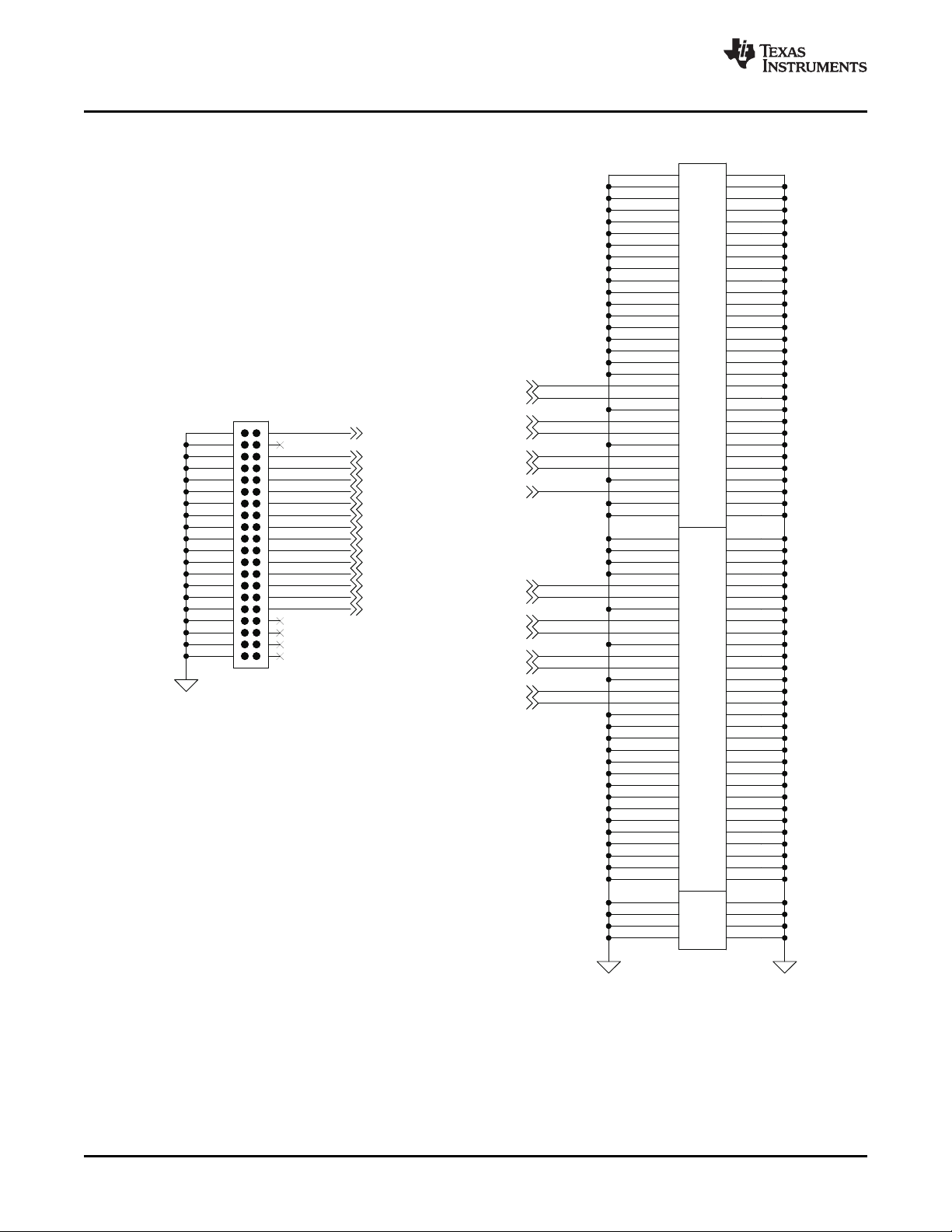
Figure 12. Breakout Board Schematic, Sheet 6
28 SLAU206B – September 2007 – Revised April 2008
Submit Documentation Feedback
www.ti.com
Page 29

EVALUATION BOARD/KIT IMPORTANT NOTICE
Texas Instruments (TI) provides the enclosed product(s) under the following conditions:
This evaluation board/kit is intended for use for ENGINEERING DEVELOPMENT, DEMONSTRATION, OR EVALUATION PURPOSES
ONLY and is not considered by TI to be a finished end-product fit for general consumer use. Persons handling the product(s) must have
electronics training and observe good engineering practice standards. As such, the goods being provided are not intended to be complete
in terms of required design-, marketing-, and/or manufacturing-related protective considerations, including product safety and environmental
measures typically found in end products that incorporate such semiconductor components or circuit boards. This evaluation board/kit does
not fall within the scope of the European Union directives regarding electromagnetic compatibility, restricted substances (RoHS), recycling
(WEEE), FCC, CE or UL, and therefore may not meet the technical requirements of these directives or other related directives.
Should this evaluation board/kit not meet the specifications indicated in the User’s Guide, the board/kit may be returned within 30 days from
the date of delivery for a full refund. THE FOREGOING WARRANTY IS THE EXCLUSIVE WARRANTY MADE BY SELLER TO BUYER
AND IS IN LIEU OF ALL OTHER WARRANTIES, EXPRESSED, IMPLIED, OR STATUTORY, INCLUDING ANY WARRANTY OF
MERCHANTABILITY OR FITNESS FOR ANY PARTICULAR PURPOSE.
The user assumes all responsibility and liability for proper and safe handling of the goods. Further, the user indemnifies TI from all claims
arising from the handling or use of the goods. Due to the open construction of the product, it is the user’s responsibility to take any and all
appropriate precautions with regard to electrostatic discharge.
EXCEPT TO THE EXTENT OF THE INDEMNITY SET FORTH ABOVE, NEITHER PARTY SHALL BE LIABLE TO THE OTHER FOR ANY
INDIRECT, SPECIAL, INCIDENTAL, OR CONSEQUENTIAL DAMAGES.
TI currently deals with a variety of customers for products, and therefore our arrangement with the user is not exclusive.
TI assumes no liability for applications assistance, customer product design, software performance, or infringement of patents or
services described herein.
Please read the User’s Guide and, specifically, the Warnings and Restrictions notice in the User’s Guide prior to handling the product. This
notice contains important safety information about temperatures and voltages. For additional information on TI’s environmental and/or
safety programs, please contact the TI application engineer or visit www.ti.com/esh .
No license is granted under any patent right or other intellectual property right of TI covering or relating to any machine, process, or
combination in which such TI products or services might be or are used.
FCC Warning
This evaluation board/kit is intended for use for ENGINEERING DEVELOPMENT, DEMONSTRATION, OR EVALUATION PURPOSES
ONLY and is not considered by TI to be a finished end-product fit for general consumer use. It generates, uses, and can radiate radio
frequency energy and has not been tested for compliance with the limits of computing devices pursuant to part 15 of FCC rules, which are
designed to provide reasonable protection against radio frequency interference. Operation of this equipment in other environments may
cause interference with radio communications, in which case the user at his own expense will be required to take whatever measures may
be required to correct this interference.
EVM WARNINGS AND RESTRICTIONS
It is important to operate this EVM within the input voltage range of–0.3 V to 3.6 V and the output voltage range of –0.3 V to 3.6 V.
Exceeding the specified input range may cause unexpected operation and/or irreversible damage to the EVM. If there are questions
concerning the input range, please contact a TI field representative prior to connecting the input power.
Applying loads outside of the specified output range may result in unintended operation and/or possible permanent damage to the EVM.
Please consult the EVM User's Guide prior to connecting any load to the EVM output. If there is uncertainty as to the load specification,
please contact a TI field representative.
During normal operation, some circuit components may have case temperatures greater than 50 ° C. The EVM is designed to operate
properly with certain components above 25 ° C as long as the input and output ranges are maintained. These components include but are
not limited to linear regulators, switching transistors, pass transistors, and current sense resistors. These types of devices can be identified
using the EVM schematic located in the EVM User's Guide. When placing measurement probes near these devices during operation,
please be aware that these devices may be very warm to the touch.
Mailing Address: Texas Instruments, Post Office Box 655303, Dallas, Texas 75265
Copyright 2007-2008, Texas Instruments Incorporated
Page 30

IMPORTANT NOTICE
Texas Instruments Incorporated and its subsidiaries (TI) reserve the right to make corrections, modifications, enhancements, improvements,
and other changes to its products and services at any time and to discontinue any product or service without notice. Customers should
obtain the latest relevant information before placing orders and should verify that such information is current and complete. All products are
sold subject to TI’s terms and conditions of sale supplied at the time of order acknowledgment.
TI warrants performance of its hardware products to the specifications applicable at the time of sale in accordance with TI’s standard
warranty. Testing and other quality control techniques are used to the extent TI deems necessary to support this warranty. Except where
mandated by government requirements, testing of all parameters of each product is not necessarily performed.
TI assumes no liability for applications assistance or customer product design. Customers are responsible for their products and
applications using TI components. To minimize the risks associated with customer products and applications, customers should provide
adequate design and operating safeguards.
TI does not warrant or represent that any license, either express or implied, is granted under any TI patent right, copyright, mask work right,
or other TI intellectual property right relating to any combination, machine, or process in which TI products or services are used. Information
published by TI regarding third-party products or services does not constitute a license from TI to use such products or services or a
warranty or endorsement thereof. Use of such information may require a license from a third party under the patents or other intellectual
property of the third party, or a license from TI under the patents or other intellectual property of TI.
Reproduction of TI information in TI data books or data sheets is permissible only if reproduction is without alteration and is accompanied
by all associated warranties, conditions, limitations, and notices. Reproduction of this information with alteration is an unfair and deceptive
business practice. TI is not responsible or liable for such altered documentation. Information of third parties may be subject to additional
restrictions.
Resale of TI products or services with statements different from or beyond the parameters stated by TI for that product or service voids all
express and any implied warranties for the associated TI product or service and is an unfair and deceptive business practice. TI is not
responsible or liable for any such statements.
TI products are not authorized for use in safety-critical applications (such as life support) where a failure of the TI product would reasonably
be expected to cause severe personal injury or death, unless officers of the parties have executed an agreement specifically governing
such use. Buyers represent that they have all necessary expertise in the safety and regulatory ramifications of their applications, and
acknowledge and agree that they are solely responsible for all legal, regulatory and safety-related requirements concerning their products
and any use of TI products in such safety-critical applications, notwithstanding any applications-related information or support that may be
provided by TI. Further, Buyers must fully indemnify TI and its representatives against any damages arising out of the use of TI products in
such safety-critical applications.
TI products are neither designed nor intended for use in military/aerospace applications or environments unless the TI products are
specifically designated by TI as military-grade or "enhanced plastic." Only products designated by TI as military-grade meet military
specifications. Buyers acknowledge and agree that any such use of TI products which TI has not designated as military-grade is solely at
the Buyer's risk, and that they are solely responsible for compliance with all legal and regulatory requirements in connection with such use.
TI products are neither designed nor intended for use in automotive applications or environments unless the specific TI products are
designated by TI as compliant with ISO/TS 16949 requirements. Buyers acknowledge and agree that, if they use any non-designated
products in automotive applications, TI will not be responsible for any failure to meet such requirements.
Following are URLs where you can obtain information on other Texas Instruments products and application solutions:
Products Applications
Amplifiers amplifier.ti.com Audio www.ti.com/audio
Data Converters dataconverter.ti.com Automotive www.ti.com/automotive
DSP dsp.ti.com Broadband www.ti.com/broadband
Clocks and Timers www.ti.com/clocks Digital Control www.ti.com/digitalcontrol
Interface interface.ti.com Medical www.ti.com/medical
Logic logic.ti.com Military www.ti.com/military
Power Mgmt power.ti.com Optical Networking www.ti.com/opticalnetwork
Microcontrollers microcontroller.ti.com Security www.ti.com/security
RFID www.ti-rfid.com Telephony www.ti.com/telephony
RF/IF and ZigBee® Solutions www.ti.com/lprf Video & Imaging www.ti.com/video
Mailing Address: Texas Instruments, Post Office Box 655303, Dallas, Texas 75265
Copyright © 2008, Texas Instruments Incorporated
Wireless www.ti.com/wireless
 Loading...