CLKINP, CLKINM
DAP, DAMINAP, INAM
PLL
x10/x20
DCP, DCM
DDP, DDM
INBP. INAM
INCP, INCM
INDP, INDM
DBP, DBM
JESD204B
SYNCbCD
SYSREFP, SYSREFM
RESET
SCAN_EN
SCLK
SEN
SDIN
SDOUT
Configuration
Registers
2x Decimation
High Pass/
Low Pass
2x Decimation
High Pass/
Low Pass
2x Decimation
High Pass/
Low Pass
2x Decimation
High Pass/
Low Pass
SYNCbAB
TRIGAB
TRIGCD
TRDYCD
JESD204B
TRDYAB
Burst Mode
Burst Mode
N
14bit
ADC
14-bit
ADC
14bit
ADC
14-bit
ADC
14bit
ADC
14bit
ADC
14-bit
ADC
14-bit
ADC
CLK
DIV
/2, /4
N
NCO
NCO
Product
Folder
Order
Now
Technical
Documents
Tools &
Software
Support &
Community
SBAS807A –JANUARY 2017–REVISED JANUARY 2017
ADS58J64 Quad-Channel, 14-Bit, 1-GSPS Telecom Receiver Device
ADS58J64
1 Features
1
• Quad Channel
• 14-Bit Resolution
• Maximum Sampling Rate: 1 GSPS
• Maximum Output Sample Rate: 500 MSPS
• Analog Input Buffer With High-Impedance Input
• Input 3-dB Bandwidth: 1 GHz
• Output Options:
– Rx: Decimate-by-2 and -4 Options With
Low-Pass Filter
– 200-MHz Complex Bandwidth or 100-MHz
Real Bandwidth Support
– DPD FB: 2x Decimation With 14-Bit Burst
Mode Output
• 1.1-VPPDifferential Full-Scale Input
• JESD204B Interface:
– Subclass 1 Support
– 1 Lane per ADC Up to 10 Gbps
– Dedicated SYNC Pin for Pair of Channels
• Support for Multi-Chip Synchronization
• 72-Pin VQFN Package (10 mm × 10 mm)
• Power Dissipation: 625 mW/Ch
• Spectral Performance
(Burst Mode, High Resolution):
– fIN= 190 MHz IF at –1 dBFS:
– SNR: 69 dBFS
– NSD: –153 dBFS/Hz
– SFDR: 86 dBc (HD2, HD3),
95 dBFS (Non HD2, HD3)
– fIN= 370 MHz IF at –3 dBFS:
– SNR: 68.5 dBFS
– NSD: –152.5 dBFS/Hz
– SFDR: 80 dBc (HD2, HD3),
86 dBFS (Non HD2, HD3)
3 Description
The ADS58J64 is a low-power, wide-bandwidth, 14bit, 1-GSPS, quad-channel, telecom receiver device.
The ADS58J64 supports a JESD204B serial interface
with data rates up to 10 Gbps with one lane per
channel. The buffered analog input provides uniform
input impedance across a wide frequency range and
minimizes sample-and-hold glitch energy. The
ADS58J64 provides excellent spurious-free dynamic
range (SFDR) over a large input frequency range with
very low power consumption. The digital signal
processing block includes complex mixers followed
by low-pass filters with decimate-by-2 and -4 options
supporting up to a 200-MHz receive bandwidth. The
ADS58J64 also supports a 14-bit, 500-MSPS output
in burst mode, making the device suitable for a digital
pre-distortion (DPD) observation receiver.
The JESD204B interface reduces the number of
interface lines, thus allowing high system integration
density. An internal phase-locked loop (PLL)
multiplies the incoming analog-to-digital converter
(ADC) sampling clock to derive the bit clock that is
used to serialize the 14-bit data from each channel.
Device Information
PART NUMBER PACKAGE BODY SIZE (NOM)
ADS58J64 VQFN (72) 10.00 mm × 10.00 mm
(1) For all available packages, see the orderable addendum at
the end of the data sheet.
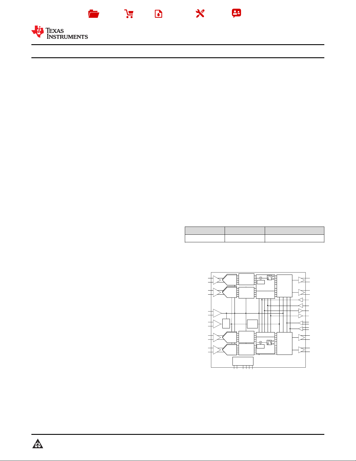
Simplified Block Diagram
(1)
2 Applications
• Multi-Carrier GSM Cellular Infrastructure
• Multi-Carrier Multi-Mode Cellular Infrastructure
• Telecommunications Receivers
• Telecom DPD Observation Receivers
1
Base Stations
Base Stations
An IMPORTANT NOTICE at the end of this data sheet addresses availability, warranty, changes, use in safety-critical applications,
intellectual property matters and other important disclaimers. PRODUCTION DATA.

ADS58J64
SBAS807A –JANUARY 2017–REVISED JANUARY 2017
www.ti.com
Table of Contents
1 Features.................................................................. 1
2 Applications ........................................................... 1
3 Description ............................................................. 1
4 Revision History..................................................... 2
5 Pin Configuration and Functions......................... 3
6 Specifications......................................................... 5
6.1 Absolute Maximum Ratings ...................................... 5
6.2 ESD Ratings ............................................................ 5
6.3 Recommended Operating Conditions....................... 6
6.4 Thermal Information.................................................. 6
6.5 Electrical Characteristics........................................... 7
6.6 AC Performance........................................................ 8
6.7 Digital Characteristics ............................................. 10
6.8 Timing Characteristics............................................. 11
6.9 Typical Characteristics: 14-Bit Burst Mode............. 12
6.10 Typical Characteristics: Mode 2............................ 18
6.11 Typical Characteristics: Mode 0............................ 19
7 Detailed Description............................................ 20
7.1 Overview ................................................................. 20
7.2 Functional Block Diagram ....................................... 20
7.3 Feature Description................................................. 21
7.4 Device Functional Modes........................................ 22
7.5 Programming........................................................... 32
7.6 Register Maps ........................................................ 39
8 Application and Implementation ........................ 66
8.1 Application Information............................................ 66
8.2 Typical Application .................................................. 73
9 Power Supply Recommendations...................... 74
10 Layout................................................................... 75
10.1 Layout Guidelines ................................................. 75
10.2 Layout Example .................................................... 75
11 Device and Documentation Support ................. 76
11.1 Receiving Notification of Documentation Updates 76
11.2 Community Resources.......................................... 76
11.3 Trademarks ........................................................... 76
11.4 Electrostatic Discharge Caution............................ 76
11.5 Glossary ................................................................ 76
12 Mechanical, Packaging, and Orderable
Information........................................................... 76
4 Revision History
NOTE: Page numbers for previous revisions may differ from page numbers in the current version.
Changes from Original (January 2017) to Revision A Page
• Changed Sample to Sampling in third Features bullet .......................................................................................................... 1
• Changed Bandwitdth: 250 MHz to Sample Rate: 500 MSPS in fourth Features bullet ......................................................... 1
• Added Input 3-dB Bandwidth bullet to Features section........................................................................................................ 1
• Changed plot and SNR and SFDR conditions of Figure 9 .................................................................................................. 13
• Added for loading trims to description of bit 1 in Register 64h Field Descriptions .............................................................. 45
• Changed select to set in description of bits 7-0 in Register 8Dh Field Descriptions and Register 8Eh Field Descriptions. 45
• Changed select to set in description of bits 7-0 in Register 8Fh Field Descriptions and Register 90h Field Descriptions.. 46
• Added Others: Do not use to Description column of Register 71h Field Descriptions and Register 72h Field
Descriptions.......................................................................................................................................................................... 50
• Changed Others: Do not use to Description column of Register 93h Field Descriptions and Register 94h Field
Descriptions.......................................................................................................................................................................... 51
• Added Valid only when CTRL_LID = 1 to description of bits 7-4 in Register 2Dh Field Descriptions ................................. 57
• Changed Description column of Register 41h Field Descriptions........................................................................................ 61
• Changed 1 : to 3 : and added Others: Do not use to Description column of Register 42h Field Descriptions ................... 61
• Changed description of bits 7-0 in Register 07h Field Descriptions..................................................................................... 65
• Changed description of bits 7-0 in Register 08h Field Descriptions ................................................................................... 65
2
Submit Documentation Feedback Copyright © 2017, Texas Instruments Incorporated
Product Folder Links: ADS58J64
72 SYNCbCDP19INCP
1TRDYCD 54 TRDYAB
71 SYNCbCDM20AVDD
2TRIGCD 53 TRIGAB
70 DVDD21AGND
3DGND 52 DGND
69 DDP22NC
4DVDD 51 DVDD
68 DDM23NC
5SDIN 50 PDN
67 DGND24AVDD19
6SCLK 49 RES
66 DCP25AVDD
7SEN 48 RESET
65 DCM26AGND
8DVDD 47 DVDD
64 DVDD27CLKINP
9AVDD 46 AVDD
63 DGND28CLKINM
10AVDD19 45 AVDD19
62 DBM29AGND
11SDOUT 44 AVDD
61 DBP30AVDD
12AVDD 43 AVDD
60 DGND31AVDD19
13INDP 42 INAP
59 DAM32AGND
14INDM 41 INAM
58 DAP33SYSREFP
15AVDD 40 AVDD
57 DVDD34SYSREFM
16AVDD19 39 AVDD19
56 SYNCbABM35AVDD
17AVDD 38 AVDD
55 SYNCbABP36INBP
18INCM 37 INBM
Not to scale
Thermal
Pad
www.ti.com
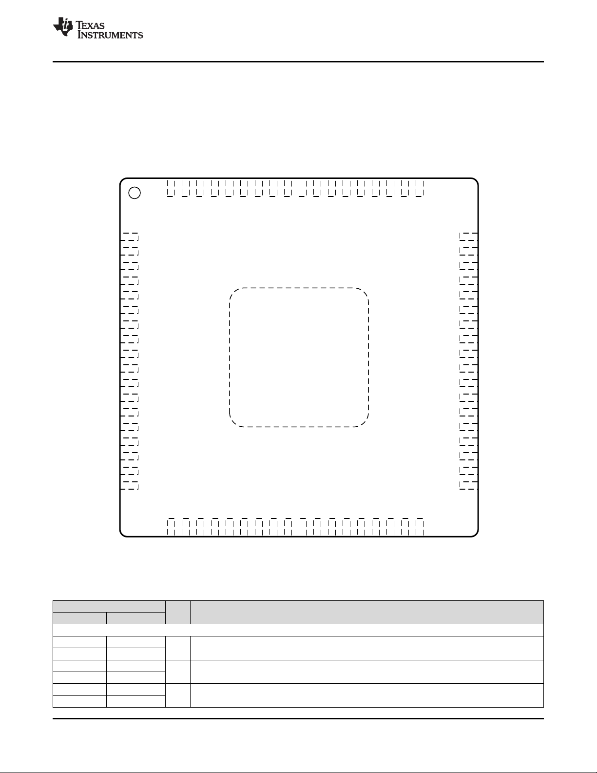
5 Pin Configuration and Functions
ADS58J64
SBAS807A –JANUARY 2017–REVISED JANUARY 2017
RMP Package
72-Pin VQFN
Top View
NAME NO.
INPUT, REFERENCE
INAM 41
INAP 42
INBM 37
INBP 36
INCM 18
INCP 19
PIN
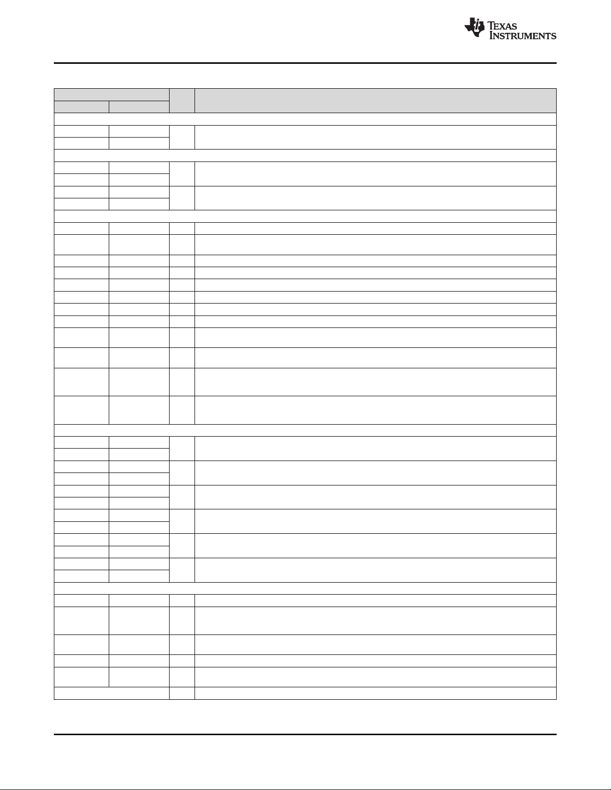
Pin Functions
I/O DESCRIPTION
I Differential analog input pin for channel A, internal bias via a 2-kΩ resistor to V
I Differential analog input pin for channel B, internal bias via a 2-kΩ resistor to V
I Differential analog input pin for channel C, internal bias via a 2-kΩ resistor to V
CM
CM
CM
Product Folder Links: ADS58J64
Submit Documentation FeedbackCopyright © 2017, Texas Instruments Incorporated
3
ADS58J64
SBAS807A –JANUARY 2017–REVISED JANUARY 2017
Pin Functions (continued)
PIN
NAME NO.
INPUT, REFERENCE (continued)
INDM 14
INDP 13
CLOCK, SYNC
CLKINM 28
CLKINP 27
SYSREFM 34
SYSREFP 33
CONTROL, SERIAL
NC 22, 23 — No connection
PDN 50 I/O
RES 49 — Reserved pin, connect to GND
RESET 48 I Hardware reset; active high. This pin has an internal 10-kΩ pulldown resistor.
SCLK 6 I Serial interface clock input. This pin has an internal 10-kΩ pulldown resistor.
SDIN 5 I Serial interface data input. This pin has an internal 10-kΩ pulldown resistor.
SDOUT 11 O 1.8-V logic serial interface data output
SEN 7 I Serial interface enable. This pin has an internal 10-kΩ pullup resistor to DVDD.
TRDYAB 54 O
TRDYCD 1 O
TRIGAB 53 I
TRIGCD 2 I
DATA INTERFACE
DAM 59
DAP 58
DBM 62
DBP 61
DCM 65
DCP 66
DDM 68
DDP 69
SYNCbABM 56
SYNCbABP 55
SYNCbCDM 71
SYNCbCDP 72
POWER SUPPLY
AGND 21, 26, 29, 32 I Analog ground
AVDD
AVDD19
DGND 3, 52, 60, 63, 67 I Digital ground
DVDD
Thermal pad — Connect to GND
9, 12, 15, 17, 20,
25, 30, 35, 38,
40, 43, 44, 46
10, 16, 24, 31,
39, 45
4, 8, 47,51, 57,
64, 70
I/O DESCRIPTION
I Differential analog input pin for channel D, internal bias via a 2-kΩ resistor to V
I Differential clock input pin for the ADC with internal 100-Ω differential termination, requires external ac coupling
I External SYSREF input, requires dc coupling and external termination
Power down. This pin can be configured via an SPI register setting. This pin has an internal 10-kΩ pulldown
resistor.
Trigger-ready output for burst mode for channels A and B. This pin can be configured via SPI to a TRDY signal for
all four channels in burst mode, and can be left open if not used.
Trigger-ready output for burst mode for channels C and D. This pin can be configured via SPI to a TRDY signal for
all four channels in burst mode, and can be left open if not used.
Manual burst mode trigger input for channels A and B. This pin can be configured via SPI to a manual trigger input
signal for all four channels in burst mode, and can be connected to GND if not used. This pin has an internal 10kΩ pulldown resistor.
Manual burst mode trigger input for channels C and D. This pin can be configured via SPI to a manual trigger
input signal for all four channels in burst mode, and can be connected to GND if not used. This pin has an internal
10-kΩ pulldown resistor.
O JESD204B serial data output pin for channel A
O JESD204B serial data output pin for channel B
O JESD204B serial data output pin for channel C
O JESD204B serial data output pin for channel D
Synchronization input pin for JESD204B port channels A and B. This pin can be configured via SPI to a SYNCb
I
signal for all four channels. This pin has an internal differential termination of 100 Ω.
Synchronization input pin for JESD204B port channels C and D. This pin can be configured via SPI to a SYNCb
I
signal for all four channels. This pin has an internal differential termination of 100 Ω..
I Analog 1.15-V power supply
I Analog 1.9-V supply for analog buffer
I Digital 1.15-V power supply
www.ti.com
CM
4
Submit Documentation Feedback Copyright © 2017, Texas Instruments Incorporated
Product Folder Links: ADS58J64
ADS58J64
www.ti.com
SBAS807A –JANUARY 2017–REVISED JANUARY 2017
6 Specifications
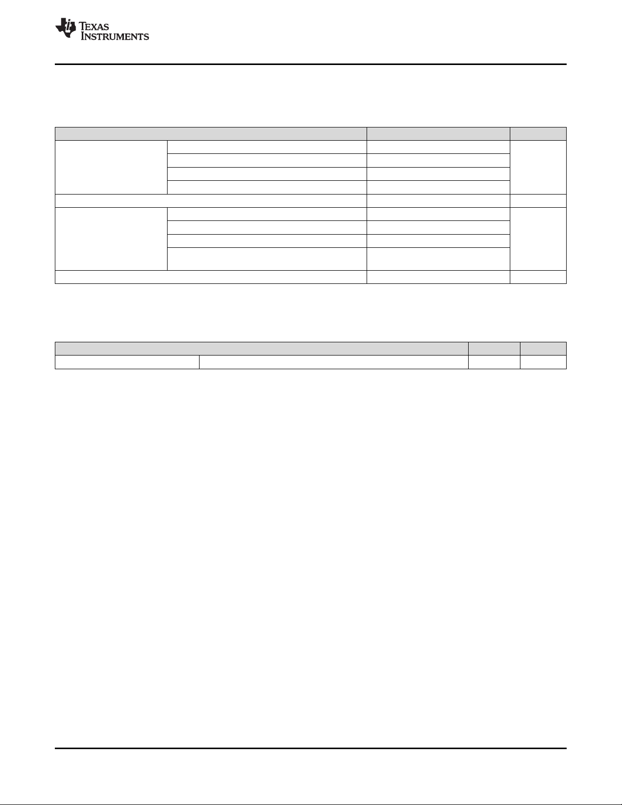
6.1 Absolute Maximum Ratings
over operating free-air temperature range (unless otherwise noted)
AVDD19 –0.3 2.1
Supply voltage
Voltage between AGND and DGND –0.3 0.3 V
Voltage applied to input pins
Storage temperature, T
(1) Stresses beyond those listed under Absolute Maximum Ratings may cause permanent damage to the device. These are stress ratings
only, which do not imply functional operation of the device at these or any other conditions beyond those indicated under Recommended
Operating Conditions. Exposure to absolute-maximum-rated conditions for extended periods may affect device reliability.
AVDD –0.3 1.4
DVDD –0.3 1.4
IOVDD –0.2 1.4
INAP, INBP, INAM, INBM, INCP, INDP, INCM, INDM –0.3 2.1
CLKINP, CLKINM –0.3 AVDD + 0.3
SYSREFP, SYSREFM, TRIGAB, TRIGCD –0.3 AVDD + 0.3
SCLK, SEN, SDIN, RESET, SYNCbABP,
SYNCbABM, SYNCbCDP, SYNCbCDM, PDN
stg
6.2 ESD Ratings
V
(ESD)
(1) JEDEC document JEP155 states that 500-V HBM allows safe manufacturing with a standard ESD control process.
Electrostatic discharge Human-body model (HBM), per ANSI/ESDA/JEDEC JS-001
(1)
MIN MAX UNIT
V
V
–0.2 AVDD19 + 0.3
–65 150 °C
VALUE UNIT
(1)
±2000 V
Product Folder Links: ADS58J64
Submit Documentation FeedbackCopyright © 2017, Texas Instruments Incorporated
5
ADS58J64
SBAS807A –JANUARY 2017–REVISED JANUARY 2017
www.ti.com
6.3 Recommended Operating Conditions
over operating free-air temperature range (unless otherwise noted)
MIN NOM MAX UNIT
AVDD19 1.8 1.9 2
Supply voltage range
Analog inputs
Clock inputs
Temperature
(1) Assumes system thermal design meets the TJspecification.
(2) Prolonged use above this junction temperature can increase the device failure-in-time (FIT) rate.
(3) The recommended maximum temperature at the PCB footprint thermal pad assumes the junction-to-package bottom thermal resistance,
R
consumption is 2.5 W.
= 0.2°C/W, the thermal resistance of the device thermal pad connection to the PCB footprint is negligible, and the device power
θJC(bot)
AVDD 1.1 1.15 1.2
DVDD 1.1 1.15 1.2
V
IOVDD 1.1 1.15 1.2
Differential input voltage range 1.1 V
PP
Input common-mode voltage (VCM) 1.3 V
Input clock frequency, device clock frequency 400 1000 MHz
Sine wave, ac-coupled 1.5
Input clock amplitude differential
(V
– V
CLKM
)
CLKP
LVPECL, ac-coupled 1.6
LVDS, ac-coupled 0.7
V
PP
Input device clock duty cycle, default after reset 45% 50% 55%
104.5
(1)
(2)
ºC
(3)
Operating free-air, T
Operating junction, T
A
J
Specified maximum, measured at the device footprint thermal
pad on the printed circuit board, T
P-MAX
–40 100
105 125
6.4 Thermal Information
ADS58J64
THERMAL METRIC
R
θJA
R
θJC(top)
R
θJB
ψ
JT
ψ
JB
R
θJC(bot)
Junction-to-ambient thermal resistance
Junction-to-case (top) thermal resistance
Junction-to-board thermal resistance
Junction-to-top characterization parameter
Junction-to-board characterization parameter
Junction-to-case (bottom) thermal resistance
(1) For more information about traditional and new thermal metrics, see the Semiconductor and IC Package Thermal Metrics application
report.
(2) The junction-to-ambient thermal resistance under natural convection is obtained in a simulation on a JEDEC-standard, high-K board, as
specified in JESD51-7, in an environment described in JESD51-2a.
(3) The junction-to-case (top) thermal resistance is obtained by simulating a cold plate test on the package top. No specific JEDEC-
standard test exists, but a close description can be found in the ANSI SEMI standard G30-88.
(4) The junction-to-board thermal resistance is obtained by simulating in an environment with a ring cold plate fixture to control the PCB
temperature, as described in JESD51-8.
(5) The junction-to-top characterization parameter, ψJT, estimates the junction temperature of a device in a real system and is extracted
from the simulation data for obtaining θJA, using a procedure described in JESD51-2a (sections 6 and 7).
(6) The junction-to-board characterization parameter, ψJB, estimates the junction temperature of a device in a real system and is extracted
from the simulation data for obtaining θJA , using a procedure described in JESD51-2a (sections 6 and 7).
(1)
UNITRMP (VQFNP)
72 PINS
(2)
(3)
(3)
(4)
(5)
(6)
22.3 °C/W
5.1 °C/W
2.4 °C/W
0.1 °C/W
2.3 °C/W
0.2 °C/W
6
Submit Documentation Feedback Copyright © 2017, Texas Instruments Incorporated
Product Folder Links: ADS58J64
ADS58J64
www.ti.com
SBAS807A –JANUARY 2017–REVISED JANUARY 2017
6.5 Electrical Characteristics
typical values are at TA= 25°C, full temperature range is from T
mode 8: 2x decimation with burst mode output, 50% clock duty cycle, AVDD19 = 1.9 V, AVDD = DVDD = 1.15 V, –1-dBFS
differential input, and fIN= 190 MHz (unless otherwise noted)
PARAMETER TEST CONDITIONS MIN TYP MAX UNIT
GENERAL
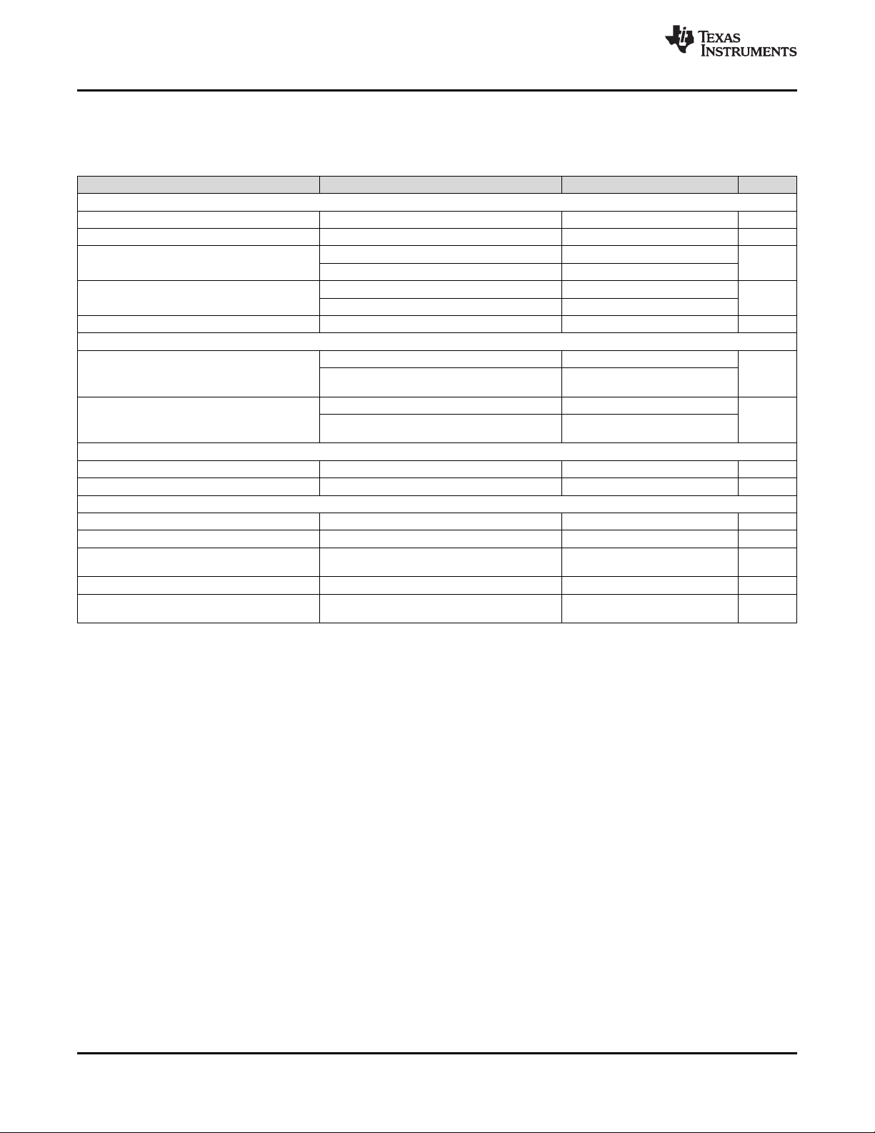
ADC sampling rate 1 GSPS
Resolution 14 Bits
POWER SUPPLY
AVDD19 1.9-V analog supply 1.85 1.9 1.95 V
AVDD 1.15-V analog supply 1.1 1.15 1.2 V
DVDD 1.15-V digital supply 1.1 1.15 1.2 V
I
AVDD19
I
AVDD
I
DVDD
Pdis Total power dissipation
ANALOG INPUTS
ISOLATION
1.9-V analog supply current 100-MHz, full-scale input on all four channels 618 mA
1.15-V analog supply current 100-MHz, full-scale input on all four channels 415 mA
Mode 8, 100 MHz, full-scale input on all four
channels
Mode 3, 100 MHz, full-scale input on all four
1.15-V digital supply current
channels
Mode 0 and 2, 100 MHz, full-scale input on all four
channels
Mode 1, 4, 6, and 7, 100 MHz, full-scale input on
all four channels
Mode 8, 100 MHz, full-scale input on all four
channels
Mode 3, 100 MHz, full-scale input on all four
channels
Mode 0 and 2, 100 MHz, full-scale input on all four
channels
Mode 1, 4, 6, and 7, 100 MHz, full-scale input on
all four channels
Global power-down power
dissipation
Full-scale input on all four channels 120 mW
Differential input full-scale
voltage
Input common-mode voltage 1.3 V
Differential input resistance At fIN= dc 4 kΩ
Differential input capacitance 2.5 pF
Analog input bandwidth (3 dB) 1000 MHz
fIN= 10 MHz 75
Crosstalk
(1)
isolation between
near channels
(channels A and B are near to
each other, channels C and D
are near to each other)
fIN= 100 MHz 75
fIN= 170 MHz 74
fIN= 270 MHz 72
fIN= 370 MHz 71
fIN= 470 MHz 70
fIN= 10 MHz 110
Crosstalk
(1)
isolation between
far channels
(channels A and B are far from
channels C and D)
fIN= 100 MHz 110
fIN= 170 MHz 110
fIN= 270 MHz 110
fIN= 370 MHz 110
fIN= 470 MHz 110
= –40°C to T
MIN
= +100°C, input clock frequency = 1 GHz,
MAX
629
730
674
703
2.37
2.49
2.42
2.46
1.1 V
mA
W
dBFS
dBFS
PP
(1) Crosstalk is measured with a –1-dBFS input signal on aggressor channel and no input on the victim channel.
Submit Documentation FeedbackCopyright © 2017, Texas Instruments Incorporated
Product Folder Links: ADS58J64
7
ADS58J64
SBAS807A –JANUARY 2017–REVISED JANUARY 2017
Electrical Characteristics (continued)
www.ti.com
typical values are at TA= 25°C, full temperature range is from T
= –40°C to T
MIN
= +100°C, input clock frequency = 1 GHz,
MAX
mode 8: 2x decimation with burst mode output, 50% clock duty cycle, AVDD19 = 1.9 V, AVDD = DVDD = 1.15 V, –1-dBFS
differential input, and fIN= 190 MHz (unless otherwise noted)
PARAMETER TEST CONDITIONS MIN TYP MAX UNIT
CLOCK INPUT
Internal clock biasing
CLKINP and CLKINM pins are connected to the
internal biasing voltage through a 5-kΩ resistor
0.7 V
6.6 AC Performance
typical values are at TA= 25°C, full temperature range is from T
mode 8: 2x decimation with burst mode output, 50% clock duty cycle, AVDD19 = 1.9 V, AVDD = DVDD = 1.15 V, –1-dBFS
differential input, and fIN= 190 MHz (unless otherwise noted)
PARAMETER TEST CONDITIONS
fIN= 10 MHz, AIN= –1 dBFS 69.9 72.2
fIN= 70 MHz, AIN= –1 dBFS 69.6 71.8
fIN= 190 MHz, AIN= –1 dBFS 69.2 71.8
SNR Signal-to-noise ratio
NSD Noise spectral density
Spurious-free dynamic
(1)
SFDR
SINAD
range
Signal-to-noise and
distortion ratio
(1) Harmonic distortion performance can be significantly improved by using the frequency planning explained in the Frequency Planning
section.
fIN= 190 MHz, AIN= –3 dBFS 66.5 69.6 71
fIN= 300 MHz, AIN= –3 dBFS 69.3 71.7
fIN= 370 MHz, AIN= –3 dBFS 68.7 71.3
fIN= 470 MHz, AIN= –3 dBFS 68.4 69.8
fIN= 10 MHz, AIN= –1 dBFS –153.9 –153.2
fIN= 70 MHz, AIN= –1 dBFS –153.6 –152.8
fIN= 190 MHz, AIN= –1 dBFS –153.2 –152.7
fIN= 190 MHz, AIN= –3 dBFS –150.5 –153.6 –153.2
fIN= 300 MHz, AIN= –3 dBFS –152.8 –152.7
fIN= 370 MHz, AIN= –3 dBFS –152.5 –152.2
fIN= 470 MHz, AIN= –3 dBFS –151.5 –151
fIN= 10 MHz, AIN= –1 dBFS 83 83
fIN= 70 MHz, AIN= –1 dBFS 81 100
fIN= 190 MHz, AIN= –1 dBFS 87 100
fIN= 190 MHz, AIN= –3 dBFS 78 88 98
fIN= 300 MHz, AIN= –3 dBFS 79 98
fIN= 370 MHz, AIN= –3 dBFS,
input clock frequency = 983.04 MHz
fIN= 470 MHz, AIN= –3 dBFS 78 76
fIN= 10 MHz, AIN= –1 dBFS 68.5 70.6
fIN= 70 MHz, AIN= –1 dBFS 68.5 70.6
fIN= 190 MHz, AIN= –1 dBFS 68.2 72.2
fIN= 190 MHz, AIN= –3 dBFS 68.5 73
fIN= 300 MHz, AIN= –3 dBFS 68.9 72.3
fIN= 370 MHz, AIN= –3 dBFS 68 68.2
fIN= 470 MHz, AIN= –3 dBFS 68 69
= –40°C to T
MIN
= +100°C, input clock frequency = 1 GHz,
MAX
MIN TYP MAX MIN TYP MAX
14-BIT BURST MODE
(DDC Mode 8)
82 70
DECIMATE-BY-4
(DDC Mode 2)
UNIT
dBFS
dBFS/Hz
dBc
dBFS
8
Submit Documentation Feedback Copyright © 2017, Texas Instruments Incorporated
Product Folder Links: ADS58J64
www.ti.com
AC Performance (continued)
ADS58J64
SBAS807A –JANUARY 2017–REVISED JANUARY 2017
typical values are at TA= 25°C, full temperature range is from T
= –40°C to T
MIN
= +100°C, input clock frequency = 1 GHz,
MAX
mode 8: 2x decimation with burst mode output, 50% clock duty cycle, AVDD19 = 1.9 V, AVDD = DVDD = 1.15 V, –1-dBFS
differential input, and fIN= 190 MHz (unless otherwise noted)
MIN TYP MAX MIN TYP MAX
(1)
HD2
(1)
HD3
Non
HD2, HD3
(1)
THD
IMD3
PARAMETER TEST CONDITIONS
fIN= 10 MHz, AIN= –1 dBFS –83 –90
fIN= 70 MHz, AIN= –1 dBFS –82 –100
fIN= 190 MHz, AIN= –1 dBFS –85 –98
Second-order harmonic
distortion
Third-order harmonic
distortion
Spurious-free dynamic
range (excluding HD2,
HD3)
Total harmonic distortion
Two-tone, third-order
intermodulation distortion
fIN= 190 MHz, AIN= –3 dBFS –78 –86 –100
fIN= 300 MHz, AIN= –3 dBFS –82 –100
fIN= 370 MHz, AIN= –3 dBFS
input clock frequency = 983.04 MHz
fIN= 470 MHz, AIN= –3 dBFS –100 –94
fIN= 10 MHz, AIN= –1 dBFS –83 –85
fIN= 70 MHz, AIN= –1 dBFS –81 –100
fIN= 190 MHz, AIN= –1 dBFS –92 –100
fIN= 190 MHz, AIN= –3 dBFS –78 –92 –100
fIN= 300 MHz, AIN= –3 dBFS –90 –100
fIN= 370 MHz, AIN= –3 dBFS –90 –100
fIN= 470 MHz, AIN= –3 dBFS –80 –79
fIN= 10 MHz, AIN= –1 dBFS 95 –100
fIN= 70 MHz, AIN= –1 dBFS 95 –92
fIN= 190 MHz, AIN= –1 dBFS 95 –100
fIN= 190 MHz, AIN= –3 dBFS 87 95 –98
fIN= 300 MHz, AIN= –3 dBFS 95 –100
fIN= 370 MHz, AIN= –3 dBFS 95 –100
fIN= 470 MHz, AIN= –3 dBFS 93 –100
fIN= 10 MHz, AIN= –1 dBFS –81 –83
fIN= 70 MHz, AIN= –1 dBFS –79 –100
fIN= 190 MHz, AIN= –1 dBFS –83 –100
fIN= 190 MHz, AIN= –3 dBFS –85 –100
fIN= 300 MHz, AIN= –3 dBFS –81 –100
fIN= 370 MHz, AIN= –3 dBFS –76 –68
fIN= 470 MHz, AIN= –3 dBFS –82 –80
f1= 185 MHz, f2= 190 MHz,
AIN= –10 dBFS
f1= 365 MHz, f2= 370 MHz,
AIN= –10 dBFS
f1= 465 MHz, f2= 470 MHz,
AIN= –10 dBFS
14-BIT BURST MODE
(DDC Mode 8)
–82 –69
–90 –87
–90 –94
–85 –85
DECIMATE-BY-4
(DDC Mode 2)
UNIT
dBc
dBc
dBFS
dBc
dBFS
Product Folder Links: ADS58J64
Submit Documentation FeedbackCopyright © 2017, Texas Instruments Incorporated
9
ADS58J64
SBAS807A –JANUARY 2017–REVISED JANUARY 2017
www.ti.com
6.7 Digital Characteristics
typical values are at TA= 25°C, full temperature range is from T
mode 8: 2x decimation with burst mode output, 50% clock duty cycle, AVDD19 = 1.9 V, AVDD = DVDD = 1.15 V, –1-dBFS
differential input, and fIN= 190 MHz (unless otherwise noted)
PARAMETER TEST CONDITIONS MIN TYP MAX UNIT
DIGITAL INPUTS (RESET, SCLK, SEN, SDIN, PDN, TRIGAB, TRIGCD)
V
IH
V
IL
I
IH
I
IL
High-level input voltage All digital inputs support 1.2-V and 1.8-V logic levels 0.8 V
Low-level input voltage All digital inputs support 1.2-V and 1.8-V logic levels 0.4 V
High-level input current
Low-level input current
SEN 0
RESET, SCLK, SDIN, PDN, TRIGAB, TRIGCD 50
SEN 50
RESET, SCLK, SDIN, PDN, TRIGAB, TRIGCD 0
Input capacitance 4 pF
DIGITAL INPUTS
SYSREFP, SYSREFM 0.35 0.45 0.55
V
D
Differential input voltage
SYNCbABM, SYNCbABP, SYNCbCDM,
SYNCbCDP
SYSREFP, SYSREFM 0.9 1.2 1.4
V
(CM_DIG)
Common-mode voltage for SYSREF
SYNCbABM, SYNCbABP, SYNCbCDM,
SYNCbCDP
DIGITAL OUTPUTS (SDOUT, TRDYAB, TRDYCD)
V
OH
V
OL
DIGITAL OUTPUTS (JESD204B Interface: DxP, DxM)
V
OD
V
OC
z
os
High-level output voltage 100-µA current AVDD19 – 0.2 V
Low-level output voltage 100-µA current 0.2 V
(2)
Output differential voltage With default swing setting 700 mV
Output common-mode voltage 450 mV
Transmitter short-circuit current
Transmitter pins shorted to any voltage between
–0.25 V and 1.45 V
Single-ended output impedance 50 Ω
Output capacitance
Output capacitance inside the device,
from either output to ground
(1) The RESET, SCLK, SDIN, and PDN pins have a 20-kΩ (typical) internal pulldown resistor to ground, and the SEN pin has a 20-kΩ
(typical) pullup resistor to IOVDD.
(2) 50-Ω, single-ended external termination to IOVDD.
(1)
= –40°C to T
MIN
= +100°C, input clock frequency = 1 GHz,
MAX
0.35 1.3
1.2
–100 100 mA
2 pF
µA
µA
V
V
PP
10
Submit Documentation Feedback Copyright © 2017, Texas Instruments Incorporated
Product Folder Links: ADS58J64
CLKINM
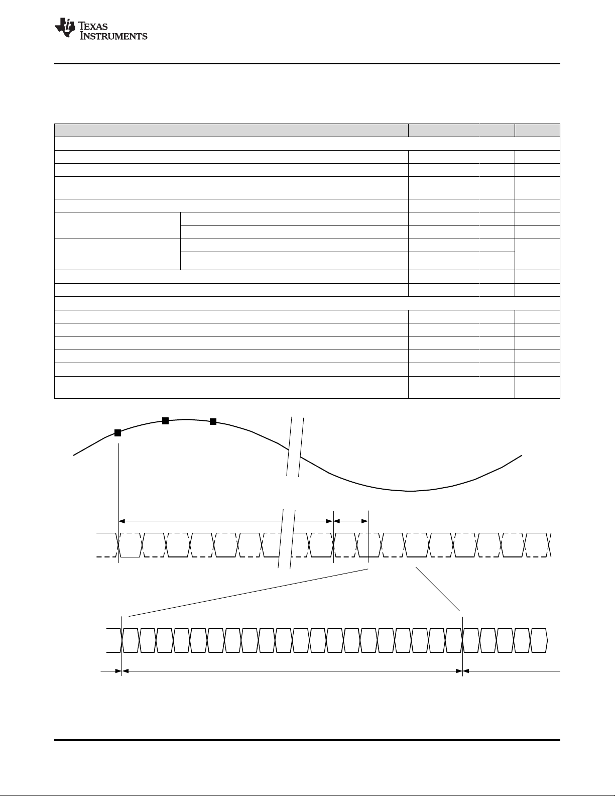
Data Latency: 116 Clock Cycles
N
t
PD
CLKINP
DAP, DAM
DBP, DBM
DCP, DCM
DDP, DDM
Sample N Sample N+1Sample N-1
D20 D1 D20
Sample
N+1
N+2
ADS58J64
www.ti.com
SBAS807A –JANUARY 2017–REVISED JANUARY 2017
6.8 Timing Characteristics
typical values are at TA= 25°C, full temperature range is from T
mode 8: 2x decimation with burst mode output, 50% clock duty cycle, AVDD19 = 1.9 V, AVDD = DVDD = 1.15 V, –1-dBFS
differential input, and fIN= 190 MHz (unless otherwise noted)
SAMPLE TIMING CHARACTERISTICS
Aperture delay 0.55 0.92 ns
Aperture delay matching between two channels on the same device ±100 ps
Aperture delay matching between two devices at the same temperature and supply
voltage
Aperture jitter 100 fSrms
Wake-up time
Data latency: ADC
sample to digital
output
t
SU_SYSREF
t
H_SYSREF
Setup time for SYSREF, referenced to input clock rising edge 350 900 ps
Hold time for SYSREF, referenced to input clock rising edge 100 ps
JESD OUTPUT INTERFACE TIMING CHARACTERISTICS
Unit interval 100 ps
Serial output data rate 10 Gbps
Total jitter for BER of 1E-15 and lane rate = 10 Gbps 24 ps
Random jitter for BER of 1E-15 and lane rate = 10 Gbps 0.95 ps rms
Deterministic jitter for BER of 1E-15 and lane rate = 10 Gbps 8.8 ps, pk-pk
tR, t
F
Data rise time, data fall time: rise and fall times measured from 20% to 80%,
differential output waveform, 2.5 Gbps ≤ bit rate ≤ 10 Gbps
Global power-down 10 ms
Pin power-down (fast power-down) 5 µs
Burst mode 116
DDC mode 0 204
= –40°C to T
MIN
= +100°C, input clock frequency = 1 GHz,
MAX
MIN TYP MAX UNITS
±100 ps
Input clock
35 ps
cycles
Figure 1. Latency Timing Diagram in Burst Mode
Product Folder Links: ADS58J64
Submit Documentation FeedbackCopyright © 2017, Texas Instruments Incorporated
11
Input Frequency (MHz)
Amplitude (dBFS)
0 50 100 150 200 250
-140
-120
-100
-80
-60
-40
-20
0
D005
Input Frequency (dBFS)
Amplitude (dBFS)
0 50 100 150 200 250
-140
-120
-100
-80
-60
-40
-20
0
D006
Input Frequency (MHz)
Amplitude (dBFS)
0 50 100 150 200 250
-140
-120
-100
-80
-60
-40
-20
0
D003
Input Frequency (MHz)
Amplitude (dBFS)
0 50 100 150 200 250
-140
-120
-100
-80
-60
-40
-20
0
D004
Input Frequency (MHz)
Amplitude (dBFS)
0 50 100 150 200 250
-140
-120
-100
-80
-60
-40
-20
0
D001
Input Frequency (MHz)
Amplitude (dBFS)
0 50 100 150 200 250
-140
-120
-100
-80
-60
-40
-20
0
D002
ADS58J64
SBAS807A –JANUARY 2017–REVISED JANUARY 2017
www.ti.com
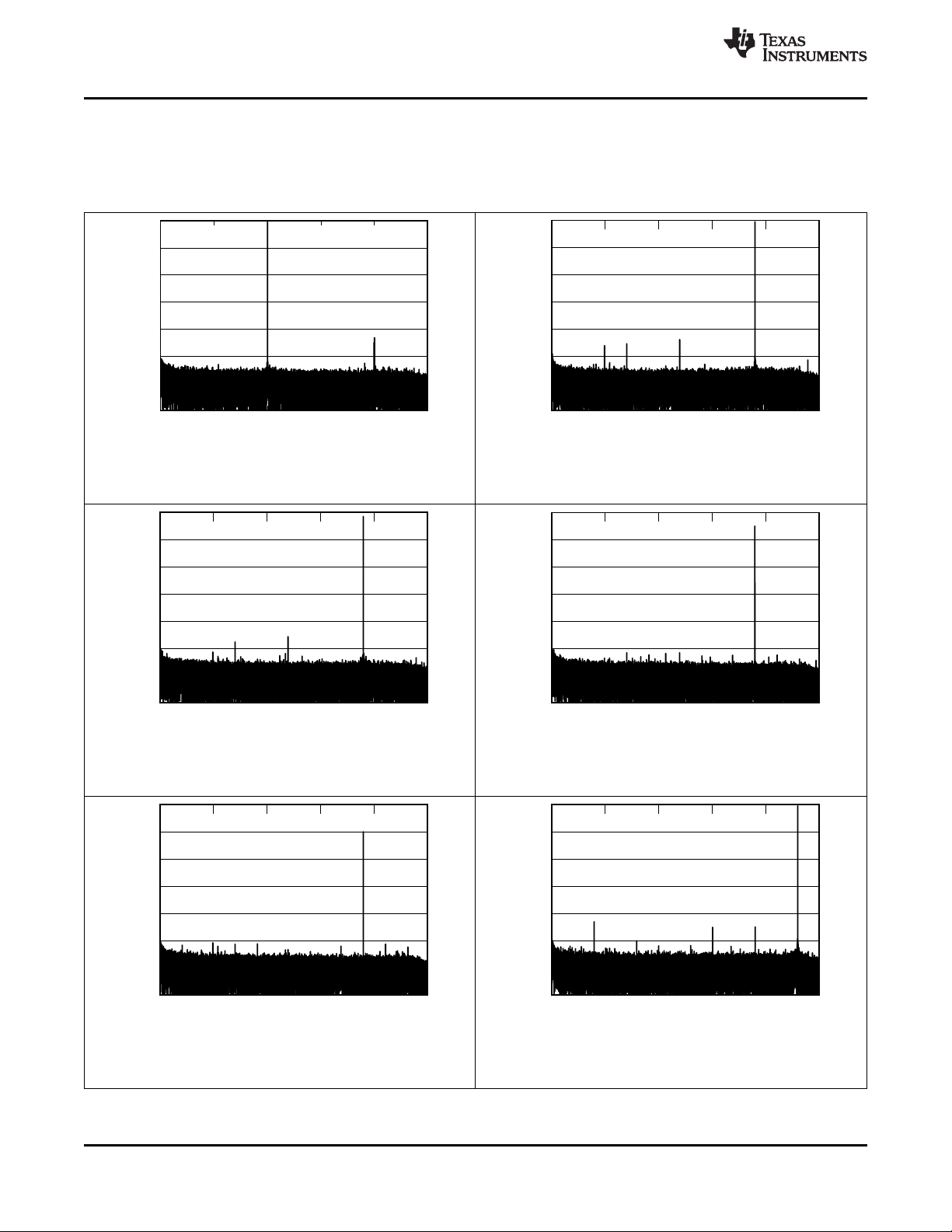
6.9 Typical Characteristics: 14-Bit Burst Mode
typical values are at TA= 25°C, full temperature range is from T
1 GSPS, mode 8: 2x decimation with burst mode output, 50% clock duty cycle, AVDD19 = 1.9 V, AVDD = DVDD = 1.15 V,
–1-dBFS differential input, and fIN= 190 MHz (unless otherwise noted)
= –40°C to T
MIN
= +100°C, device sampling frequency =
MAX
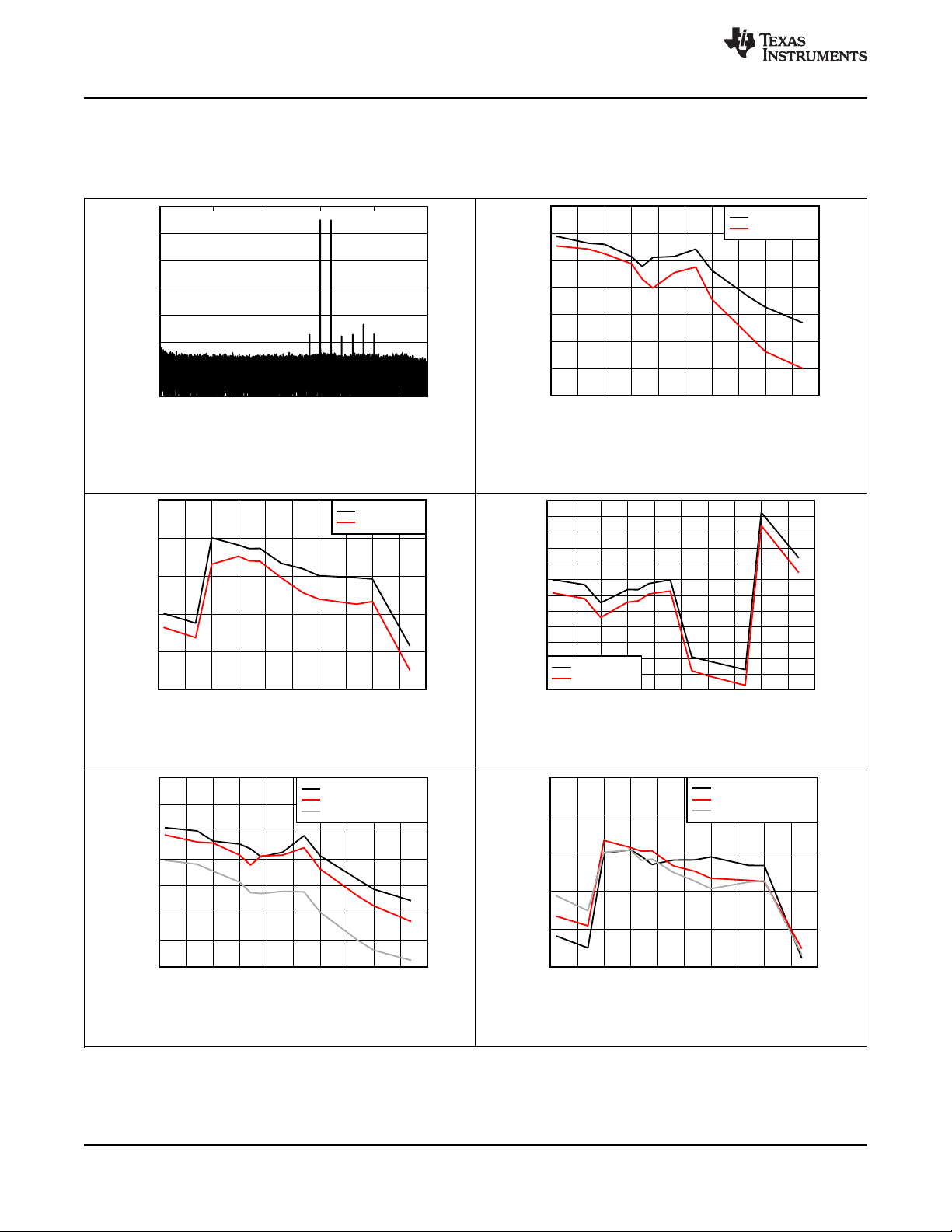
fIN= 100 MHz, AIN= –1 dBFS, SNR = 69.57 dBFS,
SFDR = 85.23 dBc, SFDR = 102.09 dBc (non 23)
Figure 2. FFT for 100-MHz Input Signal
fIN= 190 MHz, AIN= –3 dBFS, SNR = 69.60 dBFS,
SFDR = 88.45 dBc, SFDR = 99.78 dBc (non 23)
Figure 4. FFT for 190-MHz Input Signal
fIN= 190 MHz, AIN= –1 dBFS, SNR = 69.23 dBFS,
SFDR = 86.83 dBc, SFDR = 91.23 dBc (non 23)
Figure 3. FFT for 190-MHz Input Signal
fIN= 190 MHz, AIN= –10 dBFS, SNR = 70.05 dBFS,
SFDR = 93.27 dBc, SFDR = 97.26 dBc (non 23)
Figure 5. FFT for 190-MHz Input Signal
fIN= 190 MHz, AIN= –20 dBFS, SNR = 70.23 dBFS,
SFDR = 81.71 dBc, SFDR = 81.71 dBc (non 23)
12
Submit Documentation Feedback Copyright © 2017, Texas Instruments Incorporated
Figure 6. FFT for 190-MHz Input Signal
fIN= 230 MHz, AIN= –1 dBFS, SNR = 69.17 dBFS,
SFDR = 85.29 dBc, SFDR = 89.30 dBc (non 23)
Figure 7. FFT for 230-MHz Input Signal
Product Folder Links: ADS58J64
Input Frequency (MHz)
Amplitude (dBFS)
0 50 100 150 200 250
-140
-120
-100
-80
-60
-40
-20
0
D011
Input Frequency (MHz)
Amplitude (dBFS)
0 50 100 150 200 250
-140
-120
-100
-80
-60
-40
-20
0
D012
Input Frequency (MHz)
Amplitude (dBFS)
0 50 100 150 200 250
-140
-120
-100
-80
-60
-40
-20
0
D009
Input Frequency (MHz)
Amplitude (dBFS)
0 50 100 150 200 250
-140
-120
-100
-80
-60
-40
-20
0
D010
Input Frequency (MHz)
Amplitude (dBFS)
0 50 100 150 200 250
-140
-120
-100
-80
-60
-40
-20
0
D007
Input Frequency (MHz)
Amplitude (dBFS)
0 50 100 150 200 250
-140
-120
-100
-80
-60
-40
-20
0
D008
www.ti.com
Typical Characteristics: 14-Bit Burst Mode (continued)
ADS58J64
SBAS807A –JANUARY 2017–REVISED JANUARY 2017
typical values are at TA= 25°C, full temperature range is from T
= –40°C to T
MIN
= +100°C, device sampling frequency =
MAX
1 GSPS, mode 8: 2x decimation with burst mode output, 50% clock duty cycle, AVDD19 = 1.9 V, AVDD = DVDD = 1.15 V,
–1-dBFS differential input, and fIN= 190 MHz (unless otherwise noted)
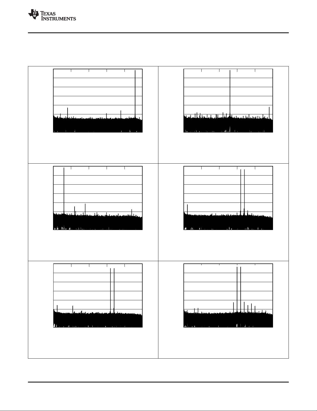
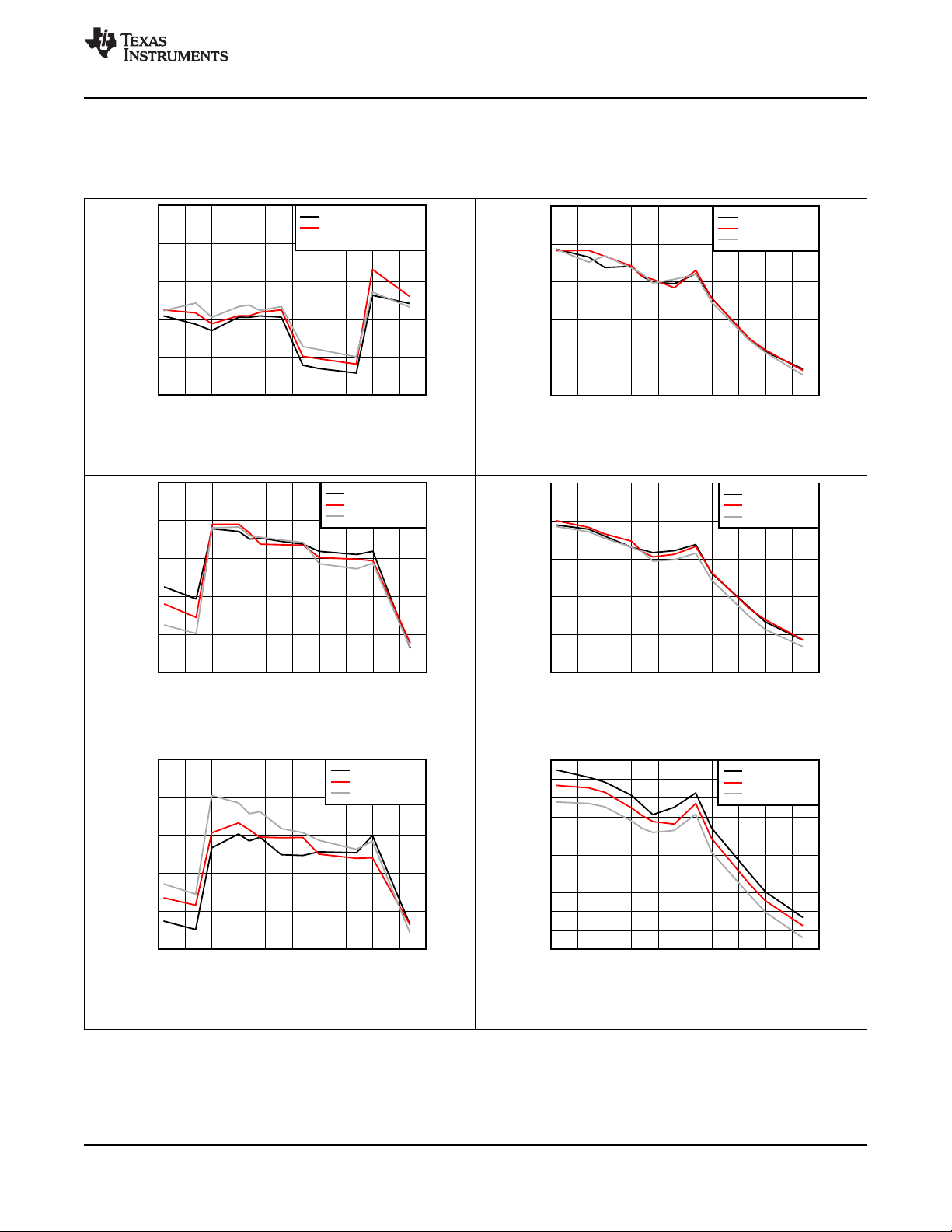
fIN= 270 MHz, AIN= –3 dBFS, SNR = 69.27 dBFS,
SFDR = 82.98 dBc, SFDR = 95.4 dBc (non 23)
Figure 8. FFT for 270-MHz Input Signal
fIN= 370 MHz, AIN= –3 dBFS, SNR = 68.36 dBFS,
SFDR = 81.37 dBc, SFDR = 97.28 dBc (non 23)
Figure 9. FFT for 370-MHz Input Signal
fIN= 470 MHz, AIN= –3 dBFS, SNR = 68.21 dBFS,
SFDR = 79.85 dBc, SFDR = 99.12 dBc (non 23)
Figure 10. FFT for 470-MHz Input Signal
f
= 160 MHz, f
IN1
Figure 12. FFT for Two-Tone Input Signal
IN2
each tone at –10 dBFS
= 170 MHz, IMD = 103.44 dBFS,
Product Folder Links: ADS58J64
f
= 160 MHz, f
IN1
= 170 MHz, IMD = 102.68 dBFS,
IN2
each tone at –7 dBFS
Figure 11. FFT for Two-Tone Input Signal
f
= 340 MHz, f
IN1
= 350 MHz, IMD = 84.34 dBFS,
IN2
each tone at –7 dBFS
Figure 13. FFT for Two-Tone Input Signal
Submit Documentation FeedbackCopyright © 2017, Texas Instruments Incorporated
13
Input Frequency (MHz)
Signal-to-Noise Ratio (dBFS)
0 50 100 150 200 250 300 350 400 450 500
67.5
68
68.5
69
69.5
70
70.5
71
D017
Temperature = -40 qC
Temperature = 25 qC
Temperature = 105 qC
Input Frequency (MHz)
Third-Order Harmonic Distortion (dBc)
0 50 100 150 200 250 300 350 400 450 500
76
82
88
94
100
106
D018
Temperature = -40 qC
Temperature = 25 qC
Temperature = 105 qC
Input Frequency (MHz)
Third-Order Harmonic Distortion (dBc)
0 50 100 150 200 250 300 350 400 450 500
72
78
84
90
96
102
D015
AIN = -3 dBFS
AIN = -1 dBFS
Input Frequency (MHz)
Second-Order Harmonic Distortion (dBc)
0 50 100 150 200 250 300 350 400 450 500
74
76
78
80
82
84
86
88
90
92
94
96
98
D016
AIN = -3 dBFS
AIN = -1 dBFS
Input Frequency (MHz)
Amplitude (dBFS)
0 50 100 150 200 250
-140
-120
-100
-80
-60
-40
-20
0
D013
Input Frequency (MHz)
Signal-to-Noise Ratio (dBFS)
0 50 100 150 200 250 300 350 400 450 500
67
67.5
68
68.5
69
69.5
70
70.5
D014
AIN = -3 dBFS
AIN = -1 dBFS
ADS58J64
SBAS807A –JANUARY 2017–REVISED JANUARY 2017
Typical Characteristics: 14-Bit Burst Mode (continued)
www.ti.com
typical values are at TA= 25°C, full temperature range is from T
= –40°C to T
MIN
= +100°C, device sampling frequency =
MAX
1 GSPS, mode 8: 2x decimation with burst mode output, 50% clock duty cycle, AVDD19 = 1.9 V, AVDD = DVDD = 1.15 V,
–1-dBFS differential input, and fIN= 190 MHz (unless otherwise noted)
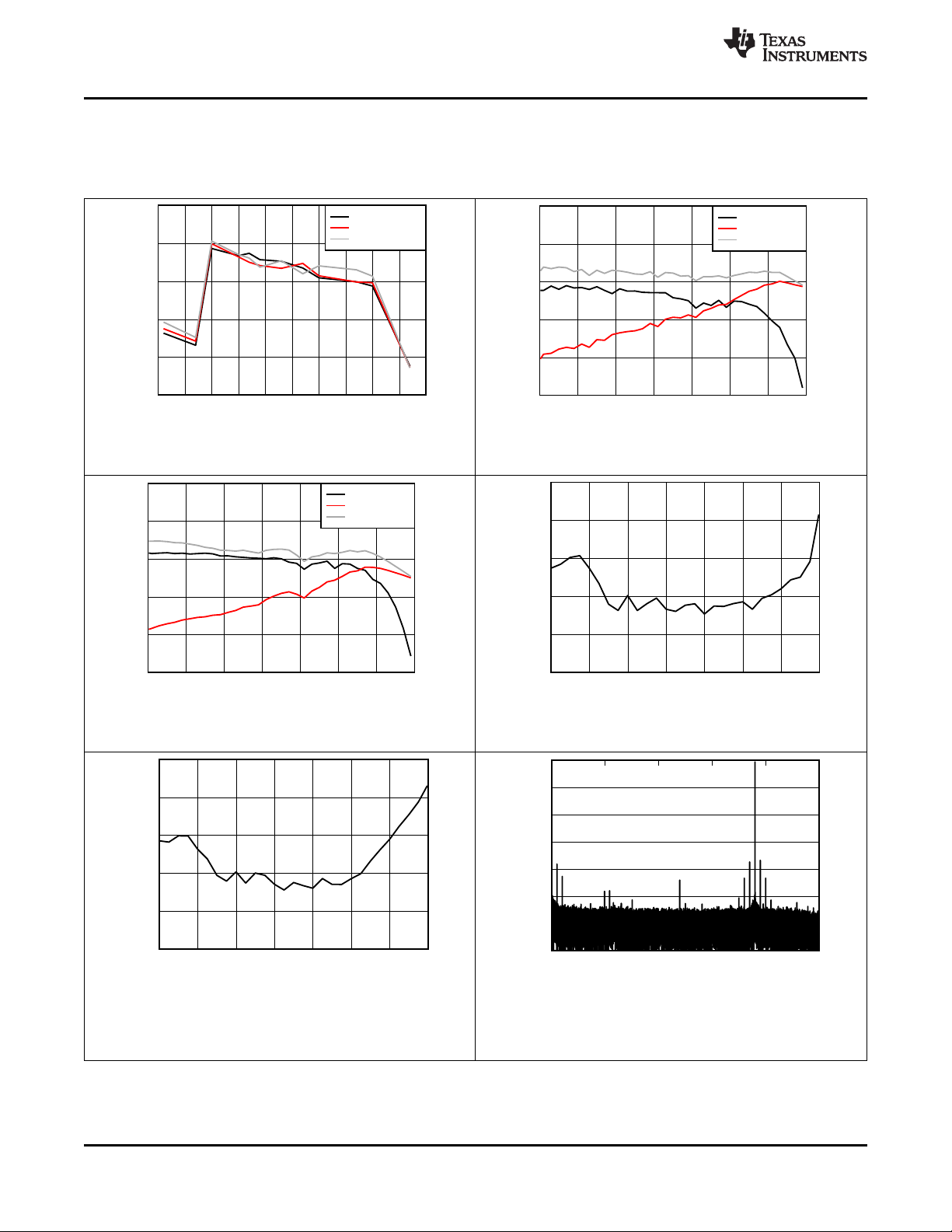
f
= 340 MHz, f
IN1
Figure 14. FFT for Two-Tone Input Signal
= 350 MHz, IMD = 95.08 dBFS,
IN2
each tone at –10 dBFS
Figure 15. SNR vs Input Frequency
Figure 16. HD3 vs Input Frequency Figure 17. HD2 vs Input Frequency
14
Figure 18. SNR vs Input Frequency and Temperature Figure 19. HD3 vs Input Frequency and Temperature
Submit Documentation Feedback Copyright © 2017, Texas Instruments Incorporated
Product Folder Links: ADS58J64
Input Frequency (MHz)
Third-Order Harmonic Distortion (dBc)
0 50 100 150 200 250 300 350 400 450 500
75
81
87
93
99
105
D023
AVDD = 1.1 V
AVDD = 1.15 V
AVDD = 1.2 V
Input Frequency (MHz)
Signal-to-Noise Ratio (dBFS)
0 50 100 150 200 250 300 350 400 450 500
68.2
68.4
68.6
68.8
69
69.2
69.4
69.6
69.8
70
70.2
D024
DVDD = 1.1 V
DVDD = 1.15 V
DVDD = 1.2 V
Input Frequency (MHz)
Third-Order Harmonic Distortion (dBc)
0 50 100 150 200 250 300 350 400 450 500
75
80
85
90
95
100
D021
AVDD19 = 1.8 V
AVDD19 = 1.9 V
AVDD19 = 2 V
Input Frequency (MHz)
Signal-to-Noise Ratio (dBFS)
0 50 100 150 200 250 300 350 400 450 500
68
68.5
69
69.5
70
70.5
D022
AVDD = 1.1 V
AVDD = 1.15 V
AVDD = 1.2 V
Input Frequency (MHz)
Second-Order Harmonic Distortion (dBc)
0 50 100 150 200 250 300 350 400 450 500
70
78
86
94
102
110
D019
Temperature = -40 qC
Temperature = 25 qC
Temperature = 105 qC
Input Frequency (MHz)
Signal-to-Noise Ratio (dBFS)
0 50 100 150 200 250 300 350 400 450 500
68
68.5
69
69.5
70
70.5
D020
AVDD19 = 1.8 V
AVDD19 = 1.9 V
AVDD19 = 2 V
www.ti.com
Typical Characteristics: 14-Bit Burst Mode (continued)
ADS58J64
SBAS807A –JANUARY 2017–REVISED JANUARY 2017
typical values are at TA= 25°C, full temperature range is from T
= –40°C to T
MIN
= +100°C, device sampling frequency =
MAX
1 GSPS, mode 8: 2x decimation with burst mode output, 50% clock duty cycle, AVDD19 = 1.9 V, AVDD = DVDD = 1.15 V,
–1-dBFS differential input, and fIN= 190 MHz (unless otherwise noted)
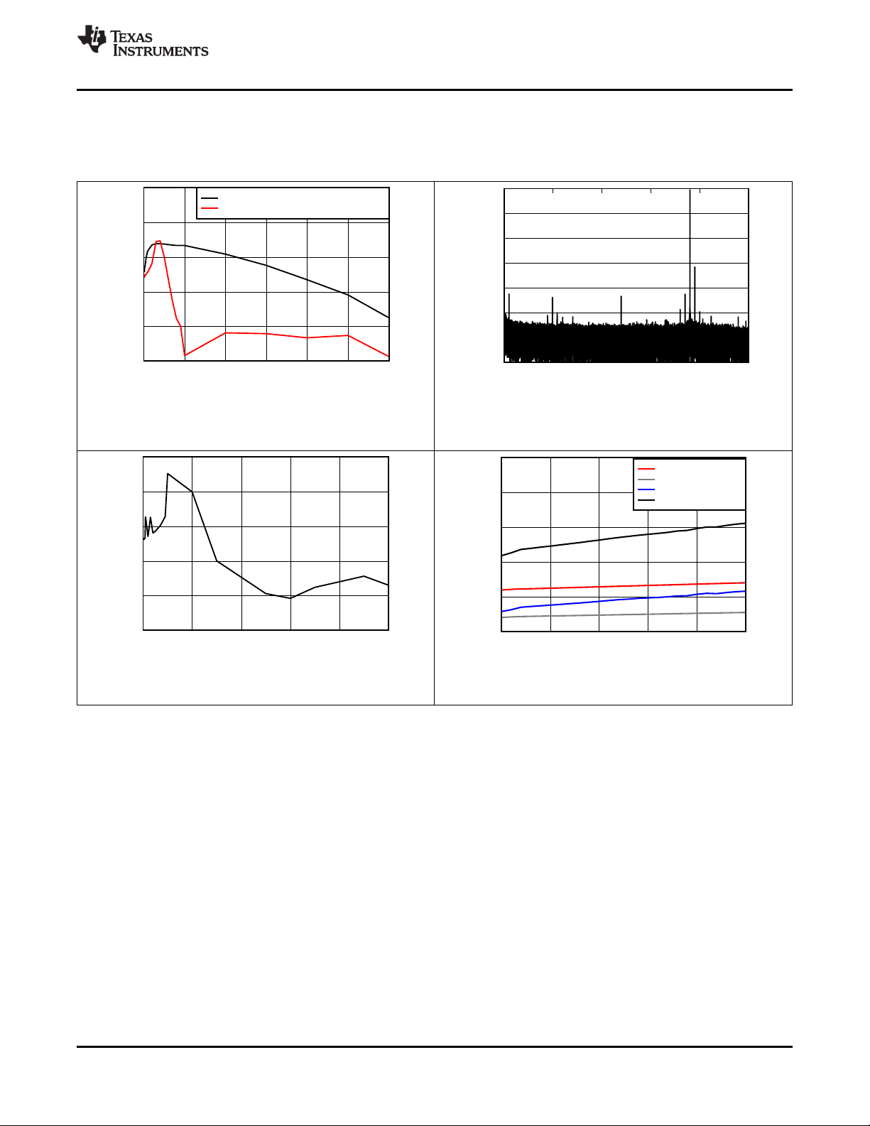
Figure 20. HD2 vs Input Frequency and Temperature Figure 21. SNR vs Input Frequency and AVDD19 Supply
Figure 22. HD3 vs Input Frequency and AVDD19 Supply Figure 23. SNR vs Input Frequency and AVDD Supply
Figure 24. HD3 vs Input Frequency and AVDD Supply Figure 25. SNR vs Input Frequency and DVDD Supply
Product Folder Links: ADS58J64
Submit Documentation FeedbackCopyright © 2017, Texas Instruments Incorporated
15
Input Frequency (MHz)
Amplitude (dBFS)
0 50 100 150 200 250
-140
-120
-100
-80
-60
-40
-20
0
D030
Intermodulation Distortion (dBFS)
Each Tone Amplitude (dBFS)
-35 -31 -27 -23 -19 -15 -11 -7
-120
-112
-104
-96
-88
-80
D029
Amplitude (dBFS)
Signal-to-Noise Ratio (dBFS)
Spurious-Free Dynamic Range (dBc, dBFS)
-70 -60 -50 -40 -30 -20 -10 0
67.5 0
68.5 30
69.5 60
70.5 90
71.5 120
72.5 150
D027
SNR (dBFS)
SFDR (dBc)
SFDR (dBFS)
Each Tone Amplitude (dBFS)
Intermodulation Distortion (dBFS)
-35 -31 -27 -23 -19 -15 -11 -7
-120
-112
-104
-96
-88
-80
D028
Input Frequency (MHz)
Third-Order Harmonic Distortion (dBc)
0 50 100 150 200 250 300 350 400 450 500
75
80
85
90
95
100
D025
DVDD = 1.1 V
DVDD = 1.15 V
DVDD = 1.2 V
Amplitude (dBFS)
Signal-to-Noise Ratio (dBFS)
Spurious-Free Dynamic Range (dBc, dBFS)
-70 -60 -50 -40 -30 -20 -10 0
69 0
69.5 30
70 60
70.5 90
71 120
71.5 150
D026
SNR (dBFS)
SFDR (dBc)
SFDR (dBFS)
ADS58J64
SBAS807A –JANUARY 2017–REVISED JANUARY 2017
Typical Characteristics: 14-Bit Burst Mode (continued)
www.ti.com
typical values are at TA= 25°C, full temperature range is from T
= –40°C to T
MIN
= +100°C, device sampling frequency =
MAX
1 GSPS, mode 8: 2x decimation with burst mode output, 50% clock duty cycle, AVDD19 = 1.9 V, AVDD = DVDD = 1.15 V,
–1-dBFS differential input, and fIN= 190 MHz (unless otherwise noted)
fIN= 190 MHz
Figure 26. HD3 vs Input Frequency and DVDD Supply
Figure 27. Performance vs Input Signal Amplitude
fIN= 370 MHz
Figure 28. Performance vs Input Signal Amplitude
f
= 340 MHz, f
IN1
16
Submit Documentation Feedback Copyright © 2017, Texas Instruments Incorporated
Figure 30. IMD vs Input Amplitude
IN2
= 350 MHz
fIN= 190 MHz, AIN= –1 dBFS, f
Product Folder Links: ADS58J64
f
= 160 MHz, f
IN1
= 170 MHz
IN2
Figure 29. IMD vs Input Amplitude
= 5 MHz,
A
= 50 mVPP, SFDR = 73.5 dBFS
Noise
Noise
Figure 31. Power-Supply Rejection Ratio FFT
for 50-mV Noise on AVDD Supply
Sampling Speed (MSPS)
Power Consumption (W)
250 300 350 400 450 500
0
0.8
1.6
2.4
3.2
4
D034
AVDD19_Power (W)
AVDD_Power (W)
DVDD_Power (W)
Total Power (W)
Frequency of Input Common-Mode Signal (MHz)
Common-Mode Rejection Ratio (dB)
0 20 40 60 80 100
-65
-55
-45
-35
-25
-15
D033
Input Frequency (MHz)
Amplitude (dBFS)
0 50 100 150 200 250
-140
-120
-100
-80
-60
-40
-20
0
D032
Frequency of Signal on Supply (MHz)
Power Supply Rejection Ratio (dB)
0 10 20 30 40 50 60
-60
-50
-40
-30
-20
-10
D031
PSRR with 50-mVPP Signal on AVDD
PSRR with 50-mVPP Signal on AVDD19
www.ti.com
Typical Characteristics: 14-Bit Burst Mode (continued)
ADS58J64
SBAS807A –JANUARY 2017–REVISED JANUARY 2017
typical values are at TA= 25°C, full temperature range is from T
= –40°C to T
MIN
= +100°C, device sampling frequency =
MAX
1 GSPS, mode 8: 2x decimation with burst mode output, 50% clock duty cycle, AVDD19 = 1.9 V, AVDD = DVDD = 1.15 V,
–1-dBFS differential input, and fIN= 190 MHz (unless otherwise noted)
fIN= 190 MHz, AIN= –1 dBFS, f
Figure 32. PSRR vs Power Supplies
Noise
= 5 MHz, A
Noise
= 50 mV
PP
fIN= 190 MHz, AIN= –1 dBFS, f
A
= 50 mVPP, SFDR = 63.12 dBFS
Noise
Noise
= 5 MHz,
Figure 33. Common-Mode Rejection Ratio FFT
fIN= 190 MHz, AIN= –1 dBFS, f
Figure 34. CMRR vs Noise Frequency
Noise
= 5 MHz, A
= 50 mV
Noise
PP
Product Folder Links: ADS58J64
Figure 35. Power Consumption vs Input Clock Rate
Submit Documentation FeedbackCopyright © 2017, Texas Instruments Incorporated
17
Input Frequency (MHz)
Amplitude (dBFS)
0 25 50 75 100 125
-140
-120
-100
-80
-60
-40
-20
0
D037
Input Frequency (MHz)
Amplitude (dBFS)
0 25 50 75 100 125
-140
-120
-100
-80
-60
-40
-20
0
D038
Input Frequency (MHz)
Amplitude (dBFS)
0 25 50 75 100 125
-140
-120
-100
-80
-60
-40
-20
0
D035
Input Frequency (MHz)
Amplitude (dBFS)
0 25 50 75 100 125
-140
-120
-100
-80
-60
-40
-20
0
D036
ADS58J64
SBAS807A –JANUARY 2017–REVISED JANUARY 2017
www.ti.com
6.10 Typical Characteristics: Mode 2
typical values are at TA= 25°C, full temperature range is from T
1 GSPS, mode 8: 2x decimation with burst mode output, 50% clock duty cycle, AVDD19 = 1.9 V, AVDD = DVDD = 1.15 V,
–1-dBFS differential input, and fIN= 190 MHz (unless otherwise noted)
= –40°C to T
MIN
= +100°C, device sampling frequency =
MAX
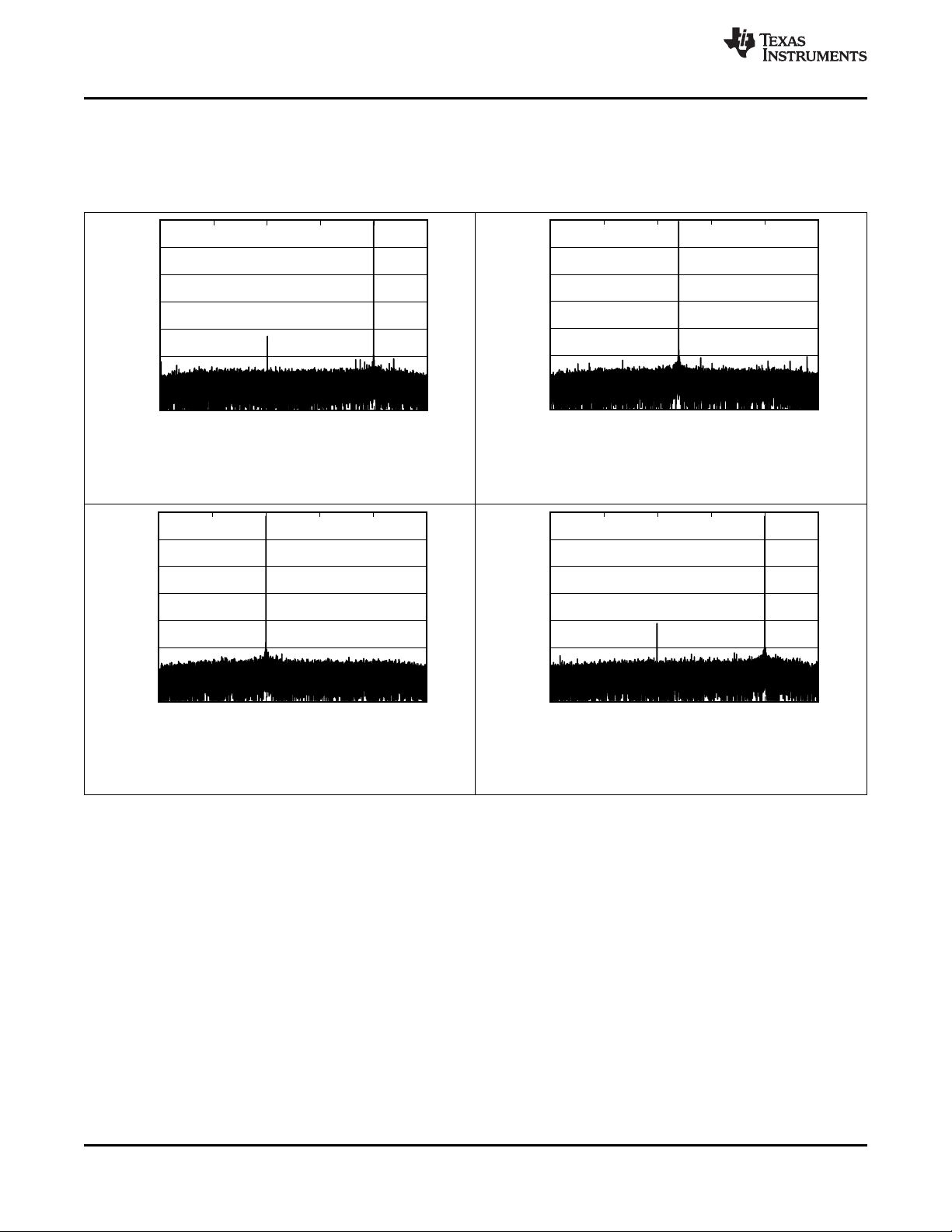
fIN= 150 MHz, AIN= –1 dBFS, SNR = 72.85 dBFS,
SFDR = 84.41 dBc, SFDR = 100.99 dBc (non 23)
Figure 36. FFT for 150-MHz Input Signal
fIN= 300 MHz, AIN= –3 dBFS, SNR = 72.3 dBFS,
SFDR = 100.31 dBc, SFDR = 100.75 dBc (non 23)
Figure 38. FFT for 300-MHz Input Signal
fIN= 190 MHz, AIN= –1 dBFS, SNR = 72.37 dBFS,
SFDR = 99.95 dBc, SFDR = 100.76 dBc (non 23)
Figure 37. FFT for 190-MHz Input Signal
fIN= 350 MHz, AIN= –3 dBFS, SNR = 72.02 dBFS,
SFDR = 79.23 dBc, SFDR = 96.42 dBc (non 23)
Figure 39. FFT for 350-MHz Input Signal
18
Submit Documentation Feedback Copyright © 2017, Texas Instruments Incorporated
Product Folder Links: ADS58J64
Input Frequency (MHz)
Amplitude (dBFS)
-125 -75 -25 25 75 125
-140
-120
-100
-80
-60
-40
-20
0
D041
Input Frequency (MHz)
Amplitude (dBFS)
-125 -75 -25 25 75 125
-140
-120
-100
-80
-60
-40
-20
0
D039
Input Frequency (MHz)
Amplitude (dBFS)
-125 -75 -25 25 75 125
-140
-120
-100
-80
-60
-40
-20
0
D040
ADS58J64
www.ti.com
SBAS807A –JANUARY 2017–REVISED JANUARY 2017
6.11 Typical Characteristics: Mode 0
typical values are at TA= 25°C, full temperature range is from T
1 GSPS, mode 8: 2x decimation with burst mode output, 50% clock duty cycle, AVDD19 = 1.9 V, AVDD = DVDD = 1.15 V,
–1-dBFS differential input, and fIN= 190 MHz (unless otherwise noted)
= –40°C to T
MIN
= +85°C, device sampling frequency =
MAX
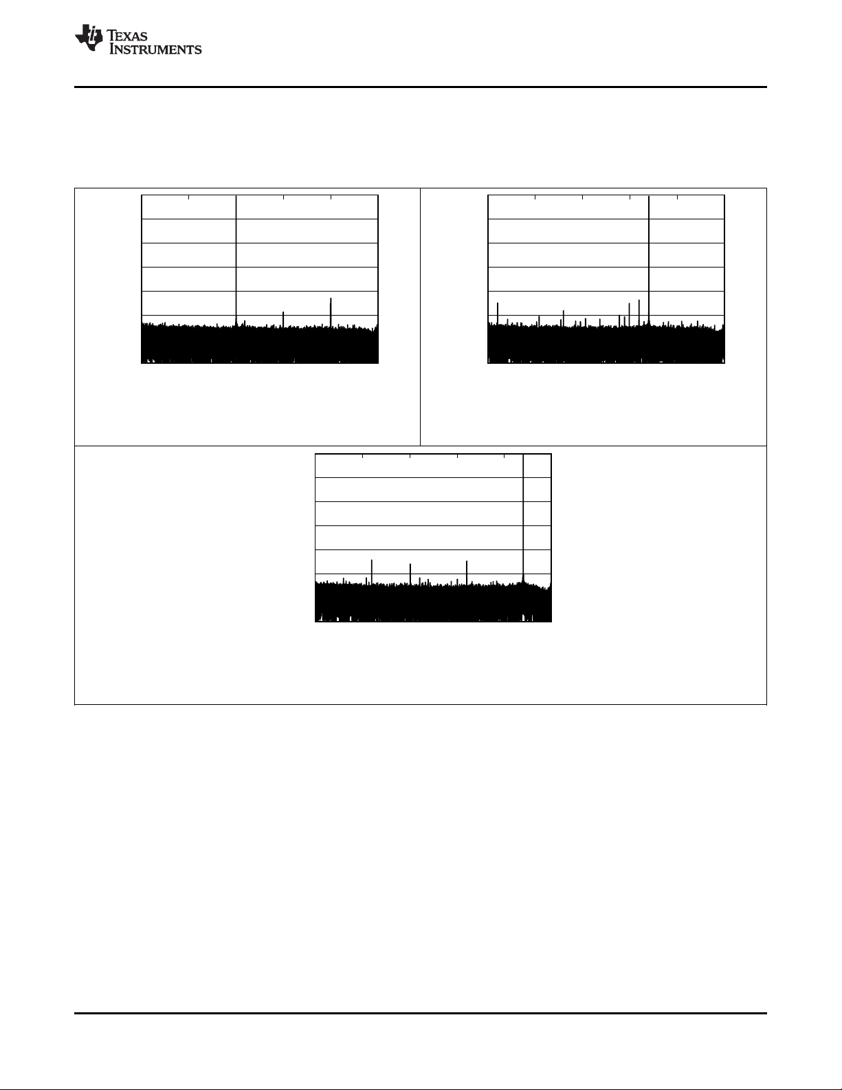
fIN= 100 MHz, AIN= –1 dBFS, SNR = 70.16 dBFS,
SFDR = 84.95 dBc, SFDR = 95.41 dBc (non 23)
Figure 40. FFT for 100-MHz Input Signal
fIN= 220 MHz, AIN= –1 dBFS, SNR = 69.27 dBFS,
SFDR = 87.66 dBc, SFDR = 91.04 dBc (non 23)
Figure 42. FFT for 220-MHz Input Signal
fIN= 170 MHz, AIN= –1 dBFS, SNR = 69.35 dBFS,
SFDR = 86.46 dBc, SFDR = 89.27 dBc (non 23)
Figure 41. FFT for 170-MHz Input Signal
Product Folder Links: ADS58J64
Submit Documentation FeedbackCopyright © 2017, Texas Instruments Incorporated
19
CLKINP, CLKINM
DAP, DAMINAP, INAM
PLL
x10/x20
DCP, DCM
DDP, DDM
INBP. INAM
INCP, INCM
INDP, INDM
DBP, DBM
JESD204B
SYNCbCD
SYSREFP, SYSREFM
RESET
SCAN_EN
SCLK
SEN
SDIN
SDOUT
Configuration
Registers
2x Decimation
High Pass/
Low Pass
2x Decimation
High Pass/
Low Pass
2x Decimation
High Pass/
Low Pass
2x Decimation
High Pass/
Low Pass
SYNCbAB
TRIGAB
TRIGCD
TRDYCD
JESD204B
TRDYAB
Burst Mode
Burst Mode
N
14bit
ADC
14-bit
ADC
14bit
ADC
14-bit
ADC
14bit
ADC
14bit
ADC
14-bit
ADC
14-bit
ADC
CLK
DIV
/2, /4
N
NCO
NCO
ADS58J64
SBAS807A –JANUARY 2017–REVISED JANUARY 2017
www.ti.com
7 Detailed Description
7.1 Overview
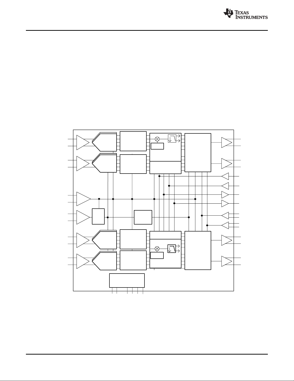
The ADS58J64 is a quad-channel device with a complex digital down-converter (DDC) and digital decimation to
allow flexible signal processing to suit different usage cases. Each channel is composed of two interleaved
analog-to-digital converters (ADCs) sampling at half the input clock rate. The 2x interleaved data are decimated
by 2 to provide a processing gain of 3 dB. The decimation filter can be configured as low pass (default) or high
pass. The half-rate (with regards to the input clock) data are available on the output, in burst mode (DDC mode =
8) as a stream of high (14-bit) and low (9-bit) resolution samples. Burst mode can be enabled by device
programming along with other options (such as the number of high- and low-resolution samples, and trigger
mode as either automatic or pin-controlled). In default mode, the device operates in DDC mode 0, where the
input is mixed with a constant frequency of –fS/ 4 and is given out as complex IQ. The different operational
modes modes of the ADS58J64 are listed in Table 1.
7.2 Functional Block Diagram
20
Submit Documentation Feedback Copyright © 2017, Texas Instruments Incorporated
Product Folder Links: ADS58J64
0.1 PF
0.1 PF
150 Ÿ
150 Ÿ
Z
0
Z
0
Typical LVPECL
Clock Input
CLKP
CLKM
Internal termination
of 100
ADS58J64
Copyright © 2017, Texas Instruments Incorporated
CLKP
CLKM
0.1 PF
0.1 PF
Z
0
Z
0
Typical LVDS
Clock Input
Internal termination
of 100
ADS58J64
Copyright © 2017, Texas Instruments Incorporated
INxP
INxM
1:1
0.1 PF
0.1 PF
1:1
25 :
0.1 PF
0.1 PF
TI Device
R
IN
C
IN
T2T1
25 :
10 :
10 :
Copyright © 2017, Texas Instruments Incorporated
ADS58J64
www.ti.com
SBAS807A –JANUARY 2017–REVISED JANUARY 2017
7.3 Feature Description
7.3.1 Analog Inputs
The ADS58J64 analog signal inputs are designed to be driven differentially. The analog input pins have internal
analog buffers that drive the sampling circuit. As a result of the analog buffer, the input pins present a highimpedance input across a very wide frequency range to the external driving source that enables great flexibility in
the external analog filter design as well as excellent 50-Ω matching for RF applications. The buffer also helps
isolate the external driving circuit from the internal switching currents of the sampling circuit, resulting in a more
constant SFDR performance across input frequencies. The common-mode voltage of the signal inputs is
internally biased to 1.3 V using 2-kΩ resistors to allow for ac-coupling of the input drive network. Each input pin
(INP, INM) must swing symmetrically between (VCM + 0.275 V) and (VCM – 0.275 V), resulting in a 1.1-V
(default) differential input swing. The input sampling circuit has a 3-dB bandwidth that extends up to 1000 MHz.
7.3.2 Recommended Input Circuit
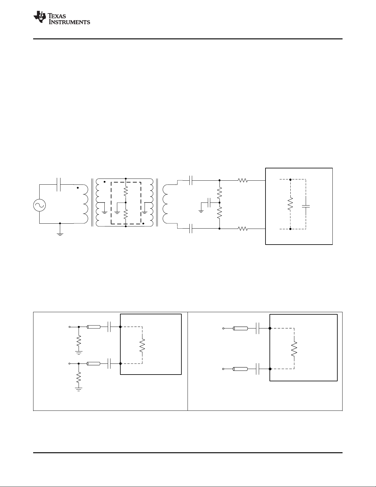
In order to achieve optimum ac performance, the following circuitry (shown in Figure 43) is recommended at the
analog inputs.
PP
Figure 43. Analog Input Driving Circuit
7.3.3 Clock Input
The clock inputs of the ADS58J64 supports LVDS and LVPECL standards. The CLKP, CLKM inputs have an
internal termination of 100 Ω. The clock inputs must be ac-coupled because the input pins are self-biased to a
common-mode voltage of 0.7 V, as shown in Figure 44 and Figure 45.
Figure 45. LVDS Clock Driving Circuit
Figure 44. LVPECL Clock Driving Circuit
Product Folder Links: ADS58J64
Submit Documentation FeedbackCopyright © 2017, Texas Instruments Incorporated
21
2
ADC
fS = 1 GSPS
Real or IQ Output
IQ Output
Real Output
JESD204B
Block
f
OUT
/ 4
2
500 MSPS
Filter
IQ 500 MSPS
Filter
2
Filter
IQ 250 MSPS
IQ 125 MSPS
16-Bit
NCO
ADS58J64
SBAS807A –JANUARY 2017–REVISED JANUARY 2017
www.ti.com
7.4 Device Functional Modes
7.4.1 Digital Features
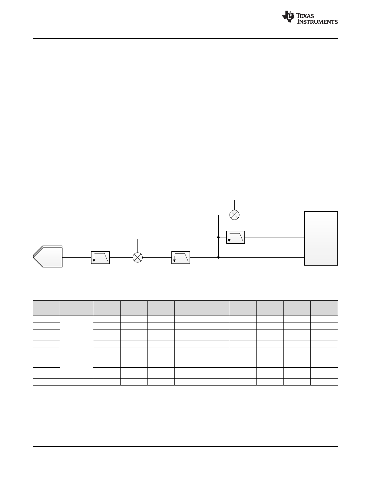
The ADS58J64 has two stages of digital decimation filters, as shown in Figure 46. The first stage is mandatory
and decimates by 2, and can be configured as either a low-pass or high-pass filter. The second stage decimation
supports real to complex quadrature demodulation and decimation by 2 or 4. After decimation, the complex
signal can be converter back to a real signal through digital quadrate modulation at a frequency of f
f
is the sample frequency after decimation.
OUT
Optionally, a burst mode output can be used to output the decimate-by-2 data directly.
The four channels can be configured as pairs (A, B and C, D) to either burst or decimation mode. If all four
channels are in decimation mode, then the decimation setting must be the same decimation for all four channels.
All modes of operation and the maximum bandwidth provided at a sample rate of 491.52 MSPS and
368.64 MSPS are listed in Table 1. The first stage decimation filter prior to the 16-bit numerically controlled
oscillator (NCO) is a noise suppression filter with 45% pass-band bandwidth relative to the input sample rate,
less than 0.2-dB ripple, and approximately 40-dB stop-band attenuation. This filter is only used to reduce the
ADC output rate from 1 GSPS to 500 MSPS prior to the second stage decimation filter or burst mode. Some
analog filtering of other Nyquist zones after the first stage decimation filter is expected to be required.
The second stage filter has a pass-band bandwidth of 81.4% relative to the output sample rate, supporting a
200-MHz bandwidth with a 245.76-MSPS complex output rate.
/ 4, where
OUT
Figure 46. ADS58J64 Channel (1 of 4) Block Diagram
Table 1. ADS58J64 Operating Modes
OPERATING
MODE
0
1 2 16-bit NCO 2 200 MHz 150 MHz — Complex 250 MSPS
2 2 — 2
3 2 16-bit NCO Bypass 200 MHz 150 MHz f
4 2 16-bit NCO 2 100 MHz 75 MHz f
5 Reserved Reserved Reserved Reserved Reserved Reserved Reserved Reserved
6 2 16-bit NCO 4 100 MHz 75 MHz — Complex 125 MSPS
7 2 16-bit NCO 2 100 MHz 75 MHz f
8 Burst mode — — — 223 MHz 167 MHz — Real 500 MSPS
22
DESCRIPTION
Decimation
Submit Documentation Feedback Copyright © 2017, Texas Instruments Incorporated
1ST STAGE
DECIMATION
2 ±fS/ 4 2 200 MHz 150 MHz — Complex 250 MSPS
DIGITAL
MIXER
2ND STAGE
DECIMATION
Product Folder Links: ADS58J64
BANDWIDTH AT
491.52 MSPS
100 MHz (LP, LP or HP, HP),
75 MHz (HP, LP or LP, HP)
BANDWIDTH
AT 368.64
56.25 MHz
MSPS
75 MHz,
OUTPUT
MIXER
— Real 250 MSPS
OUT
OUT
OUT
OUTPUT
FORMAT
/ 4 Real 500 MSPS
/ 4 Real 250 MSPS
Real with zero
/ 4
insertion
MAX
OUTPUT
RATE
500 MSPS
Frequency (MHz)
Gain (dB)
0 50 100 150 200 250 300 350 400 450 500 550
-45
-40
-35
-30
-25
-20
-15
-10
-5
0
D042
Frequency (MHz)
Gain (dB)
0 50 100 150 200 250 300 350 400 450 500 550
-1
-0.9
-0.8
-0.7
-0.6
-0.5
-0.4
-0.3
-0.2
-0.1
0
D043
u
S
NCO
16
NCO Frequency [n] f
f
2
ADS58J64
www.ti.com
SBAS807A –JANUARY 2017–REVISED JANUARY 2017
7.4.1.1 Numerically Controlled Oscillators (NCOs) and Mixers
The ADS58J64 is equipped with a complex numerically-controlled oscillator. The oscillator generates a complex
exponential sequence: x[n] = e
jωn
. The frequency (ω) is specified by the 16-bit register setting. The complex
exponential sequence is multiplied by the real input from the ADC to mix the desired carrier down to 0 Hz.
The NCO frequency setting is set by the 16-bit register value, NCO_FREQ[n]:
(1)
7.4.1.2 Decimation Filter
The ADS58J64 has two decimation filters (decimate-by-2) in the data path. The first stage of the decimation filter
is non-programmable and is used in all functional modes. The second stage of decimation, available in DDC
mode 2 and 6, can be used to obtain noise and linearity improvement for low bandwidth applications.
7.4.1.2.1 Stage-1 Filter
The first stage filter is used for decimation of the 2x interleaved data from f
CLK
to f
/ 2. The frequency
CLK
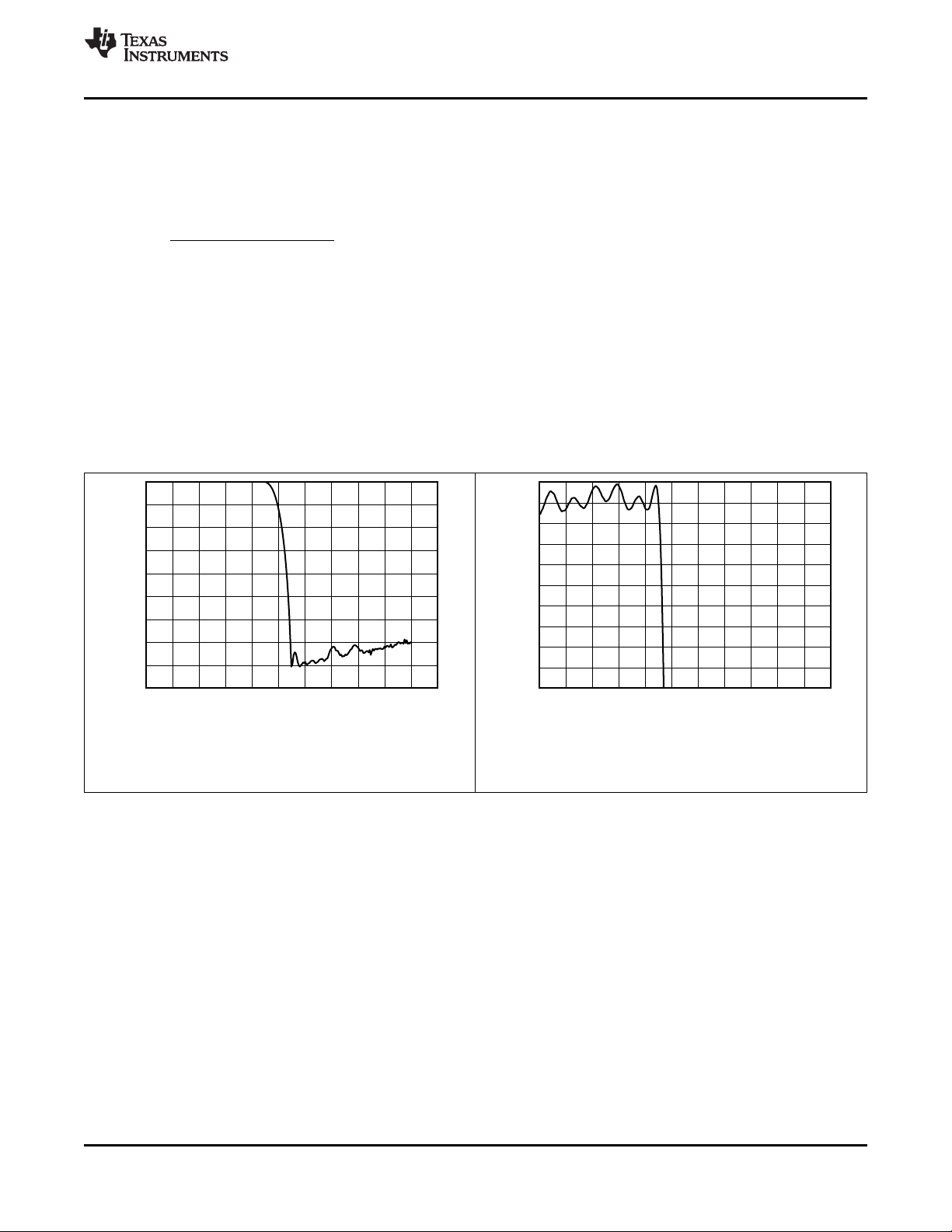
response and pass-band ripple of the first stage decimation filter are shown in Figure 47 and Figure 48,
respectively.
Input clock rate = 1 GHz
Figure 47. Decimation Filter Response vs Frequency
Figure 48. Decimation Filter Pass-Band Ripple vs
Product Folder Links: ADS58J64
Input clock rate = 1 GHz
Frequency
Submit Documentation FeedbackCopyright © 2017, Texas Instruments Incorporated
23

2
ADC
fS = 1 GSPS
JESD204B
Block
500 MSPS
Filter
IQ 500 MSPS
Filter
IQ 250 MSPS
± fS / 4
2
-fS / 8
fS / 8
-fS / 4 -fS / 8
fS / 8 fS / 4
-fS / 2 -fS / 4
fS / 4 fS / 2
fS / 2
500 MHz
fS / 4
40 dBc
0
40 dBc 90 dBc
Frequency (MHz)
Gain (dB)
0 25 50 75 100 125 150 175 200 225 250 275
-110
-100
-90
-80
-70
-60
-50
-40
-30
-20
-10
0
D044
Frequency (MHz)
Gain (dB)
0 25 50 75 100 125 150 175 200 225 250 275
-1
-0.9
-0.8
-0.7
-0.6
-0.5
-0.4
-0.3
-0.2
-0.1
0
D045
ADS58J64
SBAS807A –JANUARY 2017–REVISED JANUARY 2017
7.4.1.2.2 Stage-2 Filter
The second stage filter is used for decimating the data from a sample rate of f
CLK
/ 2 to f
/ 4. The frequency
CLK
www.ti.com
response and pass-band ripple of the second stage filter are shown in Figure 49 and Figure 50, respectively.
Input clock rate (f
Figure 49. Decimation Filter Response vs Frequency
) = 1 GHz
CLK
Input clock rate (f
) = 1 GHz
CLK
Figure 50. Decimation Filter Pass-Band Ripple vs
Frequency
7.4.1.3 Mode 0: Decimate-by-4 With IQ Outputs and fS/ 4 Mixer
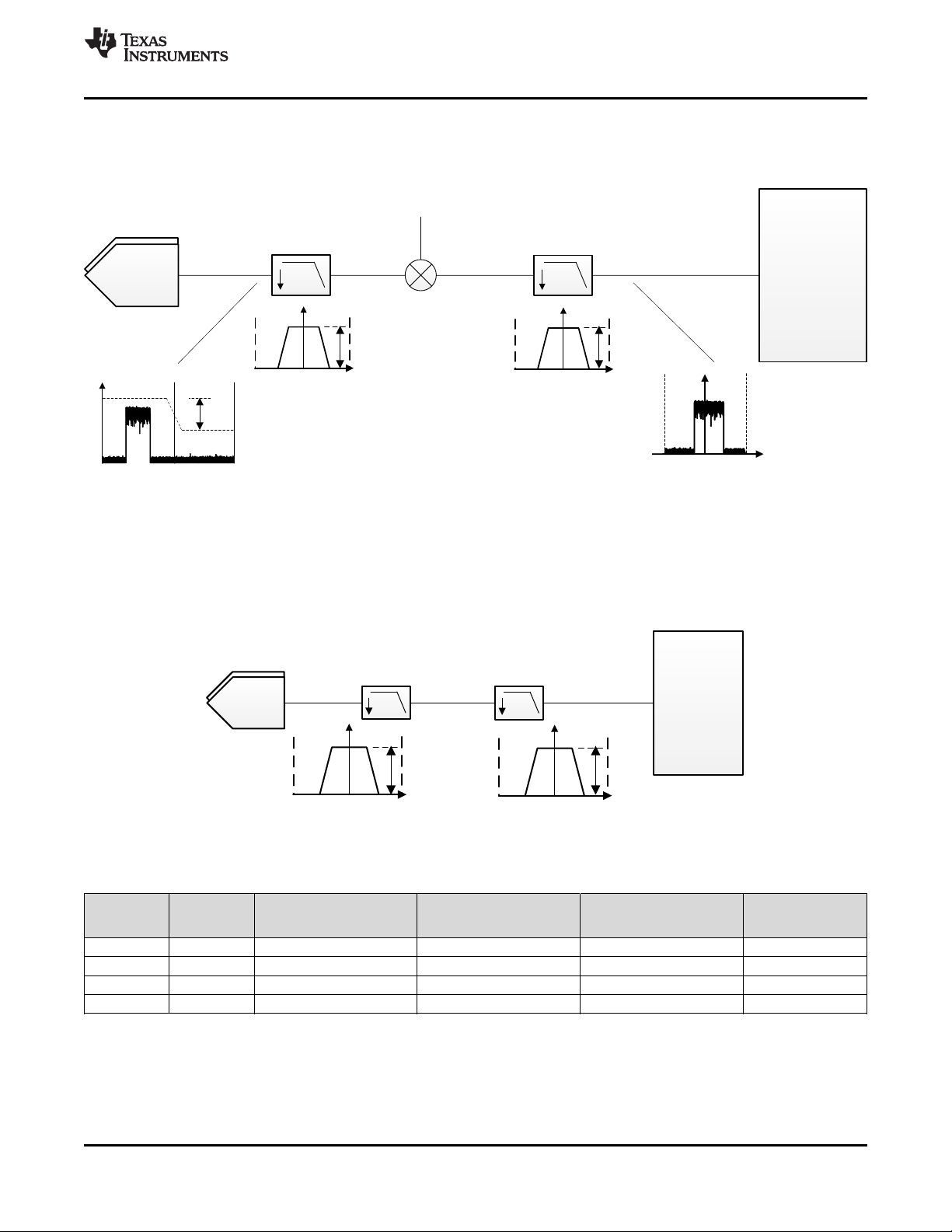
In mode 0, the DDC block includes a fixed frequency ±fS/ 4 complex digital mixer preceding the second stage
decimation filters. The IQ passband is approximately ±100 MHz centered at fS/ 8 or 3fS/ 8, as shown in
Figure 51.
24
Submit Documentation Feedback Copyright © 2017, Texas Instruments Incorporated
Figure 51. Operating Mode 0
Product Folder Links: ADS58J64
2
ADC
fS = 1 GSPS
JESD204B
Block
500 MSPS
Filter
Filter
Real 250 MSPS
2
-fS / 4 -fS / 8
fS / 8 fS / 4
90 dBc
-fS / 2 -fS / 4
fS / 4 fS / 2
40 dBc
2
ADC
fS = 1 GSPS
JESD204B
Block
500 MSPS
Filter
IQ 500 MSPS
Filter
IQ 250 MSPS
16-Bit
NCO
2
-fS / 8
fS / 8
fS / 2
500 MHz
fS / 4
40 dBc
0
-fS / 4 -fS / 8
fS / 8 fS / 4
-fS / 2 -fS / 4
fS / 4 fS / 2
40 dBc 90 dBc
ADS58J64
www.ti.com
SBAS807A –JANUARY 2017–REVISED JANUARY 2017
7.4.1.4 Mode 1: Decimate-by-4 With IQ Outputs and 16-Bit NCO
In mode 1, the DDC block includes a 16-bit frequency resolution complex digital mixer preceding the second
stage decimation filters, as shown in Figure 52.
Figure 52. Operating Mode 1
7.4.1.5 Mode 2: Decimate-by-4 With Real Output
In mode 2, the DDC block cascades two decimate-by-2 filters. Each filter can be configured as low pass (LP) or
high pass (HP) to allow down conversion of different frequency ranges, as shown in Table 2. The LP, HP and
HP, LP output spectra are inverted as shown in Figure 53.
Figure 53. Operating in Mode 2
Table 2. ADS58J64 Operating Mode 2 Down-Converted Frequency Ranges
1ST STAGE
FILTER
LP LP 0 MHz–100 MHz 100 MHz 0MHz–75 MHz 75 MHz
LP HP 150 MHz–223 MHz 73 MHz 112.5 MHz–167.25 MHz 54.75 MHz
HP LP 268.52 MHz–341.52 MHz 73 MHz 201.39 MHz–256.14 MHz 54.75 MHz
HP HP 391.52 MHz–491.52 MHz 100 MHz 293.64 MHz–368.64 MHz 75 MHz
2ND STAGE
FILTER
FREQUENCY RANGE WITH
CLOCK RATE OF 983.04 MHz
BANDWIDTH WITH CLOCK
RATE OF 983.04 MHz
FREQUENCY RANGE WITH
CLOCK RATE OF 737.28 MHz
BANDWIDTH WITH
CLOCK RATE OF
737.28 MHz
Product Folder Links: ADS58J64
Submit Documentation FeedbackCopyright © 2017, Texas Instruments Incorporated
25
2
ADC
fS = 1 GSPS
JESD204B
Block
500 MSPS
Filter
IQ 500 MSPS
16-Bit
NCO
f
OUT
/ 4
Real Output
2
Filter
IQ 250 MSPS
-fS / 4 -fS / 8
fS / 8 fS / 4
90 dBc
-fS / 2 -fS / 4
fS / 4 fS / 2
40 dBc
2
ADC
fS = 1 GSPS
JESD204B
Block
500 MSPS
Filter
IQ 500 MSPS
16-Bit
NCO
f
OUT
/ 4
Real Output
Filter
-fS / 2 -fS / 4
fS / 4 fS / 2
40 dBc
ADS58J64
SBAS807A –JANUARY 2017–REVISED JANUARY 2017
www.ti.com
7.4.1.6 Mode 3: Decimate-by-2 Real Output With Frequency Shift
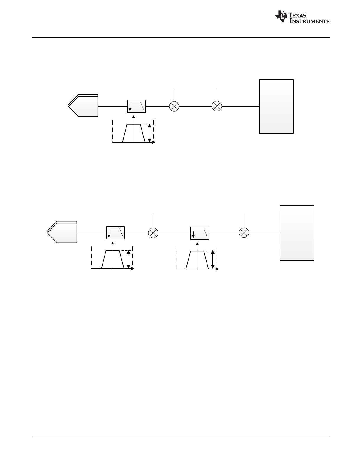
In mode 3, the DDC block includes a 16-bit complex NCO digital mixer followed by a fS/ 4 mixer with a real
output to center the band at fS/ 4. The NCO must be set to a value different from ±fS/ 4, or else the samples are
zeroed as shown in Figure 54.
Figure 54. Operating Mode 3
7.4.1.7 Mode 4: Decimate-by-4 With Real Output
In mode 4, the DDC block includes a 16-bit complex NCO digital mixer preceding the second stage decimation
filter. The signal is then mixed with f
/ 4 to generate a real output, as shown in Figure 55. The bandwidth
OUT
available in this mode is 100 MHz.
26
Figure 55. Operating Mode 4
Submit Documentation Feedback Copyright © 2017, Texas Instruments Incorporated
Product Folder Links: ADS58J64
 Loading...