

Page 1
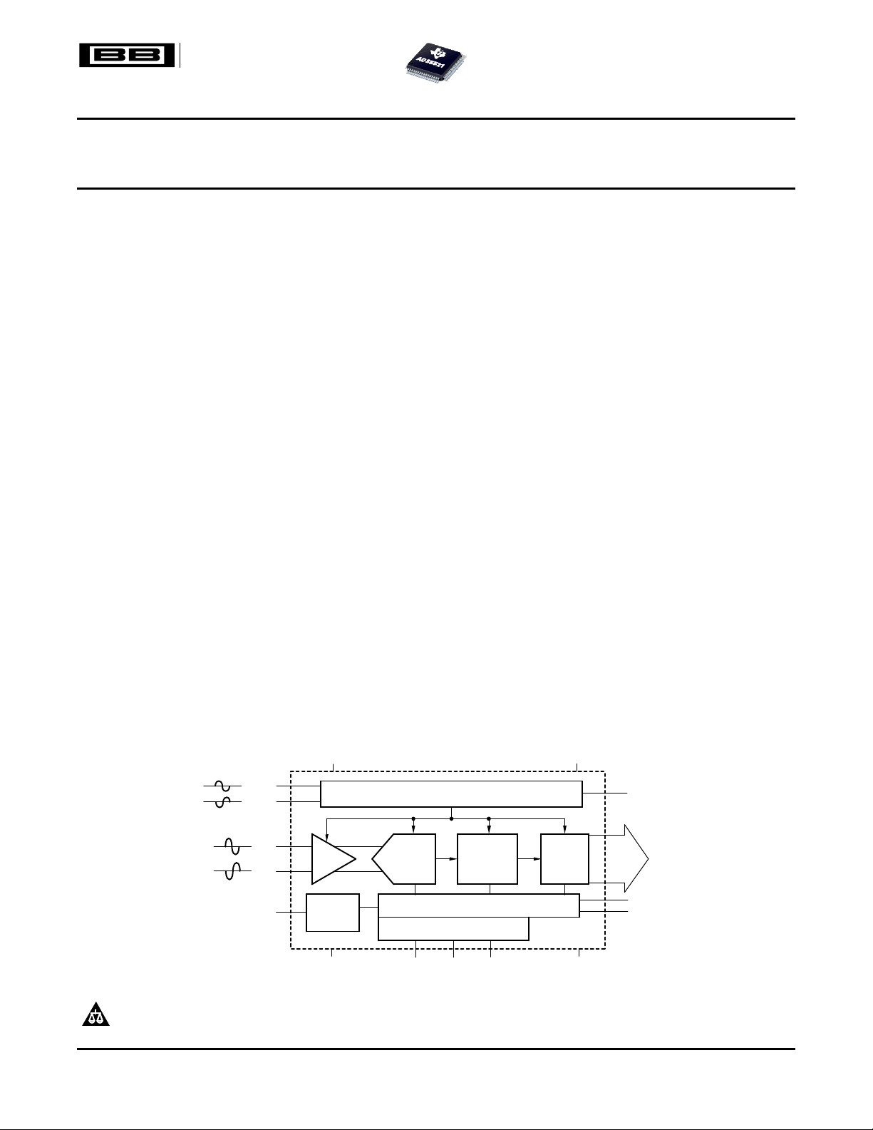
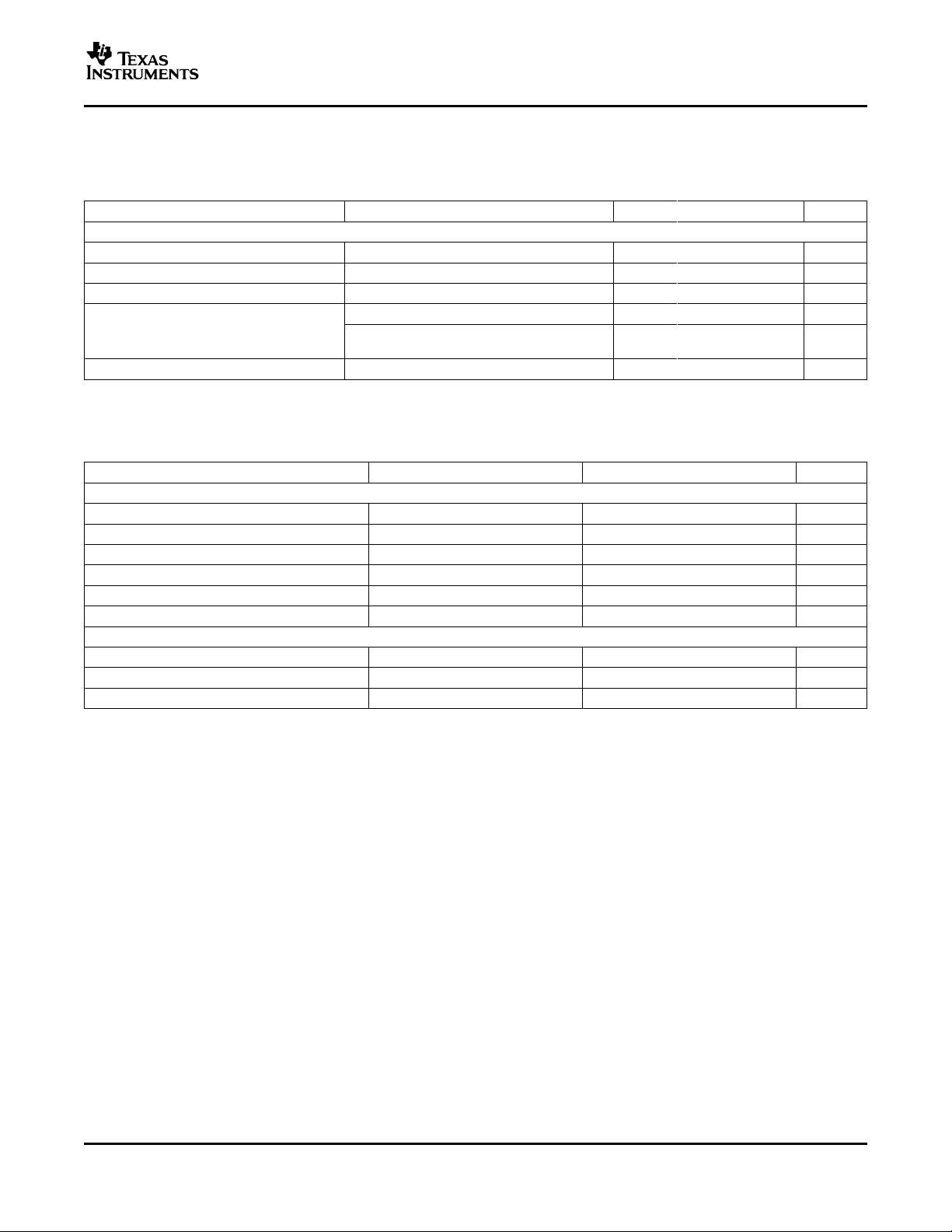
12−Bit
Pipeline
ADC Core
S&H
CLK+
CLK
−
CLKOUT
VIN+
V
IN
−
Digital
Error
Correction
Timing Circuitry
Internal
Reference
Control Logic
Serial Programming Register
Output
Control
AV
DD
D0
.
.
.
D11
CM
OVR
DFS
ADS5521
A
GND
DR
GND
SEN SDATA
SCLK
DRV
DD
Analog-To-Digital Converter
ADS5521
SBAS309A – MAY 2004 – REVISED APRIL 2005
12-Bit, 105MSPS
FEATURES
• 12-Bit Resolution
• 105MSPS Sample Rate
• High SNR: 70dBFS at 100MHz f
• High SFDR: 86dBc at 100MHz f
• 2.3V
• Internal Voltage Reference
• 3.3V Single-Supply Voltage
• Analog Power Dissipation: 571mW
– Output Buffer Power: 165mW
• Pin-Compatible with:
ADS5500 (14-Bit, 125MSPS)
ADS5541 (14-Bit, 105MSPS)
ADS5542 (14-Bit, 80MSPS)
ADS5520 (12-Bit, 125MSPS)
ADS5522 (12-Bit, 80MSPS)
Differential Input Voltage
PP
IN
IN
• TQFP-64 PowerPAD™ Package
• Recommended Op Amps:
THS3201, THS3202, THS4503, THS4509,
THS9001, OPA695, OPA847
APPLICATIONS
• Wireless Communication
– Communication Receivers
– Base Station Infrastructure
• Test and Measurement Instrumentation
• Single and Multichannel Digital Receivers
• Communication Instrumentation
– Radar
– Infrared
• Video and Imaging
• Medical Equipment
• Military Equipment
DESCRIPTION
The ADS5521 is a high-performance, 12-bit, 105MSPS analog-to-digital converter (ADC). To provide a complete
converter solution, it includes a high-bandwidth linear sample-and-hold stage (S&H) and internal reference.
Designed for applications demanding the highest speed and highest dynamic performance in very little space,
the ADS5521 has excellent analog power dissipation of 571mW and output buffer power dissipation of 165mW
from a 3.3V single-supply voltage. This allows an even higher system integration density. The provided internal
reference simplifies system design requirements. Parallel CMOS-compatible output ensures seamless interfacing
with common logic.
The ADS5521 is available in a 64-pin TQFP PowerPAD package and is pin-compatible with the ADS5500,
ADS5541, ADS5542, ADS5520, and ADS5522. This device is specified over the full temperature range of –40°C
to +85°C.
PowerPAD is a trademark of Texas Instruments.
PRODUCTION DATA information is current as of publication date.
Products conform to specifications per the terms of the Texas
Instruments standard warranty. Production processing does not
necessarily include testing of all parameters.
Please be aware that an important notice concerning availability, standard warranty, and use in critical applications of Texas
Instruments semiconductor products and disclaimers thereto appears at the end of this data sheet.
Copyright © 2004–2005, Texas Instruments Incorporated
Page 2
www.ti.com
ADS5521
SBAS309A – MAY 2004 – REVISED APRIL 2005
This integrated circuit can be damaged by ESD. Texas Instruments recommends that all integrated
circuits be handled with appropriate precautions. Failure to observe proper handling and installation
procedures can cause damage.
ESD damage can range from subtle performance degradation to complete device failure. Precision
integrated circuits may be more susceptible to damage because very small parametric changes could
cause the device not to meet its published specifications.
ORDERING INFORMATION
(1)
SPECIFIED
PACKAGE TEMPERATURE PACKAGE ORDERING TRANSPORT
PRODUCT PACKAGE-LEAD DESIGNATOR RANGE MARKING NUMBER MEDIA, QUANTITY
ADS5521 PAP –40C to +85C ADS5521I
HTQFP-64
PowerPAD
(2)
ADS5521IPAP Tray, 160
ADS5521IPAPR Tape and Reel, 1000
(1) For the most current package and ordering information, see the Package Option Addendum, or see the TI web site at www.ti.com .
(2) Thermal pad size: 3.5mm x 3.5mm (min), 4mm x 4mm (max). θJA= 21.47 ° C/W and θJC= 2.99 ° C/W, when used with 2 oz. copper trace
and pad soldered directly to a JEDEC standard, four-layer, 3 in x 3 in PCB.
ABSOLUTE MAXIMUM RATINGS
over operating free-air temperature range (unless otherwise noted)
AV
to A
Supply Voltage
Analog input to A
Logic input to DR
Digital data output to DR
DD
A
GND
GND
GND
GND
, DRV
GND
to DR
GND
Operating temperature range –40 to +85 °C
Junction temperature +105 °C
Storage temperature range –65 to +150 °C
(1) Stresses above these ratings may cause permanent damage. Exposure to absolute maximum conditions for extended periods may
degrade device reliability. These are stress ratings only, and functional operation of the device at these or any other conditions beyond
those specified is not implied.
to DR
DD
(1)
ADS5521 UNIT
GND
–0.3 to +3.7 V
±0.1 V
–0.3 to minimum (AVDD + 0.3, 3.6) V
–0.3 to DRV
–0.3 to DRV
DD
DD
V
V
RECOMMENDED OPERATING CONDITIONS
PARAMETER MIN TYP MAX UNIT
Supplies
Analog supply voltage, AV
Output driver supply voltage, DRV
Analog input
Differential input range 2.3 V
Input common-mode voltage, V
Digital Output
Maximum output load 10 pF
Clock Input
ADCLK input sample rate (sine wave) 1/t
Clock amplitude, sine wave, differential
Clock duty cycle
Open free-air temperature range –40 +85 °C
(3)
DD
DD
(1)
CM
C
(2)
DLL ON 60 105 MSPS
DLL OFF 2 80 MSPS
(1) Input common-mode should be connected to CM.
(2) See Figure 48 for more information.
(3) See Figure 47 for more information.
2
3.0 3.3 3.6 V
3.0 3.3 3.6 V
1.45 1.55 1.65 V
1 3 V
50 %
PP
PP
Page 3
www.ti.com
ADS5521
SBAS309A – MAY 2004 – REVISED APRIL 2005
ELECTRICAL CHARACTERISTICS
Typical values given at TA= +25 ° C, min and max specified over the full temperature range of –40 ° C to +85 ° C, AV
DRV
= 3.3V, sampling rate = 105MSPS, 50% clock duty cycle, DLL On, 3V
DD
differential clock, and –1dBFS differential
PP
input, unless otherwise noted.
PARAMETER CONDITIONS MIN TYP MAX UNIT
Resolution 12 Bits
Analog Inputs
Differential input range 2.3 V
Differential input capacitance See Figure 39 4 pF
Analog input common-mode current
(per input)
Analog input bandwidth Source impedance = 50 Ω 750 MHz
Voltage overload recovery time 4
Internal Reference Voltages
Reference bottom voltage, V
Reference top voltage, V
REFM
REFP
Reference error –4 ±0.9 +4 %
Common-mode voltage output, V
CM
1.50 1.55 1.60 V
Dynamic DC Characteristics and Accuracy
No missing codes Tested
Differential nonlinearity error, DNL fIN= 55MHz –0.5 ±0.25 +0.5 LSB
Integral nonlinearity error, INL fIN= 55MHz –1.5 ±0.55 +1.5 LSB
Offset error ±1.5 mV
Offset temperature coefficient 0.02 %/°C
DC power-supply rejection ratio, DC PSRR 0.25 mV/V
∆ offset error/ ∆ AV
AV
= 3.6V
DD
from AV
DD
DD
= 3.0V to
Gain error ±0.3 %FS
Gain temperature coefficient –0.02 ∆ %/°C
Dynamic AC Characteristics
fIN= 10MHz 71 dBFS
fIN= 55MHz
+25°C to +85°C 68.0 70.5 dBFS
Full temp range 66.8 69.0 dBFS
Signal-to-noise ratio. SNR fIN= 70MHz 70.3 dBFS
fIN= 100MHz 70.0 dBFS
fIN= 150MHz 69.3 dBFS
fIN= 220MHz 67.8 dBFS
RMS idle channel noise Input tied to common-mode 0.32 LSB
fIN= 10MHz 83.0 dBc
fIN= 55MHz
Room temp 78.0 86.0 dBc
Full temp range 76.0 85.0 dBc
Spurious-free dynamic range, SFDR fIN= 70MHz 81.0 dBc
fIN= 100MHz 86.0 dBc
fIN= 150MHz 75.0 dBc
fIN= 220MHz 72.0 dBc
250 µA
1.0 V
2.15 V
=
DD
PP
Clock
cycles
3
Page 4
www.ti.com
ADS5521
SBAS309A – MAY 2004 – REVISED APRIL 2005
ELECTRICAL CHARACTERISTICS (continued)
Typical values given at TA= +25 ° C, min and max specified over the full temperature range of –40 ° C to +85 ° C, AV
DRV
input, unless otherwise noted.
= 3.3V, sampling rate = 105MSPS, 50% clock duty cycle, DLL On, 3V
DD
PARAMETER CONDITIONS MIN TYP MAX UNIT
fIN= 10MHz 90.0 dBc
fIN= 55MHz
Second-harmonic, HD2 fIN= 70MHz 81.0 dBc
fIN= 100MHz 88.0 dBc
fIN= 150MHz 75.0 dBc
fIN= 220MHz 72.0 dBc
fIN= 10MHz 83.0 dBc
fIN= 55MHz
Third-harmonic, HD3 fIN= 70MHz 87.0 dBc
fIN= 100MHz 86.0 dBc
fIN= 150MHz 80.0 dBc
fIN= 220MHz 78.0 dBc
Worst-harmonic/spur (other than HD2 and
HD3)
Signal-to-noise + distortion, SINAD fIN= 70MHz 69.6 dBFS
Total harmonic distortion, THD fIN= 70MHz 78.0 dBc
Effective number of bits, ENOB fIN= 55MHz 11.3 Bits
Two-tone intermodulation distortion, IMD f = 50.1MHz, 55.1MHz (-7dBFS each tone) 96.6 dBFS
fIN= 55MHz 87.0 dBc
fIN= 10MHz 70.7 dBFS
fIN= 55MHz
fIN= 100MHz 69.3 dBFS
fIN= 150MHz 68.2 dBFS
fIN= 220MHz 65.8 dBFS
fIN= 10MHz 79.0 dBc
fIN= 55MHz
fIN= 100MHz 84.0 dBc
fIN= 150MHz 74.0 dBc
fIN= 220MHz 70.3 dBc
f = 10.1MHz, 15.1MHz (-7dBFS each tone) 94.6 dBFS
f = 150.1MHz, 155.1MHz (-7dBFS each tone) 84.7 dBFS
Room temp 78.0 86.0 dBc
Full temp range 76.0 85.0 dBc
Room temp 78.0 88.0 dBc
Full temp range 76.0 87.0 dBc
Room temp 67.0 70.0 dBFS
Full temp range 65.8 68.5 dBFS
Room temp 76.0 83.0 dBc
Full temp range 74.0 82.0 dBc
differential clock, and –1dBFS differential
PP
=
DD
4
Page 5
www.ti.com
ADS5521
SBAS309A – MAY 2004 – REVISED APRIL 2005
ELECTRICAL CHARACTERISTICS (continued)
Typical values given at TA= +25 ° C, min and max specified over the full temperature range of –40 ° C to +85 ° C, AV
DRV
= 3.3V, sampling rate = 105MSPS, 50% clock duty cycle, DLL On, 3V
DD
differential clock, and –1dBFS differential
PP
input, unless otherwise noted.
PARAMETER CONDITIONS MIN TYP MAX UNIT
Power Supply
Total supply current, ICC fIN= 55MHz 223 250 mA
Analog supply current, IAVDD fIN= 55MHz 173 185 mA
Output buffer supply current, IDRVDD fIN= 55MHz 50 65 mA
Analog only 571 611 mW
Power dissipation
Output buffer power with 10pF load on digital
output to ground
165 215 mW
Standby power With Clocks running 180 250 mW
DIGITAL CHARACTERISTICS
Valid over full temperature range of T
otherwise noted.
PARAMETER CONDITIONS MIN TYP MAX UNIT
Digital Inputs
High-level input voltage, V
Low-level input voltage, V
High-level input current, I
Low-level input current, I
Input current for RESET –20 µA
Input capacitance 4 pF
Digital Outputs
Low-level output voltage, V
High-level output voltage, V
Output capacitance 3 pF
IH
IL
IH
IL
OL
OH
= –40°C to T
MIN
MAX
= +85°C, AV
= DRV
DD
= 3.3V, and 3V
DD
differential clock, unless
PP
2.4 V
C
= 10pF 0.3 0.4 V
LOAD
C
= 10pF 2.4 3.0 V
LOAD
DD
0.8 V
10 µA
10 µA
=
5
Page 6
www.ti.com
NOTE: It isrecommended thattheloading at CLKOUTand all data lines areaccurately matched to ensure thattheabove timing
matchescloselywith the specifiedvalues.
N
Sample
Analog
Input
Signal
Input Clock
Data Invalid
Output Clock
Data Out
(D0 to D11)
N−17 N−16 N−15 N−14 N−13 N−3 N−2 N−1 N
16.5 Clock Cycles
N + 2
N + 3
N + 4
N + 14
t
HOLD
t
A
t
START
t
END
t
SETUP
t
PDI
= t
START
+ t
SETUP
N + 15
N + 16
N + 17
ADS5521
SBAS309A – MAY 2004 – REVISED APRIL 2005
TIMING CHARACTERISTICS
Typical values given at TA= +25 ° C, min and max specified over the full temperature range of –40 ° C to +85 ° C, AV
DRV
otherwise noted.
(1) Timing parameters are ensured by design and characterization, and not tested in production.
(2) See Table 5 through Table 8 in the Application Information section for timing information at additional sampling frequencies.
(3) Data valid refers to 2.0V for LOGIC HIGH and 0.8V for LOGIC LOW.
(4) Refer to the Output Information section for details on using the input clock for data capture.
(5) Data outputs are available within a clock from assertion of OE; however, it takes 1000 clock cycles to ensure stable timing with respect
= 3.3V, sampling rate = 105MSPS, 50% clock duty cycle, 3V
DD
PARAMETER DESCRIPTION MIN TYP MAX UNIT
Switching Specification
Aperture delay, t
A
Aperture jitter (uncertainty) Uncertainty in sampling instant 300 fs
Data setup time, t
Data hold time, t
Input clock to output data valid start, Input clock rising edge to data valid start delay 1.9 2.8 ns
(4)
t
START
Input clock to output data valid end, Input clock rising edge to data valid end delay 5.8 7.3 ns
(4)
t
END
Output clock jitter, t
Output clock rise time, t
Output clock fall time, t
Data rise time, t
Data fall time, t
SETUP
HOLD
JIT
RISE
FALL
r
f
Output enable(OE) to data output delay Time required for outputs to have stable timings 1000 Clock
Wakeup time Time to valid data after coming out of software 1000 Clock
to input clock.
(1) (2)
differential clock, and –1dBFS differential input, unless
PP
Input CLK falling edge to data sampling point 1 ns
Data valid
50% of CLKOUT rising edge to data becoming 2.2 2.5 ns
invalid
(3)
to 50% of CLKOUT rising edge 2.2 2.8 ns
(3)
Uncertainty in CLKOUT rising edge, peak-to-peak 175 250 ps
Rise time of CLKOUT from 20% to 80% of DRV
Fall time of CLKOUT from 80% to 20% of DRV
DD
DD
2.0 2.2 ns
1.7 1.8 ns
Data rise time measured from 20% to 80% of 4.4 5.1 ns
DRV
DD
Data fall time measured from 80% to 20% of 3.3 3.8 ns
DRV
DD
with regard to input clock
(5)
after OE is activated cycles
power down, after stopping and restarting the input cycles
clock
DD
=
PP
6
Figure 1. Timing Diagram
Page 7
www.ti.com
t
1
≥
10ms
t
3
≥2µ
st
2
≥2µ
s SEN Active
Power Supply
(AVDD, DRVDD)
RESET (Pin 35)
A3
ADDRESS
SDATA
MSB
DATA
A2 A1 A0 D11 D10 D9 D0
SBAS309A – MAY 2004 – REVISED APRIL 2005
RESET TIMING CHARACTERISTICS
Typical values given at TA= +25 ° C, min and max specified over the full temperature range of –40 ° C to +85 ° C, AV
DRV
= 3.3V, and 3V
DD
PARAMETER DESCRIPTION MIN TYP MAX UNIT
Switching Specification
Power-on delay, t
Reset pulse width, t
Register write delay, t
Power-up time Delay from power-up of AV
1
differential clock, unless otherwise noted.
PP
2
3
Delay from power-on of AVDD and 10 ms
DRVDD to RESET pulse active
Pulse width of active RESET signal 2 µs
Delay from RESET disable to SEN 2 µs
active
DRV
to output stable
DD
and 40 ms
DD
ADS5521
=
DD
Figure 2. Reset Timing Diagram
SERIAL PROGRAMMING INTERFACE CHARACTERISTICS
The ADS5521 has a three-wire serial interface. The • Data is loaded at every 16th SCLK falling edge
ADS5521 latches serial data SDATA on the falling while SEN is low.
edge of serial clock SCLK when SEN is active.
• Serial shift of bits is enabled when SEN is low. bits, the excess bits are ignored.
SCLK shifts serial data at the falling edge.
• Minimum width of data stream for a valid loading within a single active SEN pulse.
is 16 clocks
Figure 3. DATA Communication is 2-Byte, MSB First
• In case the word length exceeds a multiple of 16
• Data can be loaded in multiples of 16-bit words
7
Page 8
www.ti.com
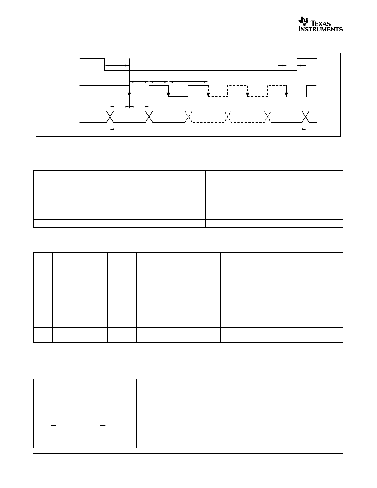
t
SLOADS
t
WSCLK
t
OS
t
OH
t
WSCLK
t
SCLK
16 x M
MSB LSB LSBMSB
t
SLOADH
SCLK
SEN
SDATA
V
DFS
2
12
AV
DD
4
12
AVDD V
DFS
5
12
AV
DD
7
12
AVDD V
DFS
8
12
AV
DD
V
DFS
10
12
AV
DD
ADS5521
SBAS309A – MAY 2004 – REVISED APRIL 2005
Figure 4. Serial Programming Interface Timing Diagram
Table 1. Serial Programming Interface TIming Characteristics
SYMBOL PARAMETER MIN
t
SCLK
t
WSCLK
t
SLOADS
t
SLOADH
t
DS
t
DH
(1) Typ, min, and max values are characterized, but not production tested.
SCLK period 50 ns
SCLK duty cycle 25 50 75 %
SEN to SCLK setup time 8 ns
SCLK to SEN hold time 6 ns
Data setup time 8 ns
Data hold time 6 ns
(1)
(1)
TYP
(1)
MAX
UNIT
Table 2. Serial Register Table
A3 A2 A1 A0 D11 D10 D9 D8 D7 D6 D5 D4 D3 D2 D1 D0 DESCRIPTION
1 1 0 1 0 0 0 0 0 0 0 0 0 0 DLL 0 DLL OFF = 0: Internal DLL is on; recommended for 60MSPS
OFF to 105MSPS clock speeds.
1 1 1 0 0 TP<1> TP<0> 0 0 0 0 0 0 0 0 0 TP<1:0> - Test modes for output data capture
1 1 1 1 PDN 0 0 0 0 0 0 0 0 0 0 0 PDN = 0: Normal mode of operation
(1)
DLL OFF = 1: Internal DLL is off; recommended for 2MSPS to
80MSPS clock speeds.
TP<1:0> = 00: Normal mode of operation
TP<1:0> = 01: All outputs forced to 0
TP<1:0> = 10: All outputs forced to 1
TP<1:0> = 11: Each output bit toggles between 0 and 1.
There is no ensured relationship between the bits.
PDN = 1: Device is put in power-down (low-current) mode.
(1) All register contents default to zero on reset.
(2) The patterns given are applicable to the straight offset binary output format. If two's complement output format is selected, the test mode
outputs will be the binary two's complement equivalent of these patterns.
Table 3. Data Format Select (DFS) Table
DFS-PIN VOLTAGE (V
) DATA FORMAT CLOCK OUTPUT POLARITY
DFS
Straight Binary Data valid on rising edge
Two's Complement Data valid on rising edge
Straight Binary Data valid on falling edge
(2)
8
Two's Complement Data valid on falling edge
Page 9
www.ti.com
48
47
46
45
44
43
42
41
40
39
38
37
36
35
34
33
DR
GND
D1
D0 (LSB)
NC
NC
CLKOUT
DR
GND
OE
DFS
AV
DD
A
GND
AV
DD
A
GND
RESET
AV
DD
AV
DD
1
2
3
4
5
6
7
8
9
10
11
12
13
14
15
16
DR
GND
SCLK
SDATA
SEN
AV
DD
A
GND
AV
DD
A
GND
AV
DD
CLKP
CLKM
A
GND
A
GND
A
GND
AV
DD
A
GND
OVR
D11 (MSB)
D10
D9
D8
DR
GND
DRV
DD
DR
GND
D7
D6
D5
D4
D3
D2
DR
GND
DRV
DD
CM
A
GND
INP
INM
A
GND
AV
DD
A
GND
AV
DD
A
GND
AV
DD
A
GND
AV
DD
REFP
REFM
IREF
A
GND
64 63 62 61 60 59 58 57 56 55 54
17 18 19 20 21 22 23 24 25 26 27
53 52 51 50 49
28 29 30 31 32
PowerPAD
(Connected to Analog Ground)
ADS5521
ADS5521
SBAS309A – MAY 2004 – REVISED APRIL 2005
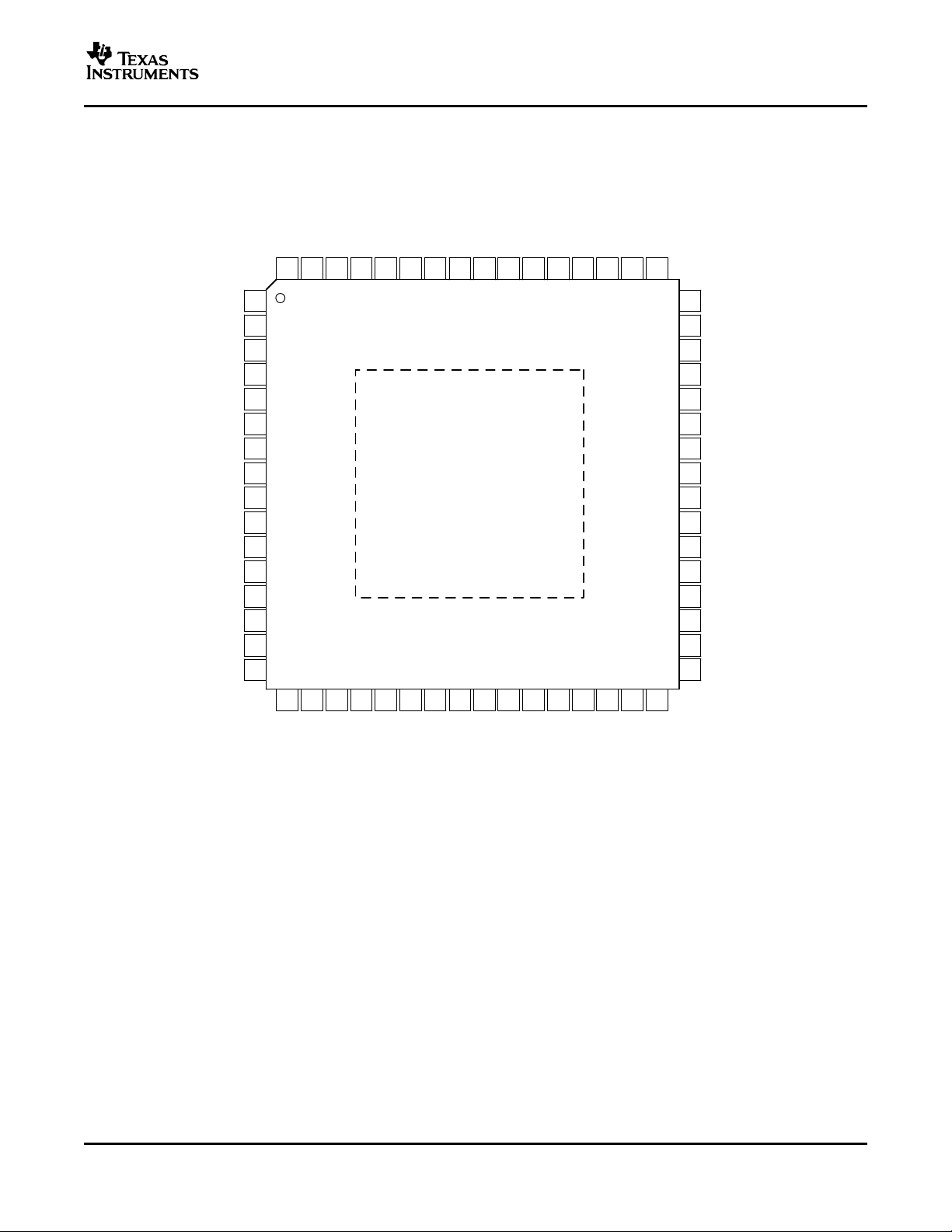
PIN CONFIGURATION
PAP PACKAGE
HTQFP-64
(TOP VIEW)
9
Page 10

www.ti.com
ADS5521
SBAS309A – MAY 2004 – REVISED APRIL 2005
PIN CONFIGURATION (continued)
PIN ASSIGNMENTS
TERMINAL
NAME NO. PINS I/O DESCRIPTION
5, 7, 9, 15, 22,
AV
DD
24, 26, 28, 33, 12 I Analog power supply
34, 37, 39
6, 8, 12, 13,
A
GND
14, 16, 18, 21,
23, 25, 27, 32,
36, 38
DRV
DD
DR
GND
49, 58 2 I Output driver power supply
1, 42, 48, 50,
57, 59
NC 44, 45 2 — Not connected
INP 19 1 I Differential analog input (positive)
INM 20 1 I Differential analog input (negative)
REFP 29 1 O Reference voltage (positive); 0.1µF capacitor in series with a 1 Ω resistor to GND
REFM 30 1 O Reference voltage (negative); 0.1µF capacitor in series with a 1 Ω resistor to GND
IREF 31 1 I Current set; 56k Ω resistor to GND; do not connect capacitors
CM 17 1 O Common-mode output voltage
RESET 35 1 I Reset (active high), 200k Ω resistor to AV
OE 41 1 I Output enable (active high)
DFS 40 1 I Data format and clock out polarity select
CLKP 10 1 I Data converter differential input clock (positive)
CLKM 11 1 I Data converter differential input clock (negative)
SEN 4 1 I Serial interface chip select
SDATA 3 1 I Serial interface data
SCLK 2 1 I Serial interface clock
D0 (LSB) to 46, 47, 51-56,
D11 (MSB) 60-63
OVR 64 1 O Over-range indicator bit
CLKOUT 43 1 O CMOS clock out in sync with data
(1) PowerPAD is connected to analog ground.
(2) Table 3 defines the voltage levels for each mode selectable via the DFS pin.
NO. OF
14 I Analog ground
6 I Output driver ground
14 O Parallel data output
(1)
DD
(2)
10
Page 11

www.ti.com
DEFINITION OF SPECIFICATIONS
SNR 10Log
10
P
S
P
N
SINAD 10Log
10
P
S
PN P
D
ENOB
SINAD 1.76
6.02
Analog Bandwidth
The analog input frequency at which the power of the
fundamental is reduced by 3dB with respect to the
low frequency value.
Aperture Delay
The delay in time between the falling edge of the
input sampling clock and the actual time at which the
sampling occurs.
Aperture Uncertainty (Jitter)
The sample-to-sample variation in aperture delay.
Clock Pulse Width/Duty Cycle
The duty cycle of a clock signal is the ratio of the time
the clock signal remains at a logic high (clock pulse
width) to the period of the clock signal. Duty cycle is
typically expressed as a percentage. A perfect differential sine wave clock results in a 50% duty cycle.
Maximum Conversion Rate
The maximum sampling rate at which certified operation is given. All parametric testing is performed at
this sampling rate unless otherwise noted.
Minimum Conversion Rate
The minimum sampling rate at which the ADC functions.
Differential Nonlinearity (DNL)
An ideal ADC exhibits code transitions at analog input
values spaced exactly 1LSB apart. The DNL is the
deviation of any single step from this ideal value,
measured in units of LSBs.
Integral Nonlinearity (INL)
The INL is the deviation of the ADC's transfer
function from a best fit line determined by a least
squares curve fit of that transfer function, measured
in units of LSBs.
Gain Error
The gain error is the deviation of the ADC's actual
input full-scale range from its ideal value. The gain
error is given as a percentage of the ideal input
full-scale range. Gain error does not account for
variations in the internal reference voltages (see the
Electrical Specifications section for limits on the
variation of V
and V
REFP
).
REFM
ADS5521
SBAS309A – MAY 2004 – REVISED APRIL 2005
Offset Error
The offset error is the difference, given in number of
LSBs, between the ADC's actual average idle channel output code and the ideal average idle channel
output code. This quantity is often mapped into mV.
Temperature Drift
The temperature drift coefficient (with respect to gain
error and offset error) specifies the change per
degree Celsius of the parameter from T
is calculated by dividing the maximum deviation of
the parameter across the T
difference (T
– T
MAX
).
MIN
to T
MIN
MAX
Signal-to-Noise Ratio (SNR)
SNR is the ratio of the power of the fundamental (P
to the noise floor power (P
), excluding the power at
N
DC and the first eight harmonics.
SNR is either given in units of dBc (dB to carrier)
when the absolute power of the fundamental is used
as the reference, or dBFS (dB to Full-Scale) when the
power of the fundamental is extrapolated to the
converter's full-scale range.
Signal-to-Noise and Distortion (SINAD)
SINAD is the ratio of the power of the fundamental
(P
) to the power of all the other spectral components
S
including noise (P
) and distortion (P
N
DC.
SINAD is either given in units of dBc (dB to carrier)
when the absolute power of the fundamental is used
as the reference, or dBFS (dB to Full-Scale) when the
power of the fundamental is extrapolated to the
converter's full-scale range.
Effective Number of Bits (ENOB)
The ENOB is a measure of a converter's performance
as compared to the theoretical limit based on
quantization noise.
), but excluding
D
to T
MIN
range by the
MAX
. It
)
S
11
Page 12

www.ti.com
THD 10Log
10
P
S
P
D
ADS5521
SBAS309A – MAY 2004 – REVISED APRIL 2005
Total Harmonic Distortion (THD) Two-Tone Intermodulation Distortion (IMD3)
THD is the ratio of the power of the fundamental (P
to the power of the first eight harmonics (P
). frequencies f1and f2) to the power of the worst
D
THD is typically given in units of dBc (dB to carrier).
Spurious-Free Dynamic Range (SFDR)
The ratio of the power of the fundamental to the
highest other spectral component (either spur or
harmonic). SFDR is typically given in units of dBc (dB
to carrier).
) IMD3 is the ratio of the power of the fundamental (at
S
spectral component at either frequency 2f
2f
– f1. IMD3 is either given in units of dBc (dB to
2
carrier) when the absolute power of the fundamental
is used as the reference, or dBFS (dB to Full-Scale)
when the power of the fundamental is extrapolated to
the converter's full-scale range.
– f2or
1
12
Page 13

www.ti.com
0
−
20
−
40
−
60
−
80
−
100
−
120
Magnitude
−
dB
f−Frequency−MHz
0 10 20 30 40 50
52.5
SFDR = 92.6dBc
SNR = 71.3dBFS
THD = 88.2dBc
SINAD = 71.2dBFS
0
−
20
−
40
−
60
−
80
−
100
−
120
Magnitude
−
dB
f−Frequency−MHz
0 10 20 30 40 50
52.5
SFDR = 88.9dBc
SNR = 71.1dBFS
THD = 86.9dBc
SINAD = 71.0dBFS
0
−
20
−
40
−
60
−
80
−
100
−
120
Magnitude
−
dB
f−Frequency−MHz
0 10 20 30 40 50
52.5
SFDR = 90.4dBc
SNR = 71.0dBFS
THD = 85.4dBc
SINAD = 70.8dBFS
0
−
20
−
40
−
60
−
80
−
100
−
120
Magnitude
−
dB
f−Frequency−MHz
0 10 20 30 40 50
52.5
SFDR = 81.7dBc
SNR = 70.6dBFS
THD = 80.3dBc
SINAD = 70.2dBFS
0
−
20
−
40
−
60
−
80
−
100
−
120
Magnitude
−
dB
f−Frequency−MHz
0 10 20 30 40 50
52.5
SFDR = 84.5dBc
SNR = 70.4dBFS
THD = 83.3dBc
SINAD = 70.2dBFS
0
−
20
−
40
−
60
−
80
−
100
−
120
Magnitude
−
dB
f−Frequency−MHz
0 10 20 30 40 50
52.5
SFDR = 86.2dBc
SNR = 70.1dBFS
THD = 85.2dBc
SINAD = 70.0dBFS
Typical values given at TA= +25 ° C, AV
3V
differential clock, and –1dBFS differential input, unless otherwise noted.
PP
SPECTRAL PERFORMANCE SPECTRAL PERFORMANCE
(FFT for 4MHz Input Signal) (FFT for 16MHz Input Signal)
Figure 5. Figure 6.
ADS5521
SBAS309A – MAY 2004 – REVISED APRIL 2005
TYPICAL CHARACTERISTICS
= DRV
DD
= 3.3V, sampling rate = 105MSPS, 50% clock duty cycle, DLL On,
DD
SPECTRAL PERFORMANCE SPECTRAL PERFORMANCE
(FFT for 55MHz Input Signal) (FFT for 70MHz Input Signal)
Figure 7. Figure 8.
SPECTRAL PERFORMANCE SPECTRAL PERFORMANCE
(FFT for 80MHz Input Signal) (FFT for 100MHz Input Signal)
Figure 9. Figure 10.
13
Page 14

www.ti.com
0
−
20
−
40
−
60
−
80
−
100
−
120
Magnitude
−
dB
f−Frequency−MHz
0 10 20 30 40 50
52.5
SFDR = 75.3dBc
SNR = 69.4dBFS
THD = 75.0dBc
SINAD = 68.1dBFS
0
−
20
−
40
−
60
−
80
−
100
−
120
Magnitude
−
dB
f−Frequency−MHz
0 10 20 30 40 50
52.5
SFDR = 73.1dBc
SNR = 68.2dBFS
THD = 71.9dBc
SINAD = 66.6dBFS
0
−
20
−
40
−
60
−
80
−
100
−
120
Magnitude
−
dB
f−Frequency−MHz
0 10 20 30 40 50
52.5
SFDR = 65.6dBc
SNR = 66.6dBFS
THD = 64.9dBc
SINAD = 62.7dBFS
f1 = 10.1MHz (−7dBFS)
f2 = 15.1MHz (−7dBFS)
2−Tone IMD = 94.1dBFS
0
−
20
−
40
−
60
−
80
−
100
−
120
Magnitude
−
dB
f−Frequency−MHz
0 10 20 30 40 50
52.5
f1 = 45.1MHz (−7dBFS)
f2 = 50.1MHz (−7dBFS)
2−Tone IMD = 94.0dBc
0
−
20
−
40
−
60
−
80
−
100
−
120
Magnitude
−
dB
f−Frequency−MHz
0 10 20 30 40 50
52.5
0
−
20
−
40
−
60
−
80
−
100
−
120
Magnitude
−
dB
f−Frequency−MHz
0 10 20 30 40 50
52.5
0
f1 = 150.1MHz (−7dBFS)
f2 = 155.1MHz (−7dBFS)
2−Tone IMD = 85.1dBFS
ADS5521
SBAS309A – MAY 2004 – REVISED APRIL 2005
TYPICAL CHARACTERISTICS (continued)
Typical values given at TA= +25 ° C, AV
3V
differential clock, and –1dBFS differential input, unless otherwise noted.
PP
SPECTRAL PERFORMANCE SPECTRAL PERFORMANCE
(FFT for 150MHz Input Signal) (FFT for 220MHz Input Signal)
= DRV
DD
= 3.3V, sampling rate = 105MSPS, 50% clock duty cycle, DLL On,
DD
Figure 11. Figure 12.
SPECTRAL PERFORMANCE TWO-TONE
(FFT for 300MHz Input Signal) INTERMODULATION
Figure 13. Figure 14.
TWO-TONE TWO-TONE
INTERMODULATION INTERMODULATION
14
Figure 15. Figure 16.
Page 15

www.ti.com
0.25
0.20
0.15
0.10
0.05
0
−
0.05
−
0.10
−
0.15
−
0.20
−
0.25
DNL
−
LSB
Code
0 1024 30722048 4096
fIN= 10MHz
AIN=−0.5dBFS
1.0
0.8
0.6
0.4
0.2
0
−
0.2
−
0.4
−
0.6
−
0.8
−
1.0
INL
−
LSB
Code
0 1024 30722048 4096
fIN= 10MHz
AIN=−0.5dBFS
95
90
85
80
75
70
65
60
0 50 100 150 200 250 300
Frequency−MHz
SFDR
−
dBc
76
74
72
70
68
66
64
62
60
0 50 100 150 200 250 300
Frequency−MHz
SNR
−
dBFS
76
75
74
73
72
71
70
69
68
3.0 3.1 3.2 3.3 3.4 3.5 3.6
fIN= 150MHz
SFDR
AV
DD
−
Analog Supply Voltage−V
SFDR
−
dBcSNR
−
dBFS
SNR
95
90
85
80
75
70
65
60
AV
DD
−
Analog Supply Voltage−V
3.0 3.1 3.2 3.3 3.4 3.5 3.6
fIN= 70MHz
SFDR
SNR
SFDR
−
dBcSNR
−
dBFS
TYPICAL CHARACTERISTICS (continued)
Typical values given at TA= +25 ° C, AV
3V
differential clock, and –1dBFS differential input, unless otherwise noted.
PP
DIFFERENTIAL INTEGRAL
NONLINEARITY NONLINEARITY
Figure 17. Figure 18.
= DRV
DD
= 3.3V, sampling rate = 105MSPS, 50% clock duty cycle, DLL On,
DD
ADS5521
SBAS309A – MAY 2004 – REVISED APRIL 2005
SPURIOUS-FREE DYNAMIC RANGE SIGNAL-TO-NOISE RATIO
vs INPUT FREQUENCY vs INPUT FREQUENCY
Figure 19. Figure 20.
AC PERFORMANCE AC PERFORMANCE
vs ANALOG SUPPLY VOLTAGE vs ANALOG SUPPLY VOLTAGE
Figure 21. Figure 22.
15
Page 16

www.ti.com
78
76
74
72
70
68
66
DV
DD
−
Digital Supply Voltage−V
3.0 3.1 3.2 3.3 3.4 3.5 3.6
fIN= 150MHz
SFDR
SNR
SFDR
−
dBcSNR
−
dBFS
88
84
80
76
72
68
64
DV
DD
−
Digital Supply Voltage−V
3.0 3.1 3.2 3.3 3.4 3.5 3.6
fIN= 70MHz
SFDR
SNR
SFDR
−
dBcSNR
−
dBFS
800
750
700
650
600
550
500
450
Power Dissipation
−
mW
Sample Rate−MSPS
10 20 30 40 50 60 70 80 90 100
105
fIN= 150MHz
DLL On
DLL Off
800
750
700
650
600
550
500
450
Power Dissipation
−
mW
fIN= 70MHz
Sample Rate−MSPS
10 20 30 40 50 60 70 80 90 100
105
DLL On
DLL Off
90
85
80
75
70
65
60
−
40
−
15 +85+60+35+10
Temperature
−
C
SNR
−
dBFS SFDR
−
dBc
fIN= 70MHz
SFDR
SNR
90
80
70
60
50
40
30
20
10
0
−
10
−
20
−
30
AC Performance
−
dB
Input Amplitude−dBFS
−
100−90−80−70−60−50−40−30−20−10 0
fIN= 70MHz
SFDR (dBc)
SNR (dBc)
SNR (dBFS)
ADS5521
SBAS309A – MAY 2004 – REVISED APRIL 2005
TYPICAL CHARACTERISTICS (continued)
Typical values given at TA= +25 ° C, AV
3V
differential clock, and –1dBFS differential input, unless otherwise noted.
PP
AC PERFORMANCE AC PERFORMANCE
vs DIGITAL SUPPLY VOLTAGE vs DIGITAL SUPPLY VOLTAGE
= DRV
DD
= 3.3V, sampling rate = 105MSPS, 50% clock duty cycle, DLL On,
DD
Figure 23. Figure 24.
POWER DISSIPATION POWER DISSIPATION
vs SAMPLE RATE vs SAMPLE RATE
Figure 25. Figure 26.
AC PERFORMANCE AC PERFORMANCE
vs TEMPERATURE vs INPUT AMPLITUDE
16
Figure 27. Figure 28.
Page 17

www.ti.com
100
90
80
70
60
50
40
30
20
10
0
−
10
−
20
−
30
AC Performance
−
dB
Input Amplitude−dBFS
−
100−90−80−70−60−50−40−30−20−10 0
fIN= 150MHz
SFDR (dBc)
SNR (dBc)
SNR (dBFS)
90
80
70
60
50
40
30
20
10
0
−
10
−
20
−
30
AC Performance
−
dB
Input Amplitude−dBFS
−
100−90−80−70−60−50−40−30−20−10 0
fIN= 220MHz
SFDR (dBc)
SNR (dBc)
SNR (dBFS)
95
90
85
80
75
70
65
60
Differential Clock Amplitude−V
0 0.5 1.0 1.5 2.0 2.5 3.0
fIN= 70MHz
SFDR
SNR
SFDR
−
dBcSNR
−
dBFS
100
90
80
70
60
50
40
30
20
10
0
2045
2046
2047
2048
2049
2050
2051
2052
2053
2054
2055
2056
2057
2058
2059
Occurrence
−
%
Code
0
−
20
−
40
−
60
−
80
−
100
−
120
−
140
Magnitude
−
dB
f−Frequency−MHz
0 5 10 15 20 25 30 35 40 45 50
fS= 92.16MSPS
fIN= 170MHz
100
95
90
85
80
75
70
65
60
Clock Duty Cycle−%
35 40 5045 55 6560
SFDR
SNR
SFDR
−
dBcSNR
−
dBFS
fIN= 20MHz
TYPICAL CHARACTERISTICS (continued)
Typical values given at TA= +25 ° C, AV
3V
differential clock, and –1dBFS differential input, unless otherwise noted.
PP
AC PERFORMANCE AC PERFORMANCE
vs INPUT AMPLITUDE vs INPUT AMPLITUDE
= DRV
DD
= 3.3V, sampling rate = 105MSPS, 50% clock duty cycle, DLL On,
DD
ADS5521
SBAS309A – MAY 2004 – REVISED APRIL 2005
Figure 29. Figure 30.
OUTPUT AC PERFORMANCE
NOISE HISTOGRAM vs CLOCK AMPLITUDE
Figure 31. Figure 32.
WCDMA AC PERFORMANCE
CARRIER vs CLOCK DUTY CYCLE
Figure 33. Figure 34.
17
Page 18

www.ti.com
Input Frequency−MHz
Sample Rate
−
MSPS
20 40 60 80 100 120 140 160 180 200 220
65
70
75
80
85
90
95
100
105
110
115
120
125
67.5
68
68.5
69
69.5
70
70.5
71
SNR
−
dBFS
71
71
71
71
71.5
68.5
68.5
68
70.5
70.5
70.5
70.5
70
70
70
70.5
70.5
69.5
69.5
69.5
69
69
69
Input Frequency−MHz
Sampe Rate
−
MSPS
SNR
−
dBFS
62
64
66
68
71
70
69
67
65
63
20 40 60 80 100 120 140 160 180 200 220
10
20
30
40
50
60
70
80
90
100
61
63
61
71
71
71
71
62
63
63
64
64
65
65
66
66
66
67
67
67
68
68
68
68
69
69
69
69
69
70
70
70
70
60
ADS5521
SBAS309A – MAY 2004 – REVISED APRIL 2005
Typical values given at TA= +25°C, AV
3V
PP
TYPICAL CHARACTERISTICS
= DRV
DD
differential clock, and –1dBFS differential input, unless otherwise noted.
SIGNAL-TO-NOISE RATIO (SNR)
= 3.3V, sampling rate = 105MSPS, 50% clock duty cycle,
DD
(DLL On)
Figure 35.
SIGNAL-TO-NOISE RATIO (SNR)
(DLL Off)
Figure 36.
18
Page 19

www.ti.com
Input Frequency−MHz
Sample Rate
−
MSPS
SFDR
−
dBc
20 40 60 80 100 120 140 160 180 200 220
125
120
115
110
105
100
95
90
85
80
75
70
65
90
85
80
75
70
73
75
75
91
89
89
89
89
89
91
93
75
75
77
77
77
77
77
79
79
79
79
79
79
79
81
81
81
81
81
81
81
81
81
83
83
85
85
85
85
85
85
85
87
87
87
87
87
87
83
83
83
83
100
90
80
70
60
50
40
30
20
10
90
88
86
84
82
80
78
76
74
72
70
68
66
64
Input Frequency−MHz
140 160120 180 200 22020 40 60 80 100
Sample Rate
−
MSPS
SFDR
−
dBc
66
66
86
86
86
86
86
86
88
90
90
88
88
88
88
88
88
88
86
86
86
86
7072
72
72
70
70
66
68
68
68
64
78
78
78
78
80
80
80
80
80
82
82
82
82
82
84
84
84
84
84
84
84
84
84
84
74
74
74
76
76
76
86
86
86
TYPICAL CHARACTERISTICS (continued)
Typical values given at TA= +25°C, AV
3V
differential clock, and –1dBFS differential input, unless otherwise noted.
PP
= DRV
DD
= 3.3V, sampling rate = 105MSPS, 50% clock duty cycle,
DD
SPURIOUS-FREE DYNAMIC RANGE (SFDR)
ADS5521
SBAS309A – MAY 2004 – REVISED APRIL 2005
(DLL On)
Figure 37.
SPURIOUS-FREE DYNAMIC RANGE (SFDR)
(DLL Off)
Figure 38.
19
Page 20

www.ti.com
R
3
R
1a
L
1
L1, L2: 6nH−10nH effective
R1a, R1b: 5Ω−8
Ω
C1a, C1b: 2.2pF−2.6pF
CP1, CP2: 2.5pF−3.5pF
CP3, CP4, : 1.2pF−1.8pF
CA: 0.8pF−1.2pF
R3: 80Ωto 120
Ω
Switches:
S1a, S1b: On Resistance: 35Ω−50
Ω
S2: On Resistance: 7.5Ω−15
Ω
S3a, S3b: On Resistance: 40Ω−60
Ω
All switches Off Resistance: 10G
Ω
L
2
R
1b
C
1a
S
1a
S
1b
S
3a
S
3b
S
2
C
1b
C
A
CP
1
CP
3
VINCM
1V
CP
4
CP
2
INP
INM
ADS5521
SBAS309A – MAY 2004 – REVISED APRIL 2005
APPLICATION INFORMATION
gate the sample through the pipeline every half clock
THEORY OF OPERATION
The ADS5521 is a low-power, 12-bit, 105MSPS,
CMOS, switched capacitor, pipeline ADC that
operates from a single 3.3V supply. The conversion
process is initiated by a falling edge of the external
input clock. Once the signal is captured by the input
S&H, the input sample is sequentially converted by a The analog input for the ADS5521 consists of a
series of small resolution stages, with the outputs differential sample-and-hold architecture implemented
combined in a digital correction logic block. Both the using a switched capacitor technique, shown in Fig-
rising and the falling clock edges are used to propa- ure 39 .
cycle. This process results in a data latency of 16.5
clock cycles, after which the output data is available
as a 12-bit parallel word, coded in either straight
offset binary or binary two's complement format.
INPUT CONFIGURATION
20
Figure 39. Analog Input Stage
Page 21

www.ti.com
500A fS(in MSPS)
105 MSPS
R
0
50
Ω
Z
0
50
Ω
1:1
INP
ADS5521
INM
CM
ADT1−1WT
R
50
Ω
1nF 0.1µF
AC Signal
Source
10
Ω
25
Ω
25
Ω
ADS5521
SBAS309A – MAY 2004 – REVISED APRIL 2005
This differential input topology produces a high level Since the input signal must be biased around the
of AC performance for high sampling rates. It also common-mode voltage of the internal circuitry, the
results in a very high usable input bandwidth, es- common-mode voltage (V
pecially important for high intermediate-frequency (IF) connected to the center-tap of the secondary winding.
or undersampling applications. The ADS5521 requires each of the analog inputs (INP, INM) to be
externally biased around the common-mode level of
the internal circuitry (CM, pin 17). For a full-scale
differential input, each of the differential lines of the
input signal (pins 19 and 20) swings symmetrically
between CM + 0.575V and CM – 0.575V. This means
that each input is driven with a signal of up to CM ±
0.575V, so that each input has a maximum differential signal of 1.15V
swing of 2.3V
PP
for a total differential input signal
PP
. The maximum swing is determined
by the two reference voltages, the top reference
(REFP, pin 29), and the bottom reference (REFM, pin
To ensure a steady low-noise V
performance is attained when the CM output (pin 17)
is filtered to ground with a 10 Ω series resistor and
parallel 0.1µF and 0.001µF low-inductance capacitors, as illustrated in Figure 39 .
Output V
(pin 17) is designed to directly drive the
CM
ADC input. When providing a custom CM level, be
aware that the input structure of the ADC sinks a
common-mode current in the order of 500µA (250µA
per input). Equation 1 describes the dependency of
the common-mode current and the sampling frequency:
30).
The ADS5521 obtains optimum performance when
the analog inputs are driven differentially. The circuit
shown in Figure 40 illustrates one possible configuration using an RF transformer.
Where:
fS> 2MSPS.
This equation helps to design the output capability
and impedance of the driving circuit accordingly.
When it is necessary to buffer or apply a gain to the
incoming analog signal, it is possible to combine
single-ended operational amplifiers with an RF transformer, or to use a differential input/output amplifier
without a transformer, to drive the input of the
ADS5521. TI offers a wide selection of single-ended
operational amplifiers (including the THS3201,
THS3202, OPA695, and OPA847) that can be selected depending on the application. An RF gain block
amplifier, such as TI's THS9001, can also be used
with an RF transformer for very high input frequency
Figure 40. Transformer Input to Convert
Single-Ended Signal to Differential Signal
applications. The THS4503 is a recommended differential input/output amplifier. Table 4 lists the recommended amplifiers.
The single-ended signal is fed to the primary winding
of an RF transformer. Placing a 25 Ω resistor in series
with INP and INM is recommended to dampen ringing
due to ADC kickback.
) from the ADS5521 is
CM
reference, best
CM
(1)
INPUT SIGNAL FREQUENCY RECOMMENDED AMPLIFIER TYPE OF AMPLIFIER USE WITH TRANSFORMER?
10MHz to 120MHz THS3201 Operational Amp Yes
Over 100MHz THS9001 RF Gain Block Yes
Table 4. Recommended Amplifiers to Drive the Input of the ADS5521
DC to 20MHz THS4503 Differential In/Out Amp No
DC to 50MHz OPA847 Operational Amp Yes
OPA695 Operational Amp Yes
THS3202 Operational Amp Yes
21
Page 22

www.ti.com
R
IN
R
IN
C
IN
0.1µF
R
T
100
Ω
0.1µF
1000pF
1:1
R
S
100
Ω
OPA695
R
1
400
Ω
AV= 8V/V
(18dB)
R
2
57.5
Ω
V
IN
ADS5521
INP
INM
CM
−
5V+5V
10
Ω
R
F
R
G
V
OCM
INP
INM
CM
R
F
R
G
R
S
ADS5521
12−Bit/105MSPS
0.1µF
0.1µF
10µF
1µF
R
T
+3.3V
+5V
0.1µF10µF
−
5V
THS4503
R
IN
R
IN
10
Ω
ADS5521
SBAS309A – MAY 2004 – REVISED APRIL 2005
When using single-ended operational amplifiers (such that these components be included in the ADS5521
as the THS3201, THS3202, OPA695, or OPA847) to circuit layout when any of the amplifier circuits disprovide gain, a three-amplifier circuit is recommended cussed previously are used. The components allow
with one amplifier driving the primary of an RF fine-tuning of the circuit performance. Any mismatch
transformer and one amplifier in each of the legs of between the differential lines of the ADS5521 input
the secondary driving the two differential inputs of the produces a degradation in performance at high input
ADS5521. These three amplifier circuits minimize frequencies, mainly characterized by an increase in
even-order harmonics. For very high frequency in- the even-order harmonics. In this case, special care
puts, an RF gain block amplifier can be used to drive should be taken to keep as much electrical symmetry
a transformer primary; in this case, the transformer as possible between both inputs.
secondary connections can drive the input of the
ADS5521 directly, as shown in Figure 40 , or with the
addition of the filter circuit shown in Figure 41 .
Figure 41 illustrates how R
and C
IN
can be placed requiring DC coupling of the input. Flexible in their
IN
to isolate the signal source from the switching inputs configurations (see Figure 42 ), such amplifiers can be
of the ADC and to implement a low-pass RC filter to used for single-ended-to-differential conversion signal
limit the input noise in the ADC. It is recommended amplification.
Another possible configuration for lower-frequency
signals is the use of differential input/output amplifiers
that can simplify the driver circuit for applications
Figure 41. Converting a Single-Ended Input Signal to a Differential Signal Using an RF Transformer
22
Figure 42. Using the THS4503 with the ADS5521
Page 23

www.ti.com
29
30
31
REFP
REFM
IREF
56k
Ω
1µF
1µF
1
Ω
1
Ω
ADS5521
SBAS309A – MAY 2004 – REVISED APRIL 2005
INPUT VOLTAGE OVER-STRESS
The ADS5521 can handle absolute maximum voltages of 3.6V DC on the input pins INP and INM. For
DC inputs between 3.6V and 3.8V, a 25 Ω resistor is
required in series with the input pins. For inputs
above 3.8V, the device can handle only transients,
which need to have less than 5% duty cycle of
overstress. The input pins connect internally to an
ESD diode to AV
circuit. The sampling capacitor of the switched capacitor circuit connects to the input pins through a
switch in the sample phase. In this phase, an input
larger than 2.65V would cause the switched capacitor
circuit to present an equivalent load of a forward
biased diode to 2.65V, in series with a 60 Ω impedance. Also, beyond the voltage on AV
diode to AV
DD
In the phase where the sampling switch is off, the
diode loading from the input switched capacitor circuit
is disconnected from the pin, while the ESD loading
to AV
is still present.
DD
A violation of any of the previously stated
conditions could damage the device (or reduce its lifetime) either due to
electromigration or gate oxide integrity. Care
should be taken not to expose the device to
input over-voltage for extended periods of
time as it may degrade device reliability.
, as well as a switched capacitor
DD
starts to become forward biased.
CAUTION:
, the ESD
DD
The device can be powered down by programming
the internal register (see Serial Programming
Interface section). The outputs become tri-stated and
only the internal reference is powered up to shorten
the power-up time. The Power-Down mode reduces
power dissipation to a minimum of 180mW.
REFERENCE CIRCUIT
The ADS5521 has built-in internal reference generation, requiring no external circuitry on the printed
circuit board (PCB). For optimum performance, it is
best to connect both REFP and REFM to ground with
a 1µF decoupling capacitor in series with a 1 Ω
resistor, as shown in Figure 43 . In addition, an
external 56.2k Ω resistor should be connected from
IREF (pin 31) to AGND to set the proper current for
the operation of the ADC, as shown in Figure 43 . No
capacitor should be connected between pin 31 and
ground; only the 56.2k Ω resistor should be used.
POWER-SUPPLY SEQUENCE
The preferred mode of power-supply sequencing is to
power-up AV
first, followed by DRV
DD
DD
. Raising both
supplies simultaneously is also a valid power supply
sequence. In the event that DRV
AV
in the system, AV
DD
of DRV
.
DD
must power up within 10ms
DD
DD
powers up before
POWER-DOWN
The device will enter power-down mode in one of two
ways: either by reducing the clock speed to between
DC and 1MHz, or by setting a bit through the serial
programming interface. If reducing the clock speed,
power-down may be initiated for any clock frequency
below 10MHz. The actual frequency at which the
device powers down varies from device to device.
Figure 43. REFP, REFM, and IREF Connections
for Optimum Performance
CLOCK INPUT
The ADS5521 clock input can be driven with either a
differential clock signal or a single-ended clock input,
with little or no difference in performance between
both configurations. The common-mode voltage of
the clock inputs is set internally to CM (pin 17) using
internal 5k Ω resistors that connect CLKP (pin 10) and
CLKM (pin 11) to CM (pin 17), as shown in Figure 44 .
23
Page 24

www.ti.com
5k
Ω
5k
Ω
CLKMCLKP
CM CM
6pF
3pF3pF
100
95
90
85
80
75
70
65
60
Clock Duty Cycle−%
35 40 5045 55 6560
SFDR
SNR
SFDR
−
dBcSNR
−
dBFS
fIN= 20MHz
0.01µF
0.01µF
CLKP
ADS5521
CLKM
Square Wave
or Sine Wave
(3VPP)
0.01µF
CLKP
ADS5521
CLKM
0.01µF
Differential Square Wave
or Sine Wave
(3VPP)
95
90
85
80
75
70
65
60
Differential Clock Amplitude−V
0 0.5 1.0 1.5 2.0 2.5 3.0
fIN= 70MHz
SFDR
SNR
SFDR
−
dBcSNR
−
dBFS
ADS5521
SBAS309A – MAY 2004 – REVISED APRIL 2005
Figure 44. Clock Inputs
When driven with a single-ended CMOS clock input,
it is best to connect CLKM (pin 11) to ground with a
0.01µF capacitor, while CLKP is AC-coupled with a
0.01µF capacitor to the clock source, as shown in
Figure 45 .
For high input frequency sampling, it is recommended
to use a clock source with very low jitter. Additionally,
the internal ADC core uses both edges of the clock
for the conversion process. This means that, ideally,
a 50% duty cycle should be provided. Figure 47
shows the performance variation of the ADC versus
clock duty cycle.
Figure 47. AC Performance vs Clock Duty Cycle
Figure 45. AC-Coupled, Single-Ended Clock Input
The ADS5521 clock input can also be driven differentially, reducing susceptibility to common-mode noise.
In this case, it is best to connect both clock inputs to
the differential input clock signal with 0.01µF capacitors, as shown in Figure 46 .
Figure 46. AC-Coupled, Differential Clock Input
24
Bandpass filtering of the source can help produce a
50% duty cycle clock and reduce the effect of jitter.
When using a sinusoidal clock, the clock jitter will
further improve as the amplitude is increased. In that
sense, using a differential clock allows for the use of
larger amplitudes without exceeding the supply rails
and absolute maximum ratings of the ADC clock
input. Figure 48 shows the performance variation of
the device versus input clock amplitude. For detailed
clocking schemes based on transformer or
PECL-level clocks, refer to the ADS55xxEVM User's
Guide (SLWU010 ), available for download from
www.ti.com.
Figure 48. AC Performance vs Clock Amplitude
Page 25

www.ti.com
ADS5521
SBAS309A – MAY 2004 – REVISED APRIL 2005
INTERNAL DLL
In order to obtain the fastest sampling rates achievable with the ADS5521, the device uses an internal
digital phase lock loop (DLL). Nevertheless, the
limited frequency range of operation of DLL degrades
two's complement output format. For a negative input
overdrive, the output code is 0x000 in straight offset
binary output format, and 0x800 in two's complement
output format. These outputs to an overdrive signal
are ensured through design and characterization.
the performance at clock frequencies below 60MSPS. The output circuitry of the ADS5521, by design,
In order to operate the device below 60MSPS, the minimizes the noise produced by the data switching
internal DLL must be shut off using the DLL OFF transients, and, in particular, its coupling to the ADC
mode described in the Serial Interface Programming analog circuitry. Output D2 (pin 51) senses the load
section. The Typical Performance Curves show the capacitance and adjusts the drive capability of all the
performance obtained in both modes of operation: output pins of the ADC to maintain the same output
DLL ON (default), and DLL OFF. In either of the two slew rate described in the timing diagram of Figure 1 .
modes, the device will enter power-down mode if no Care should be taken to ensure that all output lines
clock or a slow clock is provided. The limit of the (including CLKOUT) have nearly the same load as
clock frequency where the device will function prop- D2 (pin 51). This circuit also reduces the sensitivity of
erly is ensured to be over 10MHz. the output timing versus supply voltage or tempera-
ture. Placing external resistors in series with the
OUTPUT INFORMATION
The ADC provides 12 data outputs (D13 to D0, with
D13 being the MSB and D0 the LSB), a data-ready
signal (CLKOUT, pin 43), and an out-of-range indicator (OVR, pin 64) that equals 1 when the output
reaches the full-scale limits.
Two different output formats (straight offset binary or
two's complement) and two different output clock
polarities (latching output data on rising or falling
edge of the output clock) can be selected by setting
DFS (pin 40) to one of four different voltages. Table 3
details the four modes. In addition, output enable
control (OE, pin 41, active high) is provided to put the
outputs into a high-impedance state.
In the event of an input voltage overdrive, the digital
outputs go to the appropriate full-scale level. For a
positive overdrive, the output code is 0xFFF in Desired hold time = t
outputs is not recommended.
The timing characteristics of the digital outputs
change for sampling rates below the 105MSPS maximum sampling frequency. Table 5 and Table 6 show
the setup, hold, input clock to output data delays, and
rise and fall times for different sampling frequencies
with the DLL on and off, respectively.
Table 7 and Table 8 show the rise and fall times at
additional sampling frequencies with DLL on and off,
respectively.
To use the input clock as the data capture clock, it is
necessary to delay the input clock by a delay, td, that
results in the desired setup or hold time. Use either of
the following equations to calculate the value of td.
Desired setup time = td– t
START
– t
END
d
straight offset binary output format, and 0x7FF in
25
Page 26

www.ti.com
ADS5521
SBAS309A – MAY 2004 – REVISED APRIL 2005
Table 5. Timing Characteristics at Additional Sampling Frequencies (DLL ON)
t
(ns) t
f
S
(MSPS)
SETUP
MIN TYP MAX MIN TYP MAX MIN TYP MAX MIN TYP MAX MIN TYP MAX MIN TYP MAX
80 2.8 3.7 2.8 3.3 0.5 1.7 5.3 7.9 5.8 6.6 4.4 5.3
65 3.8 4.6 3.6 4.1 –0.5 0.8 5.3 8.5 6.7 7.2 5.5 6.4
(ns) t
HOLD
(ns) t
START
(ns) tr(ns) tf(ns)
END
(1)
Table 6. Timing Characteristics at Additional Sampling Frequencies (DLL OFF)
t
(ns) t
f
S
(MSPS)
SETUP
MIN TYP MAX MIN TYP MAX MIN TYP MAX MIN TYP MAX MIN TYP MAX MIN TYP MAX
(ns) t
HOLD
(ns) t
START
(ns) tr(ns) tf(ns)
END
(1)
80 3.2 4.2 1.8 3 3.8 5 8.4 11 5.3 6.6 4.4 5.3
65 4.3 5.7 2 3 2.8 4.5 8.3 11.8 6.6 7.2 5.5 6.4
40 8.5 11 2.6 3.5 –1 1.5 8.9 14.5 7.5 8 7.3 7.8
20 17 25.7 2.5 4.7 –9.8 2 9.5 21.6 7.5 8 7.6 8
2 284 370 8 19 -316 -185 15 76 50 82 75 150
Table 7. Timing Characteristics at Additional Sampling Frequencies (DLL ON)
f
S
(MSPS)
MIN TYP MAX MIN TYP MAX MIN TYP MAX
CLKOUT CLKOUT CLKOUT
t
(ns) t
RISE
(ns) t
FALL
(1)
(ps
JIT
)
PP
80 2.5 2.8 2.1 2.3 210 315
65 3.1 3.5 2.6 2.9 260 380
Table 8. Timing Characteristics at Additional Sampling Frequencies (DLL OFF)
f
S
(MSPS)
MIN TYP MAX MIN TYP MAX MIN TYP MAX
CLKOUT CLKOUT CLKOUT
t
(ns) t
RISE
(ns) t
FALL
(1)
(ps
JIT
)
PP
80 2.5 2.8 2.1 2.3 210 315
65 3.1 3.5 2.6 2.9 260 380
40 4.8 5.3 4 4.4 445 650
20 8.3 9.5 7.6 8.2 800 1200
2 31 52 36 65 2610 4400
(1) Input clock to CLKOUT delay variation can be estimated using the t
t
(max) = t
PDI
t
(min) = t
PDI
Range of t
These equations are valid for both DLL ON and OFF modes.
PDI
END
START
= t
(max) + t
(min) – t
(max) – t
PDI
(min)
SETUP
(min)
HOLD
(min)
PDI
, t
, t
, t
START
END
SETUP
numbers in the timing table as:
HOLD
26
Page 27

www.ti.com
ADS5521
SBAS309A – MAY 2004 – REVISED APRIL 2005
SERIAL PROGRAMMING INTERFACE
The ADS5521 has internal registers that enable the
programming of the device into modes as described
in previous sections. Programming is done through a
3-wire serial interface. The timing diagram and register settings in the Serial Programming Interface
section describe the use of this interface.
Table 2 shows the different modes and the bit values
to be written to the register to enable them.
The ADS5521 internal registers default to all zeros on
reset. The device is reset by applying a high pulse on
RESET (pin 35) for a minimum of 2µs at least 10ms
after both the AV
come up (as illustrated in Figure 2 ). In reset, the ADC
outputs are forced low. Note that the RESET pin has
a 200k Ω pull-up resistor to AV
If the ADS5521 is to be used solely in the default
mode set at reset, the serial interface pins can be tied
to fixed voltages. In this case, tie SCLK high, SEN
low, and SDATA to either a high or low voltage.
and DRV
DD
power supplies have
DD
.
DD
Assembly Process
1. Prepare the PCB top-side etch pattern including
etch for the leads as well as the thermal pad as
illustrated in the Mechanical Data section.
2. Place a 5-by-5 array of thermal vias in the
thermal pad area. These holes should be 13 mils
in diameter. The small size prevents wicking of
the solder through the holes.
3. It is recommended to place a small number of 25
mil diameter holes under the package, but outside the thermal pad area to provide an additional
heat path.
4. Connect all holes (both those inside and outside
the thermal pad area) to an internal copper plane
(such as a ground plane).
5. Do not use the typical web or spoke via connection pattern when connecting the thermal vias to
the ground plane. The spoke pattern increases
the thermal resistance to the ground plane.
6. The top-side solder mask should leave exposed
the terminals of the package and the thermal pad
area.
PowerPAD PACKAGE
7. Cover the entire bottom side of the PowerPAD
The PowerPAD package is a thermally-enhanced vias to prevent solder wicking.
standard size IC package designed to eliminate the
use of bulky heatsinks and slugs traditionally used in
8. Apply solder paste to the exposed thermal pad
area and all of the package terminals.
thermal packages. This package can be easily
mounted using standard printed circuit board (PCB)
assembly techniques, and can be removed and
replaced using standard repair procedures.
For more detailed information regarding the
PowerPAD package and its thermal properties,
please refer to either Application Brief SLMA004B
( PowerPAD Made Easy), or Technical Brief SLMA002
The PowerPAD package is designed so that the
leadframe die pad (or thermal pad) is exposed on the
( PowerPAD Thermally Enhanced Package), both
available for download at www.ti.com .
bottom of the IC. This provides an extremely low
thermal resistance path between the die and the
exterior of the package. The thermal pad on the
bottom of the IC can then be soldered directly to the
PCB, using the PCB as a heatsink.
27
Page 28

PACKAGE OPTION ADDENDUM
www.ti.com
19-May-2005
PACKAGING INFORMATION
Orderable Device Status
(1)
Package
Type
Package
Drawing
Pins Package
Qty
Eco Plan
ADS5521IPAP ACTIVE HTQFP PAP 64 160 Green (RoHS &
no Sb/Br)
ADS5521IPAPG4 ACTIVE HTQFP PAP 64 160 Green (RoHS &
no Sb/Br)
ADS5521IPAPR ACTIVE HTQFP PAP 64 1000 Green (RoHS &
no Sb/Br)
ADS5521IPAPRG4 ACTIVE HTQFP PAP 64 1000 Green (RoHS &
no Sb/Br)
(1)
The marketing status values are defined as follows:
ACTIVE: Product device recommended for new designs.
LIFEBUY: TI has announced that the device will be discontinued, and a lifetime-buy period is in effect.
NRND: Not recommended for new designs. Device is in production to support existing customers, but TI does not recommend using this part in
a new design.
PREVIEW: Device has been announced but is not in production. Samples may or may not be available.
OBSOLETE: TI has discontinued the production of the device.
(2)
Eco Plan - The planned eco-friendly classification: Pb-Free (RoHS) or Green (RoHS & no Sb/Br) - please check
http://www.ti.com/productcontent for the latest availability information and additional product content details.
TBD: The Pb-Free/Green conversion plan has not been defined.
Pb-Free (RoHS): TI's terms "Lead-Free" or "Pb-Free" mean semiconductor products that are compatible with the current RoHS requirements
for all 6 substances, including the requirement that lead not exceed 0.1% by weight in homogeneous materials. Where designed to be soldered
at high temperatures, TI Pb-Free products are suitable for use in specified lead-free processes.
Green (RoHS & no Sb/Br): TI defines "Green" to mean Pb-Free (RoHS compatible), and free of Bromine (Br) and Antimony (Sb) based flame
retardants (Br or Sb do not exceed 0.1% by weight in homogeneous material)
(2)
Lead/Ball Finish MSL Peak Temp
CU NIPDAU Level-3-260C-168 HR
CU NIPDAU Level-3-260C-168 HR
CU NIPDAU Level-3-260C-168 HR
CU NIPDAU Level-3-260C-168 HR
(3)
(3)
MSL, Peak Temp. -- The Moisture Sensitivity Level rating according to the JEDEC industry standard classifications, and peak solder
temperature.
Important Information and Disclaimer:The information provided on this page represents TI's knowledge and belief as of the date that it is
provided. TI bases its knowledge and belief on information provided by third parties, and makes no representation or warranty as to the
accuracy of such information. Efforts are underway to better integrate information from third parties. TI has taken and continues to take
reasonable steps to provide representative and accurate information but may not have conducted destructive testing or chemical analysis on
incoming materials and chemicals. TI and TI suppliers consider certain information to be proprietary, and thus CAS numbers and other limited
information may not be available for release.
In no event shall TI's liability arising out of such information exceed the total purchase price of the TI part(s) at issue in this document sold by TI
to Customer on an annual basis.
Addendum-Page 1
Page 29

Page 30

IMPORTANT NOTICE
Texas Instruments Incorporated and its subsidiaries (TI) reserve the right to make corrections, modifications,
enhancements, improvements, and other changes to its products and services at any time and to discontinue
any product or service without notice. Customers should obtain the latest relevant information before placing
orders and should verify that such information is current and complete. All products are sold subject to TI’s terms
and conditions of sale supplied at the time of order acknowledgment.
TI warrants performance of its hardware products to the specifications applicable at the time of sale in
accordance with TI’s standard warranty. Testing and other quality control techniques are used to the extent TI
deems necessary to support this warranty . Except where mandated by government requirements, testing of all
parameters of each product is not necessarily performed.
TI assumes no liability for applications assistance or customer product design. Customers are responsible for
their products and applications using TI components. To minimize the risks associated with customer products
and applications, customers should provide adequate design and operating safeguards.
TI does not warrant or represent that any license, either express or implied, is granted under any TI patent right,
copyright, mask work right, or other TI intellectual property right relating to any combination, machine, or process
in which TI products or services are used. Information published by TI regarding third-party products or services
does not constitute a license from TI to use such products or services or a warranty or endorsement thereof.
Use of such information may require a license from a third party under the patents or other intellectual property
of the third party, or a license from TI under the patents or other intellectual property of TI.
Reproduction of information in TI data books or data sheets is permissible only if reproduction is without
alteration and is accompanied by all associated warranties, conditions, limitations, and notices. Reproduction
of this information with alteration is an unfair and deceptive business practice. TI is not responsible or liable for
such altered documentation.
Resale of TI products or services with statements different from or beyond the parameters stated by TI for that
product or service voids all express and any implied warranties for the associated TI product or service and
is an unfair and deceptive business practice. TI is not responsible or liable for any such statements.
Following are URLs where you can obtain information on other Texas Instruments products and application
solutions:
Products Applications
Amplifiers amplifier.ti.com Audio www.ti.com/audio
Data Converters dataconverter.ti.com Automotive www.ti.com/automotive
DSP dsp.ti.com Broadband www.ti.com/broadband
Interface interface.ti.com Digital Control www.ti.com/digitalcontrol
Logic logic.ti.com Military www.ti.com/military
Power Mgmt power.ti.com Optical Networking www.ti.com/opticalnetwork
Microcontrollers microcontroller.ti.com Security www.ti.com/security
Telephony www.ti.com/telephony
Video & Imaging www.ti.com/video
Wireless www.ti.com/wireless
Mailing Address: Texas Instruments
Post Office Box 655303 Dallas, Texas 75265
Copyright 2005, Texas Instruments Incorporated
 Loading...