

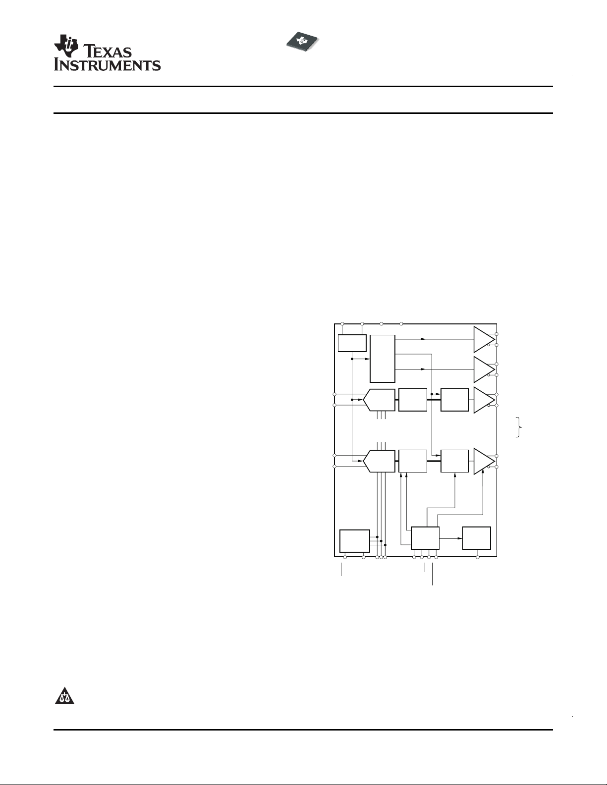
PRODUCTPREVIEW
10-Bit
ADC
PLL
Serializer
1xADCLK
6xADCLK
IN1
P
IN1
N
OUT1
P
OUT1
N
LCLK
P
LCLK
N
ADCLK
P
ADCLK
N
12xADCLK
10-Bit
ADC
Serializer
Digital
Digital
Reference
IN8
P
IN8
N
REF
T
INT/
EXT
REF
B
V
CM
OUT8
P
OUT8
N
I
SET
Registers
SDA
TA
C
S
RESET
SCLK
ADC
Control
PD
Clock
Buffer
(ADCLK)
CLK
P
(AVSS)
CLK
N
AVDD
(3.3V)
LVDD
(1.8V)
Power-
Down
TestPatterns
DriveCurrent
OutputFormat
DigitalGain
(0dBto12dB)
¼
¼
¼
¼
¼
¼
Channels
2to7
ADS5287
www.ti.com
SBAS428 – JANUARY 2008
10-Bit, Octal-Channel ADC Up to 65MSPS
1
FEATURES DESCRIPTION
23
• Speed and Resolution Grades:
– 10-bit, 65MSPS
• Power Dissipation:
– 46mW/Channel at 30MSPS
– 53mW/Channel at 40MSPS the ADS5287 is highly customizable for a diversity of
– 62mW/Channel at 50MSPS
– 74mW/Channel at 65MSPS
• 61.7dBFS SNR at 10MHz IF
• Analog Input Full-Scale Range: 2V
PP
• Low-Frequency Noise Suppression Mode
• 6dB Overload Recovery in One Clock
• External and Internal (Trimmed) Reference
• 3.3V Analog Supply, 1.8V Digital Supply
• Single-Ended or Differential Clock:
– Clock Duty Cycle Correction Circuit (DCC)
• Programmable Digital Gain: 0dB to 12dB
• Serialized DDR LVDS Output
• Programmable LVDS Current Drive, Internal
Termination
• Test Patterns for Enabling Output Capture
• Straight Offset Binary or Two's Complement
Output
• Package Options:
– 9mm × 9mm QFN-64
The ADS5287 is a high-performance, low-power,
octal channel analog-to-digital converter (ADC).
Available in a 9mm × 9mm QFN package, with
serialized low-voltage differential signaling (LVDS)
outputs and a wide variety of programmable features,
applications and offers an unprecedented level of
system integration. An application note, XAPP774
(available at www.xilinx.com ) describes how to
interface the serial LVDS outputs of TI's ADCs to
®
Xilinx
field-programmable gate arrays (FPGAs). The
ADS5287 is specified over the industrial temperature
range of – 40 ° C to +85 ° C.
APPLICATIONS
• Medical Imaging
• Wireless Base-Station Infrastructure
• Test and Measurement Instrumentation
1
Please be aware that an important notice concerning availability, standard warranty, and use in critical applications of
Texas Instruments semiconductor products and disclaimers thereto appears at the end of this data sheet.
2 Xilinx is a registered trademark of Xilinx, Inc.
3 All other trademarks are the property of their respective owners.
PRODUCT PREVIEW information concerns products in the
formative or design phase of development. Characteristic data and
other specifications are design goals. Texas Instruments reserves
the right to change or discontinue these products without notice.
Copyright © 2008, Texas Instruments Incorporated
www.ti.com
PRODUCTPREVIEW
ADS5287
SBAS428 – JANUARY 2008
This integrated circuit can be damaged by ESD. Texas Instruments recommends that all integrated circuits be handled with
appropriate precautions. Failure to observe proper handling and installation procedures can cause damage.
ESD damage can range from subtle performance degradation to complete device failure. Precision integrated circuits may be more
susceptible to damage because very small parametric changes could cause the device not to meet its published specifications.
ADS5281 12 50 8
ADS5282 12 65 8
ADS5287 10 65 8
ADS5270 12 40 8
ADS5271 12 50 8
ADS5272 12 65 8
ADS5273 12 70 8
ADS5242 12 65 4
RELATED PRODUCTS
MODEL RESOLUTION (BITS) SAMPLE RATE (MSPS) CHANNELS
PRODUCT PACKAGE-LEAD DESIGNATOR RANGE MARKING NUMBER MEDIA, QUANTITY
ADS5287 QFN-64 RGC – 40 ° C to +85 ° C AZ5287
(1) For the most current package and ordering information see the Package Option Addendum at the end of this document, or see the TI
web site at www.ti.com .
(2) These devices meet the following planned eco-friendly classification:
Green (RoHS and No Sb/Br): Texas Instruments defines Green to mean Pb-free (RoHS compatible) and free of bromine (Br)- and
antimony (Sb)-based flame retardants. Refer to the Quality and Lead-Free (Pb-Free) Data web site for more information. These devices
have a Cu NiPdAu lead/ball finish.
ABSOLUTE MAXIMUM RATINGS
Over operating free-air temperature range, unless otherwise noted.
Supply voltage range, AVDD – 0.3 to +3.9 V
Supply voltage range, LVDD – 0.3 to +2.2 V
Voltage between AVSS and LVSS – 0.3 to +0.3 V
External voltage applied to REF
External voltage applied to REF
Voltage applied to analog input pins – 0.3 to minimum [3.6, (AVDD + 0.3)] V
Voltage applied to digital input pins – 0.3 to minimum [3.9, (AVDD + 0.3)] V
Peak solder temperature +260 ° C
Junction temperature +125 ° C
Storage temperature range – 65 to +150 ° C
(1) Stresses above these ratings may cause permanent damage. Exposure to absolute maximum conditions for extended periods may
degrade device reliability. These are stress ratings only, and functional operation of the device at these or any other conditions beyond
those specified is not supported.
ORDERING INFORMATION
PACKAGE TEMPERATURE PACKAGE ORDERING TRANSPORT
(1)
pin – 0.3 to +3 V
T
pin – 0.3 to +2 V
B
SPECIFIED
(1) (2)
ADS5287IRGCT Tape and Reel, 250
ADS5287IRGCR Tape and Reel, 2000
ADS5287 UNIT
2 Submit Documentation Feedback Copyright © 2008, Texas Instruments Incorporated
Product Folder Link(s): ADS5287
www.ti.com
PRODUCTPREVIEW
ADS5287
SBAS428 – JANUARY 2008
RECOMMENDED OPERATING CONDITIONS
ADS5287
PARAMETER MIN TYP MAX UNIT
SUPPLIES, ANALOG INPUTS, AND REFERENCE VOLTAGES
AVDD Analog supply voltage 3.0 3.3 3.6 V
LVDD Digital supply voltage 1.7 1.8 1.9 V
Differential input voltage range 2 V
Input common-mode voltage VCM± 0.05 V
REF
REF
CLOCK INPUTS
DIGITAL OUTPUTS
C
LOAD
R
LOAD
T
A
External reference mode 2.5 V
T
External reference mode 0.5 V
B
ADCLK input sample rate 1/ t
Input clock amplitude differential (V
Sine wave, ac-coupled 3.0 V
LVPECL, ac-coupled 1.6 V
LVDS, ac-coupled 0.7 V
Input clock CMOS, single-ended (V
V
IL
V
IH
Input clock duty cycle 50 %
ADCLK
and ADCLK
P
LCLK
and LCLK
P
Maximum external capacitance from each pin to LVSS 5 pF
Differential load resistance between the LVDS output pairs 100 Ω
Operating free-air temperature – 40 +85 ° C
outputs (LVDS) 60 6x (sample rate) 300, 390 MHz
N
C
– V
CLKP
CLKP
outputs (LVDS) 10 1x (sample rate) 50, 65 MHz
N
) peak-to-peak
CLKN
)
10 50, 65 MSPS
0.6 V
2.2 V
PP
PP
PP
PP
INITIALIZATION REGISTERS
After the device has been powered up, the following registers must be written to (in the exact order listed) through the serial
interface as part of an initialization sequence.
Initialization register 1 03 0002
Initialization register 2 01 0010
Initialization register 3 C7 8001
Initialization register 4 DE 01C0
If the analog input is ac-coupled, register 5 must be be written to.
Initialization register 5 E2 00C0
Initializing these registers configures the device for the most optimum mode of operation.
ADDRESS (hex) DATA (hex)
ADDRESS (hex) DATA (hex)
Copyright © 2008, Texas Instruments Incorporated Submit Documentation Feedback 3
Product Folder Link(s): ADS5287
www.ti.com
PRODUCTPREVIEW
ADS5287
SBAS428 – JANUARY 2008
DIGITAL CHARACTERISTICS
DC specifications refer to the condition where the digital outputs are not switching, but are permanently at a valid logic level
'0' or '1'. At C
DIGITAL INPUTS
High-level input voltage 1.4 V
Low-level input voltage 0.3 V
High-level input current 33 µ A
Low-level input current – 33 µ A
Input capacitance 3 pF
LVDS OUTPUTS
High-level output voltage 1375 mV
Low-level output voltage 1025 mV
Output differential voltage, |V
V
output offset voltage Common-mode voltage of OUT
OS
Output capacitance 2 pF
(1) C
LOAD
(2) I
OUT
LOAD
PARAMETER TEST CONDITIONS MIN TYP MAX UNIT
is the effective external single-ended load capacitance between each output pin and ground.
refers to the LVDS buffer current setting; R
(1)
= 5pF
, I
= 3.5mA
OUT
(2)
, R
= 100 Ω
LOAD
(2)
, and no internal termination, unless otherwise noted.
ADS5287
| 350 mV
OD
and OUT
P
N
1200 mV
Output capacitance inside the device,
from either output to ground
is the differential load resistance between the LVDS output pair.
LOAD
4 Submit Documentation Feedback Copyright © 2008, Texas Instruments Incorporated
Product Folder Link(s): ADS5287
www.ti.com
PRODUCTPREVIEW
ELECTRICAL CHARACTERISTICS
Typical values at +25 ° C. Minimum and maximum values are measured across the specified temperature range of T
– 40 ° C to T
differential analog input, internal reference mode, I
otherwise noted.Typical values at +25 ° C.
INTERNAL REFERENCE VOLTAGES
V
REFB
V
REFT
V
CM
EXTERNAL REFERENCE VOLTAGES
V
REFB
V
REFT
ANALOG INPUT
DC ACCURACY
DC PSRR DC power-supply rejection ratio
POWER-DOWN MODES
DYNAMIC PERFORMANCE
DC ACCURACY
DNL Differential nonlinearity – 0.5 ± 0.1 +0.5 LSB
INL Integral nonlinearity – 1 ± 0.1 +1 LSB
= +85 ° C, AVDD = 3.3V, LVDD = 1.8V, clock frequency = 10MSPS to 65MSPS, 50% clock duty cycle, – 1dBFS
MAX
PARAMETER TEST CONDITIONS MIN TYP MAX UNIT
Reference bottom 0.5 V
Reference top 2.5 V
V
– V
REFT
REFB
Common-mode voltage (internal) 1.425 1.5 1.575 V
VCMoutput current ± 2 mA
Reference bottom 0.4 0.5 0.6 V
Reference top 2.4 2.5 2.6 V
V
– V
REFT
REFB
Differential input voltage range 2.0 V
Differential input capacitance 3 pF
Analog input bandwidth 520 MHz
Analog input common-mode range DC-coupled input VCM± 0.05 V
Analog input common-mode current 2.5
Voltage overload recovery time 1 Clock cycle
Voltage overload recovery repeatability first data within full-scale range in a 6dB 1 LSB
Offset error – 1.25 ± 0.2 +1.25 %FS
Offset error temperature coefficient
Channel gain error Excludes error in internal reference – 0.8 %FS
Channel gain error temperature Excludes temperature coefficient of
coefficient internal reference
Internal reference error temperature
coefficient
Power in complete power-down mode 45 mW
Power in partial power-down mode Clock at 65MSPS 135 mW
Power with no clock 88 mW
Crosstalk channels, measurement taken on channel – 90 dBc
Two-tone, third-order intermodulation f1= 9.5MHz at – 7dBFs
distortion f2= 10.2MHz at – 7dBFs
No missing codes Assured
(2)
ADS5287
SBAS428 – JANUARY 2008
=
MIN
resistor = 56.2k Ω , and LVDS buffer current setting = 3.5mA, unless
SET
ADS5287
1.95 2.0 2.05 V
1.9 2.0 2.1 V
PP
Per input pin per MSPS of sampling µ A/MHz
Recovery from 6dB overload to within 1%
Standard deviation seen on a periodic
(1)
(3)
5MHz full-scale signal applied to seven
speed per pin
accuracy
overloaded sine wave
± 5 ppm/ ° C
± 10 ppm/ ° C
± 15 ppm/ ° C
1.5 mV/V
with no input signal
– 92 dBFS
(1) The offset temperature coefficient in ppm/ ° C is defined as (O
at the two extreme temperatures, T1and T2.
1
– O2) × 10
(2) The internal reference temperature coefficient is defined as (REF
reference voltages (REF
(3) DC PSRR is defined as the ratio of the change in the ADC output (expressed in mV) to the change in supply voltage (in volts).
Copyright © 2008, Texas Instruments Incorporated Submit Documentation Feedback 5
– REF
T
) at the two extreme temperatures, T1and T2.
B
6
/(T
– T2)/1024, where O1and O2are the offset codes in LSB
1
– REF
1
6
) × 10
/(T
2
– T2)/2, where REF
1
and REF
1
are the internal
2
Product Folder Link(s): ADS5287
www.ti.com
PRODUCTPREVIEW
ADS5287
SBAS428 – JANUARY 2008
ELECTRICAL CHARACTERISTICS (continued)
Typical values at +25 ° C. Minimum and maximum values are measured across the specified temperature range of T
– 40 ° C to T
differential analog input, internal reference mode, I
otherwise noted.Typical values at +25 ° C.
POWER SUPPLY — INTERNAL REFERENCE MODE
IAVDD Analog supply current 139 TBD mA
ILVDD Digital current Zero input to all channels 87 TBD mA
POWER SUPPLY — EXTERNAL REFERENCE MODE
IAVDD Analog supply current 132 mA
ILVDD Digital current Zero input to all channels 87 mA
EXTERNAL REFERENCE LOADING
DYNAMIC CHARACTERISTICS
SFDR Spurious-free dynamic range
HD2 Magnitude of second harmonic
HD3 Magnitude of third harmonic
THD Total harmonic distortion
SNR Signal-to-noise ratio
SINAD Signal-to-noise and distortion
= +85 ° C, AVDD = 3.3V, LVDD = 1.8V, clock frequency = 10MSPS to 65MSPS, 50% clock duty cycle, – 1dBFS
MAX
PARAMETER TEST CONDITIONS MIN TYP MAX UNIT
Total power 615 TBD mW
Incremental power saving 61 mW
Total power 592 mW
Incremental power saving 59 mW
Switching current external reference voltages; sourcing for 3.5 mA
resistor = 56.2k Ω , and LVDS buffer current setting = 3.5mA, unless
SET
ADS5287
Obtained on powering down one channel
Obtained on powering down one channel
Current drawn by the eight ADCs from the
fIN= 5MHz, single-ended clock 73 85 dBc
fIN= 30MHz, differential clock 80 dBc
fIN= 5MHz, single-ended clock 73 85 dBc
fIN= 30MHz, differential clock 82 dBc
fIN= 5MHz, single-ended clock 73 85 dBc
fIN= 30MHz, differential clock 80 dBc
fIN= 5MHz, single-ended clock 70 80 dBc
fIN= 30MHz, differential clock 78 dBc
fIN= 5MHz, single-ended clock 60.5 61.7 dBc
fIN= 30MHz, differential clock 61.7 dBc
fIN= 5MHz, single-ended clock 60.4 61.6 dBc
fIN= 30MHz, differential clock 61.6 dBc
at a time
at a time
REF
, sinking for REF
T
.
B
=
MIN
6 Submit Documentation Feedback Copyright © 2008, Texas Instruments Incorporated
Product Folder Link(s): ADS5287
www.ti.com
PRODUCTPREVIEW
48
47
46
45
44
43
42
41
40
39
38
37
36
35
34
33
IN8
N
IN8
P
AVSS
IN7
N
IN7
P
AVSS
IN6
N
IN6
P
AVSS
IN5
N
IN5
P
AVSS
LVSS
LVDD
OUT8
N
OUT8
P
1
2
3
4
5
6
7
8
9
10
11
12
13
14
15
16
IN1
P
IN1
N
AVSS
IN2
P
IN2
N
AVSS
IN3
P
IN3
N
AVSS
IN4
P
IN4
N
LVSS
PD
LVSS
OUT1
P
OUT1
N
RESET
SCLK
SDATA
CS
AVDD
CLKNCLKPAVDD
INT/EXT
REFTREFBV
C
M
TP
I
SET
AVDD
AVDD
OUT2
P
OUT2
N
OUT3
P
OUT3
N
OUT4
P
OUT4
N
ADCLK
P
ADCLK
N
LCLK
P
LCLK
N
OUT5
P
OUT5
N
OUT6
P
OUT6
N
OUT7
P
OUT7
N
64
63 62 61 60 59 58
57 56 55 54
17 18 19 20 21 22 23 24 25 26 27
53 52 51 50 49
28 29 30 31 32
ADS5287
ADS5287
SBAS428 – JANUARY 2008
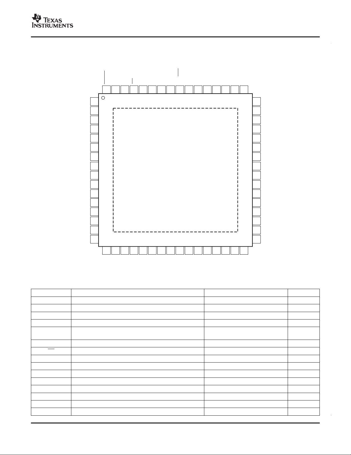
PIN CONFIGURATION
QFN-64 PowerPAD
TOP VIEW
PIN NAME DESCRIPTION PIN NUMBER # OF PINS
ADCLK
N
ADCLK
P
AVDD Analog power supply, 3.3V 49, 50, 57, 60 4
AVSS Analog ground 3, 6, 9, 37, 40, 43, 46 7
CLK
N
CLK
P
CS Serial enable chip select — active low digital input 61 1
IN1
N
IN1
P
IN2
N
IN2
P
IN3
N
IN3
P
IN4
N
IN4
P
Copyright © 2008, Texas Instruments Incorporated Submit Documentation Feedback 7
LVDS frame clock (1X) — negative output 24 1
LVDS frame clock (1X) — positive output 23 1
Negative differential clock input
Tie CLK
Positive differential clock input 58 1
Negative differential input signal, channel 1 2 1
Positive differential input signal, channel 1 1 1
Negative differential input signal, channel 2 5 1
Positive differential input signal, channel 2 4 1
Negative differential input signal, channel 3 8 1
Positive differential input signal, channel 3 7 1
Negative differential input signal, channel 4 11 1
Positive differential input signal, channel 4 10 1
to 0V for a single-ended clock
N
Table 1. PIN DESCRIPTIONS: QFN-64
Product Folder Link(s): ADS5287
59 1
www.ti.com
PRODUCTPREVIEW
ADS5287
SBAS428 – JANUARY 2008
PIN NAME DESCRIPTION PIN NUMBER # OF PINS
IN5
N
IN5
P
IN6
N
IN6
P
IN7
N
IN7
P
IN8
N
IN8
P
INT/ EXT Internal/external reference mode select input 56 1
I
SET
LCLK
N
LCLK
P
LVDD Digital and I/O power supply, 1.8V 35 1
LVSS Digital ground 12, 14, 36 3
OUT1
N
OUT1
P
OUT2
N
OUT2
P
OUT3
N
OUT3
P
OUT4
N
OUT4
P
OUT5
N
OUT5
P
OUT6
N
OUT6
P
OUT7
N
OUT7
P
OUT8
N
OUT8
P
PD Power-down input 13 1
REF
B
REF
T
RESET Active low RESET input 64 1
SCLK Serial clock input 63 1
SDATA Serial data input 62 1
TP Test pin, do not use 52 1
V
CM
Negative differential input signal, channel 5 39 1
Positive differential input signal, channel 5 38 1
Negative differential input signal, channel 6 42 1
Positive differential input signal, channel 6 41 1
Negative differential input signal, channel 7 45 1
Positive differential input signal, channel 7 44 1
Negative differential input signal, channel 8 48 1
Positive differential input signal, channel 8 47 1
Bias pin — 56.2k Ω to ground 51 1
LVDS bit clock (6X) — negative output 26 1
LVDS bit clock (6X) — positive output 25 1
LVDS channel 1 — negative output 16 1
LVDS channel 1 — positive output 15 1
LVDS channel 2 — negative output 18 1
LVDS channel 2 — positive output 17 1
LVDS channel 3 — negative output 20 1
LVDS channel 3 — positive output 19 1
LVDS channel 4 — negative output 22 1
LVDS channel 4 — positive output 21 1
LVDS channel 5 — negative output 28 1
LVDS channel 5 — positive output 27 1
LVDS channel 6 — negative output 30 1
LVDS channel 6 — positive output 29 1
LVDS channel 7 — negative output 32 1
LVDS channel 7 — positive output 31 1
LVDS channel 8 — negative output 34 1
LVDS channel 8 — positive output 33 1
Negative reference input/output 54 1
Positive reference input/output 55 1
Common-mode output pin, 1.5V output 53 1
Table 1. PIN DESCRIPTIONS: QFN-64 (continued)
8 Submit Documentation Feedback Copyright © 2008, Texas Instruments Incorporated
Product Folder Link(s): ADS5287
www.ti.com
PRODUCTPREVIEW
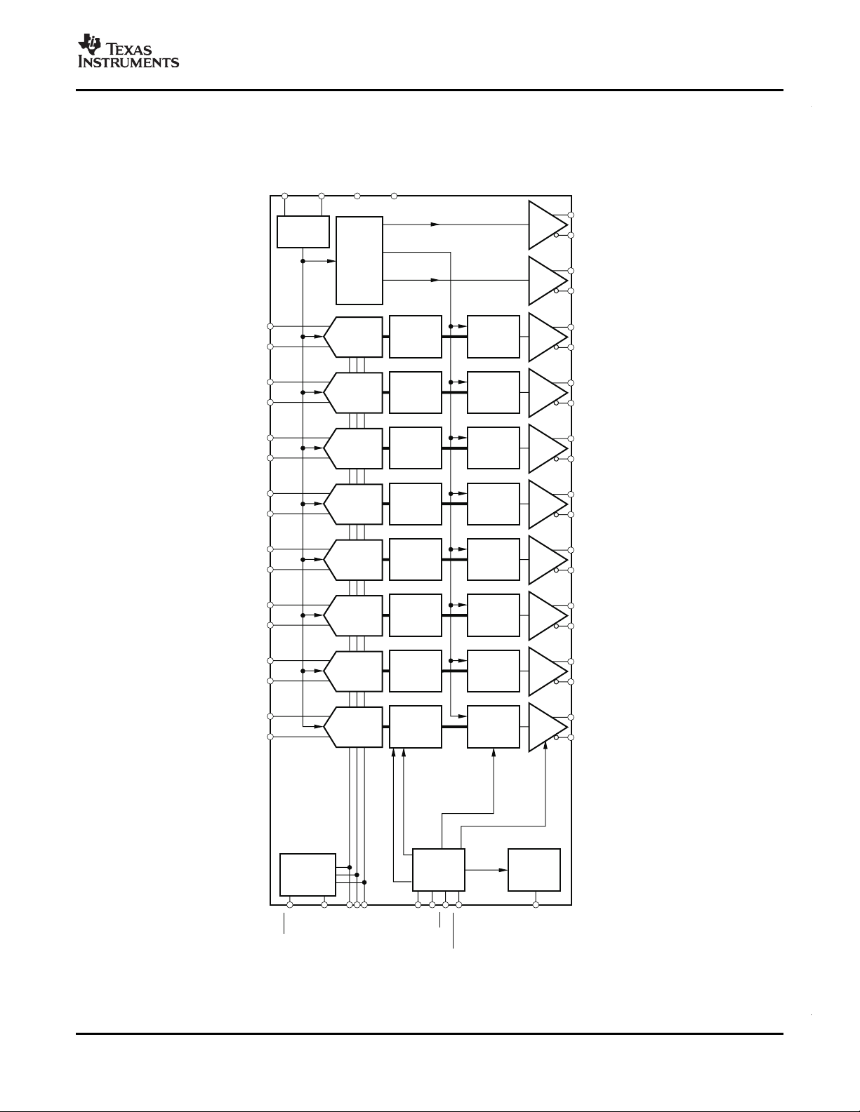
10-Bit
ADC
PLL
Serializer
1xADCLK
6xADCLK
IN1
P
IN1
N
OUT1
P
OUT1
N
10-Bit
ADC
Serializer
IN2
P
IN2
N
OUT2
P
OUT2
N
10-Bit
ADC
Serializer
IN3
P
IN3
N
OUT3
P
OUT3
N
LCLK
P
LCLK
N
ADCLK
P
ADCLK
N
12xADCLK
10-Bit
ADC
Serializer
IN4
P
IN4
N
OUT4
P
OUT4
N
10-Bit
ADC
Serializer
IN5
P
IN5
N
OUT5
P
OUT5
N
10-Bit
ADC
Serializer
IN6
P
IN6
N
OUT6
P
OUT6
N
10-Bit
ADC
Serializer
IN7
P
IN7
N
OUT7
P
OUT7
N
10-Bit
ADC
Serializer
Digital
Digital
Digital
Digital
Digital
Digital
Digital
Digital
Reference
IN8
P
IN8
N
REF
T
INT/
EXT
REF
B
V
CM
OUT8
P
OUT8
N
I
SET
Registers
SDATA
CS
RESET
SCLK
ADC
Control
PD
Clock
Buffer
(ADCLK)
CLK
P
(AVSS)
CLK
N
AVDD
(3.3V)
L
VDD
(1.8V)
Power-
Down
T
estP
atterns
DriveCurrent
OutputFormat
DigitalGain
(0dBto12dB)
ADS5287
SBAS428 – JANUARY 2008
FUNCTIONAL BLOCK DIAGRAM
Copyright © 2008, Texas Instruments Incorporated Submit Documentation Feedback 9
Product Folder Link(s): ADS5287
www.ti.com
PRODUCTPREVIEW
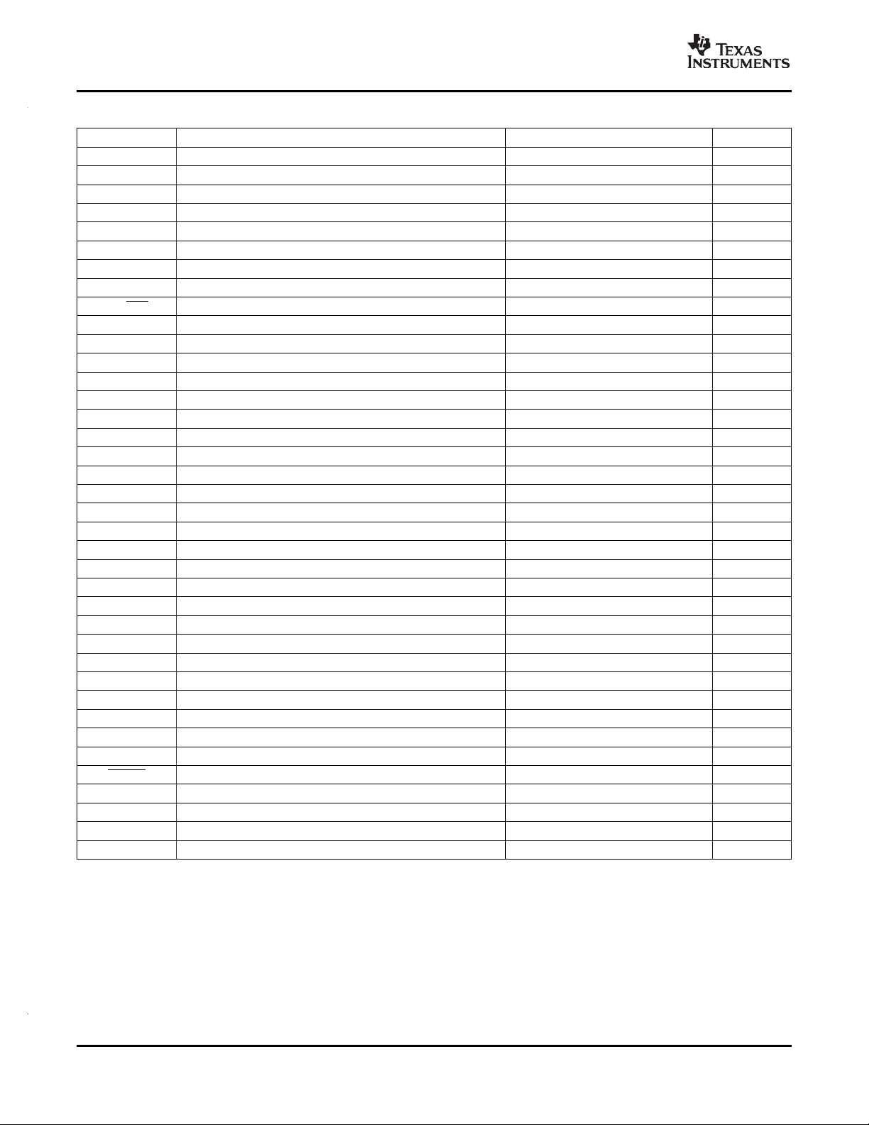
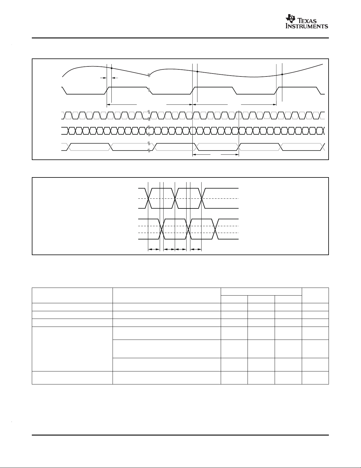
0 0 D0 D1 D2 D3 D4 D5 D6 D7 D8 D9 0 0 D0 D1 D2 D3 D4 D5 D6 D7 D8 D90 0 D0 D1 D2 D3 D4 D5 D6 D7 D8 D9
Sample n
Sample n+12
t
PROP
t (A)
D
12clockslatency
AnalogInput
ClockInput
6XADCLK
LCLK
N
LCLK
P
1XADCLK
ADCLK
N
ADCLK
P
SERIAL DATA
OUT
P
OUT
N
t
SAMPLE
Sample n+13
t
H1tSU1tH2tSU2
LCLK
N
LCLK
P
OUT
N
OUT
P
ADS5287
SBAS428 – JANUARY 2008
LVDS TIMING DIAGRAM
DEFINITION OF SETUP AND HOLD TIMES
tSU= min(t
tH= min(t
TIMING CHARACTERISTICS
t
A
t
J
t
WAKE
(1) Timing parameters are ensured by design and characterization; not production tested.
, t
, tH2)
)
SU2
SU1
H1
PARAMETER TEST CONDITIONS MIN TYP MAX UNIT
Aperture delay 1.5 4.5 ns
Aperture delay variation Channel-to-channel within the same device (3 σ ) ± 20 ps
Aperture jitter 400 fs
Wake-up time POWER-DOWN mode (with clock continuing to 2 µ s
Data latency 12
(1)
Time to valid data after coming out of
COMPLETE POWER-DOWN mode
Time to valid data after coming out of PARTIAL
run during power-down)
Time to valid data after stopping and restarting
the input clock
ADS5287
50 µ s
40 µ s
Clock
cycles
10 Submit Documentation Feedback Copyright © 2008, Texas Instruments Incorporated
Product Folder Link(s): ADS5287
 Loading...