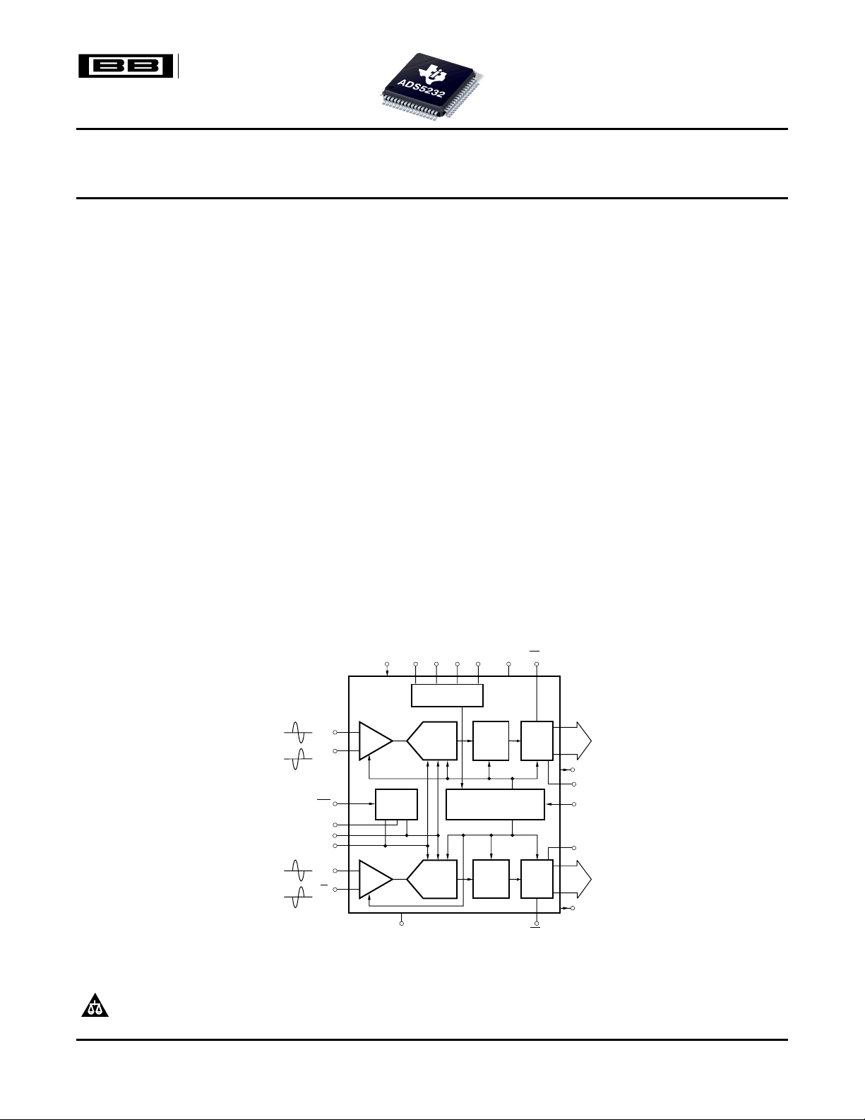
12-Bit
Pipelined
ADC
Error
Correction
Logic
Timing/Duty Cycle
Adjust (PLL)
Internal
Reference
3-State
Output
S/H
D11A
·
·
·
D0A
12-Bit
Pipelined
ADC
Error
Correction
Logic
3-State
Output
S/H
D11B
·
·
·
D0B
AV
DD
OE
A
V
DRV
SDATA SEN SCLK SEL
OVR
A
OVR
B
IN
A
CM
IN
A
INT/EXT
CLK
DV
A
DV
B
REFT
REFB
IN
B
V
IN
OE
B
STPD
IN
B
ADS5232
V
IN
Serial
Interface
DISABLE_PLL
Dual, 12-Bit, 65MSPS, +3.3V
Analog-to-Digital Converter
FEATURES DESCRIPTION
• Single +3.3V Supply
• High SNR: 70.7dBFS at fIN= 5MHz
• Total Power Dissipation:
Internal Reference: 371mW
External Reference: 335mW
• Internal or External Reference
• Low DNL: ±0.3LSB
• Flexible Input Range: 1.5V
• TQFP-64 Package
APPLICATIONS
• Communications IF Processing
• Communications Base Stations
• Test Equipment
• Medical Imaging
• Video Digitizing
• CCD Digitizing
to 2V
PP
ADS5232
SBAS294A – JUNE 2004 – REVISED MARCH 2006
The ADS5232 is a dual, high-speed, high dynamic
range, 12-bit pipelined analog-to-digital converter
(ADC). This converter includes a high-bandwidth
sample-and-hold amplifier that gives excellent
spurious performance up to and beyond the Nyquist
rate. The differential nature of the sample-and-hold
amplifier and ADC circuitry minimizes even-order
harmonics and gives excellent common-mode noise
PP
immunity.
The ADS5232 provides for setting the full-scale range
of the converter without any external reference
circuitry. The internal reference can be disabled,
allowing low-drive, external references to be used for
improved tracking in multichannel systems.
The ADS5232 provides an over-range indicator flag
to indicate an input signal that exceeds the full-scale
input range of the converter. This flag can be used to
reduce the gain of front-end gain control circuitry.
There is also an output enable pin to allow for
multiplexing and testing on a PC board.
The ADS5232 employs digital error correction
techniques to provide excellent differential linearity for
demanding imaging applications. The ADS5232 is
available in a TQFP-64 package.
All trademarks are the property of their respective owners.
PRODUCTION DATA information is current as of publication date.
Products conform to specifications per the terms of the Texas
Instruments standard warranty. Production processing does not
necessarily include testing of all parameters.
Please be aware that an important notice concerning availability, standard warranty, and use in critical applications of Texas
Instruments semiconductor products and disclaimers thereto appears at the end of this data sheet.
Copyright © 2004–2006, Texas Instruments Incorporated
www.ti.com
ADS5232
SBAS294A – JUNE 2004 – REVISED MARCH 2006
This integrated circuit can be damaged by ESD. Texas Instruments recommends that all integrated circuits be handled with
appropriate precautions. Failure to observe proper handling and installation procedures can cause damage.
ESD damage can range from subtle performance degradation to complete device failure. Precision integrated circuits may be more
susceptible to damage because very small parametric changes could cause the device not to meet its published specifications.
ORDERING INFORMATION
PRODUCT PACKAGE-LEAD DESIGNATOR RANGE MARKING NUMBER MEDIA, QUANTITY
ADS5232 TQFP-64 PAG –40°C to +85°C ADS5232IPAG
(1) For the most current package and ordering information see the Package Option Addendum at the end of this document, or see the TI
website at www.ti.com .
ABSOLUTE MAXIMUM RATINGS
PACKAGE TEMPERATURE PACKAGE ORDERING TRANSPORT
(1)
SPECIFIED
(1)
ADS5232IPAG Tray, 160
ADS5232IPAGT Tape and Reel, 250
over operating free-air temperature range (unless otherwise noted)
Supply Voltage Range, AVDD –0.3V to +3.8V
Supply Voltage Range, VDRV –0.3V to +3.8V
Voltage Between AVDD and VDRV –0.3V to +0.3V
Voltage Applied to External REF Pins –0.3V to +2.4V
Analog Input Pins
Case Temperature +100°C
Operating Free-Air Temperature Range, T
Lead Temperature +260°C
Junction Temperature +105°C
Storage Temperature –65°C +150°C
(1) Stresses above those listed under Absolute Maximum Ratings may cause permanent damage to the device. Exposure to absolute
maximum conditions for extended periods may affect device reliability.
(2) The DC voltage applied on the input pins should not go below –0.3V. Also, the DC voltage should be limited to the lower of either 3.3V
or (AVDD + 0.3V). If the input can go higher than +3.3V, then a resistor greater than or equal to 25 Ω should be added in series with
each of the input pins. Also, the duty cycle of the overshoot beyond +3.3V should be limited. The overshoot duty cycle can be defined
either as a percentage of the time of overshoot over a clock period, or over the entire device lifetime. For a peak voltage between +3.3V
and +3.5V, a duty cycle up to 10% is acceptable. For a peak voltage between +3.5V and +3.7V, the overshoot duty cycle should not
exceed 1%. Any overshoot beyond +3.7V should be restricted to less than 0.1% duty cycle, and never exceed +3.9V.
(2)
A
–0.3V to min [3.3V, (AVDD + 0.3V)]
–40°C to +85°C
2
Submit Documentation Feedback

www.ti.com
SBAS294A – JUNE 2004 – REVISED MARCH 2006
RECOMMENDED OPERATING CONDITIONS
ADS5232
MIN TYP MAX UNITS
SUPPLIES AND REFERENCES
Analog Supply Voltage, AVDD 3.0 3.3 3.6 V
Output Driver Supply Voltage, VDRV 3.0 3.3 3.6 V
REF
— External Reference Mode 1.875 2.0 2.05 V
T
REF
— External Reference Mode 0.95 1.0 1.125 V
B
REFCM = (REF
Reference = (REF
Analog Input Common-Mode Range
+ REF
T
)/2 – External Reference Mode
B
– REF
T
) – External Reference Mode 0.75 1.0 1.1 V
B
(1)
CLOCK INPUT AND OUTPUTS
ADCLK Input Sample Rate
PLL Enabled (default) 20 65 MSPS
PLL Disabled 2 30
ADCLK Duty Cycle
PLL Enabled (default) 45 55 MSPS
Low-Level Voltage Clock Input 0.6 V
High-Level Voltage Clock Input 2.2 V
Operating Free-Air Temperature, T
A
Thermal Characteristics:
θ
JA
θ
JC
(1) These voltages need to be set to 1.5V ± 50mV if they are derived independent of VCM.
(2) When the PLL is disabled, the clock duty cycle needs to be controlled well, especially at higher speeds. A 45%–55% duty cycle variation
is acceptable up to a frequency of 30MSPS. If the device needs to be operated in the PLL disabled mode beyond 30MSPS, then the
duty cycle needs to be maintained within 48%–52% duty cycle.
(1)
V
± 50mV V
CM
V
± 50mV V
CM
(2)
–40 +85 °C
42.8 °C/W
18.7 °C/W
ADS5232
MSPS
Submit Documentation Feedback
3

www.ti.com
ADS5232
SBAS294A – JUNE 2004 – REVISED MARCH 2006
ELECTRICAL CHARACTERISTICS
T
= –40°C and T
MIN
AVDD = 3.3V, VDRV = 3.3V, transformer-coupled inputs, –1dBFS, I
otherwise noted.
DC ACCURACY
No Missing Codes Tested
DNL Differential Nonlinearity fIN= 5MHz –0.9 ±0.3 +0.9 LSB
INL Integral Nonlinearity fIN= 5MHz –2.5 ±0.4 +2.5 LSB
Offset Error
Offset Temperature Coefficient
Fixed Attenuation in Channel
Fixed Attenuation Matching Across Channels 0.01 0.2 dB
Gain Error/Reference Error
Gain Error Temperature Coefficient ±40 ppm/°C
POWER REQUIREMENTS
Internal Reference
Power Dissipation
Total Power Dissipation 371 439 mW
External Reference
Power Dissipation Analog Only (AVDD) 224 mW
Total Power Dissipation 335 mW
VREF
T
VREF
B
Total Power-Down 88 mW
REFERENCE VOLTAGES
VREF
Reference Top (internal) 1.9 2.0 2.1 V
T
VREF
VREF
(1) Offset error is the deviation of the average code from mid-code with –1dBFS sinusoid from ideal mid-code (2048). Offset error is
(2) If the offset at temperatures T1and T2are O1and O2, respectively (where O1and O2are measured in LSBs), the offset temperature
(3) Fixed attenuation in the channel arises because of a fixed attenuation in the sample-and-hold amplifier. When the differential voltage at
(4) The reference voltages are trimmed at production so that (VREF
(5) Supply current can be calculated from dividing the power dissipation by the supply voltage of 3.3V.
(6) The V
(7) Average current drawn from the reference pins in the external reference mode.
Reference Bottom (internal) 0.9 1.0 1.1 V
B
V
Common-Mode Voltage 1.4 1.5 1.6 V
CM
V
Output Current
CM
VREF
Reference Top (external) 1.875 V
T
Reference Bottom (external) 1.125 V
B
External Reference Common-Mode V
External Reference Input Current
expressed in terms of % of full-scale.
coefficient in ppm/°C is calculated as (O
the analog input pins is changed from –V
(4096LSB) by the extent of this fixed attenuation. NOTE: V
does not include fixed attenuation.
output current specified is the drive of the V
CM
= +85°C. Typical values are at TA= +25°C, clock frequency = 65MSPS, 50% clock duty cycle,
MAX
= 56.2k Ω , and internal voltage reference, unless
SET
ADS5232
PARAMETER TEST CONDITIONS MIN TYP MAX UNITS
(1)
(2)
(3)
(4)
(5)
(5)
Analog Only (AVDD) 260 297 mW
–0.75 ±0.2 +0.75 %FS
±6 ppm/°C
1 %FS
–3.5 ±1.0 +3.5 % FS
Output Driver (VDRV) 111 142 mW
Output Driver (VDRV) 111 mW
1.875 2 2.05 mW
0.95 1 1.125 mW
(6)
(7)
– O2)/(T
1
to +V
REF
±50mV Change in Voltage ±2 mA
± 50mV V
CM
1.0 mA
– T2) × 1E6/4096.
1
, the swing of the output code is expected to deviate from the full-scale code
REF
CM
REF
buffer if loaded externally.
is defined as (REF
– VREF
T
– REF
T
) is within ± 35mV of the ideal value of 1V. This specification
B
).
B
4
Submit Documentation Feedback
www.ti.com
SBAS294A – JUNE 2004 – REVISED MARCH 2006
ELECTRICAL CHARACTERISTICS (continued)
T
= –40°C and T
MIN
AVDD = 3.3V, VDRV = 3.3V, transformer-coupled inputs, –1dBFS, I
otherwise noted.
ANALOG INPUT
Differential Input Capacitance 3 pF
Analog Input Common-Mode Range V
Differential Input Voltage Range Internal Reference 2.02 V
Voltage Overload Recovery Time
Input Bandwidth 300 MHz
DIGITAL DATA INPUTS
Logic Family +3V CMOS Compatible
V
High-Level Input Voltage VIN= 3.3V 2.2 V
IH
V
Low-Level Input Voltage VIN= 3.3V 0.6 V
IL
C
Input Capacitance 3 pF
IN
DIGITAL OUTPUTS
Data Format Straight Offset Binary
Logic Family CMOS
Logic Coding Straight Offset Binary or BTC
Low Output Voltage (I
High Output Voltage (I
3-State Enable Time 2 Clocks
3-State Disable Time 2 Clocks
Output Capacitance 3 pF
SERIAL INTERFACE
SCLK Serial Clock Input Frequency 20 MHz
CONVERSION CHARACTERISTICS
Sample Rate 20 65 MSPS
Data Latency 6 CLK Cycles
(8) A differential ON/OFF pulse is applied to the ADC input. The differential amplitude of the pulse in its ON (high) state is twice the
full-scale range of the ADC, while the differential amplitude of the pulse in its OFF (low) state is zero. The overload recovery time of the
ADC is measured as the time required by the ADC output code to settle within 1% of full-scale, as measured from its mid-code value
when the pulse is switched from ON (high) to OFF (low).
(9) Option for Binary Two’s Complement Output.
= +85°C. Typical values are at TA= +25°C, clock frequency = 65MSPS, 50% clock duty cycle,
MAX
= 56.2k Ω , and internal voltage reference, unless
SET
ADS5232
PARAMETER TEST CONDITIONS MIN TYP MAX UNITS
± 0.05 V
CM
External Reference 2.02 × (VREF
(8)
– VREF
T
B
3 CLK Cycles
–3dBFS Input, 25 Ω Series
Resistance
(9)
= 50µA) +0.4 V
OL
= 50µA) +2.4 V
OH
) V
ADS5232
PP
PP
Submit Documentation Feedback
5
www.ti.com
ADS5232
SBAS294A – JUNE 2004 – REVISED MARCH 2006
AC CHARACTERISTICS
T
= –40°C and T
MIN
cycle, AVDD = 3.3V, VDRV = 3.3V, –1dBFS, I
PARAMETER CONDITIONS MIN TYP MAX UNITS
DYNAMIC CHARACTERISTICS
SFDR Spurious-Free Dynamic Range fIN= 32.5MHz 85 dBc
HD
2nd-Order Harmonic Distortion fIN= 32.5MHz 87 dBc
2
HD
3rd-Order Harmonic Distortion fIN= 32.5MHz 85 dBc
3
SNR Signal-to-Noise Ratio fIN= 32.5MHz 69.5 dBFS
SINAD Signal-to-Noise and Distortion fIN= 32.5MHz 69 dBFS
Crosstalk –85 dBc
Two-Tone, Third-Order
IMD3 90.9 dBFS
Intermodulation Distortion
= +85°C. Typical values are at TA= +25°C, clock frequency = maximum specified, 50% clock duty
MAX
= 56.2k Ω , and internal voltage reference, unless otherwise noted.
SET
fIN= 5MHz 75 86 dBc
fIN= 70MHz 83 dBc
fIN= 5MHz 82 92 dBc
fIN= 70MHz 85 dBc
fIN= 5MHz 75 86 dBc
fIN= 70MHz 83 dBc
fIN= 5MHz 68 70.7 dBFS
fIN= 70MHz 67.5 dBFS
fIN= 5MHz 67.5 70.3 dBFS
fIN= 70MHz 67 dBFS
5MHz Full-Scale Signal Applied to 1 Channel;
Measurement Taken on the Channel with No Input Signal
f1= 4MHz at –7dBFS
f2= 5MHz at –7dBFS
ADS5242
6
Submit Documentation Feedback
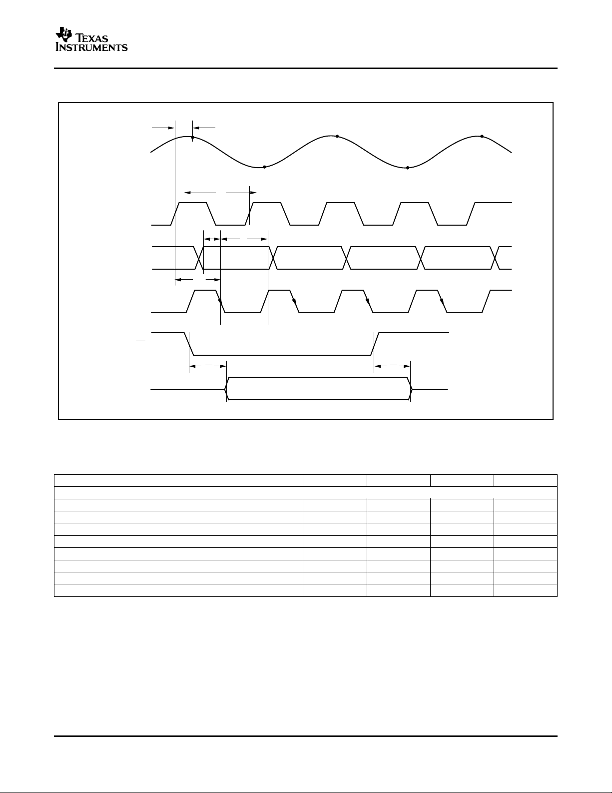
www.ti.com
Analog
Input
CLK
DATA[D11:D0]
DV
OE
DATA
D11:D0
t
OE
t
OE
t
DV
t
1
t
2
t
C
t
A
N + 1
N + 2 N+4
N + 3
N
ADS5232
SBAS294A – JUNE 2004 – REVISED MARCH 2006
TIMING DIAGRAM
TIMING CHARACTERISTICS
(1)
Typical values at TA= +25°C, AVDD = VDRV = 3.3V, sampling rate and PLL state are as indicated, input clock at 50% duty
cycle, and total capacitive loading = 10pF, unless otherwise noted.
PARAMETER MIN TYP MAX UNITS
tAAperture Delay 2.1 ns
Aperture Jitter 1.0 ps
tDR, tDFData Rise/Fall Time
t1Data Setup Time
t2Data Hold Time
tDData Latency 6 Clocks
Data Valid (DV) Duty Cycle 30 40 55 %
tDVInput Clock Rising to DV Fall Edge 10 11.5 14 ns
(1) Specifications assured by design and characterization; not production tested.
(2) Measured from data becoming valid (at a high level = 2.0V and a low level = 0.8V) to the 50% point of the falling edge of DV.
(3) Measured from the 50% point of the falling edge of DV to the data becoming invalid.
(4) Measured between 20% to 80% of logic levels.
(2)
(3)
(4)
65MSPS With PLL ON
2 3.2 ns
6.3 8.5 ns
0.5 2 3 ns
Submit Documentation Feedback
7
www.ti.com
ADS5232
SBAS294A – JUNE 2004 – REVISED MARCH 2006
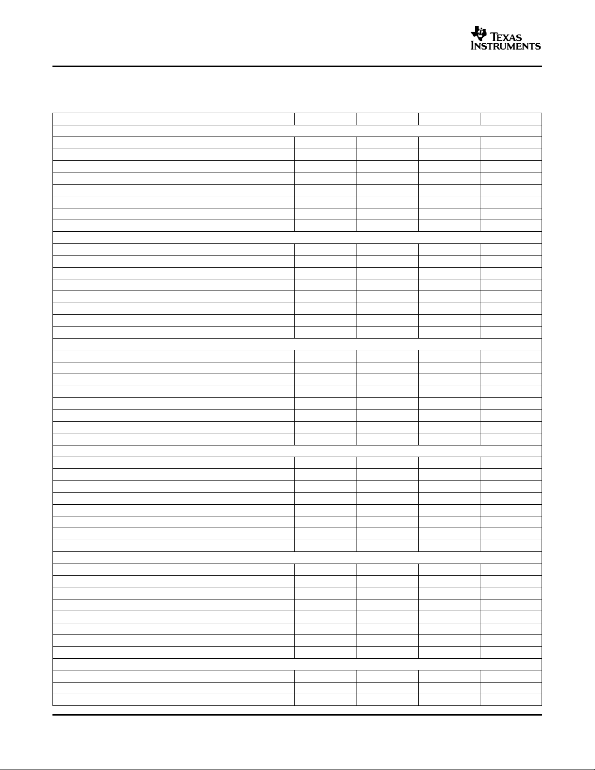
TIMING CHARACTERISTICS (continued)
Typical values at TA= +25°C, AVDD = VDRV = 3.3V, sampling rate and PLL state are as indicated, input clock at 50% duty
cycle, and total capacitive loading = 10pF, unless otherwise noted.
PARAMETER MIN TYP MAX UNITS
50MSPS With PLL ON
tAAperture Delay 2.1 ns
Aperture Jitter 1.0 ps
t1Data Setup Time 3.2 4.5 ns
t2Data Hold Time 10 11 ns
tDData Latency 6 Clocks
tDR, tDFData Rise/Fall Time 0.5 2 3 ns
Data Valid (DV) Duty Cycle 30 40 55 %
tDVInput Clock Rising to DV Fall Edge 11.5 13.5 15.5 ns
40MSPS With PLL ON
tAAperture Delay 2.1 ns
Aperture Jitter 1.0 ps
t1Data Setup Time 3.7 5.5 ns
t2Data Hold Time 11.5 13.5 ns
tDData Latency 6 Clocks
tDR, tDFData Rise/Fall Time 0.5 2 3 ns
Data Valid (DV) Duty Cycle 30 40 55 %
tDVInput Clock Rising to DV Fall Edge 13.5 16 18.5 ns
30MSPS With PLL OFF
tAAperture Delay 2.1 ns
Aperture Jitter 1.0 ps
t1Data Setup Time 8 10 ns
t2Data Hold Time 14 19 ns
tDData Latency 6 Clocks
tDR, tDFData Rise/Fall Time 0.5 2 3.5 ns
Data Valid (DV) Duty Cycle 30 45 55 %
tDVInput Clock Rising to DV Fall Edge 16 19 21 ns
20MSPS With PLL ON
tAAperture Delay 2.1 ns
Aperture Jitter 1.0 ps
t1Data Setup Time 10 12 ns
t2Data Hold Time 20 25 ns
tDData Latency 6 Clocks
tDR, tDFData Rise/Fall Time 0.5 2 3.5 ns
Data Valid (DV) Duty Cycle 30 45 55 %
tDVInput Clock Rising to DV Fall Edge 20 25 30 ns
20MSPS With PLL OFF
tAAperture Delay 2.1 ns
Aperture Jitter 1.0 ps
t1Data Setup Time 10 12 ns
t2Data Hold Time 20 25 ns
tDData Latency 6 Clocks
tDR, tDFData Rise/Fall Time 0.5 2 3.5 ns
Data Valid (DV) Duty Cycle 30 45 55 %
tDVInput Clock Rising to DV Fall Edge 20 25 30 ns
2MSPS With PLL OFF
tAAperture Delay 2.1 ns
Aperture Jitter 1.0 ps
t1Data Setup Time 150 200 ns
8
Submit Documentation Feedback
www.ti.com
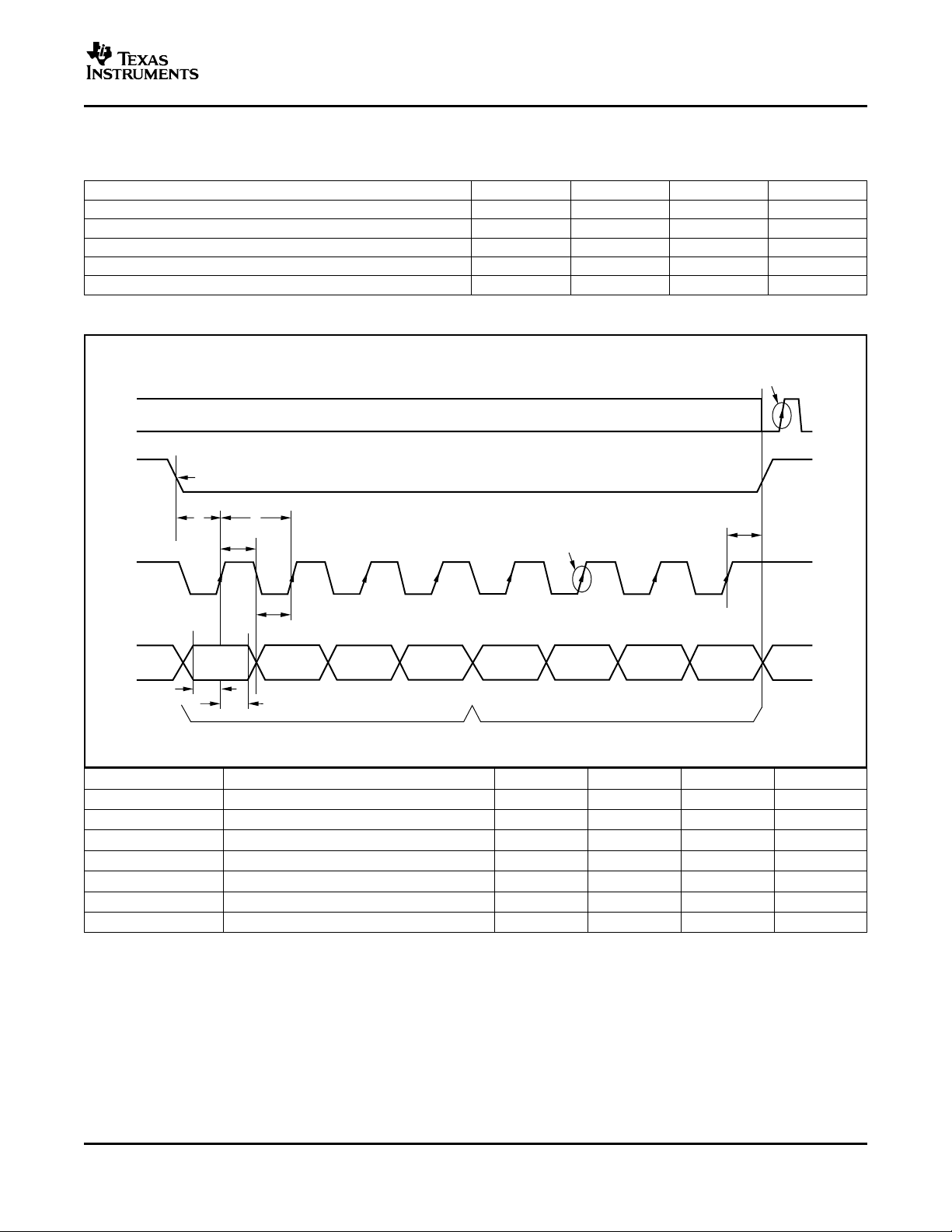
NOTE: Data is shifted in MSB first.
Start Sequence
t
1
t
7
t
6
D7
(MSB)
D6 D5 D4 D3 D2 D1 D0
t
2
t
3
t
4
t
5
CLK
SEN
SCLK
SDATA
Outputs change on
next rising clock edge
after SEN goes high.
Data latched on
each rising edge of SCLK.
SBAS294A – JUNE 2004 – REVISED MARCH 2006
TIMING CHARACTERISTICS (continued)
Typical values at TA= +25°C, AVDD = VDRV = 3.3V, sampling rate and PLL state are as indicated, input clock at 50% duty
cycle, and total capacitive loading = 10pF, unless otherwise noted.
PARAMETER MIN TYP MAX UNITS
t2Data Hold Time 200 250 ns
tDData Latency 6 Clocks
tDR, tDFData Rise/Fall Time 0.5 2 3.5 ns
Data Valid (DV) Duty Cycle 30 45 55 %
tDVInput Clock Rising to DV Fall Edge 200 225 250 ns
SERIAL INTERFACE TIMING
ADS5232
PARAMETER DESCRIPTION MIN TYP MAX UNIT
t
1
t
2
t
3
t
4
t
5
t
6
t
7
Serial CLK Period 50 ns
Serial CLK High Time 20 ns
Serial CLK Low Time 20 ns
Data Setup Time 5 ns
Data Hold Time 5 ns
SEN Fall to SCLK Rise 8 ns
SCLK Rise to SEN Rise 8 ns
Submit Documentation Feedback
9
 Loading...