

Page 1

ADS5120EVM
SBAU078 – JUNE 2002
FEATURES
● FULLY POPULATED EVM
● PROVIDES FAST AND EASY PERFORMANCE
TESTING FOR THE ADS5120
● DIFFERENTIAL TRANSFORMER-COUPLED
INPUT CONFIGURATION FOR EACH CHANNEL
● EXTERNAL REFERENCE OPTION
Please be aware that an important notice concerning availability, standard warranty, and use in critical applications of
Texas Instruments semiconductor products and disclaimers thereto appears at the end of this data sheet.
PRODUCTION DATA information is current as of publication date.
Products conform to specifications per the terms of Texas Instruments
standard warranty. Production processing does not necessarily include
testing of all parameters.
DESCRIPTION
This user’s guide describes the function and operation of the
ADS5120 evaluation module. It is designed for ease of use
when evaluating the high-speed Analog-to-Digital Converter
(ADC) ADS5120. The ADS5120 is an 8-channel, simultaneous sampling 10-bit A/D converter sampling at up to
40MSPS. The evaluation module is completely assembled
and provides a transformer-coupled input configuration for
each of the channels. The ADS5120 operates on a 1.8V
single supply. Optionally, the output logic buffers can be
configured for 3.3V supply.
Copyright © 2002, Texas Instruments Incorporated
www.ti.com
Page 2

OVERVIEW
This preliminary User’s Guide document gives a general
overview of the ADS5120 evaluation module (EVM), and
provides a general description of the features and functions
to be considered while using this module.
The ADS5120EVM provides a platform for evaluating the
ADS5120 ADC under various signal, reference, and supply
conditions.
EVM BASIC FUNCTIONS
Analog inputs to the ADC are provided via eight SMA
connectors (AINA…AINM). The single-ended inputs are transformer coupled and converted into differential signals at the
inputs of the ADC.
The EVM provides a SMA connection for the ADC clock. A
second SMA connector provides a clock to the output connector. This allows the user to provide the required setup and
hold times of the output data with respect to the output clock.
Refer to the Clock input section for proper configuration and
operation.
Digital outputs from the EVM are via four connectors. The
digital lines from the ADC are buffered before going to these
connectors. More information on these connectors can be
found in the ADC Outputs section.
Power connections to the EVM are via banana jack sockets.
Separate sockets are provided for the analog and digital
supplies.
In addition to the internal reference provided by the ADS5120
device, options are provided on the EVM to allow adjustment
of the ADC references via an onboard reference circuit. A
precision-voltage reference source, a resistor network, and
an op amp provide the ADS5120 device reference voltages,
top reference (REFT) and bottom reference (REFB).
POWER REQUIREMENTS
The EVM can be powered directly with a single +1.8V supply
if using internal reference source and +1.8V logic outputs.
+3.3V is required for the DRV
logic outputs. ±5V is required if using the onboard external
reference circuit. Provision has also been made to allow the
EVM to be powered with independent +1.8V analog and
digital supplies to provide higher performance.
power input to provide +3.3V
DD
Voltage Limits
Exceeding the maximum input voltages can damage EVM
components. Under-voltage may cause improper operation
of some or all of the EVM components.
ADS5120EVM OPERATIONAL PROCEDURE
A basic setup procedure that can be used as a board
confidence check is as follows:
1) Verify all jumper settings against the schematic jumper list
in Tables I and II:
JUMPER FUNCTION INSTALLED REMOVED DEFAULT
W3 REFT Feed External Internal Removed
W4 REFB Feed External Internal Removed
R9 ADC Clock Provide Pull-Up No Pull-Up Removed
Termination Option Termination Termination
TABLE I. 2-Pin Jumper List.
2) Connect supplies to the EVM as follows:
+1.8V analog supply to J15 and return to J14.
+1.8V digital supply to J18 and return to J19.
+1.8V driver supply to J21 and return to J22.
3) Switch power supplies ON.
4) Use a function generator with 50Ω output impedance to
input a 40MHz, 1.5V offset, 3Vp-p amplitude square wave
signal into J1 to be used as the ADC clock. The frequency
of the clock must be within the specification for the device
speed grade.
5) Use a function generator with 50Ω output impedance to
input a 40MHz, 1.5V offset, 3Vp-p amplitude square wave
signal into J23 to be used as the buffered output clock.
This signal must be the same frequency and synchronized with the ADC clock.
6) Use a frequency generator with 50Ω output impedance to
input a 1.5MHz, 0V offset, 0.4Vp-p amplitude sine wave
signal into analog input SMA J2. This will provide a
transformer-coupled differential signal to channel A of the
ADC.
7) The digital pattern on the output connector J11 should
now represent a sine wave and can be monitored using a
logic analyzer.
JUMPER FUNCTION LOCATION: PINS 1-2 LOCATION: PINS 3-4 DEFAULT
W32 Transformer Common-Mode Select External Common-Mode Voltage ADC Common-Mode Voltage 2-3
W2 Power-Down Internal Reference Internal Reference Operational Internal Reference Powered Down 1-2
W1 Output Data Enable ADC Outputs Enabled ADC Outputs Tri-Stated 1-2
W22 Bandgap Input Voltage 1.3V REFT Voltage Removed
(power-down reference mode)
SJP1 ADC Duty-Cycle Adjust Enable Enabled Disabled 2-3
TABLE II. 3-Pin Jumper List.
2
www.ti.com
ADS5120EVM
SBAU078
Page 3

CIRCUIT DESCRIPTION
ANALOG INPUTS
The ADC receives differential inputs from eight transformers.
The eight single-ended inputs are provided via SMA connectors J2, J3, J4, J5, J6, J7, J8, and J9. The inputs are ACcoupled and have 50Ω termination resistors.
External Reference Inputs
In addition to being able to use the internal reference of the
ADC, a reference circuit has been included on the EVM.
Using a precision +2.5V low-noise linear regulator as the
primary source, this circuit allows adjustment of the REFT
and REFB signals to the ADC using potentiometers R14 and
R16, respectively. A third source, CML, is also generated to
provide an adjustable common-mode voltage to be used by
the transformers during external reference operation. CML is
adjusted by potentiometer R28. In order to use the ADC with
external references, install jumpers W3 and W4, install jumper
W32 between pins 1 and 2 and jumper W22 between pins 2
and 3. If REFT is set to any voltage other than 1.32V, jumper
W22 should be installed between pins 1 and 2 for optimal
ADC performance. The ranges of the external reference
signals are shown in Table III.
MINIMUM TYPICAL MAXIMUM
SIGNAL VOLTAGE VOLTAGE VOLTAGE
REFT 0.9 1.32 1.6
REFB 0.3 0.781 0.9
CML 0.5 1.05 1.25
SWITCH CHANNEL OPEN CLOSED
SWITCH SWITCH
S1-1 H Operate Standby
S1-2 G Operate Standby
S1-3 F Operate Standby
S1-4 E Operate Standby
S10-1 D Operate Standby
S10-2 C Operate Standby
S10-3 B Operate Standby
S10-4 A Operate Standby
TABLE IV. Standby Switch Operation.
Duty-Cycle Adjust
With jumper SJP1 installed between pins 2 and 3, the
internal duty cycle adjust circuit is disabled. Installing SJP1
between 1 and 2 enables the internal duty cycle adjust
circuit. See device data sheet for details.
Output Enable
With jumper W1 installed between pins 1 and 2, the ADC
data outputs are enabled. The outputs are tri-stated with W1
between pins 2 and 3.
Output Buffer Enables
DIP switch S11 controls the ‘Enable’ function of the
SN74AVC16827 buffers for channels A, B, C, and D. DIP
switch S12 controls the ‘Enable’ function of the
SN74AVC16827 buffers for channels E, F, G, and H. With
the DIP switch set to the open position, the buffer outputs are
enabled. With the switches set to the closed position, the
outputs are tri-stated. Table V shows individual switch operation.
TABLE III. Reference Voltage Adjustment Ranges.
Clock Inputs
The EVM provides separate clock inputs for the ADC (“ADC
Clock”) and the output buffer (“Output Clock”). This allows
the user to send a modified version of the ADC clock
(inverted, delayed, ect.) with the output data to generate the
required setup and hold times for the user’s interface.
An adjustment in the placement of the output clock that
captures the data relative to the ADC clock may be neccessary
depending on the specific timing requirements of the logic
analyzer used. If poor performance is observed, verify the
correct timing.
The ADC clock input is SMA connector J1 and has provisions
for serial and/or parallel termination. The buffered output
clock input is SMA connector J23. The clock inputs should be
50Ω square wave signals, +1.8V or +3.3V referenced to
ground (based on DRV
voltage).
DD
Control Inputs
The ADC has three discrete inputs to control the operation of
the device:
Standby
The ADC has individual standby control inputs for each of the
eight output data buses. These are controlled by the two dip
switches, S1 and S10. Table IV shows switch operation.
SWITCH CHANNEL CLOSED OPEN
SWITCH SWITCH
S11-1 A Tri-State Operate
S11-2 B Tri-State Operate
S11-3 C Tri-State Operate
S11-4 D Tri-State Operate
S12-1 E Tri-State Operate
S12-2 F Tri-State Operate
S12-3 G Tri-State Operate
S12-4 H Tri-State Operate
TABLE V. Output Buffer Switch Operation.
Power-Down Reference
With jumper W2 installed between pins 2 and 3, the ADC
internal reference is disabled and the device is in external
reference mode. The ADC is in internal reference mode with
jumper W2 installed between pins 1 and 2.
Power
Power is supplied to the EVM via banana jack sockets. A
separate connection is provided for a +1.8V analog supply
(J15 and J14), +1.8V digital supply (J18 and J19), +1.8/3.3V
digital driver supply (J21 and J22), and ±5V analog supply
(J16, J17, and J20).
ADS5120EVM
SBAU078
3
www.ti.com
Page 4

ADC Outputs
The data outputs from the ADC are buffered using four
SN74AVC16827 buffers before going to headers J10, J11,
J12, and J13. The ADC and output buffer can provide +1.8V
or +3.3V output levels. This is selected by the voltage placed
at the ADC driver supply (banana jacks J21 and J22). The
standard headers are on a 100-mil grid, which allows for
easy connection to a logic analyzer.
PHYSICAL DESCRIPTION
This section describes the physical characteristics and PCB
layout of the EVM and lists the components used on the
module.
PCB LAYOUT
The EVM is constructed on a 8-layer, 5.45" x 6.30", 0.062inch thick PCB using FR-4 material. A brief description of the
individual layers is shown below. The layer drawings are
attached to the end of this document (Figures 6 - 13).
PARTS LIST
Table VI lists the parts used in constructing the EVM.
4
www.ti.com
ADS5120EVM
SBAU078
Page 5

Value Footprint Qty Part Number Vendor Digi-Key Number REF DES Not Installed
47µF, Tantalum, 10%, 10V 7343 5 10TPA47M SANYO PCS2476CT-ND C171 C175 C179 C183 C187
10µF, 10V, 10% Capacitor 3528 9 GRM42X5R106K10 Murata PCS2106CT-ND C3 C6 C7 C19 C172 C176
0.1µF, 10V, 10% Capacitor 402 47 Panasonic C103-C106 C117 C118 C120
0.1µF, 16V, 10% Capacitor 603 48 ECJ-1VB1C104K Panasonic PCC1762CT-ND C1 C8-C10 C20 C154-C170
` C182 C185 C186 C189
0.01µF, 50V, 10% Capacitor 603 3 AVX PCC1750CT-ND C14 C15 C18
1.0µF, 10V, 10% Capacitor 603 4 AVX PCC1787CT-ND C4 C16 C17 C233
15pF, 16V, 10% Capacitor 603 0 C22-C29
470pF, 16V, 10% Capacitor 603 2 PCC1955CT-ND C2 C11
2.2µF, 16V, 10% Capacitor 805 1 PCC1923CT-ND C5
0.047µF, 16V, 10% 603 3 C12 C13 C21
Ferrite Bead 1206 5 P10437CT-ND FB5-FB9
0Ω Resistor 603 9 R11 R128 R130 R132 R134 R9 R98 R99
10kΩ Resistor, 1/16W, 1% 603 3 P10.0KHCT-ND R17 R18 R29
100Ω Resistor, 1/16W, 1% 603 3 P100YCT-ND R19 R20 R30
100kΩ Resistor, 1/16W, 1% 603 9 R33-R41
1kΩ Resistor, 1/16W, 1% 603 3 P1.00KHCT-ND R8 R13 R101 R145 R147 R149
2.0kΩ Resistor, 1/16W, 1% 603 3 R23 R24 R32
49.9Ω Resistor, 1/16W, 1% 603 13 ERJ-3EKF499R0V Panasonic P499HCT-ND R10 R21 R22 R31 R127 R129
2.49kΩ Resistor, 1/16W, 1% 603 1 ERJ-3EKF249R0V Panasonic P2.49KHCT-ND R15
3.01kΩ Resistor, 1/16W, 1% 603 1 ERJ-3EKF301R0V Panasonic P3.01KHCT-ND R102
4.02kΩ Resistor, 1/16W, 1% 603 0 ERJ-3EKF402R0V Panasonic P4.02KHCT-ND R144 R146 R148
4.7kΩ Resistor, 1/16W, 1% 603 16 ERJ-3EKF4.7KR0V Panasonic P4.7KHCT-ND R1-R7 R89-R97
475Ω Resistor, 1/16W, 1% 603 2 ERJ-3EKF475R0V Panasonic P475HCT-ND R26 R27
6.04kΩ Resistor, 1/16W, 1% 603 1 ERJ-3EKF604KR0V Panasonic P6.04KHCT-ND R12
953Ω Resistor, 1/16W, 1% 603 1 P953GCT-ND R25
1k Pot BOURNS_3296Y 3 3296Y-102 Bourns 3296Y-102-ND R14 R16 R28
Transformer MC_KK81 8 T1-1T-KK81 Mini-Circuits T1-T8
SMA Connectors SMA_Jack 10 713-4339 ALLIED J1-J9 J23 J3
Black Test Point Test_point 5 5011K Keystone TP4-TP8
Red Test Point Test_point 3 5000K Keystone TP1-TP3
2POS_header 2pos_jumper 2 TSW-150-07-L-S Samtec W3 W4
3POS_header 3pos_jumper 4 TSW-150-07-L-S Samtec W1 W2 W22 W32
3POS_JUMPER SMT SJP3 1 SJP1
40-Pin Header 20X2X.1 3 TSW-120-07-L-D Samtec J11-J13
44-Pin Header 22X2X.1 1 J10
Red Banana Jacks BANANA_JACK 5 ST-351A ALLIED J15 J16 J18 J20 J21
Black Banana Jacks BANANA_JACK 4 ST351B ALLIED J14 J17 J19 J22
ADS5120
OPA4227UA 14-SOP(D) 1 OPA4227UA TI U2
TPS79225 5 SOT-23(DBV) 1 TPS79225DBVT TI U3
SN74AVC16827(DGG) 56-TSSOP(DGG) 4 SN74AVC16827(DGG) TI U8-U11
SWITCH 4POS_SMT
Stand Off Hex (1/4 x 0.5
257_S-PBGA(GHK)
SWITCH_4POS_SMT
"
) 4-40 screw 4 1902CK-ND ALLIED
1 ADS5120 TI U1
4 S1 S10 S11 S12
C180 C184 C188
C137 C150-C153 C190-C192
C194 C195 C197-C215 C217
C219-C224 C226 C228
C230 C231
C173 C174 C177 C178 C181
C234-C250
R136 R138 R140 R142
R151 R153 R155
R157 R159
R131 R133 R135 R137 R139
R141 R143
R150 R152 R154
R156 R158
TABLE VI. Parts List.
ADS5120EVM
SBAU078
5
www.ti.com
Page 6

REFT
REFT
J3
REFT
K3
REFB
REFB
J5
REFBK5REFB
L5
REFT
L1
BG
K1
IREFR
K6
CMLL2CML
L3
IREFN
L6
IREFL
M1
CLK
W9
PD_REF
V9
OE
P10
N/CK2N/C
E2
N/C
E1
DCASEL
N2
N/C
W5
N/C
U6
STBYA
W10
STBYBP9STBYC
R9
STBYDU9STBYE
C8
STBYF
B8
STBYG
A8
STBYH
A9
U1A
257BGA_ADS5120
C4
1µF
C5
2.2µF
+5VA
R15
2.49K
R13
1K
R8
1K
1
2
3
R14
1K
R17
10K
C8
0.µF
R19
100
C10
0.1µF
C11
470pF
C12
0.047µF
C9
0.1µF
+5VA
R21
49.9
R23
2.0K
W3
W4
C14
0.01µF
C16
1µF
REFT
R18
10K
R26
475
R25
953
C15
0.01µF
C17
1µF
C1
0.1µF
C2
470pF
–5VA
REFB
EXT_CML
2
3
1
4
11
U2A
OPA4227UA
5
6
7
U2B
OPA4227UA
10
9
8
U2C
OPA4227UA
TP1
TP2
+
C6
10µF
+
C3
10µF
1
2
3
R16
1K
+
C7
10µF
R20
100
C13
0.047µF
R22
49.9
R24
2.0K
0.1%
0.1%
C20
0.1µF
R29
10K
R27
475
1
2
3
R28
1K
+
C19
10µF
R30
100
C21
0.047µF
R31
49.9
R32
2.0K
0.1%
TP3
EN
3
BYPASS
4
OUT
5
GND
2
IN
1
U3
TPS79225
C18
0.01µF
+2.5V
(1.25V TYP)
(0.75V TYP)
(1V TYP)
R1
4.7K 4.7K 4.7K 4.7K 4.7K 4.7K 4.7K 4.7K
R2
R3
R4
R5
R6
R7
1
3
2
W1
1
3
2
W2
DRVDD
DRVDD
CML
CML
1
2
3
4
5
J1
INPUT CLOCK
R10
49.9
CLK
R11
0
R9
0
(1)
DRVDD
12
13
14
U2D
OPA4227UA
R97
R98
0
(1)
1
3
2
W32
EXT_CML
R12
6.19K
R99
0
(1)
ADC_CML
DVDD
1
3
2
W22
R102
3.01K
R101
1K
+5VA
REFT
REFT
C233
1µF
C234
0.1µF
1
2
3
8
4
7
6
5
S1
SWITCH_4POS_SMT
SWITCH_4POS_SMT
1
2
3
8
4
7
6
5
S10
E1
NOTE: (1) Part not installed.
3
1
2
SJP1
R41
100K
AVDD
FIGURE 1. EVM Schematic Diagram (1 of 5).
6
www.ti.com
ADS5120EVM
SBAU078
Page 7

1
2
3
4
5
J3
1
2
3
4
5
J2
R127
49.9
R144
4.02K
(1)
R145
1K
(1)
R130
0
C236
0.1
µF
4
6
3
2
1
T1
T1-6T-KK81_XFMR
AINB+
AINB–
CML
CML
+5VA
C238
0.1
µF
R129
49.9
R146
4.02K
(1)
R147
1K
(1)
R128
0
C237
0.1
µF
4
6
3
2
1
T2
T1-6T-KK81_XFMR
CML
CML
+5VA
AINA+
AINA–
C235
0.1
µF
1
2
3
4
5
J4
C242
0.1
µF
R133
49.9
R150
4.02K
(1)
R151
1K
(1)
R132
0
C241
0.1
µF
4
6
3
2
1
T4
T1-6T-KK81_XFMR
CML
CML
+5VA
AINC–
AINC–
CIN
1
2
3
4
5
J5
C239
0.1
µF
R131
49.9
R148
4.02K
(1)
R149
1K
(1)
R134
0
C240
0.1
µF
4
6
3
2
1
T3
T1-6T-KK81_XFMR
AIND+
AIND–
CML
CML
+5VA
DIN
AIN
BIN
1
2
3
4
5
J6
C246
0.1
µF
R137
49.9
R154
4.02K
(1)
R155
1K
(1)
R136
0
C245
0.1
µF
4
6
3
2
1
T6
T1-6T-KK81–XFMR
CML
CML
+5VA
AINE+
AINE–
EIN
1
2
3
4
5
J7
C243
0.1
µF
R135
49.9
R152
4.02K
(1)
R153
1K
(1)
R138
0
C244
0.1
µF
4
6
3
2
1
T5
T1-6T-KK81_XFMR
AINF+
AINF–
CML
CML
+5VA
FIN
1
2
3
4
5
J8
C250
0.1
µF
R141
49.9
R158
4.02K
R159
1K
(1)
R140
0
C249
0.1
µF
4
6
3
2
1
T8
T1-6T-KK81_XFMR
CML
CML
+5VA
AING+
AING–
GIN
1
2
3
4
5
J9
C247
0.1
µF
R139
49.9
R156
4.02K
(1)
R157
1K
(1)
R142
0
C248
0.1
µF
4
6
3
2
1
T7
T1-6T-KK81_XFMR
AINH+
AINH–
CML
CML
+5VA
HIN
C22
15pF
C24
15pF
C26
15pF
C27
15pF
C29
15pF
C28
15pF
C25
15pF
C23
15pF
NOTE: (1) Part not installed.
AINA+
AINA–
AINC+
AINC–
AINE+
AINE–
AING+
AING–
AINH+
AINH–
AINF+
AINF–
AIND+
AIND–
AINB+
AINB–
FIGURE 2. EVM Schematic Diagram (2 of 5).
ADS5120EVM
SBAU078
www.ti.com
7
Page 8

1
2
3
4
567
8
9
10
111213
14
1516171819
20
21
22
23
24
252627
28
29
303132
3334353637
383940
J11
40PI N_ I DC
AIND+
AIND–
AINC–
AINC+
AINB+
AINB–
AINA–
D9D
N18
D8D
N19
D7D
M18
D6D
M19
D5D
L19
D4D
L18
D3D
K19
D2D
K18
D1D
K15
D0D
K14
AINC+
T1
AINC–
T2
D9C
T17
D8C
U18
D7C
U19
D6C
T18
D5C
T19
D4C
R17
D3C
R18
D2C
R19
D1C
P18
D0C
P19
AIND–
P1
AIND+
P2
U1E
257BGA_ADS 5120
AINA+
AINA+
AINB+
AINB–
AINA–
DRVDD
AINC+
AINC–
AIND+
AIND–
DRVDD
C161
0.1uF
C160
0.1uF
1/OE1
1
1Y1
2
1Y231Y3
5
1Y4
6
1A5
49
1A6
48
1A7471A8
45
1A1
55
1A2541A3521A4
51
1Y5
8
1Y6
9
1Y7101Y8
12
VCC
22
GND
32
2/OE1
28
1/OE2
56
2/OE2
29
1A9
44
2A1
42
2A2
41
2A3402A4382A5
37
2A6
36
2A7
34
1Y9
13
2Y1
15
2Y2162Y3
17
2Y4
19
2Y5202Y6
21
2Y7
23
2A8
33
2A9
31
2Y8242Y9
26
1A10
43
2A10
30
2Y10
27
1Y10
14
VCC
35
VCC
7
VCC
50
GND
11
GND
46
GND
25
GND
39
GND
18
GND
53
GND
4
U8
SN74AVC16827(DGG)
C159
0.1uF
1/OE1
1
1Y1
2
1Y231Y3
5
1Y4
6
1A5491A6
48
1A7
47
1A8
45
1A1
55
1A2541A3
52
1A4
51
1Y5
8
1Y691Y7
10
1Y8
12
VCC
22
GND
32
2/OE1281/OE2
56
2/OE2
29
1A9
44
2A1
42
2A2412A3
40
2A4382A5
37
2A6
36
2A7
34
1Y9
13
2Y1
15
2Y2
16
2Y3172Y4
19
2Y5
20
2Y6
21
2Y7
23
2A8
33
2A9
31
2Y8
24
2Y9
26
1A10
43
2A10
30
2Y10
27
1Y10
14
VCC
35
VCC
7
VCC
50
GND11GND
46
GND25GND
39
GND
18
GND53GND
4
U9
SN74AVC16827(DGG)
C158
0.1uF
DRVDD
DRVDD
C157
0.1
µF
C156
0.1
µF
C155
0.1
µF
C154
0.1
µF
R92
4.7K
R91
4.7K
R90
4.7K
R89
4.7K
DRVDD
A0
A1
A2
A3
A4
A5
A6
A7
A8
A9
B0
B1
B2
B3
B4
B5
B6
B7
B8
B9
C0
C1
C2
C3
C4
C5
C6
C7
C8
C9
D0
D1
D2
D3
D4
D5
D6
D7
D8
D9
AINB–
V4
AINB+
W4
AINA+
U7
AINA–
V7
D9A
W11
D8A
V11
D7A
P11
D6A
R11
D5A
W12
D4A
V12
D3A
W13
D2A
V13
D1A
W14
D0A
V14
D9B
W15
D8B
V15
D7B
W16
D6B
V16
D5B
W17
D4B
V17
D3B
W18
D2B
U17
D1B
V18
D0B
V19
U1D
257BGA_ADS5120
1
234
5
678
9
10
11
121314
15
16
17
181920
212223
242526
27
282930
31
32
333435
36
37
38
394041
42
43
44
J10
44PI N_IDC
1
2
3
4
5
J23
R143
49.9
CHB0
CHB1
CHB2
CHB3
CHB4
CHB5
CHB6
CHB7
CHB8
CHB9
CHA0
CHA1
CHA2
CHA3
CHA4
CHA5
CHA6
CHA7
CHA8
CHA9
CHC0
CHC1
CHC2
CHC3
CHC4
CHC5
CHC6
CHC7
CHC8
CHC9
CHD0
CHD1
CHD2
CHD3
CHD4
CHD5
CHD6
CHD7
CHD8
CHD9
CHA0
CHA1
CHA2
CHA3
CHA4
CHA5
CHA6
CHA7
CHA8
CHA9
123
456
7
8
91011
12
13
141516
17
18
192021
222324
252627
28
293031
32
33
343536
37
38
39
40
J12
40PI N_ I DC
123
4
567
8
91011
12
131415
161718
19
202122
23
242526
272829
30
31
323334
353637
38
39
40
J13
40PI N_ I DC
CHD0
CHD1
CHD2
CHD3
CHD4
CHD5
CHD6
CHD7
CHD8
CHD9
CHE0
CHE1
CHE2
CHE3
CHE4
CHE5
CHE6
CHE7
CHE8
CHE9
CHF(0..9)
CHF0
CHF1
CHF2
CHF3
CHF4
CHF5
CHF6
CHF7
CHF8
CHF9
CHE(0..9)
CHH(0..9)
CHG(0..9)
CHH0
CHH1
CHH2
CHH3
CHH4
CHH5
CHH6
CHH7
CHH8
CHH9
CHG0
CHG1
CHG2
CHG3
CHG4
CHG5
CHG6
CHG7
CHG8
CHG9
CHC0
CHC1
CHC2
CHC3
CHC4
CHC5
CHC6
CHC7
CHC8
CHC9
CHB0
CHB1
CHB2
CHB3
CHB4
CHB5
CHB6
CHB7
CHB8
CHB9
1
2
3
8
4
7
6
5
S11
SWITCH_4POS_SMT
CLOCK
OUTPUT
Enable A
Enable B
Enable C
Enable D
R33
100k
R34
100k
R35
100k
R36
100k
FIGURE 3. EVM Schematic Diagram (3 of 5).
8
www.ti.com
ADS5120EVM
SBAU078
Page 9

AINE–
AINE+
AINF–
AINF+
AINH
AINH+
AING
AING+
DRVDD
U10
SN74AVC16827(DGG)
R96
4.7K
7
50
55
54
52
51
49
48
47
45
44
43
42
41
40
38
37
36
34
33
31
1
56
28
29
53
4
DRVDD
SN74AVC16827(DGG)
7
50
55
54
52
51
49
48
47
45
44
43
42
41
40
38
37
36
34
33
31
1
56
28
29
53
4
VCC
VCC
VCC
VCC
1A1
1A2
1A3
1A4
1A5
1A6
1A7
1A8
1A9
1A10
1Y10
2A1
2A2
2A3
2A4
2A5
2A6
2A7
2A8
2A9
2A10302Y10
1/OE1
1/OE2
GND
2/OE1
GND
2/OE2
GND
GND
GND
GND
GND
GND
U11
VCC
VCC
VCC
VCC
1A1
1A2
1A3
1A4
1A5
1A6
1A7
1A8
1A9
1A10
1Y10
2A1
2A2
2A3
2A4
2A5
2A6
2A7
2A8
2A9
2A10302Y10
1/OE1
1/OE2
GND
2/OE1
GND
2/OE2
GND
GND
GND
GND
GND
GND
U1F
G2
AINE-
G3
AINE+
D2
AINF-
D1
AINF+
DRVDD
SWITCH_4POS_SM T
A6
AINH-
B6
AINH+
B4
AING-
A4
AING+
257BGA_ADS5120
S12
1
2
3
4
257BGA_ADS5120
J19
D9E
J18
D8E
J17
D7E
J15
D6E
H19
D5E
H18
D4E
G19
D3E
G18
D2E
F19
D1E
F18
D0E
E19
D9F
E18
D8F
D19
D7F
D18
D6F
C19
D5F
C18
D4F
B19
D3F
C17
D2F
B18
D1F
A18
D0F
8
7
6
5
R37
R38
R39
100k
100k
U1G
D0H
D1H
D2H
D3H
D4H
D5H
D6H
D7H
D8H
D9H
D0G
D1G
D2G
D3G
D4G
D5G
D6G
D7G
D8G
D9G
100k
C10
B10
A10
C11
B11
A11
A12
B12
C12
A13
A14
B14
C14
A15
B15
E14
C15
A16
B16
A17
R40
100k
E9
E8
E7
E6
E5
E4
E3
E2
E1
E0
F9
F8
F7
F6
F5
F4
F3
F2
F1
F0
R94
R93
4.7K
4.7K
R95
4.7K
H0
H1
H2
H3
H4
H5
H6
H7
H8
H9
G0
G1
G2
G3
G4
G5
G6
G7
G8
G9
–
AINE
AINE+
–
AINF
AINF+
Enable E
Enable F
Enable G
Enable H
–
AINH
–
AINH+
–
AING
–
AING+
DRVDD
C165
C164
C163
C162
0.1uF
DRVDD
C166
0.1uF
0.1uF
0.1uF
CHE 9
CHE 8
CHE 7
CHE 6
CHE 5
CHE 4
CHE 3
CHE 2
CHE 1
CHE 0
CHF9
CHF8
CHF7
CHF6
CHF5
CHF4
CHF3
CHF2
CHF1
CHF0
C167
CHH0
CHH1
CHH2
CHH3
CHH4
CHH5
CHH6
CHH7
CHH8
CHH9
CHG0
CHG1
CHG2
CHG3
CHG4
CHG5
CHG6
CHG7
CHG8
CHG9
22
35
2
1Y1
3
1Y2
5
1Y3
6
1Y4
8
1Y5
9
1Y6
10
1Y7
12
1Y8
13
1Y9
14
15
2Y1
16
2Y2
17
2Y3
19
2Y4
20
2Y5
21
2Y6
23
2Y7
24
2Y8
26
2Y9
27
11
46
18
39
25
32
22
35
2
1Y1
3
1Y2
5
1Y3
6
1Y4
8
1Y5
9
1Y6
10
1Y7
12
1Y8
13
1Y9
14
15
2Y1
16
2Y2
17
2Y3
19
2Y4
20
2Y5
21
2Y6
23
2Y7
24
2Y8
26
2Y9
27
11
46
18
39
25
32
0.1uF
C168
0.1uF
0.1uF
CHE (0..9)
CHF(0..9)
C169
0.1uF
CHH(0..9)
CHG(0..9)
FIGURE 4. EVM Schematic Diagram (4 of 5).
ADS5120EVM
SBAU078
9
www.ti.com
Page 10

C173
0.1uF
AVDD
ADC Analog Supply ( + 1. 8V)
C181
0.1uF
DVDD
ADC Digital Supply (+1.8V)
C189
0.1uF
DRVDD
ADC Driver Supply (+1.8V/3.3v)
C177
0.1uF
+5VA
Analog Supply (+/-5volts) for Ext. Components
C185
0.1uF
-5VA
+1.8VA- PS
+1.8VD-PS
+1.8V/+3.3VD- PS
+5VA-PS
-5VA- PS
J15
BANANA_JACK
J14
BANANA_JACK
FB5
FB7
FB9
FB8
FB6
J18
BANANA_JACK
J19
BANANA_JACK
J20
BANANA_JACK
J17
BANANA_JACK
J16
BANANA_JACK
J21
BANANA_JACK
J22
BANANA_JACK
+
C172
10 uF
+
C171
47 uF
+
C180
10 uF
+
C188
10 uF
+
C176
10 uF
+
C184
10 uF
+
C179
47 uF
+
C187
47 uF
+
C175
47 uF
+
C183
47 uF
C170
0.1uF
C178
0.1uF
C186
0.1uF
C182
0.1uF
C174
0.1uF
AGND
B5
DGND
B2
AGND
F7
DGND
B7
AGND
A5
AGND
N5
AGND
G1
AGND
G5
AGND
E3
AGND
B9
AGND
E7
AGND
C1
AGND
M2
AGND
G6
AGND
J2
AGND
N6
AGND
J1
DGND
H2
AGND
C9
DGND
H1
AGND
C5
AGND
A3
AGND
H6
AGND
P8
DGND
W8
AGND
R1
DGND
V8
AGND
R2
DGND
A2
AGND
R3
DGND
A7
AGND
R7
DGND
B1
AGND
U1
DGND
B3
AGND
U5
DGND
W2
AGND
U10
DGND
V2
AGND
V5
DGND
V1
AGND
V10
DGND
U2
AGND
W3
DGND
N1
AGND
W7
DGND
M6
DRGND
U11
DRGND
U12
DRGND
U13
DRGND
U14
DRGND
U15
DRGND
U16
DRGND
N15
DRGND
M14
DRGND
N17
DRGND
M15
DRGND
M17
DRGND
L17
DRGND
H17
DRGND
G17
DRGND
G15
DRGND
G14
DRGND
F14
DRGND
F15
DRGND
F13
DRGND
E13
DRGND
C13
DRGND
B13
DRGND
F11
DRGND
F10
U1C
257BGA_ADS5120
DVDD
DRVDD
AVDD
DVDD
C103
0.1uF
C104
0.1uF
C105
0.1uF
C106
0.1uF
C117
0.1uF
C118
0.1uF
C120
0.1uF
C137
0.1uF
C150
0.1uF
C151
0.1uF
C152
0.1uF
C153
0.1uF
C190
0.1uF
C191
0.1uF
C192
0.1uF
C194
0.1uF
C195
0.1uF
DRVDD
C198
0.1uF
C200
0.1uF
C202
0.1uF
C204
0.1uF
C206
0.1uF
C208
0.1uF
C210
0.1uF
C212
0.1uF
C214
0.1uF
C220
0.1uF
C222
0.1uF
C224
0.1uF
C226
0.1uF
C228
0.1uF
C230
0.1uF
C231
0.1uF
AVDD
C197
0.1uF
C199
0.1uF
C201
0.1uF
C203
0.1uF
C205
0.1uF
C207
0.1uF
C209
0.1uF
C211
0.1uF
C213
0.1uF
C215
0.1uF
C217
0.1uF
C219
0.1uF
C221
0.1uF
C223
0.1uF
DVDD
D3
DVDD
C2
AVDD
P3
AVDDE6AVDD
F1
AVDD
P5
DVDD
H3
DVDDH5DVDD
M3
DVDD
M5
DVDD
T3
DVDDU3DVDD
U4
DVDD
V3
DVDD
C4
DVDD
C3
DVDD
E8
DVDD
F8
DVDD
R8
DVDD
U8
AVDD
P6
AVDD
F6
AVDDF5AVDD
F3
AVDD
F2
AVDD
P7
AVDD
R6
AVDD
W6
AVDD
C7
AVDD
C6
AVDD
N3
AVDD
J6
DVDD
F17
DVDD
L15
DRVDD
P12
DRVDD
R10
DRVDD
P15
DVDD
P17
DRVDD
P14
DRVDD
N14
DVDD
P13
DRVDD
K17
DRVDD
L14
DVDD
J14
DRVDD
H14
DRVDD
H15
DRVDD
E17
DRVDD
D17
DRVDD
C16
DRVDD
B17
DVDD
F12
DVDD
E12
DRVDD
E11
DRVDD
E10
DRVDD
F9
DRVDD
E9
DRVDD
R12
DVDD
R13
DRVDD
R14
AVDD
V6
U1B
257BGA_ADS5120
TP5
TP6
TP7
TP8
TP4
FIGURE 5. EVM Schematic Diagram (5 of 5).
10
www.ti.com
ADS5120EVM
SBAU078
Page 11

FIGURE 6. EVM Layer 1: Top Layer with Silk-Screen.
ADS5120EVM
SBAU078
11
www.ti.com
Page 12

FIGURE 7. EVM Layer 2: Ground Plane I.
12
www.ti.com
ADS5120EVM
SBAU078
Page 13

FIGURE 8. EVM Layer 3: Inner Layer I.
ADS5120EVM
SBAU078
13
www.ti.com
Page 14

FIGURE 9. EVM Layer 4: Split Power Plane I.
14
www.ti.com
ADS5120EVM
SBAU078
Page 15

FIGURE 10. EVM Layer 5: Inner Layer II.
ADS5120EVM
SBAU078
15
www.ti.com
Page 16
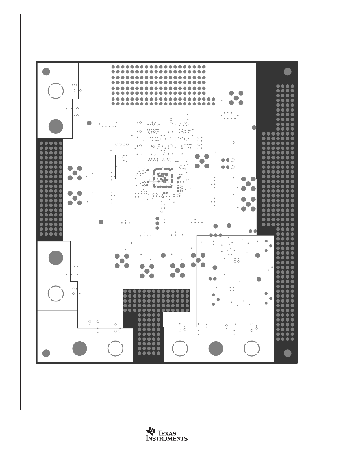
FIGURE 11. EVM Layer 6: Split Power Plane II.
16
www.ti.com
ADS5120EVM
SBAU078
Page 17

FIGURE 12. EVM Layer 7: Ground Plane II.
ADS5120EVM
SBAU078
17
www.ti.com
Page 18

FIGURE 13. EVM Layer 8: Bottom Layer with Silk Screen.
18
www.ti.com
ADS5120EVM
SBAU078
Page 19

EVM IMPORTANT NOTICE
Texas Instruments (TI) provides the enclosed product(s) under the following conditions:
This evaluation kit being sold by TI is intended for use for ENGINEERING DEVELOPMENT OR EV ALUATION
PURPOSES ONL Y and is not considered by TI to be fit for commercial use. As such, the goods being provided
may not be complete in terms of required design–, marketing–, and/or manufacturing–related protective
considerations, including product safety measures typically found in the end product incorporating the goods.
As a prototype, this product does not fall within the scope of the European Union directive on electromagnetic
compatibility and therefore may not meet the technical requirements of the directive.
Should this evaluation kit not meet the specifications indicated in the EVM User’s Guide, the kit may be returned
within 30 days from the date of delivery for a full refund. THE FOREGOING WARRANTY IS THE EXCLUSIVE
WARRANTY MADE BY SELLER TO BUYER AND IS IN LIEU OF ALL OTHER WARRANTIES, EXPRESSED,
IMPLIED, OR STATUTORY, INCLUDING ANY WARRANTY OF MERCHANTABILITY OR FITNESS FOR ANY
PARTICULAR PURPOSE.
The user assumes all responsibility and liability for proper and safe handling of the goods. Further, the user
indemnifies TI from all claims arising from the handling or use of the goods. Please be aware that the products
received may not be regulatory compliant or agency certified (FCC, UL, CE, etc.). Due to the open construction
of the product, it is the user’s responsibility to take any and all appropriate precautions with regard to electrostatic
discharge.
EXCEPT TO THE EXTENT OF THE INDEMNITY SET FORTH ABOVE, NEITHER P ARTY SHALL BE LIABLE
TO THE OTHER FOR ANY INDIRECT, SPECIAL, INCIDENTAL, OR CONSEQUENTIAL DAMAGES.
TI currently deals with a variety of customers for products, and therefore our arrangement with the user is not
exclusive.
TI assumes no liability for applications assistance, customer product design, software performance, or
infringement of patents or services described herein.
Please read the EVM User’s Guide and, specifically, the EVM Warnings and Restrictions notice in the EVM
User’s Guide prior to handling the product. This notice contains important safety information about temperatures
and voltages. For further safety concerns, please contact the TI application engineer.
Persons handling the product must have electronics training and observe good laboratory practice standards.
No license is granted under any patent right or other intellectual property right of TI covering or relating to any
machine, process, or combination in which such TI products or services might be or are used.
Mailing Address:
Texas Instruments
Post Office Box 655303
Dallas, Texas 75265
ADS5120EVM
SBAU078
Copyright 2002, Texas Instruments Incorporated
19
www.ti.com
Page 20

EVM WARNINGS AND RESTRICTIONS
It is important to operate this EVM within the input voltage range of ≤ 3.3V and the output
voltage range of ≤ 3.3V.
Exceeding the specified input range may cause unexpected operation and/or irreversible
damage to the EVM. If there are questions concerning the input range, please contact a TI
field representative prior to connecting the input power.
Applying loads outside of the specified output range may result in unintended operation and/or
possible permanent damage to the EVM. Please consult the EVM User’s Guide prior to
connecting any load to the EVM output. If there is uncertainty as to the load specification,
please contact a TI field representative.
During normal operation, some circuit components may have case temperatures greater than
60°C. The EVM is designed to operate properly with certain components above 60°C as long
as the input and output ranges are maintained. These components include but are not limited
to linear regulators, switching transistors, pass transistors, and current sense
resistors. These types of devices can be identified using the EVM schematic located in the
EVM User’s Guide. When placing measurement probes near these devices during operation,
please be aware that these devices may be very warm to the touch.
Mailing Address:
Texas Instruments
Post Office Box 655303
Dallas, Texas 75265
Copyright 2002, Texas Instruments Incorporated
20
www.ti.com
ADS5120EVM
SBAU078
Page 21

IMPORTANT NOTICE
Texas Instruments Incorporated and its subsidiaries (TI) reserve the right to make corrections, modifications, enhancements,
improvements, and other changes to its products and services at any time and to discontinue any product or service without notice.
Customers should obtain the latest relevant information before placing orders and should verify that such information is current and
complete. All products are sold subject to TI’s terms and conditions of sale supplied at the time of order acknowledgment.
TI warrants performance of its hardware products to the specifications applicable at the time of sale in accordance with TI’s
standard warranty. Testing and other quality control techniques are used to the extent TI deems necessary to support this
warranty. Except where mandated by government requirements, testing of all parameters of each product is not necessarily
performed.
TI assumes no liability for applications assistance or customer product design. Customers are responsible for their products and
applications using TI components. To minimize the risks associated with customer products and applications, customers should
provide adequate design and operating safeguards.
TI does not warrant or represent that any license, either express or implied, is granted under any TI patent right, copyright, mask
work right, or other TI intellectual property right relating to any combination, machine, or process in which TI products or services
are used. Information published by TI regarding third-party products or services does not constitute a license from TI to use such
products or services or a warranty or endorsement thereof. Use of such information may require a license from a third party under
the patents or other intellectual property of the third party, or a license from TI under the patents or other intellectual property of TI.
Reproduction of information in TI data books or data sheets is permissible only if reproduction is without alteration and is
accompanied by all associated warranties, conditions, limitations, and notices. Reproduction of this information with alteration is an
unfair and deceptive business practice. TI is not responsible or liable for such altered documentation.
Resale of TI products or services with statements different from or beyond the parameters stated by TI for that product or service
voids all express and any implied warranties for the associated TI product or service and is an unfair and deceptive business
practice. TI is not responsible or liable for any such statements.
TI products are not authorized for use in safety-critical applications (such as life support) where a failure of the TI product would
reasonably be expected to cause severe personal injury or death, unless officers of the parties have executed an agreement
specifically governing such use. Buyers represent that they have all necessary expertise in the safety and regulatory ramifications
of their applications, and acknowledge and agree that they are solely responsible for all legal, regulatory and safety-related
requirements concerning their products and any use of TI products in such safety-critical applications, notwithstanding any
applications-related information or support that may be provided by TI. Further, Buyers must fully indemnify TI and its
representatives against any damages arising out of the use of TI products in such safety-critical applications.
TI products are neither designed nor intended for use in military/aerospace applications or environments unless the TI products are
specifically designated by TI as military-grade or "enhanced plastic." Only products designated by TI as military-grade meet military
specifications. Buyers acknowledge and agree that any such use of TI products which TI has not designated as military-grade is
solely at the Buyer's risk, and that they are solely responsible for compliance with all legal and regulatory requirements in
connection with such use.
TI products are neither designed nor intended for use in automotive applications or environments unless the specific TI products
are designated by TI as compliant with ISO/TS 16949 requirements. Buyers acknowledge and agree that, if they use any
non-designated products in automotive applications, TI will not be responsible for any failure to meet such requirements.
Following are URLs where you can obtain information on other Texas Instruments products and application solutions:
Products Applications
Amplifiers amplifier.ti.com Audio www.ti.com/audio
Data Converters dataconverter.ti.com Automotive www.ti.com/automotive
DSP dsp.ti.com Broadband www.ti.com/broadband
Interface interface.ti.com Digital Control www.ti.com/digitalcontrol
Logic logic.ti.com Military www.ti.com/military
Power Mgmt power.ti.com Optical Networking www.ti.com/opticalnetwork
Microcontrollers microcontroller.ti.com Security www.ti.com/security
RFID www.ti-rfid.com Telephony www.ti.com/telephony
Low Power www.ti.com/lpw Video & Imaging www.ti.com/video
Wireless
Mailing Address: Texas Instruments, Post Office Box 655303, Dallas, Texas 75265
Wireless www.ti.com/wireless
Copyright © 2007, Texas Instruments Incorporated
Page 22

Mouser Electronics
Authorized Distributor
Click to View Pricing, Inventory, Delivery & Lifecycle Information:
Texas Instruments:
ADS5120EVM
 Loading...