

Page 1

ADS1x9xECG-FE Demonstration Kit
User's Guide
Literature Number: SLAU384A
December 2011–Revised April 2012
Page 2

Contents
1 ADS1x9xECG-FE ................................................................................................................. 5
1.1 Important Disclaimer Notice ............................................................................................ 5
2 Overview ............................................................................................................................ 6
2.1 Introduction ............................................................................................................... 6
2.2 Features Supported in this Version ................................................................................... 6
3 Software Installation ............................................................................................................ 7
3.1 Minimum Requirements ................................................................................................ 7
3.2 Installing the Software (PC application) .............................................................................. 7
3.3 Installing the USB Drivers ............................................................................................ 12
4 Running the Software ........................................................................................................ 16
4.1 Overview of the Features ............................................................................................. 17
5 ADS1x9xECG-FE Hardware Introduction .............................................................................. 27
5.1 Power Supply ........................................................................................................... 27
5.2 Clock ..................................................................................................................... 28
5.3 Memory .................................................................................................................. 28
5.4 Accessing ADS1x9x Digital Signals ................................................................................. 28
5.5 GPIO Test Points ...................................................................................................... 28
5.6 Analog Inputs ........................................................................................................... 28
5.7 USB Interface ........................................................................................................... 29
5.8 Onboard Key Interface ................................................................................................ 29
5.9 Visual Indication ........................................................................................................ 30
6 Evaluation of ECG and Respiration Specific Functions .......................................................... 30
6.1 Evaluation Mode (Analysis Mode) ................................................................................... 31
6.2 Live Data Streaming Mode ........................................................................................... 32
7 USB-Based Firmware Upgrade ............................................................................................ 37
8 Connector Interface ........................................................................................................... 38
8.1 DB9 ECG Electrode Connector ...................................................................................... 39
8.2 USB Mini Connector ................................................................................................... 39
Appendix A ECG Cable Details .................................................................................................... 40
Appendix B ADS1x9x EVM Bill of Materials (BOM) ........................................................................ 41
Appendix C PCB Layout and Schematics ..................................................................................... 46
C.1 PCB Layout ............................................................................................................ 46
C.2 Schematics ............................................................................................................ 49
2
Table of Contents SLAU384A–December 2011–Revised April 2012
Copyright © 2011–2012, Texas Instruments Incorporated
Submit Documentation Feedback
Page 3

www.ti.com
1 ADS1x9xECG-FE Demonstration Kit..................................................................................... 6
2 PC Application Installation Screen 1 ..................................................................................... 8
3 PC Application Installation Screen 2 ..................................................................................... 8
4 PC Application Installation Screen 3 ..................................................................................... 9
5 PC Application Installation Screen 4 ..................................................................................... 9
6 PC Application Installation Screen 5.................................................................................... 10
7 PC Application Installation Screen 6.................................................................................... 10
8 PC Application Installation Screen 7.................................................................................... 11
9 PC Application Installation Screen 8.................................................................................... 11
10 PC Application Installation Screen 9.................................................................................... 12
11 PC Application Installation Screen 10 .................................................................................. 12
12 Hardware Wizard Screen 1 .............................................................................................. 13
13 Hardware Wizard Screen 2 .............................................................................................. 13
14 Hardware Wizard Screen 3 .............................................................................................. 14
15 Hardware Wizard Screen 4 .............................................................................................. 14
16 Hardware Wizard Screen 5 .............................................................................................. 15
17 Hardware Wizard Screen 6 .............................................................................................. 15
18 Device Manager Screen.................................................................................................. 16
19 EVM not connected Error Message..................................................................................... 16
20 Register Configuration - Channel Registers ........................................................................... 17
21 Register Configuration – LOFF and RLD............................................................................... 18
22 Register Configuration – GPIO .......................................................................................... 18
23 Register Configuration – Respiration Registers....................................................................... 19
24 Register Configuration – Register Map................................................................................. 19
25 PC Application Analysis – SCOPE...................................................................................... 20
26 PC Application Analysis - Histogram.................................................................................... 21
27 PC Application Analysis - FFT........................................................................................... 22
28 PC Application Analysis – ECG ......................................................................................... 23
29 PC Application Analysis – ADS1292R Respiration (Low Pass Filter Enabled) ................................... 23
30 PC Application Save ...................................................................................................... 24
31 PC Application Live ECG for ADS1292R............................................................................... 25
32 PC Application Live Respiration Channel.............................................................................. 26
33 Simulator Connection..................................................................................................... 29
34 Switch Positions ........................................................................................................... 30
35 Firmware Architecture..................................................................................................... 31
36 Evaluation Mode Data Flow for ADS1292R............................................................................ 32
37 Live Data Stream Mode Data Flow for ADS1292R ................................................................... 33
38 Frequency Response for the IIR Filter.................................................................................. 34
39 Frequency Response for the MBF Filter (Full View).................................................................. 34
40 Frequency Response for the MBF Filter (50Hz Notch)............................................................... 35
41 Frequency Response for the MBF Filter (Sharp cut off Around 150Hz) ........................................... 35
42 Frequency Response for the Band Pass Filter ........................................................................ 35
43 PC Application Firmware Upgrade - 1.................................................................................. 37
44 PC Application Firmware Upgrade - 2.................................................................................. 38
45 PC Application Firmware Upgrade - 3.................................................................................. 38
46 DB9 ECG Connector Pin Outs........................................................................................... 39
47 USB Mini Connector Pin Outs........................................................................................... 39
List of Figures
SLAU384A–December 2011–Revised April 2012 List of Figures
Submit Documentation Feedback
3
Copyright © 2011–2012, Texas Instruments Incorporated
Page 4

www.ti.com
48 ECG Cable Drawing....................................................................................................... 40
49 Top Layer Placement ..................................................................................................... 47
50 Bottom Layer Placement ................................................................................................. 48
4
List of Figures SLAU384A–December 2011–Revised April 2012
Copyright © 2011–2012, Texas Instruments Incorporated
Submit Documentation Feedback
Page 5

This user's guide describes the characteristics, operation, and use of the ADS1x9xECG-FE. This
demonstration kit models the ADS1192, ADS1292 and ADS1292R. The family of devices are two-channel,
16/24-bit, low-power, integrated analog front-end (AFE) designed for portable electrocardiogram (ECG)
and respiration applications. The ADS1x9xECG-FE is intended for prototyping and evaluation. This user's
guide includes a complete circuit description, schematic diagram, and Bill of Materials.
1 ADS1x9xECG-FE
1.1 Important Disclaimer Notice
NOTICE: The ADS1x9x demonstration kits are intended for feasibility and evaluation testing only in
laboratory and development environments. This product is not for diagnostic use. This product is
not for use with a defibrillator:
• The ADS1x9xECG-FE to be used only under these conditions:
– The ADS1x9xECG-FE demonstration kit must not be used for diagnostic purposes.
–
– The ADS1x9xECG-FE demonstration kit is intended solely for evaluation and development
purposes. It is not intended for use and may not be used as all or part of an end equipment
product.
– The ADS1x9xECG-FE demonstration kit should be used solely by qualified engineers and
technicians who are familiar with the risks associated with handling electrical and mechanical
components, systems and subsystems.
– You are responsible for the safety of you and your employees and contractors when using or
handling the ADS1x9x demonstration kit. Furthermore, you are fully responsible for the contact
interface between the human body and electronics; consequently, you are responsible for
preventing electrical hazards such as shock, electrostatic discharge, and electrical overstress of
electric circuit components.
User's Guide
SLAU384A–December 2011–Revised April 2012
ADS1x9xECG-FE Demonstration Kit
Pentium, Celeron are trademarks of Intel Corporation.
Windows is a registered trademark of Microsoft Corporation.
All other trademarks are the property of their respective owners.
SLAU384A–December 2011–Revised April 2012 ADS1x9xECG-FE Demonstration Kit
Submit Documentation Feedback
5
Copyright © 2011–2012, Texas Instruments Incorporated
Page 6

Overview
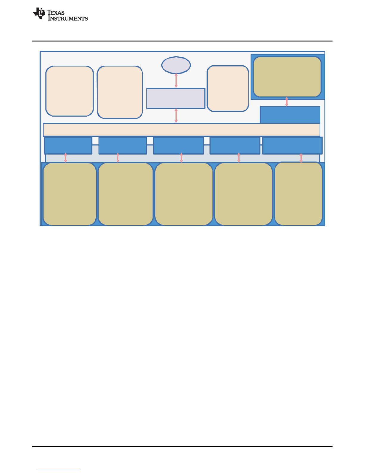
2 Overview
2.1 Introduction
NOTE: From this point on, unless otherwise noted, ADS1x9x refers to ADS1192, ADS1292 and
ADS1292R based demonstration kits.
This user’s guide describes ADS1x9x software and hardware. The appendix contains the Bill of Materials
and schematic design. The demonstration board shown in Figure 1 is provided to accomodate evaluation
and system development activities related to ADS1x9x devices.
www.ti.com
Figure 1. ADS1x9xECG-FE Demonstration Kit
The hardware is designed so all of the following ECG front end devices can be evaluated:
1. ADS1292 – 2 channels at 24 bits
2. ADS1292R – 2 channel at 24 bit with respiration
3. ADS1291 – 1 channel at 24 bit
4. ADS1191 – 1 channel at 16 bit
5. ADS1192 – 2 channel at 16 bit
The board can be assembled with any of these chips. ADS1292, ADS1292R and ADS1192 demonstration
kits are available. The MSP430 firmware and PC application are designed to automatically detect the
installed part and configure to accommodate the part.
Throughout this document, the term demonstration kit is synonymous with the ADS1x9xECG-FE.
2.2 Features Supported in this Version
1. Four electrode ECG cable support
2. View six ECG Leads: Lead I, Lead II, Lead III, Lead aVR, Lead aVL, Lead aVF and respiration channel
(ADS1292R only) .
3. Two modes of operation: Evaluation and Live ECG / Respiration
4. Acquire data at up to 8 kHz in Evaluation mode
5. Current based Lead off detection
6. USB based power and PC application connectivity
7. Access to all ADS1x9x registers via an easy to use GUI.
6
ADS1x9xECG-FE Demonstration Kit SLAU384A–December 2011–Revised April 2012
Copyright © 2011–2012, Texas Instruments Incorporated
Submit Documentation Feedback
Page 7

www.ti.com
8. Built-in time domain, histogram, FFT and ECG / Resp related analysis on the PC application
9. Live ECG with heart rate calculation.
10. Live Respiration wave with respiration rate calculation
11. USB based firmware upgrade option
12. MSP430 Firmware debugging using ez430 USB emulator
3 Software Installation
3.1 Minimum Requirements
Before installing the software, verify that your PC meets the minimum requirements outlined in this section
3.1.1 Required Setup for ADS1x9xECG-FE Demo Software
• IBM PC-compatible computer
• Pentium™ III/ Celeron™ 866 MHz or equivalent processor
• Minimum 256 MB of RAM (512 MB or greater recommended)
• Hard disk drive with at least 200 MB free space
• Microsoft Windows®XP SP2 operating system or Windows 7 operating system
• 1280 × 1024 or greater display screen resolution
3.1.2 Additional Requirements for use with Hardware
• ADS1x9xECG-FE Demonstration Kit
• USB to mini USB cable
• DB9 ECG Cable
Software Installation
3.2 Installing the Software (PC application)
Before installing the software, make sure the ADS1x9xECG-FE is NOT connected to the PC. If using a
machine with Windows 7, we recommend having administrator rights to avoid problems during installation.
Unzip the installer file, and then find and double click setup.exe to install the software. Unless otherwise
specified during the install process, the software installs at C:\Program Files\Texas
Instruments\ADS1x9xEVM. It creates a program menu item ADS1x9xEVM under Programs → Texas
Instruments → ADS1x9xevm to execute the software. The following steps ensure proper installation of the
PC application.
SLAU384A–December 2011–Revised April 2012 ADS1x9xECG-FE Demonstration Kit
Submit Documentation Feedback
7
Copyright © 2011–2012, Texas Instruments Incorporated
Page 8

Software Installation
Click on setup.exe and the following screen appears. Click “Next”
www.ti.com
Figure 2. PC Application Installation Screen 1
Accept the License Agreement and click “Next”.
Figure 3. PC Application Installation Screen 2
8
ADS1x9xECG-FE Demonstration Kit SLAU384A–December 2011–Revised April 2012
Copyright © 2011–2012, Texas Instruments Incorporated
Submit Documentation Feedback
Page 9

www.ti.com
Accept the License Agreement and click “Next”.
Software Installation
Figure 4. PC Application Installation Screen 3
The LabVIEW application software is installed now. Click “Next” to install the Microsoft C++ 2008
Redistributable Package (x86).
Figure 5. PC Application Installation Screen 4
SLAU384A–December 2011–Revised April 2012 ADS1x9xECG-FE Demonstration Kit
Submit Documentation Feedback
9
Copyright © 2011–2012, Texas Instruments Incorporated
Page 10

Software Installation
If your system already has the Microsoft C++ 2008 Redistributable Package (x86) installed, then the
following screen appears. Click “Cancel” to proceed.
www.ti.com
Figure 6. PC Application Installation Screen 5
Click “Finish” to complete the installation procedure.
Figure 7. PC Application Installation Screen 6
10
ADS1x9xECG-FE Demonstration Kit SLAU384A–December 2011–Revised April 2012
Copyright © 2011–2012, Texas Instruments Incorporated
Submit Documentation Feedback
Page 11

www.ti.com
If your system does not have the Microsoft C++ 2008 Redistributable Package (x86) installed, then the
following screen appears. Click “Next”.
Software Installation
Figure 8. PC Application Installation Screen 7
Accept the license terms and click “Install”.
Figure 9. PC Application Installation Screen 8
SLAU384A–December 2011–Revised April 2012 ADS1x9xECG-FE Demonstration Kit
Submit Documentation Feedback
11
Copyright © 2011–2012, Texas Instruments Incorporated
Page 12

Software Installation
Click “Finish” to complete the installation.
The following screen might appear for the first time installation. Restart the machine.
www.ti.com
Figure 10. PC Application Installation Screen 9
Figure 11. PC Application Installation Screen 10
The PC application is now ready to use.
3.3 Installing the USB Drivers
The communication interface between the ADS1x9xECG-FE board and PC is through USB using CDC
profile. A onetime installation of the USB driver is required for the communication between ADS1x9xECGFE and PC application.
The following steps will ensure proper installation of the USB drivers.
1. Plug-in USB to mini USB cable to P1 of ADS1x9xECG-FE and the other end to the USB port on the
PC.
2. The operating system will prompt for USB driver for the “ADS1x9x - ECG Recorder” device. When the
wizard comes up, select the options “No, not this time” as shown in Figure 12. Click “Next”
12
ADS1x9xECG-FE Demonstration Kit SLAU384A–December 2011–Revised April 2012
Copyright © 2011–2012, Texas Instruments Incorporated
Submit Documentation Feedback
Page 13

www.ti.com
Select the option “Install from a list or specific locations (Advanced)” and click “Next”.
Software Installation
Figure 12. Hardware Wizard Screen 1
As shown in Figure 14 navigate to the directory in which “MSP430-CDC.inf” file is located (C:\Program
Files\Texas Instruments\ADS1x9xevm\USB Drivers). This file will be copied to the directory while installing
the PC application.
SLAU384A–December 2011–Revised April 2012 ADS1x9xECG-FE Demonstration Kit
Submit Documentation Feedback
Figure 13. Hardware Wizard Screen 2
13
Copyright © 2011–2012, Texas Instruments Incorporated
Page 14

Software Installation
Click “Next”
www.ti.com
Figure 14. Hardware Wizard Screen 3
14
ADS1x9xECG-FE Demonstration Kit SLAU384A–December 2011–Revised April 2012
Figure 15. Hardware Wizard Screen 4
Copyright © 2011–2012, Texas Instruments Incorporated
Submit Documentation Feedback
Page 15

www.ti.com
For the following warning message click on “Continue Anyway”
Click on Finish
Software Installation
Figure 16. Hardware Wizard Screen 5
SLAU384A–December 2011–Revised April 2012 ADS1x9xECG-FE Demonstration Kit
Submit Documentation Feedback
Figure 17. Hardware Wizard Screen 6
15
Copyright © 2011–2012, Texas Instruments Incorporated
Page 16

Running the Software
The ADS1x9xECG-FE now will get recognized as Virtual COM port under Device Manager as shown in
Figure 18.
www.ti.com
Figure 18. Device Manager Screen
The USB driver installation is now complete and ADS1x9xEVM is now ready to use.
4 Running the Software
From the Start menu, select Programs>Texas Instruments>ADS1x9xevm to run the ADS1x9xEVM
software. Unless the hardware has been disconnected, the user will observe messages that confirm that
the connection has been established and the program will wait in idle mode for user input.
If the connection to the ADS1x9xECG-FE board is not established, then the program will prompt the user
to check the connection between the PC and ADS1x9xECG-FE and retry.
Figure 19. EVM not connected Error Message
16
ADS1x9xECG-FE Demonstration Kit SLAU384A–December 2011–Revised April 2012
Copyright © 2011–2012, Texas Instruments Incorporated
Submit Documentation Feedback
Page 17

www.ti.com
4.1 Overview of the Features
This section provides a quick overview of the various features and functions of the ADS1x9xECG-FE
software package.
The main tabs consist of:
• About
• ADC Register - Allows the user to configure all the ADS1x9x user registers
• Analysis - Allows the user to view and analyze the raw data
• Save - Allows the user to write data samples and analysis results to a file
• Live ECG\RESP Display - Provides streaming ECG signals along with heart rate, lead off information
and respiration
4.1.1 ADC Registers Tab
The ADC register tab allows the user to configure the various registers of the ADS1x9x. Please see the
ADS1x9x datasheet for register details of the chip.
NOTE: The ADS1x9xECG-FE GUI only supports Continuous Conversion Mode. Single Shot Mode is
not supported.
Running the Software
Figure 20. Register Configuration - Channel Registers
SLAU384A–December 2011–Revised April 2012 ADS1x9xECG-FE Demonstration Kit
Submit Documentation Feedback
17
Copyright © 2011–2012, Texas Instruments Incorporated
Page 18

Running the Software
The LOFF and RLD tab consists of the settings to enable lead-off, selecting the channels for lead-off
detection and deriving the Right Leg Drive signal. General options including clocking are also available on
this tab.
www.ti.com
Figure 21. Register Configuration – LOFF and RLD
The GPIO Registers tab consists of the GPIO settings.
18
ADS1x9xECG-FE Demonstration Kit SLAU384A–December 2011–Revised April 2012
Figure 22. Register Configuration – GPIO
Copyright © 2011–2012, Texas Instruments Incorporated
Submit Documentation Feedback
Page 19

www.ti.com
The Respiration Registers tab consists of the settings needed for respiration and RLD reference signals.
The respiration controls are specific to the ADS1292R, they are not applicable for the ADS1192 and
ADS1292.
Running the Software
Figure 23. Register Configuration – Respiration Registers
The Registers Map tab reads back the register bit values from the ADS1x9xECG-FE. The Refresh
Registers button provided in this tab read back the register values from the ADS1x9xECG-FE at any time.
Figure 24. Register Configuration – Register Map
SLAU384A–December 2011–Revised April 2012 ADS1x9xECG-FE Demonstration Kit
Submit Documentation Feedback
19
Copyright © 2011–2012, Texas Instruments Incorporated
Page 20

Running the Software
4.1.2 Analysis Tab
The Analysis tab consists of various analysis routines and displays. The following sub-tabs are available
for the Analysis tab
• Scope
• Histogram
• FFT
• ECG\Resp Display
The data is acquired from the EVM by clicking ACQUIRE button. The number of samples (block size) to
be acquired must be given in the space provided. The CONTINUOUS button acquires the data from the
EVM continuously in the designated block size.
Scope Sub-Tab
The Scope sub-tab displays the data in the time-domain. The units are converted from codes to volts
using the voltage reference value set in the ADC Registers tab and are plotted as either input referred
(output divided by PGA gain setting) or non-input referred using the checkbox located in the top right
corner of the GUI. The Scope Analysis button activates a pop-up that displays the mean voltage, root
mean square (RMS) voltage and peak to peak voltage for noise analysis.
www.ti.com
Figure 25. PC Application Analysis – SCOPE
20
ADS1x9xECG-FE Demonstration Kit SLAU384A–December 2011–Revised April 2012
Copyright © 2011–2012, Texas Instruments Incorporated
Submit Documentation Feedback
Page 21

www.ti.com
The following main buttons/controls are available in this sub-tab
Histogram Sub-Tab
The Histogram sub-tab displays the data in a histogram format for the two channels. The data is arranged
in the total number of histogram bins set within the tab following acquisition. The Histogram Analysis
button can be used to view the mean voltage, root mean square (RMS) voltage and peak to peak voltage
for analysis.
Running the Software
Button/Control Description
Scope Analysis Displays the mean, root mean square (RMS), and peak-to-peak for noise analysis of the acquired data
Plot Channel selection button allow selecting All channels, Channel 1, or Channel 2 for display
Figure 26. PC Application Analysis - Histogram
The following buttons/controls are available in this sub-tab
Button/Control Description
Histogram Analysis Runs histogram of the selected channel(s) for the selected number of samples
Plot Channel selection button allow selecting all channels or Channel 1 or Channel 2 for the display
Histogram Bins Set the total number of bins to arrange the individual channels
Display Plane(Right click on Various display planes can be selected for the histogram display. The options available are:
the display area and then
select “Optional Plane”
menu item)
SLAU384A–December 2011–Revised April 2012 ADS1x9xECG-FE Demonstration Kit
Submit Documentation Feedback
• Nyquist
• Nichols
• S Plane
• Z Plane
21
Copyright © 2011–2012, Texas Instruments Incorporated
Page 22

Running the Software
FFT Sub-Tab
The FFT sub-tab displays the data in the frequency domain by performing a FFT on the two channels.
Details of the FFT, including SNR, THD, etc. can be viewed using the FFT Analysis button located in the
bottom left corner of the display.
www.ti.com
Figure 27. PC Application Analysis - FFT
Button / Control Description
FFT Analysis Runs FFT analysis of the selected channel(s) and result will be shown on the pop-up window
Plot Channel selection button allow selecting All channels, Channel 1, or Channel 2 for display
AC Analysis Parameters Various AC analysis parameter configuration
Section
Coherent Frequency Calculator Provision for entering desired Ain Frequency
Section
User Defined Dynamic Range Provision for selecting Low and High frequency
Section
22
ADS1x9xECG-FE Demonstration Kit SLAU384A–December 2011–Revised April 2012
Copyright © 2011–2012, Texas Instruments Incorporated
Submit Documentation Feedback
Page 23

www.ti.com
ECG\RESP Sub-Tab
The ECG\RESP Display sub-tab displays the ECG data for Lead I, Lead II, Lead III, Lead aVR, Lead aVL,
or Lead aVF for the ADS1192 and ADS1292. The ADS1292R only displays Lead I or Respiration data.
Running the Software
Figure 28. PC Application Analysis – ECG
Figure 29. PC Application Analysis – ADS1292R Respiration (Low Pass Filter Enabled)
SLAU384A–December 2011–Revised April 2012 ADS1x9xECG-FE Demonstration Kit
Submit Documentation Feedback
23
Copyright © 2011–2012, Texas Instruments Incorporated
Page 24

Running the Software
The following buttons/controls are available in this sub-tab:
Button/Control Description
Plot Set Option to select ECG Lead I, Lead II, Lead III, Lead aVR, Lead aVL, Lead aVF or Respiration Channel
High Pass Filter Provision for enabling a high pass filter with support for selecting the order of the filter and cut off frequency
Low Pass Filter Provision for enabling a low pass filter with support for selecting the order of the filter and cut off frequency
Notch Filter Provision for enabling a notch filter for 50Hz or 60Hz with support for selecting the order of the filter. This filter
(1)
Post- processing for filter done in GUI.
Apart from the above specific buttons / control on each sub-tabs, the following options are available by
right-clicking in the display area:
Display Options Description
Auto scaling Both x-scale and y-scale auto scaling is possible. User can enable or disable this feature
Export Data The displayed data can be exported to excel or Clipboard
Annotation Provision Provision provided for creating and deleting annotation
Visible Items selector Option to display x-scale, y-scale, Plot legends, x-scrollbar
Plot legend options Plot legend gives various option to change the color of the plotting, various plotting styles etc
4.1.3 Save Tab
The Save tab provides provisions to save the analysis or data to a file. By default, the data is saved to
C:\Program Files\Texas Instruments\ADS1x9xevm\saved. Use the Directory to Save Files option to
select the folder where data is to be saved. In the pop up window, navigate to the folder where the file is
to be saved and select Use Current Folder. Then select Save to File to save the file.
(ADS1292R only)
will be applied on the acquired data for the sampling rate of 500SPS
www.ti.com
(1)
(1)
(1)
The following options are provided in the Save tab.
24
ADS1x9xECG-FE Demonstration Kit SLAU384A–December 2011–Revised April 2012
Figure 30. PC Application Save
Copyright © 2011–2012, Texas Instruments Incorporated
Submit Documentation Feedback
Page 25

www.ti.com
Button/Control Description
Scope Analysis For saving scope analysis result.
The result will be saved in the file “Device_<record number>_Analysis.xls”.
FFT Analysis For saving FFT analysis result.
The result will be saved in the file “Device_<record number>_Analysis.xls”.
Histogram For saving histogram analysis result.
Analysis The result will be saved in the file “Device_<record number>_Analysis.xls”.
Register Setting All the current register values will be read from the EVM and stored.
The result will be saved in the file “Device_<record number>_Analysis.xls”.
Data - Codes Acquired data sample values will be stored to the file “Device_ <record number>_Codes.xls”
Data - Volts Acquired data sample’s voltage values will be stored to the file “Device_ <record number>_Volts.xls”
FFT Data Acquired data sample’s FFT values will be stored to the file “Device_ <record number>_FFT.xls”
Histogram Data Acquired data sample’s histogram values will be stored to the file “Device_ <record number>_Histogram.xls”
The Record Number saves files with the provided number in the file name. There are options to select
Channel 1 and Channel 2 while saving the corresponding data to the file.
User notes also can be added to the file by typing the notes in the User Comments control.
4.1.4 Live ECG / RESP Display Tab
Live ECG and respiration data are shown on the Live ECG/RESP Display tab. This tab also shows the
heart rate, respiration rate and lead-off information.
Running the Software
Figure 31. PC Application Live ECG for ADS1292R
SLAU384A–December 2011–Revised April 2012 ADS1x9xECG-FE Demonstration Kit
Submit Documentation Feedback
25
Copyright © 2011–2012, Texas Instruments Incorporated
Page 26

Running the Software
www.ti.com
Figure 32. PC Application Live Respiration Channel
Live ECG display or respiration display is started by clicking on Start Data Streaming and can be stopped
by clicking on Stop Data Streaming.
The following buttons/controls are available in this sub-tab:
Buttons/Control Description
Lead selection The following can be selected for the live display
● ECG Lead I
● ECG Lead II
● ECG Lead III
● ECG Lead aVR
● ECG Lead aVL
● ECG Lead aVF
● Respiration Channel (ADS1292R only)
Signal BW Signal bandwidth can be selected to either 40 Hz or 150 Hz. The filter on the EVM board is
Notch filter Provision for selecting either 50-Hz or 60-Hz notch filter. The filter on the EVM board is
Auto scaling Both x-scale and y-scale auto scaling is possible. User can enable or disable this feature.
(Right-click on the display area)
Export data The displayed data can be exported to EXCEL™ or the clipboard.
(Right-click on the display area)
Visible items selector Option to display x-scale, y-scale, plot legends, x-scrollbar.
(Right-click on the display area)
Plot legend options Plot legend gives various option to change the color of the plot, various plotting styles, etc.
(Right-click on the plot legend)
automatically enabled based on the selection made.
automatically enabled based on the selection made.
The Lead-off Status is interpreted as shown in the table below.
26
ADS1x9xECG-FE Demonstration Kit SLAU384A–December 2011–Revised April 2012
Copyright © 2011–2012, Texas Instruments Incorporated
Submit Documentation Feedback
Page 27

www.ti.com
Leads Lead Off Status
LL off IN2P is red
RA off IN2N and IN1N are red
LA off IN1P is red
Monitoring lead-off information is achieved by polling the Status byte in the data-word after each
conversion. Within the ADS1x9xECG-FE software, there are two ways to view the Lead-Off Status. Within
the Live ECG\RESP tab, the information about the lead status is shown in the upper right corner of the
GUI. Within the Analysis tab, a pop-up window showing the status can be viewed by clicking on the
Show/Poll Lead-Off Status button.
5 ADS1x9xECG-FE Hardware Introduction
The key features of the ADS1x9x analog front end demonstration board are:
• Based on MSP430F5529
• ADS1192 and ADS1292 suitable for six leads of ECG: Lead I, Lead II, Lead III, Lead aVR, Lead aVL,
or Lead aVF
• ADS1292R suitable for one lead of ECG (Lead I) and respiration channel
• Low power consumption (350 Micro Watt/channel)
• Data Rate ranges from 125 SPS to 8 kSPS
• Unipolar Operation
• Lead off detection circuitry
• On chip oscillator and reference
• On chip RLD amplifier
• SPI data interface
• 8Gb NAND Flash support
The ADS1x9xECG-FE can be used as a demo board for standard six lead ECG and respiration channel
using four electrode inputs. Defibrillator protection and patient protection circuitry are not provided on the
ADS1x9xECG-FE board. The printed circuit board (PCB) and schematic are shown in Appendix C.
MSP430F5529 (U7) is the micro-controller used on the board. For more details of the MSP430F5529
please visit http://focus.ti.com/docs/prod/folders/print/msp430f5529.html
The following sections explain the main hardware components available on the ADS1x9xECG-FE.
ADS1x9xECG-FE Hardware Introduction
5.1 Power Supply
ADS1x9x can operate from 2.7 V to 5.25 V analog supply (AVDD/AVSS) and 1.65 to 3.6V (DVDD) digital
supply. In this design the ADS1x9x is operated at 3 V analog and 3.3 V digital.
The power for the board is derived from the USB input (P1) through a forward biased diode (D3) to avoid
reverse current flow. The USB data bus is ESD protected using TI’s ESD protection diode array
TPD4E004DRYR (U2). The USB VBUS is fed to the integrated Li-ion linear charger and system powerpath management module, BQ24032ARHLR (U8), which generates greater than 4.2V output (VCC_BAT).
This output is then fed to TI’s low-power linear voltage regulator, TPS73033 (U16), for generating
regulated 3.3V for digital section of the board. The 3V supply for the analog section is derived from
VCC_BAT using TI’s low dropout voltage regulator TPS73201 (U10).
The inductors L3, L4, L5 and L7 are used to minimize the power supply noise induced by the power
supply regulators.
The test points TP25, TP32 are provided to make sure the power supplied to the board is correct. The
corresponding voltages are given in the table below. The analog power supply (ADS_AVDD) is also
brought out on connector P3.
SLAU384A–December 2011–Revised April 2012 ADS1x9xECG-FE Demonstration Kit
Submit Documentation Feedback
27
Copyright © 2011–2012, Texas Instruments Incorporated
Page 28

ADS1x9xECG-FE Hardware Introduction
Sl NO Test Point Description
1 TP25 3.3 V
2 TP32 ADS_AVDD, 3.0 V
5.2 Clock
The ADS1x9x includes an on-chip circuit which generates a 512 kHz clock, ±2% over temperature. For
application requiring higher accuracy the ADS1x9x can also use an external clock signal. The
demonstration kit provides the firmware option to select either an internal or external clock for testing. The
demonstration kit also provides the option to generate an external clock for the ADC from the MSP430 or
onboard oscillator.
Oscillators O2 (24MHz) and O3 (32.768 KHz) are used by the micro-controller.
Clock Type R21 R24 Clock SEL
Internal Clock Not Installed Not Installed OR
External Clock Not Installed Installed OR
5.3 Memory
www.ti.com
Mount R77 to Drive “high” on ADC_CLK_SCL
Set P2.3 of MSP430 to Drive “high” on ADC_CLK_SCL.
Mount R76 to Drive “low” on ADC_CLK_SCL
Clear P2.3 of MSP430 to Drive “low” on ADC_CLK_SCL.
ADS1x9xECG-FE has 8GB NAND Flash memory (U14) installed for data storage.
5.4 Accessing ADS1x9x Digital Signals
ADS1x9x SPI interface with MSP430 can be accessed through the test points given in the table below:
Sl NO. Signal Test Points
1 ADC_CS TP24
2 ADC_START TP56
3 ADC_DOUT TP47
4 ADC_SCLK TP11
5 ADC_DIN TP46
6 ADC_DRDY TP52
7 ADC_RESET TP53
8 CLK TP42
5.5 GPIO Test Points
There are two GPIO connections between the ADS1x9x and the MSP430 micro-controller, which are
accessible through the test points given in the table below:
Sl NO. Signal Test Points
1 ADC_GPIO1 TP15
2 ADC_GPIO2 TP16
5.6 Analog Inputs
The ADS1x9xECG-FE gives the user the option to feed in the standard ECG/Respiration signals from a
patient simulator to the DB9 connector (P5).
The output from any typical patient simulator can be directly fed into the DB9 connector. For all
measurements in this user guide a Fluke medSim 300B simulator was used as shown in Figure 33.
28
ADS1x9xECG-FE Demonstration Kit SLAU384A–December 2011–Revised April 2012
Copyright © 2011–2012, Texas Instruments Incorporated
Submit Documentation Feedback
Page 29

www.ti.com
ADS1x9xECG-FE Hardware Introduction
5.7 USB Interface
The ADS1x9xECG-FE has a mini USB interface for PC application connectivity requiring a standard mini
USB to USB cable for connection. ADS1x9xECG-FE is designed to work in the slave mode.
5.8 Onboard Key Interface
The ADS1x9xECG-FE board has four switches. Figure 34 details the position of each switch.
Figure 33. Simulator Connection
SLAU384A–December 2011–Revised April 2012 ADS1x9xECG-FE Demonstration Kit
Submit Documentation Feedback
29
Copyright © 2011–2012, Texas Instruments Incorporated
Page 30

SW4
SW2
SW3
SW1
Evaluation of ECG and Respiration Specific Functions
Figure 34. Switch Positions
The function of each switch is defined in the following table:
Switch Number Description
SW1 This switch is used to enable boot strap loader (BSL) MSP430 firmware.
SW2 Unused
SW3 This switch is used for hard reset of the board. The board will reset and start again with the firmware loaded.
SW4 Unused
www.ti.com
5.9 Visual Indication
The demonstration kit has two LEDs to indicate various operating states. The flashing green LED (D2)
indicates the ADS1x9xECG-FE is in the idle state and steady blue LED (D1) indicates the micro-controller
is busy in servicing requests from the PC application.
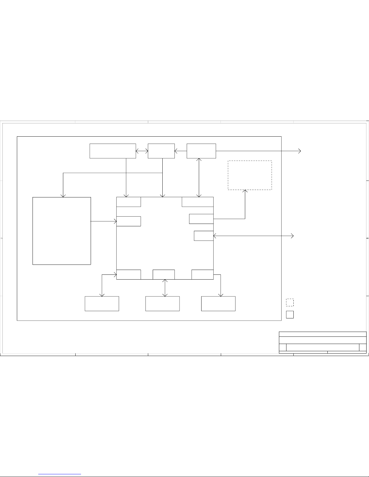
6 Evaluation of ECG and Respiration Specific Functions
The micro-controller receives the two-channel data from ADC through the SPI interface to send to the PC.
The software is designed to handle the following activities:
• Data acquisition
• ADC Lead off detection
• DC signal removal
• Multi band pass filtering
• ECG lead formation
• QRS (HR) detection
• RR Detection
• USB communication
• Firmware upgrade through USB
The high level architecture of the firmware implementation for the ADS1292R is given below:
30
ADS1x9xECG-FE Demonstration Kit SLAU384A–December 2011–Revised April 2012
Copyright © 2011–2012, Texas Instruments Incorporated
Submit Documentation Feedback
Page 31
1. Read ADS1x9x data
2. Process raw data
3. Compute HR and RR.
4. Stream data to PC
application through
USB.
5. Update status on
LED.
1. Update/read reg.
2. Interface with PC
app.
3. Update status
LED’s
Main loop : States
USB Receive
and Transmit
DMA Handler
ADS1292R REG
Configuration
ADS1292R Data
streaming
ADS1292R Data
dumping
ADS1292R Firmware
upgrade
1. Read packet from
memory.
2. Transfer data to PC
application through
USB.
3. Update Status on
LED’s.
1. Force firmware
to BSL code.
2. Upgrade
Firmware.
3. Reset firmware.
Initialize Peripherals
&
System parameters.
Start
ADS1292R
DRDY interrupt
.
1. Monitor user
commands.
ADS1292R IDLE
ADS1292R
SPI interrupt .
ADS1292R Data
Recording
1. Read ADS1292R data
2. Filter raw ECG data
3. Compute HR and RR.
4. Store packet to memory.
5. Update status on LED.
www.ti.com
Evaluation of ECG and Respiration Specific Functions
6.1 Evaluation Mode (Analysis Mode)
Figure 35. Firmware Architecture
The PC application consists of a LabVIEW front-end GUI with a back-end DLL written using C++. The DLL
interfaces with the Windows USB driver and communicates to the demonstration kit. The LabVIEW front
end GUI uses function calls to communicate with the demonstration kit through the DLL.
There are two general operating modes available in the system.
1. Evaluation Mode (Analysis Mode)
2. Live Data Streaming Mode
The Analysis Mode is used for the following requests:
1. Register setting
2. Register read
3. Data acquire
Firmware configures the ADC registers with default values during power on. Users can change the
register settings through the PC application GUI. The register setting request from the PC is processed by
the firmware and the appropriate register set command will be sent to the ADC.
During the data acquire request, the firmware will process the number of samples to be acquired as set in
the GUI. The firmware instructs the ADC to start the data conversion in continuous mode. Based on the
sampling rate configured, the ADC generates data ready pulses (DRDY) which are used by the microcontroller to indicate when to read data back. The data is stored in the onboard flash memory and later
sent to the PC application in individual packets. Each packet contains 8 samples which are 24bits in
length.
SLAU384A–December 2011–Revised April 2012 ADS1x9xECG-FE Demonstration Kit
Submit Documentation Feedback
Copyright © 2011–2012, Texas Instruments Incorporated
31
Page 32

Data Packetize Module
(CH1 and CH2)
Data Acquisition
ADC data DRDY
Interrupt
USB
PC Application
SPI Interrupt
2 Channel Data
Reader
ADS1292R Configuration
Module
ADS1292R DATA FLOW DIAGRAM:
ECG and Respiration Evaluation Mode
Decode PC
Commands
USB
SPI
Evaluation of ECG and Respiration Specific Functions
Figure 36. Evaluation Mode Data Flow for ADS1292R
www.ti.com
6.2 Live Data Streaming Mode
The Live ECG / Live Respiration data streaming can be started from the PC applicationLive ECG \ RESP
Display tab by clicking Start Data Streaming. The PC application will set the sampling rate to 500SPS
before requesting the firmware to start the live data streaming.
The firmware will instruct the converter to run in continuous conversion mode, monitoring the DRDY
interrupt for notification as to when new data is ready. Based on the interrupt, the firmware reads the data
from the ADC.
The firmware applies the following filters on the data read:
1. DC removal IIR filter
2. Multiband-pass FIR filter with 50/60 Hz notch (user selectable) or band-pass filter
The filtered signal is used for detecting the heart rate, respiration rate and deriving ECG leads. Filters are
applied only for live data streaming mode.
The system data flow diagram for live data stream mode is given in Figure 37.
32
ADS1x9xECG-FE Demonstration Kit SLAU384A–December 2011–Revised April 2012
Copyright © 2011–2012, Texas Instruments Incorporated
Submit Documentation Feedback
Page 33

FIR
Filters for
ECG (CH2)
& Respiration (CH1)
Data Acquisition
From ADC
ADC data DRDY
Interrupt
MemoryUSB
PC Application
SPI Interrupt
2 ChannelData
Reader
IIR
Filter
(DC Removal)
QRS
Algorithm
(HR) CH2
Lead Off
Status
Respiration
Rate
Algorithm
(RR) CH1
ECG signal
Respiration signal
ADS1292R DATA FLOW DIAGRAM:
PROCESSED ECG and RESPIRATION
DRDY
Interrupt
Decode PC
Commands
Lead Off Status
Lead Off Status
HR
1 ECG Lead
1 RESPIRATION CH.
Lead Off Status
RR
USB
SPI
-1
-1
Y(z) 1 - z
H(z) = =
X(z) 1 - az
www.ti.com
Evaluation of ECG and Respiration Specific Functions
Figure 37. Live Data Stream Mode Data Flow for ADS1292R
6.2.1 Filters
IIR Filter - DC signal removal
1st Order IIR filter is used to remove the DC component from the acquired data. The following transfer
function is used for the filter:
To provide DC attenuation at 22dB, the value of alpha is chosen as 0.992. The IIR filter output is scaled
down to 16-bit and then provided to the FIR filter. The frequency response for the IIR filter is shown in
Figure 38.
(1)
SLAU384A–December 2011–Revised April 2012 ADS1x9xECG-FE Demonstration Kit
Submit Documentation Feedback
Copyright © 2011–2012, Texas Instruments Incorporated
33
Page 34

Evaluation of ECG and Respiration Specific Functions
Figure 38. Frequency Response for the IIR Filter
www.ti.com
Multiband-pass Filter
Multiband-pass filter (MBF) is used for removing unwanted signals and power line noise from the live data.
The MBF digital filter is a 161 order FIR filter with Hamming window having cut-off at 150Hz and notch at
50/60 Hz. The notch frequency is selectable from the PC application. This filter provides a very sharp cutoff around 150 Hz with attenuation more than 30 dB at the stop band. The notch at 50/60 Hz provides
attenuation of more than 30 dB. Sampling frequency is 500 samples/ second.
The frequency response of the filter with a 50 Hz notch is shown in Figure 39, Figure 40, and Figure 41.
Figure 39. Frequency Response for the MBF Filter (Full View)
34
ADS1x9xECG-FE Demonstration Kit SLAU384A–December 2011–Revised April 2012
Copyright © 2011–2012, Texas Instruments Incorporated
Submit Documentation Feedback
Page 35

www.ti.com
Evaluation of ECG and Respiration Specific Functions
Figure 40. Frequency Response for the MBF Filter (50Hz Notch)
Figure 41. Frequency Response for the MBF Filter (Sharp cut off Around 150Hz)
Band Pass Filter
PC application allows the selection of a 161 order muscle artifact filter, which has a passband of 0.67 Hz
to 40 Hz. This filter provides a sharp cut-off at 40 Hz with attenuation of 30 dB at the stop band. The
frequency response for the filter is shown in Figure 42.
Figure 42. Frequency Response for the Band Pass Filter
SLAU384A–December 2011–Revised April 2012 ADS1x9xECG-FE Demonstration Kit
Submit Documentation Feedback
35
Copyright © 2011–2012, Texas Instruments Incorporated
Page 36

Evaluation of ECG and Respiration Specific Functions
6.2.2 Lead Derivation
The demonstration kit is configured to generate two ECG leads (Lead I and Lead II) from the four
electrodes using two channels of the ADS1192 and ADS1292 data. The other four ECG leads are
computed from Lead I and Lead II using the following equations:
Lead III = Lead II - Lead I
Lead aVR = - Lead II + 0.5 * Lead III
Lead aVL = Lead I - 0.5 * Lead II
Lead aVF = Lead III + 0.5 * Lead
The ADS1292R demonstration kit is configured to generate one ECG lead (Lead I) and one respiration
channel from the four electrodes using the two channels.
6.2.3 QRS and Respiration Rate Detection
QRS detection is based on first derivative of the Lead I ECG signal and threshold. Once five consecutive
QRS are detected, the heart rate is calculated by taking average of the five RR intervals.
The following steps are involved for calculating heart rate:
1. Calculate first derivative of the Lead I ECG signal samples. The first derivative for any sample is
calculated as
y0(n) = |x(n+1) – x(–1)|
Where,
y0(n) is the first derivative.
x (n+1) is the sample value for (n + 1) th sample.
x (n – 1) is the sample value for (n – 1) th sample.
2. The initial two seconds of the first derivative is stored in a buffer and the maximum value (P) in this
buffer is obtained.
3. Calculate the threshold as 0.7 x P.
4. Whenever a derivative crosses the threshold, the ECG sample index (S1) of that particular sample is
marked.
5. The QRS peak is detected by scanning the next 40 derivatives (MAXIMA_SEARCH_WINDOW = 40)
and obtaining the maxima (M1) .This maxima (M1) value is stored in another buffer.
www.ti.com
6. After detecting a QRS peak, the next 50 samples (SKIP_WINDOW = 50) are skipped to take care of
the minimum RR interval that can occur in the case of maximum detectable heart rate (i.e. 240 BPM).
7. Next five QRS peaks are detected by repeating steps 4 to 7.
8. RR interval is calculated as the number of samples between two consecutive QRS peaks.
9. Heart rate is calculated using the below formula HR per Minute = (60 * Sampling Rate)/ (Average RR
interval for 5 consecutive RR intervals )
10. Threshold also gets recalculated from the QRS peak values detected.
36
ADS1x9xECG-FE Demonstration Kit SLAU384A–December 2011–Revised April 2012
Copyright © 2011–2012, Texas Instruments Incorporated
Submit Documentation Feedback
Page 37

www.ti.com
Respiration rate for boards with the ADS1292R installed is calculated from the respiration waveform using
the similar algorithm mentioned above.
USB Receive and transmit module
The processed ECG and Respiration data including the heart rate, lead-off status, and respiration rate is
communicated to the PC, packet by packet, through the ECG interface. The packet contains 14 samples
of data, each being 16bits in width.
7 USB-Based Firmware Upgrade
The firmware on the ADS1x9xECG-FE can be changed from the PC application by selecting the
Firmware Upgrade option on the PC application. At the end of the firmware upgrade, the system issues a
reset command and will reload with new firmware. The firmware upgrade process steps are represented in
the below screen shots:
1. Select PC application menu File> Load Firmware
USB-Based Firmware Upgrade
Figure 43. PC Application Firmware Upgrade - 1
2. The firmware upgrade application window and the application will detect the connected ADS1x9xECG-
FE.
SLAU384A–December 2011–Revised April 2012 ADS1x9xECG-FE Demonstration Kit
Submit Documentation Feedback
37
Copyright © 2011–2012, Texas Instruments Incorporated
Page 38

Connector Interface
3. Browse and select the firmware binary file (.txt file) and click “Upgrade Firmware”
www.ti.com
Figure 44. PC Application Firmware Upgrade - 2
Figure 45. PC Application Firmware Upgrade - 3
NOTE: The default firmware will be available at C:\Program Files\Texas
Instruments\ADS1x9xevm\Firmware.
4. Device will reset and come up with new firmware with itself.
8 Connector Interface
The following connectors used for external interface to ADS1x9x ECG recorder board.
• DB9
• USB mini connector
38
ADS1x9xECG-FE Demonstration Kit SLAU384A–December 2011–Revised April 2012
Copyright © 2011–2012, Texas Instruments Incorporated
Submit Documentation Feedback
Page 39

www.ti.com Connector Interface
8.1 DB9 ECG Electrode Connector
Figure 46. DB9 ECG Connector Pin Outs
NO Signal Description
1 ERA
2 ELA
3 ELL
4 ERL
5 NC No Connect
6 NC No Connect
7 NC No Connect
8,9 ECG_SHD_DRV
8.2 USB Mini Connector
Figure 47. USB Mini Connector Pin Outs
NO Signal Description
1 VBUS USB power 5 V
2 D– USB DM
3 D+ USB DP
4 ID NC
5 GND GND
SLAU384A–December 2011–Revised April 2012 ADS1x9xECG-FE Demonstration Kit
Submit Documentation Feedback
39
Copyright © 2011–2012, Texas Instruments Incorporated
Page 40

Appendix A ECG Cable Details
The DB9 ECG connector uses the following pin out.
www.ti.com
Pin Electrode Name
1 RA
2 LA
3 LL
4 RL
5 Open
6 Open
7 Open
8 Shield
9 Shield
The ECG cable can be ordered through http://www.biometriccables.com/ using the part number
N26082011.
40
ECG Cable Details SLAU384A–December 2011–Revised April 2012
Figure 48. ECG Cable Drawing
Copyright © 2011–2012, Texas Instruments Incorporated
Submit Documentation Feedback
Page 41

www.ti.com
Appendix B ADS1x9x EVM Bill of Materials (BOM)
The following pages show the bill of materials table, landscaped for readability.
SLAU384A–December 2011–Revised April 2012 ADS1x9x EVM Bill of Materials (BOM)
Submit Documentation Feedback
41
Copyright © 2011–2012, Texas Instruments Incorporated
Page 42

Appendix B
www.ti.com
Table 1. Bill of Materials
Quantity
Item ADS1292R ADS1292 ADS1192 Ref Des Description Manufacturer Part Number
1 1 1 1 Printed Wiring Board TI 6525569
2 0 0 0 ANT1 Not Installed
C1 ,C2, C3, C4, C5, C11,
C12, C20, C26, C51, C54,
3 0 0 0 C55, C57, C61, C69, C71, Not Installed
C73, C74, C78, C79, C80,
C83, C89, C90, C91, C92
C6, C34, C35, C36, C38, C41,
4 10 10 10 CAP CER 10UF 6.3V X5R 20% 0603 AVX 06036D106MAT2A
C43, C65, C70, C85
5 4 4 4 C7, C8, C21, C25 CAP CER 10PF 50V NP0 RF 0402 AVX 04025U100CAT2A
C9, C13, C15, C19, C28, C31,
C33, C39, C44, C52, C63,
6 18 18 18 CAP CER 0.1UF 16V X7R 0402 TDK C1005X7R1C104K
C64,C67, C72, C76, C77,
C84, C87
7 2 2 2 C10 CAP CER 4700PF 10V 0402 LOW DIST TaiyoYuden LMK105SD472KV-F
0 1 1 CAP CER 4700PF 10V 0402 LOW DIST Taiyo Yuden LMK105SD472KV-F
8 C24
1 0 0 CAP CER 0.047UF 10V 10% X7R 0402 Murata GRM155R71A473KA01D
C14, C18, C22, C27, C40,
9 8 8 8 CAP CERM 1.0UF 10% 6.3V X5R 0402 AVX 04026D105KAT2A
C58, C86, C88
10 0 0 0 C16, C59, C62 Not Installed
11 2 2 2 C17, C66 CAP CER 0.22UF 16V X7R 0402 Murata GRM155R71C224KA12D
12 1 1 1 C23 CAP CER 1500PF 50V X7R 0402 AVX 04025C152JAT2A
13 2 2 2 C29, C30 CAP CER 12PF 5% 50V NP0 0402 AVX 04025A120JAT2A
14 1 1 1 C32 CAP CER 0.47UF 16V X5R 0402 TDK C1005X5R1C474K
15 3 3 3 C37, C81, C82 CAP CER 2.2UF 4.0V X5R 20% 0402 AVX 04024D225MAT2A
16 2 2 2 C42, C75 CAP CERM 10000PF 5% 16V X7R 0402 AVX 0402YC103JAT2A
17 2 0 0 C45, C47 CAP CERM 2200PF 10% 50V X7R 0402 AVX 04025C222KAT2A
18 2 0 0 CAP CER 0.1UF 16V X7R 0402 TDK C1005X7R1C104K
C46,C48
19 0 2 2 RES 0.0 OHM 1/10W 0402 SMD Panasonic ERJ-2GE0R00X
20 2 0 0 CAP CERM 2200PF 10% 50V X7R 0402 AVX 04025C222KAT2A
C49, C50
21 0 2 2 RES 0.0 OHM 1/10W 0402 SMD Panasonic ERJ-2GE0R00X
22 1 1 1 C53 CAP CER 4.7UF 6.3V X5R 0402 Murata GRM155R60J475ME87D
23 2 2 2 C56, C60 CAP CERM 47PF 5% 50V NP0 0402 AVX 04025A470JAT2A
24 1 1 1 C68 CAP TANT 22UF 6.3V 20% 0805 AVX TACH226M006XTA
25 1 1 1 D1 LED 470NM BLUE CLEAR 0603 SMD Rohm SMLE12BC7TT86
26 1 1 1 D2 LED 565NM GRN DIFF 0603 SMD Lumex SML-LX0603GW-TR
27 1 1 1 D3 DIODE SCHOTTKY 400MW 20V SOD123 Diodes Inc SD103CW-13-F
28 0 0 0 D4 Not Installed
29 0 0 0 L1, L2 NotInstalled
42
ADS1x9x EVM Bill of Materials (BOM) SLAU384A– December 2011–Revised April 2012
Submit Documentation Feedback
Copyright © 2011–2012, Texas Instruments Incorporated
Page 43

www.ti.com
Appendix B
Table 1. Bill of Materials (continued)
Quantity
Item ADS1292R ADS1292 ADS1192 Ref Des Description Manufacturer Part Number
30 1 1 1 L3 FERRITE CHIP 120 OHM 2000MA 0603 Murata BLM18PG121SN1D
31 2 2 2 L4,L7 FILTER CHIP 220 OHM 2A 0603 Murata BLM18EG221SN1D
32 1 1 1 L5 INDUCTOR POWER 3.3UH 1.3A SMD TDK VLF4012AT-3R3M1R3
33 0 0 0 L6 Not Installed
34 0 0 0 O1 Not Installed
35 1 1 1 O2 CRYSTAL 24.0000MHZ 10PF SMD Abracon ABM3B-24.000MHZ-10-1-U-T
36 1 1 1 O3 CRYSTAL 32.768KHZ 12.5PF SMD Abracon ABS07-32.768KHZ-T
37 1 1 1 P1 CONN RCPT MINIUSB B 5POS SMD R/A Molex Inc 513870530
38 0 0 0 P2 Not Installed
39 1 1 1 P3 3 pin Connector Samtec SSW-103-02-S-S-RA
40 0 0 0 P4 Not Installed
41 1 1 1 P5 CONN D-SUB RCPT R/A 9POS GOLD/FL TE Connectivity 1734354-1
42 0 0 0 P6 Not Installed
43 1 1 1 Q1 TRANSISTOR NPN 25V 50MA SOT-23 On Semi MMBT5089LT1G
R1, R3, R5, R6, R7, R8, R9,
R13, R15, R17, R21, R22,
R24, R25, R28, R39, R41,
R42, R47, R65, R67, R68,
44 0 0 0 Not Installed
R74, R76, R78, R79, R80,
R81, R83, R86, R88, R89,
R90, R91, R92, R93, R96,
R103
45 0 0 0 R2 Not Installed
R4, R46, R60, R97, R108,
46 7 7 7 RES 0.0 OHM .33W 0805 SMD Vishay/Dale CRCW08050000Z0EAHP
R111, R114
47 2 2 2 R10, R36 RES 1.0M OHM 1/10W 5% 0402 SMD Panasonic ERJ-2GEJ105X
48 3 3 3 R11, R12, R20 RES 33 OHM 1/10W 5% 0402 SMD Panasonic ERJ-2GEJ330X
49 1 1 1 R14 RES 1.40K OHM 1/10W 1% 0402 SMD Panasonic ERJ-2RKF1401X
1 0 0 R16
50 1 1 1 R73 RES 51K OHM 1/10W 5% 0402 SMD Panasonic ERJ-2GEJ513X
0 1 1 R85
R18, R19, R29, R30, R31,
51 15 15 15 R32, R33, R34, R38, R48, RES 10K OHM 1/10W 5% 0402 SMD Panasonic ERJ-2GEJ103X
R52, R53, R77, R94, R95
R23, R26, R27, R37, R40,
R44, R45, R49, R51, R54,
52 22 22 22 R55, R75, R84, R98, R99, RES 0.0 OHM 1/10W 0402 SMD Panasonic ERJ-2GE0R00X
R100, R102, R105, R106,
R109, R110, R113
53 2 2 2 R35, R117 RES 100K OHM 1/10W 5% 0402 SMD Panasonic ERJ-2GEJ104X
43
SLAU384A– December 2011–Revised April 2012 ADS1x9x EVM Bill of Materials (BOM)
Submit Documentation Feedback
Copyright © 2011–2012, Texas Instruments Incorporated
Page 44

Appendix B
www.ti.com
Table 1. Bill of Materials (continued)
Quantity
Item ADS1292R ADS1292 ADS1192 Ref Des Description Manufacturer Part Number
54 3 3 3 R43, R101,R107 RES 1.0K OHM 1/10W 5% 0402 SMD Panasonic ERJ-2GEJ102X
55 1 1 1 R50 RES 33K OHM 1/10W 5% 0402 SMD Panasonic ERJ-2GEJ333X
56 1 1 1 R56 RES 130 OHM 1/10W 5% 0402 SMD Panasonic ERJ-2GEJ131X
57 1 1 1 R57 RES 220 OHM 1/10W 5% 0402 SMD Panasonic ERJ-2GEJ221X
58 1 1 1 R58 RES 47K OHM 1/10W 5% 0402 SMD Panasonic ERJ-2GEJ473X
59 1 1 1 R59 RES 46.4K OHM 1/10W 1% 0402 SMD Panasonic ERJ-2RKF4642X
60 1 1 1 R61 RES 30.9K OHM 1/10W 1% 0402 SMD Panasonic ERJ-2RKF3092X
61 4 0 0 R62, R64, R66, R72 RES 10.0M OHM 1/16W 1% 0402 SMD Panasonic CRCW040210M0FKED
62 2 0 0 RES 0.0 OHM 1/10W 0402 SMD Panasonic ERJ-2GE0R00X
R63, R71
63 0 2 2 RES 51K OHM 1/10W 5% 0402 SMD Panasonic ERJ-2GEJ513X
64 2 0 0 R69, R70 RES 40K OHM 0.15W 0.1% 0603 Vishay/Thin Film PAT0603E4002BST1
65 2 2 2 R82, R115 RES 100 OHM 1/10W 5% 0402 SMD Panasonic ERJ-2GEJ101X
66 0 0 0 R87 Not Installed
67 1 1 1 R104 RES 4.7K OHM 1/10W 5% 0402 SMD Panasonic ERJ-2GEJ472X
68 1 1 1 R112 RES 10 OHM 1/10W 5% 0402 SMD Panasonic ERJ-2GEJ100X
69 2 2 2 R116, R118 RES 0.0 OHM 1/10W 0402 SMD Panasonic ERJ-2GE0R00X
70 2 2 2 SW1,SW4 SWITCH LT 6MM 160GF 5MM HEIGHT Panasonic EVQ-21505R
71 2 2 2 SW2,SW3 SWITCH TACT 2.36MM SILVR G-WING C&K Components KT11P2SM34LFS
72 0 0 0 TP1-TP60
73 0 0 0 U1 Not Installed
74 1 1 1 U2 4-Channel ESD-Protection Array Texas Instruments TPD4E004DRYR
75 0 0 0 U3 Not Installed
76 0 0 0 U4 Not Installed
2 channel Analog to Digital Converter (24 bit
77 1 0 0 Texas Instruments ADS1292RIPBS
with resp)
U5
78 0 1 0 2 channel Analog to Digital Converter (24 bit) Texas Instruments ADS1292IPBS
79 0 0 1 2 channel Analog to Digital Converter (16 bit) Texas Instruments ADS1192IPBS
80 1 1 1 U7 MSP Microcontroller Texas Instruments MSP430F5529IPNR
81 1 1 1 U8 Power-Path Management IC Texas Instruments BQ24032ARHLR
82 1 1 1 U9 2 bit Voltage Level Shfter Texas Instruments TXS0102DCTR
83 1 1 1 U10 3V Low-Dropout Regulator Texas Instruments TPS73201DBVT
84 0 0 0 U11 Not Installed
85 0 0 0 U12 Not Installed
86 0 0 0 U13 Not Installed
87 1 1 1 U14 8Gb NAND Flash Micron MT29F8G08ABABAWP:B
88 0 0 0 U15 Not Installed
44
ADS1x9x EVM Bill of Materials (BOM) SLAU384A– December 2011–Revised April 2012
Submit Documentation Feedback
Copyright © 2011–2012, Texas Instruments Incorporated
Page 45

www.ti.com
Appendix B
Table 1. Bill of Materials (continued)
Quantity
Item ADS1292R ADS1292 ADS1192 Ref Des Description Manufacturer Part Number
89 1 1 1 U16 3.3V Linear Regulator Texas Instruments TPS73033DBVR
90 0 0 0 U17 Not Installed
91 1 1 1 U18 3.3V supervisors Texas Instruments TPS3825-33DBVT
Battery Assembly
92 0 0 0 Connector on battery CONN HOUSING 2POS .100 W/O RAMP Molex 22012021
93 0 0 0 Connector on battery CONN TERM CRIMP 18-24AWG TIN Molex 8030303
94 0 0 0 Battery 4.2VLi Ion Battery Power Stream GM065080
95 0 0 0 Battery Cable 22 AWG red color cable
96 0 0 0 Battery Cable 22 AWG black color cable
45
SLAU384A– December 2011–Revised April 2012 ADS1x9x EVM Bill of Materials (BOM)
Submit Documentation Feedback
Copyright © 2011–2012, Texas Instruments Incorporated
Page 46

Appendix C PCB Layout and Schematics
C.1 PCB Layout
The following pages show the PCB layout, landscaped for readability.
www.ti.com
46
PCB Layout and Schematics SLAU384A–December 2011–Revised April 2012
Copyright © 2011–2012, Texas Instruments Incorporated
Submit Documentation Feedback
Page 47

www.ti.com
PCB Layout
Figure 49. Top Layer Placement
47
SLAU384A– December 2011–Revised April 2012 PCB Layout and Schematics
Submit Documentation Feedback
Copyright © 2011–2012, Texas Instruments Incorporated
Page 48

PCB Layout
www.ti.com
Figure 50. Bottom Layer Placement
48
PCB Layout and Schematics SLAU384A–December 2011–Revised April 2012
Submit Documentation Feedback
Copyright © 2011–2012, Texas Instruments Incorporated
Page 49

www.ti.com
C.2 Schematics
The schematics are appended to the end of this data sheet.
Schematics
SLAU384A–December 2011–Revised April 2012 PCB Layout and Schematics
Submit Documentation Feedback
49
Copyright © 2011–2012, Texas Instruments Incorporated
Page 50
A
B
C
D
5 4 3 2 1
D
C
B
A
12345
Title
Size Document Number Rev
Date: Sheet of 7
ADS1x9xECG FE A
Block Diagram
1
B
Thursday, August 04, 2011
Battery
Power
Module
USB
I2C
SPI
USB
UART
JTAG
BT
Module
GPIO
SPI
GPIO
Flash
Memory
Micro SD
LEDs &
Keys
Optional
Must have modules
Data
Power
To PC
Application
1.ADS1292R - 24 bit 2 Ch
-- 1 Ch ECG
2.ADS1292 - 24 bit 2 Ch
-- 2 Ch ECG
3.ADS1192 - 16 bit 2 Ch
-- 2 Ch ECG
-- 1 Ch Respiration
Page 51

Place the decoupling capacitors close to power pins in layout
DNI
A
B
C
D
5 4 3 2 1
D
C
B
A
12345
Title
Size Document Number Rev
Date: Sheet of 7
ADS1x9xECG FE
ADS1292
A
2
B
Thursday, August 04, 2011
Note:
For two channel ECG Do the following modification
1) Mount 51K resistor in place of R71 and R63
2) Mount 0 Ohm resistors in place of C48, C46, C49 and C50
3) Make following components DNI
R66, R64, R72, R62, C47,C45,R70 and R69
External Clock
ELL
ELA
ERA
ERL
ECG_SHD_DRV
C45
2.2nF
R32 10K
R44
0E
R63
0E
1
ENB
2
GND
3
OUT
4
VDD
O1
NI
1
TP53
C69
NI
5
9
4
8
3
7
2
6
1
10
11
P5
482016042
R55
0E
R85
51K
R21
NI
R77
10K
C58
1uF
C24
4.7nF
1
TP38
L3
BLM18PG121SN1P
R62
10M (1%)
R4
0E
C15
0.1uF
1
TP11
R64
10M (1%)
C22
1uF
1
TP47
R26
0E
R6940K
C10
4.7nF
C19
0.1uF
R27
0E
R76
NI
DNI
C56
47pF
1
TP46
1
TP56
1
TP24
C14
1uF
1
TP52
1
TP42
R45
0E
R41
NI
C4
NI
C18
1uF
R36
1M
R34 10K
R37
0E
R54
0E
R66
10M (1%)
C60
47pF
C6
10uF
C49
2.2nF
R2
NI
1
TP16
R73
51K
R72
10M (1%)
C71
NI
R23
0E
1
PGA1N
2
PGA1P
3
IN1N
4
IN1P
5
IN2N
6
IN2P
7
PGA2N
8
PGA2P
9
VREFP10VREFN
11
VCAP1
12
AVDD13AVSS14CLKSEL
15
PWDN#/RESET#
16
START
17
CLK
18
CS#
19
DIN
20
SCLK
21
DOUT
22
DRDY#
23
DVDD
24
DGND
25
GPIO2/RCLK226GPIO1/RCLK1
27
VCAP2
28
RLDINV
29
RLDIN/RLDREF
30
RLDOUT
31
RESP_MODP/IN3P
32
RESP_MODN/IN3N
U5
ADS1292R
R70
40K
C50
2.2nF
C9
0.1uF
R71
0E
C23
1.5nF
1
TP15
+
-
3
4
1
52
U15
NI
1
TP34
C47
2.2nF
C87
0.1uF
C88
1uF
R16 NI
DNI
C48
0.1uF
C46
0.1uF
R116
0E
R118
0E
C89
NI
DNI
C90
NI
DNI
C92
NI
DNI
C91 NI
DNI
R35
100K
R117
100K
ADS_DVDD
ADS_DVDD
ADS_DVDD
VCC_3_3
ADS_DVDD
AVSS
ADS_AVDD
AVSS
AVSS
ADS_AVDD
AVSS
ADS_AVDD
AVSS
ADS_DVDD
ADC_GPIO2
ADC_GPIO1
ADC_CLK
ADC_CS
ADC_START
ADC_SCLK
ADC_RESET
ADC_DRDY
RESP_MOD_M
ERL
RESP_MOD_P
ADC_CLK_SCL
ADS_AVDD
AVSS
ADC_DOUT
ADC_DIN
AVSS
AVSS
ELL
Page 52

A
B
C
D
5 4 3 2 1
D
C
B
A
12345
Title
Size Document Number Rev
Date: Sheet of 7
ADS1x9xECG FE
A
ADS1292 Power Supply
3
B
Thursday, August 04, 2011
C38
10uF
C36
10uF
R60
0E
R61
30.9K
C39
0.1uF
1
IN
2
GND
3
EN
4
NR/FB
5
OUT
U10
TPS73201
R59
46.4K
1
TP32
C42
0.01uF
L5
3.3uH
R46
0E
C37
2.2uF
C40
1uF
C41
10uF
ADS_AVDD
VCC_BAT
AVSS
AVSS
Page 53

1% tol
5% tol
5% tol
A
B
C
D
5 4 3 2 1
D
C
B
A
12345
Title
Size Document Number Rev
Date: Sheet of 7
ADS1x9xECG FE A
USB, Micro SD, USB Interfaces
4
B
Thursday, August 04, 2011
SDCARD
DNI
1
TP10
C43
10uF
C63
0.1uF
1
RSV1
2
CS
3
DI
4
VCC
5
CLK
6
VSS
7
DO
8
RSV2
P2
NI
R75
0E
1
TP36
1
TP59
SW1
EVQ-21505R
1
IO12IO23IO34IO4
5
IO56IO67IO78IO8
9
GND
U11
NI
1
TP37
C64
0.1uF
R82
100E
1
NC1
2
NC2
3
NC3
4
NC4
5
NC5
6
R/B2#
7
R/B#
8
RE#
9
CE#
10
CE2#
11
NC6
12
VCC
13
VSS
14
NC7
15
NC8
16
CLE
17
ALE
18
WE#
19
WP#
20
DNU1
21
DNU2
22
DNU3
23
NC9
24
NC10
25
NC11
26
NC12
27
NC13
28
NC14
29
I/O0
30
I/O1
31
I/O2
32
I/O3
33
NC15
34
NC16
35
NC17
36
VSS
37
VCC
38
PRE/VSS2
39
NC18
40
NC19
41
I/O4
42
I/O5
43
I/O6
44
I/O7
45
NC20
46
NC21
47
NC22
48
NC23
U14
MT298G08AAAWP
R93 NI
DNI
R107
1K
1
TP41
1
TP58
1
IO12IO2
3
GND
4
IO35IO4
6
VCC
U2
TPD4E004DRYR
C7
10pF
R68
NI
D3 SD103AW-13-F
R67
NI
R102
0E
1
TP55
R109 0E
R98 0E
R106
0E
R14
1.4K
R12
33E
R101
1K
C52
0.1uF
1
TP30
1
TP33
C62
NI
R65
NI
C8
10pF
1
TP57
R10
1M
1
VBUS
2
D-
3
D+
4
ID
5
GND
6
SHIELD1
7
SHIELD2
8
8
9
9
10
10
11
11
P1
0513870530
C78
NI
1
TP54
R11 33E
R100
0E
R99
0E
R105
0E
R94
10K
R110
0E
+
C53
4.7uF
VCC_3_3
VCC_3_3
VCC_3_3
FLASH_CE
FLASH_CE2
FLASH_CLE
FLASH_ALE
FLASH_WE
FLASH_RE
FLASH_RB
FLASH_RB2
FLASH_IO0
FLASH_IO1
FLASH_IO2
FLASH_IO3
FLASH_IO4
FLASH_IO5
FLASH_IO6
FLASH_IO7
USD_CS
SPI_SIMO
SPI_SCLK
SPI_SOMI
VBUS
USB_DM
USB_DP
PUR
VUSB
Page 54

A
B
C
D
5 4 3 2 1
D
C
B
A
12345
Title
Size Document Number Rev
Date: Sheet of 75
ADS1x9xECG FE A
MSP430
B
Thursday, August 04, 2011
VCC
GND
1
TP28
C66
220nF
1
TP29
1
TP50
R24 NI
DNI
R95
10K
R58
47K
C86
1uF
C13
0.1uF
D1
SMLE12BC7TT86
C34
10uF
1
TP45
1
1
2
2
3
3
4
4
O2
ABM3B-24.000MHZ
1
TP26
C32
470nF
R113 0E
R83 NI
R56 130E
C65
10uF
C35
10uF
L4
BLM21PG220SN1B
R57 220E
C25
10pF
Q1
MMBT5089LT1G
1
TP9
1
TP18
O3
ABS07-32.768KHZ-T
C30
12pF
R20 33E
1
TP21
D2
SMLE12EC6TT86
C21
10pF
1
P6_4/CB4/A4
2
P6_5/CB5/A5
3
P6_6/CB6/A6
4
P6_7/CB7/A7
5
P7_0/CB8/A12
6
P7_1/CB9/A13
7
P7_2/CB10/A14
8
P7_3/CB11/A15
9
P5_0/A8/VREF+/VEREF+
10
P5_1/A9/VREFN/VEREFN
11
AVCC1
12
P5_4/XIN
13
P5_5/XOUT
14
AVSS1
15
P8_0
16
P8_1
17
P8_2
18
DVCC1
19
DVSS1
20
VCORE
41
P3_4/UCA0RXD/UCA0SOMI
42
P3_5/TB0_5
43
P3_6/TB0_6
44
P3_7/TB0OUTH/SVMOUT
45
P4_0/PM_UCB1STE/PM_UCA1CLK
46
P4_1/PM_UCB1SIMO/PM_UCB1SDA
47
P4_2/PM_UCB1SOMI/PM_UCB1SCL
48
P4_3/PM_UCB1CLK/PM_UCA1STE
49
DVSS2
50
DVCC2
51
P4_4/PM_UCA1TXD/PM_UCA1SIMO
52
P4_5/PM_UCA1RXD/PM_UCA1SOMI
53
P4_6/PM_NONE
54
P4_7/PM_NONE
55
P5_6/TB0_0
56
P5_7/TB0_1
57
P7_4/TB0_2
58
P7_5/TB0_3
59
P7_6/TB0_4
60
P7_7/TB0CLK/MCLK
61
VSSU
62
PU_0/DP
63
PUR
64
PU_1/DM
65
VBUS66VUSB
67
V18
68
AVSS2
69
P5_2/XT2IN
70
P5_3/XT2OUT
71
TEST/SBWTCK
72
PJ_0/TDO
73
PJ_1/TDI/TCLK
74
PJ_2/TMS
75
PJ_3/TCK
76
RST/NMI/SBWTDIO
77
P6_0/CB0/A078P6_1/CB1/A179P6_2/CB2/A280P6_3/CB3/A3
21
P1_0/TA0CLK/ACLK22P1_1/TA0_023P1_2/TA0_124P1_3/TA0_225P1_4/TA0_326P1_5/TA0_427P1_6/TA1CLK/CBOUT28P1_7/TA1_031P2_2/TA2CLK/SMCLK30P2_1/TA1_229P2_0/TA1_132P2_3/TA2_033P2_4/TA2_134P2_5/TA2_235P2_6/RTCCLK/DMAE036P2_7/UCB0STE/UCA0CLK37P3_0/UCB0SIMO/UCB0SDA38P3_1/UCB0SOMI/UCB0SCL39P3_2/UCB0CLK/UCA0STE40P3_3/UCA0TXD/UCA0SIMO
U7
MSP430F5529IPNR
L7
BLM21PG220SN1B
SW4
EVQ-21505R
1
TP40
1
B2
2
GND
3
VCCA
4
A2
5
A1
6
OE
7
VCCB
8
B1
U9
TXS0102DCTR
C29
12pF
C83 NI
DNI
C85
10uF
C84
0.1uF
1
TP43
R84
0E
1
TP39
1
TP23
R18
10K
C31
0.1uF
C67
0.1uF
1
TP27
1
42
3
SW2
KT11P2SM34LFS
R19
10K
R49
0E
C76
0.1uF
C17
220nF
C33
0.1uF
1
NC
2
GND
3
I/O
4
CLK
5
VCC
6
NC
P4
851-93-006-20-001000
R40
0E
MSP_DVDD
MSP_DVDD
MSP_DVDD
MSP_AVDD
MSP_AVDD
MSP_DVDD
VCC_3_3
VCC_3_3
MSP_DVDD
VCC_3_3
FLASH_IO4
FLASH_IO5
FLASH_IO6
FLASH_IO7
FLASH_IO0
FLASH_IO1
FLASH_IO2
FLASH_IO3
FLASH_CE
FLASH_CLE
FLASH_ALE
FLASH_WE
FLASH_RE
PUR
VBUS
USB_DM
USB_DP
SPI_SCLK
ADC_SCLK
ADC_RESET
ADC_START
ADC_DRDY
FLASH_RB
ADC_GPIO2
ADC_GPIO1
ADC_CLK_SCL
ADC_CLK
BAT_SCL
BAT_SDA
STAT2
STAT1
BT_RX
BT_TX
BT_SLOW_CLK
BT_NSHUTDOWN
FLASH_RB2
FLASH_CE2
ADC_CS
POW_CE
SYS_RESET
VUSB
SPI_SIMO
SPI_SOMI
BT_CTS
USD_CS
BT_CS1
BT_RTS
SBWTDIO
SBWTCLK
TCK
KEY2
KEY1
TMS
XT2IN TDI
XT2OUT
TDO
LED2
XOUT
LED1
XIN
SBWTCLK
TCK
KEY2
KEY1
TMS
XT2IN
TDI
XT2OUT
TDO
LED2
LED1
SBWTDIO
ADC_DOUT
ADC_DIN
Page 55

3.3V Voltage Supervisor
3.3V Power Supply
Battery Fuel Gauge
Battery Management
DNI
A
B
C
D
5 4 3 2 1
D
C
B
A
12345
Title
Size Document Number Rev
Date: Sheet of 7
ADS1x9xECG FE A
Power Supply
6
B
Thursday, August 04, 2011
DNI
C74
NI
C70
10uF
R52
10K
1
TP22
1
TP48
1
TP20
R31 10K
1
TP60
R89
NI
R112
10E
R91 NI
C68
22uF
1
TP49
R114 0E
1
1
2
2
3
3
P3
SSW-103-02-S-S-RA
R39 NI
DNI
C77
0.1uF
R53 10K
D4
NI
1
BAT_P
2
BAT_M
P6
NI
1
TP51
C79
NI
C81
2.2uF
5
VDD
4
MR#
3
RESET
2
GND
1
RESET#
U18
TPS3825
C80
NI
C82
2.2uF
R51 0E
C28
0.1uF
R50
33K
R29 10K
R47
NI
R33
10K
R92 NI
C26
NI
R38 10K
1
LDO
2
STAT1
3
STAT2
4
AC
5
BAT1
6
BAT2
7
ISET2
8
PSEL
9
CE
10
ISET1
11
VSS
15
OUT3
16
OUT2
17
OUT1
18
ACPG#
19
USBPG#_/_VBSEL
12
TS
13
DPPM
14
TMR
20
USB
21
TP
U8
BQ24032ARHLR
R48
10K
R103
NI
R28 NI
DNI
R115
100E
1
TP25
C75
0.01uF
1
TP17
R42 NI
DNI
R87
NI
C20
NI
R104
4.7K
1
RBI
2
VCC
3
VSS
4
SCL
5
SDA
6
BAT
7
SRN
8
SRP
9
GPIO
10
PGM
11
VSS1
U17
NI
C73
NI
C44
0.1uF
R88
NI
C72
0.1uF
R111
0E
R43
1K
1
IN
2
GND
3
EN4NR
5
OUT
U16
TPS73033
R96 NI
R90
NI
R97
0E
1
42
3
SW3
KT11P2SM34LFS
C16
NI
R108
0E
1
TP13
1
TP31
R30 10K
C27
1uF
VCC_3_3
VCC_3_3
VCC_3_3
AVSS
VCC_BAT
VCC_BAT
ADS_AVDD
VBUS
STAT2
STAT1
BAT_SDA
BAT_SCL
SYS_RESET
POW_CE
PSEL
ISET2
ISET1
ACPG
POW_CE
TS
STAT2
PACK_PPACK_P
STAT1
USBPG
PSEL
ISET2
ISET1ACPG
POW_CE
TS
STAT2
PACK_P
STAT1
USBPG
Page 56

R86 R13
Mount
Mount
Do Not When PANI315 Bluetooth module is used
When A1101R09A Bluetooth module is used
Mount
Do Not
Mount
Description
(Default)
A
B
C
D
5 4 3 2 1
D
C
B
A
12345
Title
Size Document Number Rev
Date: Sheet of 7
Bluetooth Module
AADS1x9xECG FE
7
B
Thursday, August 04, 2011
DNI
C1
NI
1
TP6
R22
NI
C59
NI
C2
NI
C57
NI
1
TP4
C12
NI
1
TP1
1
GND
13
RF
9
IO2
24
IO1
8
SLOW_CLK_IN
6
HCI_TX
5
HCI_RX
4
HCI_RTS
3
HCI_CTS
7
AUD_FSYNC
19
AUD_CLK
18
AUD_IN
17
AUD_OUT
2
TX_DBG
12
GND
10
MLDO_OUT
15
MLDO_IN
11
CL1_5_LDO_IN
22
VDD_IO
16
NSHUTD
23
I2C_SCL
21
I2C_SDA
14
GND20GND
U1
NI
R81
NI
1.8V
6
IN
4
EN
1
OUT
2
NC1
3
GND5NC2
U13
NI
R9
NI
L6
NI
R5
NI
R13 NI
DNI
R3 NI
R86 NI
R78
NI
1
TP44
1
DIR1
2
DIR2
3
A1
4
A2
5
A3
6
A4
9
OE#
16
VCCA
7
DIR3
8
DIR4
11
B4
12
B3
13
B2
14
B1
15
VCCB
10
GND
U4
NI
R8
NI
1
TP2
R74
NI
1
TP8
C61
NI
C5
NI
C55
NI
C54
NI
C51
NI
R17
NI
ANT1
NI
C11
NI
1
TP7
1
DNC1
2
DNC2
3
DNC3
4
NC1
5
NC2
6
NC3
9
SCLK
16
NC
18
VDD
19
NC4
20
NC6
21
NC5
22
DNC6
23
DNC5
24
DNC4
7
VDCOUP1
10
MISO/GDO1
11
MOSI
12
CS#
13
GDO0
14
GDO2
15
VDCOUP2
8
GND17GND
U12
NI
R6 NI
1
TP3
R15
NI
R80 NI
C3
NI
5
DIR
3
A2
2
A1
1
VCCA8VCCB
7
B1
6
B2
4
GND
U3
NI
L2
NI
1
TP35
L1
NI
R79
NI
R7
NI
R25
NI
1
TP5
R1
NI
VCC_3_3
VCC_1_8
VCC_1_8VCC_3_3
VCC_1_8 VCC_3_3
VCC_1_8
VCC_3_3
VCC_3_3
BT_TX
BT_RTS
BT_RX
BT_NSHUTDOWN
BT_SLOW_CLK
SPI_SIMO
SPI_SOMI
BT_CS1
SPI_SCLK
BT_CTS
PAN_RX
PAN_TX
SLOW_CLK
PAN_CTS
SHUTDOWN
PAN_RTS
GDO2
PAN_RX
BT_IN_CTS
PAN_TX
SLOW_CLK
PAN_CTS
SHUTDOWN
PAN_RTS
GDO2
BT_IN_CTS
Page 57

Evaluation Board/Kit Important Notice
Texas Instruments (TI) provides the enclosed product(s) under the following conditions:
This evaluation board/kit is intended for use for ENGINEERING DEVELOPMENT, DEMONSTRATION, OR EVALUATION PURPOSES
ONLY and is not considered by TI to be a finished end-product fit for general consumer use. Persons handling the product(s) must have
electronics training and observe good engineering practice standards. As such, the goods being provided are not intended to be complete
in terms of required design-, marketing-, and/or manufacturing-related protective considerations, including product safety and environmental
measures typically found in end products that incorporate such semiconductor components or circuit boards. This evaluation board/kit does
not fall within the scope of the European Union directives regarding electromagnetic compatibility, restricted substances (RoHS), recycling
(WEEE), FCC, CE or UL, and therefore may not meet the technical requirements of these directives or other related directives.
Should this evaluation board/kit not meet the specifications indicated in the User’s Guide, the board/kit may be returned within 30 days from
the date of delivery for a full refund. THE FOREGOING WARRANTY IS THE EXCLUSIVE WARRANTY MADE BY SELLER TO BUYER
AND IS IN LIEU OF ALL OTHER WARRANTIES, EXPRESSED, IMPLIED, OR STATUTORY, INCLUDING ANY WARRANTY OF
MERCHANTABILITY OR FITNESS FOR ANY PARTICULAR PURPOSE.
The user assumes all responsibility and liability for proper and safe handling of the goods. Further, the user indemnifies TI from all claims
arising from the handling or use of the goods. Due to the open construction of the product, it is the user’s responsibility to take any and all
appropriate precautions with regard to electrostatic discharge.
EXCEPT TO THE EXTENT OF THE INDEMNITY SET FORTH ABOVE, NEITHER PARTY SHALL BE LIABLE TO THE OTHER FOR ANY
INDIRECT, SPECIAL, INCIDENTAL, OR CONSEQUENTIAL DAMAGES.
TI currently deals with a variety of customers for products, and therefore our arrangement with the user is not exclusive.
TI assumes no liability for applications assistance, customer product design, software performance, or infringement of patents or
services described herein.
Please read the User’s Guide and, specifically, the Warnings and Restrictions notice in the User’s Guide prior to handling the product. This
notice contains important safety information about temperatures and voltages. For additional information on TI’s environmental and/or
safety programs, please contact the TI application engineer or visit www.ti.com/esh.
No license is granted under any patent right or other intellectual property right of TI covering or relating to any machine, process, or
combination in which such TI products or services might be or are used.
FCC Warning
This evaluation board/kit is intended for use for ENGINEERING DEVELOPMENT, DEMONSTRATION, OR EVALUATION PURPOSES
ONLY and is not considered by TI to be a finished end-product fit for general consumer use. It generates, uses, and can radiate radio
frequency energy and has not been tested for compliance with the limits of computing devices pursuant to part 15 of FCC rules, which are
designed to provide reasonable protection against radio frequency interference. Operation of this equipment in other environments may
cause interference with radio communications, in which case the user at his own expense will be required to take whatever measures may
be required to correct this interference.
EVM Warnings and Restrictions
It is important to operate this EVM within the input voltage range of 0 V to 5 V and the output voltage range of 0 V to 5 V .
Exceeding the specified input range may cause unexpected operation and/or irreversible damage to the EVM. If there are questions
concerning the input range, please contact a TI field representative prior to connecting the input power.
Applying loads outside of the specified output range may result in unintended operation and/or possible permanent damage to the EVM.
Please consult the EVM User's Guide prior to connecting any load to the EVM output. If there is uncertainty as to the load specification,
please contact a TI field representative.
During normal operation, some circuit components may have case temperatures greater than 30° C. The EVM is designed to operate
properly with certain components above 30° C as long as the input and output ranges are maintained. These components include but are
not limited to linear regulators, switching transistors, pass transistors, and current sense resistors. These types of devices can be identified
using the EVM schematic located in the EVM User's Guide. When placing measurement probes near these devices during operation,
please be aware that these devices may be very warm to the touch.
Mailing Address: Texas Instruments, Post Office Box 655303, Dallas, Texas 75265
Copyright © 2012, Texas Instruments Incorporated
Page 58

IMPORTANT NOTICE
Texas Instruments Incorporated and its subsidiaries (TI) reserve the right to make corrections, modifications, enhancements, improvements,
and other changes to its products and services at any time and to discontinue any product or service without notice. Customers should
obtain the latest relevant information before placing orders and should verify that such information is current and complete. All products are
sold subject to TI’s terms and conditions of sale supplied at the time of order acknowledgment.
TI warrants performance of its hardware products to the specifications applicable at the time of sale in accordance with TI’s standard
warranty. Testing and other quality control techniques are used to the extent TI deems necessary to support this warranty. Except where
mandated by government requirements, testing of all parameters of each product is not necessarily performed.
TI assumes no liability for applications assistance or customer product design. Customers are responsible for their products and
applications using TI components. To minimize the risks associated with customer products and applications, customers should provide
adequate design and operating safeguards.
TI does not warrant or represent that any license, either express or implied, is granted under any TI patent right, copyright, mask work right,
or other TI intellectual property right relating to any combination, machine, or process in which TI products or services are used. Information
published by TI regarding third-party products or services does not constitute a license from TI to use such products or services or a
warranty or endorsement thereof. Use of such information may require a license from a third party under the patents or other intellectual
property of the third party, or a license from TI under the patents or other intellectual property of TI.
Reproduction of TI information in TI data books or data sheets is permissible only if reproduction is without alteration and is accompanied
by all associated warranties, conditions, limitations, and notices. Reproduction of this information with alteration is an unfair and deceptive
business practice. TI is not responsible or liable for such altered documentation. Information of third parties may be subject to additional
restrictions.
Resale of TI products or services with statements different from or beyond the parameters stated by TI for that product or service voids all
express and any implied warranties for the associated TI product or service and is an unfair and deceptive business practice. TI is not
responsible or liable for any such statements.
TI products are not authorized for use in safety-critical applications (such as life support) where a failure of the TI product would reasonably
be expected to cause severe personal injury or death, unless officers of the parties have executed an agreement specifically governing
such use. Buyers represent that they have all necessary expertise in the safety and regulatory ramifications of their applications, and
acknowledge and agree that they are solely responsible for all legal, regulatory and safety-related requirements concerning their products
and any use of TI products in such safety-critical applications, notwithstanding any applications-related information or support that may be
provided by TI. Further, Buyers must fully indemnify TI and its representatives against any damages arising out of the use of TI products in
such safety-critical applications.
TI products are neither designed nor intended for use in military/aerospace applications or environments unless the TI products are
specifically designated by TI as military-grade or "enhanced plastic." Only products designated by TI as military-grade meet military
specifications. Buyers acknowledge and agree that any such use of TI products which TI has not designated as military-grade is solely at
the Buyer's risk, and that they are solely responsible for compliance with all legal and regulatory requirements in connection with such use.
TI products are neither designed nor intended for use in automotive applications or environments unless the specific TI products are
designated by TI as compliant with ISO/TS 16949 requirements. Buyers acknowledge and agree that, if they use any non-designated
products in automotive applications, TI will not be responsible for any failure to meet such requirements.
Following are URLs where you can obtain information on other Texas Instruments products and application solutions:
Products Applications
Audio www.ti.com/audio Automotive and Transportation www.ti.com/automotive
Amplifiers amplifier.ti.com Communications and Telecom www.ti.com/communications
Data Converters dataconverter.ti.com Computers and Peripherals www.ti.com/computers
DLP® Products www.dlp.com Consumer Electronics www.ti.com/consumer-apps
DSP dsp.ti.com Energy and Lighting www.ti.com/energy
Clocks and Timers www.ti.com/clocks Industrial www.ti.com/industrial
Interface interface.ti.com Medical www.ti.com/medical
Logic logic.ti.com Security www.ti.com/security
Power Mgmt power.ti.com Space, Avionics and Defense www.ti.com/space-avionics-defense
Microcontrollers microcontroller.ti.com Video and Imaging www.ti.com/video
RFID www.ti-rfid.com
OMAP Mobile Processors www.ti.com/omap
Wireless Connectivity www.ti.com/wirelessconnectivity
TI E2E Community Home Page e2e.ti.com
Mailing Address: Texas Instruments, Post Office Box 655303, Dallas, Texas 75265
Copyright © 2012, Texas Instruments Incorporated
Page 59

Authorized Distribution Brand:
Website:
Welcome to visit www.ameya360.com
Contact Us:
Address:
401 Building No.5, JiuGe Business Center, Lane 2301, Yishan Rd
Minhang District, Shanghai , China
Sales:
Direct +86 (21) 6401-6692
Email amall@ameya360.com
QQ 800077892
Skype ameyasales1 ameyasales2
Customer Service:
Email service@ameya360.com
Partnership:
Tel +86 (21) 64016692-8333
Email mkt@ameya360.com
 Loading...